Carbon Nanomaterials for Next Generation Interconnects and ...
Carbon Nanomaterials for Next Generation Interconnects and ...
Carbon Nanomaterials for Next Generation Interconnects and ...

You also want an ePaper? Increase the reach of your titles
YUMPU automatically turns print PDFs into web optimized ePapers that Google loves.
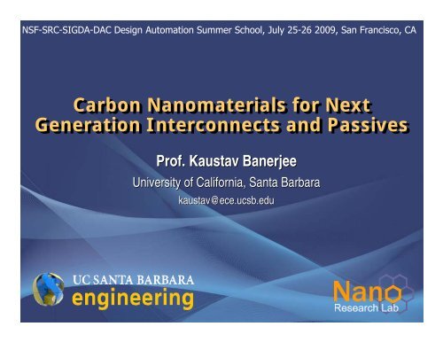
NSF-SRC-SIGDA-DAC Design Automation Summer School, July 25-26 2009, San Francisco, CA<br />
<strong>Carbon</strong> <strong>Nanomaterials</strong> <strong>for</strong> <strong>Next</strong><br />
<strong>Generation</strong> <strong>Interconnects</strong> <strong>and</strong> Passives<br />
Prof. Kaustav Banerjee<br />
University of Cali<strong>for</strong>nia, Santa Barbara<br />
kaustav@ece.ucsb.edu<br />
Kaustav Banerjee, UCSB KEYNOTE: 12 th IEEE Workshop on Signal Propagation on <strong>Interconnects</strong> (SPI), Avignon, France, May 15 th , 2008
Outline<br />
Part I:<br />
• Limitations of Copper <strong>Interconnects</strong><br />
• <strong>Carbon</strong> <strong>Nanomaterials</strong>: : Basics<br />
• Circuit Elements of CNT/GNR<br />
• Fabrication <strong>and</strong> Integration of CNT/GNR<br />
<strong>Interconnects</strong><br />
Part II:<br />
• Per<strong>for</strong>mance Evaluation of CNT/GNR <strong>Interconnects</strong><br />
• Electro-thermal thermal Analysis of CNT Vias<br />
• High-Frequency Analysis of CNT <strong>Interconnects</strong><br />
• Passives <strong>and</strong> Other Applications<br />
Kaustav Banerjee, Kaustav UC Santa Banerjee Barbara<br />
Design Design Automation Automation Summer Summer School, July School 25-26 Lecture, 2009, San July Francisco, 26 2009, CA San Francisco, CA
Part I<br />
Kaustav Banerjee, Kaustav UC Santa Banerjee Barbara<br />
Design Design Automation Automation Summer Summer School, July School 25-26 Lecture, 2009, San July Francisco, 26 2009, CA San Francisco, CA
<strong>Interconnects</strong> in ICs….<br />
By volume, ICs have<br />
become “all wires”…<br />
SEM image of IBM’s six-level<br />
Cu interconnect technology<br />
<strong>Interconnects</strong> have become the dominant player in<br />
circuit timing <strong>and</strong> process complexity…<br />
Kaustav Banerjee, Kaustav UC Santa Banerjee Barbara<br />
Design Design Automation Automation Summer Summer School, July School 25-26 Lecture, 2009, San July Francisco, 26 2009, CA San Francisco, CA
End of the Road <strong>for</strong> Cu<br />
Future Interconnect Requirements: 2005 ITRS<br />
Red Areas: no known solutions! from 2014 onwards: J max > 1.06 x 10 7 A/cm2<br />
Kaustav Banerjee, Kaustav UC Santa Banerjee Barbara<br />
Design Design Automation Automation Summer Summer School, July School 25-26 Lecture, 2009, San July Francisco, 26 2009, CA San Francisco, CA
What is Wrong with Cu<br />
• Size effect on Cu resistivity<br />
MFP of Cu ~ 40 nm at room temperature<br />
Resistivity [μΩ-cm]<br />
5<br />
4<br />
3<br />
2<br />
1<br />
Intermediate Tier Wires<br />
Barrier Layer Effect<br />
At 300 K<br />
Surface Scattering<br />
Grain Boundary Scattering<br />
Background Scattering (ρ o )<br />
Total<br />
0<br />
90<br />
65<br />
45<br />
32<br />
Technology Node [nm]<br />
22<br />
Kaustav Banerjee, Kaustav UC Santa Banerjee Barbara<br />
S. Im et al., IEEE TED, Dec. 2005<br />
Based on analytical models in<br />
Steinhogl et al., J. Appl. Phys., , 2005.<br />
Impact is worse <strong>for</strong> local wires <strong>and</strong> vias<br />
Increases wire delay: even in local wires<br />
Design Design Automation Automation Summer Summer School, July School 25-26 Lecture, 2009, San July Francisco, 26 2009, CA San Francisco, CA
Interconnect Temperature<br />
Cu Resistivity<br />
Current density<br />
Cu thermal conductivity<br />
Low-K dielectric<br />
ILD thermal conductivity<br />
Worst case temperature rise with respect<br />
to the junction temperature (85ºC)<br />
S. Im et al., TED, 2005<br />
Temperature rises significantly<br />
due to self-heating…..<br />
Kaustav Banerjee, Kaustav UC Santa Banerjee Barbara<br />
Design Design Automation Automation Summer Summer School, July School 25-26 Lecture, 2009, San July Francisco, 26 2009, CA San Francisco, CA
Current Carrying Capability of Cu<br />
• Electromigration Lifetime: strongly reduces with temperature<br />
• Limits maximum current carrying capacity….<br />
Current Density (MA/cm 2 )<br />
Maximum allowed J based on selfconsistent<br />
(EM+Self-heating)<br />
solutions…<br />
Significant deficit in current<br />
carrying capacity <strong>for</strong> local vias….<br />
Increasing via size <strong>and</strong>/or number<br />
will be expensive….<br />
N. Srivastava <strong>and</strong> K. Banerjee, JOM 2004.<br />
Kaustav Banerjee, Kaustav UC Santa Banerjee Barbara<br />
Design Design Automation Automation Summer Summer School, July School 25-26 Lecture, 2009, San July Francisco, 26 2009, CA San Francisco, CA
Reliability <strong>and</strong> Current Carrying<br />
Capacity of <strong>Carbon</strong> Nanotubes<br />
• Current density up to 10 10<br />
A/cm 2 without heatsink<br />
(not embedded in SiO 2<br />
)<br />
• Equivalent Au-, Cu-, Alwires<br />
deteriorate at 10 7<br />
A/cm 2<br />
B.Wei et al. APL 79, 1172 (2001)<br />
SWCNTs [M. Radosavljevic et al., PRB, 2001] <strong>and</strong> Graphene [K. S. Novoselov et al., Science,<br />
2004] show similar current carrying capacity…<br />
Kaustav Banerjee, Kaustav UC Santa Banerjee Barbara<br />
Design Design Automation Automation Summer Summer School, July School 25-26 Lecture, 2009, San July Francisco, 26 2009, CA San Francisco, CA
Outline<br />
Part I:<br />
• Limitations of Copper <strong>Interconnects</strong><br />
• <strong>Carbon</strong> <strong>Nanomaterials</strong>: : Basics<br />
• Circuit Elements of CNT/GNR<br />
• Fabrication <strong>and</strong> Integration of CNT/GNR<br />
Interconnect<br />
Kaustav Banerjee, Kaustav UC Santa Banerjee Barbara<br />
Design Design Automation Automation Summer Summer School, July School 25-26 Lecture, 2009, San July Francisco, 26 2009, CA San Francisco, CA
Forms of <strong>Carbon</strong>…<br />
allotropes<br />
3D: diamond graphite<br />
2D: graphene<br />
<strong>Carbon</strong> atom can<br />
<strong>for</strong>m several<br />
distinct types of<br />
valence bonds….<br />
1D: nanotube (CNT) nanoribbon (GNR)<br />
0D: fullerenes<br />
Kaustav Banerjee, Kaustav UC Santa Banerjee Barbara<br />
Design Design Automation Automation Summer Summer School, July School 25-26 Lecture, 2009, San July Francisco, 26 2009, CA San Francisco, CA
A bit of history….<br />
Kaustav Banerjee, Kaustav UC Santa Banerjee Barbara<br />
Design Design Automation Automation Summer Summer School, July School 25-26 Lecture, 2009, San July Francisco, 26 2009, CA San Francisco, CA
<strong>Carbon</strong> <strong>Nanomaterials</strong><br />
Kaustav Banerjee, Kaustav UC Santa Banerjee Barbara<br />
Design Design Automation Automation Summer Summer School, July School 25-26 Lecture, 2009, San July Francisco, 26 2009, CA San Francisco, CA
<strong>Carbon</strong> Based Interconnect Materials<br />
Roll-up<br />
Stack <strong>and</strong><br />
Pattern<br />
Pattern<br />
Graphene<br />
<strong>Carbon</strong> Nanotubes<br />
Mono-layer Graphene<br />
Nano-Ribbon<br />
Multi-layer Graphene<br />
Nano-Ribbon<br />
Kaustav Banerjee, Kaustav UC Santa Banerjee Barbara<br />
Design Design Automation Automation Summer Summer School, July School 25-26 Lecture, 2009, San July Francisco, 26 2009, CA San Francisco, CA
TEM Images of CNTs<br />
5 shells 2 shells 7 shells 1 shell<br />
Some of Iijima’s first images of multi-walled CNTs….<br />
Kaustav Banerjee, Kaustav UC Santa Banerjee Barbara<br />
SWCNT<br />
(Infineon)<br />
Design Design Automation Automation Summer Summer School, July School 25-26 Lecture, 2009, San July Francisco, 26 2009, CA San Francisco, CA
Images of Graphene<br />
SEM image of<br />
Graphene crystal<br />
A. K. Geim et al,<br />
Naturematerial, 2007<br />
Most of crystal’s faces are either Zigzag or armchair edges<br />
AFM image of Graphene Nanoribbon X. Li et al, Science, 2008<br />
Kaustav Banerjee, Kaustav UC Santa Banerjee Barbara<br />
Design Design Automation Automation Summer Summer School, July School 25-26 Lecture, 2009, San July Francisco, 26 2009, CA San Francisco, CA
CNT/GNR Crystal Structures<br />
Armchair CNT (3, 3) Zigzag CNT (5, 0)<br />
Zigzag GNR<br />
Armchair GNR<br />
CNT/GNR have different definitions, but share similar properties…<br />
Kaustav Banerjee, Kaustav UC Santa Banerjee Barbara<br />
Design Design Automation Automation Summer Summer School, July School 25-26 Lecture, 2009, San July Francisco, 26 2009, CA San Francisco, CA
Chirality of CNTs<br />
• Indices (n, m) represent<br />
the magnitude of vectors in<br />
the a 1 <strong>and</strong> a 2 direction<br />
• CNT’s circumference is<br />
determined by magnitude<br />
of the chiral vector C<br />
r h<br />
r r<br />
Ch<br />
= na1+<br />
ma2<br />
• Diameter D is<br />
Ch<br />
3<br />
D = = a n + nm+<br />
m<br />
c−c<br />
2 2<br />
π π<br />
• Roll-up direction (n, m),<br />
determines the chirality of<br />
CNTs<br />
• Metallic: n-m = 3i (i is an<br />
integer)<br />
Kaustav Banerjee, Kaustav UC Santa Banerjee Barbara<br />
Design Design Automation Automation Summer Summer School, July School 25-26 Lecture, 2009, San July Francisco, 26 2009, CA San Francisco, CA
Metallicity of CNT/GNR<br />
2π ⋅ i = C⋅k<br />
Periodic boundary condition<br />
quantizes the allowed k values<br />
If slices hit the apex of cone zero gap<br />
Otherwise B<strong>and</strong> gap<br />
Graphene b<strong>and</strong>structure<br />
Similarly, GNR also has<br />
boundary condition<br />
π ⋅ i =<br />
w⋅k<br />
Armchair<br />
Zigzag<br />
Chiral<br />
CNT<br />
metallic<br />
n or m = 3i<br />
n-m=3i<br />
GNR<br />
N=3i-1<br />
metallic<br />
-<br />
Kaustav Banerjee, Kaustav UC Santa Banerjee Barbara<br />
Design Design Automation Automation Summer Summer School, July School 25-26 Lecture, 2009, San July Francisco, 26 2009, CA San Francisco, CA
Metallic Condition<br />
Reciprocal space<br />
C: the chiral vector<br />
(circumference)<br />
T: the translational<br />
vector<br />
C r : reciprocal vector of T<br />
T r : reciprocal vector of T<br />
K: Dirac point of Brillouin zone<br />
C r : Quantized due to circumferential<br />
boundary condition<br />
uuur 2n+<br />
m<br />
XK = Cr<br />
3<br />
Hence, the condition <strong>for</strong> metallicity is<br />
(2n+m)=3i, or equivalently (n-m)=3i<br />
Kaustav Banerjee, Kaustav UC Santa Banerjee Barbara<br />
Design Design Automation Automation Summer Summer School, July School 25-26 Lecture, 2009, San July Francisco, 26 2009, CA San Francisco, CA
B<strong>and</strong> Structure of CNTs with<br />
Different Chirality<br />
10<br />
(n, m)=(7, 7)<br />
D=0.95 nm<br />
(n, m)=(9, 0)<br />
D=0.7 nm<br />
10<br />
(n, m)=(13, 0)<br />
D=1 nm<br />
5<br />
5<br />
0<br />
Energy (eV)<br />
Energy (eV)<br />
0<br />
-5<br />
-5<br />
-10<br />
-1 -0.5 0 0.5 1<br />
-10<br />
-1 -0.5 0 0.5 1<br />
K<br />
K<br />
Zero gap, metallic Zero gap, metallic Semiconducting<br />
Kaustav Banerjee, Kaustav UC Santa Banerjee Barbara<br />
Design Design Automation Automation Summer Summer School, July School 25-26 Lecture, 2009, San July Francisco, 26 2009, CA San Francisco, CA
B<strong>and</strong>gap of CNT vs Diameter<br />
• B<strong>and</strong>gap scales with<br />
diameter of the<br />
nanotube due to<br />
confinement<br />
~ 0.8eV/D<br />
• Additional small gaps<br />
due to curvature of<br />
the CNTs<br />
• Large diameter (>5<br />
nm) ) MWCNTs will<br />
have a vanishing gap<br />
@ 300K<br />
Kane et al., PRL, 1997<br />
Kaustav Banerjee, Kaustav UC Santa Banerjee Barbara<br />
Design Design Automation Automation Summer Summer School, July School 25-26 Lecture, 2009, San July Francisco, 26 2009, CA San Francisco, CA
B<strong>and</strong> Structure <strong>and</strong> Density of States<br />
(DOS) <strong>for</strong> Small Diameter (SWCNT)<br />
• DOS of SWCNT is very small<br />
F. Kreupl, et al., AMC, 2005<br />
• Doping has almost no influence on its DOS<br />
Kaustav Banerjee, Kaustav UC Santa Banerjee Barbara<br />
Design Design Automation Automation Summer Summer School, July School 25-26 Lecture, 2009, San July Francisco, 26 2009, CA San Francisco, CA
B<strong>and</strong> Structure <strong>and</strong> DOS <strong>for</strong> Large<br />
Diameter (MWCNT)<br />
• DOS of MWCNT is larger<br />
F. Kreupl, et al., AMC, 2005<br />
• Doping can shift Fermi energy <strong>and</strong> DOS easily<br />
Kaustav Banerjee, Kaustav UC Santa Banerjee Barbara<br />
Design Design Automation Automation Summer Summer School, July School 25-26 Lecture, 2009, San July Francisco, 26 2009, CA San Francisco, CA
Conducting Channel of CNTs<br />
• For SWCNT = 4<br />
– Lattice degeneracy (x2)<br />
– Spin degeneracy (x2)<br />
• For MWCNT (depends on diameter)<br />
N<br />
shell<br />
=<br />
=<br />
∑<br />
subb<strong>and</strong>s<br />
∑<br />
f<br />
i<br />
1<br />
exp( E − E k T) + 1<br />
subb<strong>and</strong>s i F B<br />
Can be approximated by:<br />
10<br />
5<br />
0<br />
-5<br />
-10<br />
-1 -0.5 0 0.5 1<br />
K<br />
(n, m)=(7, 7)<br />
SWCNT, D=0.95 nm<br />
N ( D) ≈ aD + b, D > 3nm<br />
shell<br />
a=0.0612 nm -1 , b=0.425<br />
Almost Linear with the diameters.<br />
∑<br />
tot i i<br />
shells shells<br />
A. Naeemi, et al., IEEE EDL, 2006<br />
∑<br />
N = N = a⋅ D + b<br />
Kaustav Banerjee, Kaustav UC Santa Banerjee Barbara<br />
Design Design Automation Automation Summer Summer School, July School 25-26 Lecture, 2009, San July Francisco, 26 2009, CA San Francisco, CA
Electron Mean Free Path (λ) of CNTs<br />
• Dependence of diameter<br />
– Metallic shells<br />
2<br />
3πψ<br />
λ = 2σ<br />
+ 9σ<br />
⋅ D<br />
2 2<br />
ε ψ<br />
– Semiconducting shells<br />
J. Jiang, et al., Phys. Rev. B, 2001<br />
v F<br />
λ = α<br />
⋅ D<br />
T<br />
Hence, λ is proportional to the diameter.<br />
X. Zhou, et al., Phys. Rev. Lett., 2005<br />
• Based on measurements, λ~1μm <strong>for</strong> D=1nm CNT<br />
J. Y. Park et al., NanoLetter, 2004.<br />
We can set λ ≈1000 D<br />
Kaustav Banerjee, Kaustav UC Santa Banerjee Barbara<br />
Design Design Automation Automation Summer Summer School, July School 25-26 Lecture, 2009, San July Francisco, 26 2009, CA San Francisco, CA
B<strong>and</strong> Structure of GNRs<br />
C. Xu et al., TED, 2009<br />
E (eV)<br />
N = 44<br />
w = 11 nm<br />
E (eV)<br />
0.12 eV<br />
N = 45<br />
w = 11 nm<br />
N = 3m −1 Metallic<br />
3ka<br />
Metallic ac-GNR<br />
N = 3m, 3m +1 Semiconducting<br />
3ka<br />
Semiconducting ac-GNR<br />
N = 26<br />
Kaustav Banerjee, Kaustav UC Santa Banerjee Barbara<br />
Always Metallic<br />
Small variation of N <br />
Negligible change in b<strong>and</strong> structure<br />
E (eV)<br />
E 1<br />
E 0<br />
−E 1<br />
−E 2<br />
Design Design Automation Automation Summer Summer School, July School 25-26 Lecture, 2009, San July Francisco, 26 2009, CA San Francisco, CA<br />
E 2<br />
w = 11 nm<br />
ka<br />
zz-GNR
Thermal Transport<br />
• Quantized thermal conductance<br />
κ π κ B T h<br />
= 2 2<br />
0<br />
/3<br />
0<br />
• At room temperature<br />
– Electron contribution<br />
κel<br />
~4κ<br />
(4 conduction modes, b<strong>and</strong>gap ~ eV)<br />
– Phonon: A large number of modes (b<strong>and</strong>gap(<br />
~ meV)<br />
ka/π<br />
F. Kreupl, et al., AMC, 2005<br />
H. Li et al., TED, 2009<br />
Phonon dominates thermal transport!<br />
T. Yamamoto, PRL, 2004<br />
Kaustav Banerjee, Kaustav UC Santa Banerjee Barbara<br />
Design Design Automation Automation Summer Summer School, July School 25-26 Lecture, 2009, San July Francisco, 26 2009, CA San Francisco, CA
Basic Properties of Cu, CNT <strong>and</strong> GNR<br />
Cu<br />
SWCNT<br />
MWCNT<br />
Graphene or<br />
GNR<br />
Max current density<br />
(A/cm 2 )<br />
10 7<br />
>1x10 9<br />
Radosavljevic, , et al.,<br />
Phys. Rev. B, 2001<br />
>1x10 9<br />
Wei, et al.,<br />
Appl. Phys. Let., 2001<br />
>1x10 8<br />
Novoselov, , et al.,<br />
Science, 2001<br />
Melting point (K)<br />
1356<br />
3800 (graphite)<br />
Tensile strength<br />
(GPa)<br />
0.22<br />
22.2±2.2<br />
11-63<br />
Thermal conductivity<br />
(×10 3 W/m-K)<br />
0.385<br />
1.75-5.8<br />
5.8<br />
Hone, et al.,<br />
Phys. Rev. B, 1999<br />
3.0<br />
Kim, et al.,<br />
Phys. Rev. Let., , 2001<br />
~3.0-5.0<br />
Bal<strong>and</strong>in, , et al.,<br />
Nano Let., , 2008<br />
Temp. Coefficient of<br />
Resistance (10 -3<br />
/K)<br />
4<br />
1,000<br />
McEuen, , et al.,<br />
Trans. Nano., 2002<br />
25,000<br />
Li, et al.,<br />
Phys. Rev. Let., , 2005<br />
~1,000<br />
Bolotin, , et al.,<br />
Phys. Rev. Let., , 2008<br />
Kaustav Banerjee, Kaustav UC Santa Banerjee Barbara<br />
Design Design Automation Automation Summer Summer School, July School 25-26 Lecture, 2009, San July Francisco, 26 2009, CA San Francisco, CA
Outline<br />
Part I:<br />
• Limitations of Copper <strong>Interconnects</strong><br />
• <strong>Carbon</strong> <strong>Nanomaterials</strong>: : Basics<br />
• Circuit Elements of CNT/GNR<br />
• Fabrication <strong>and</strong> Integration of CNT/GNR<br />
Interconnect<br />
Kaustav Banerjee, Kaustav UC Santa Banerjee Barbara<br />
Design Design Automation Automation Summer Summer School, July School 25-26 Lecture, 2009, San July Francisco, 26 2009, CA San Francisco, CA
CNT/GNR Resistances: R Q , R C <strong>and</strong><br />
R S<br />
• R Q : Intrinsic quantum contact resistance - even <strong>for</strong> very<br />
short lengths with no scattering <strong>and</strong> perfect contacts<br />
=<br />
(lowest possible R—hence R<br />
need CNT-bundles or multi-<br />
layer GNRs)<br />
• R C : Imperfect parasitic contact resistance (can(<br />
be<br />
high…up to 100 KΩ) K<br />
• R S : length dependent scattering resistance<br />
(<strong>for</strong> Length >> MFP =λ) =<br />
h<br />
N2e<br />
N = number of conducting channels<br />
=<br />
h<br />
2<br />
2<br />
L<br />
2<br />
N e λ<br />
Kaustav Banerjee, Kaustav UC Santa Banerjee Barbara<br />
Design Design Automation Automation Summer Summer School, July School 25-26 Lecture, 2009, San July Francisco, 26 2009, CA San Francisco, CA
CNT/GNR Conductance Model<br />
Linear response L<strong>and</strong>auer <strong>for</strong>mula<br />
2<br />
2q<br />
( ) ⎛ ∂f0<br />
⎞<br />
Gn = τ<br />
n<br />
E ⎜ − ⎟ dE<br />
h<br />
∫<br />
⎝ ∂E<br />
⎠<br />
G n<br />
: Conductance of the n th conduction channel<br />
f 0<br />
(E): Fermi-Dirac distribution function<br />
τ n<br />
(E): Transmission coefficient<br />
If all channels are identical, it can be simplified as:<br />
G<br />
n<br />
2<br />
2q<br />
= ⋅M⋅τ<br />
h<br />
( )<br />
M = ∑ ⎡1+ exp En −EF kBT ⎤<br />
−<br />
⎣ ⎦<br />
n<br />
τ = 1, if it is ballistic, otherwise…<br />
M: Total number of conducting channel<br />
τ: Effective transmission coefficient<br />
1<br />
Can be calculated from b<strong>and</strong>structure<br />
H. Li et al., TED, vol. 56, no. 9. 2009<br />
Kaustav Banerjee, Kaustav UC Santa Banerjee Barbara<br />
Design Design Automation Automation Summer Summer School, July School 25-26 Lecture, 2009, San July Francisco, 26 2009, CA San Francisco, CA
CNT/GNR Conductance Model<br />
(contd.)<br />
( ) ⎡<br />
τ 1<br />
n<br />
E = ⎢ +<br />
⎣<br />
λ<br />
L<br />
CNT<br />
⎤<br />
⎥<br />
⎦<br />
−1<br />
λ CNT : Mean free path (MFP) of CNT<br />
⎡ ⎛ 1 1 ⎞⎤<br />
τ<br />
n<br />
( E) = ⎢1+ L⎜<br />
+ ⎟⎥<br />
⎣ ⎝ λD<br />
cosθ w cotθ<br />
⎠⎦<br />
−1<br />
λ D<br />
: Mean free path corresponding to<br />
non-edge scattering mechanisms<br />
C. Xu et al., TED, 2009<br />
Kaustav Banerjee, Kaustav UC Santa Banerjee Barbara<br />
Design Design Automation Automation Summer Summer School, July School 25-26 Lecture, 2009, San July Francisco, 26 2009, CA San Francisco, CA
Comparison of Resistivity<br />
100<br />
Resistivity [ -cm]<br />
10<br />
Cu: W=14nm, =8.19<br />
Cu: W=22nm, =6.01<br />
Cu: W=32nm, =4.83<br />
A<br />
ρ = ( RQ<br />
+ RS)<br />
L<br />
1<br />
Kaustav Banerjee, Kaustav UC Santa Banerjee Barbara<br />
1 10 100 1000<br />
Length [ m]<br />
H. Li et al., TED, 2008<br />
‣ Area of MWCNT is much larger than that of SWCNT<br />
• short length: MWCNTs have larger resistivity than SWCNTs<br />
‣ However, MWCNTs have longer MFP than SWCNTs<br />
• long length: R s<br />
is much smaller <strong>for</strong> MWCNTs, so that resistivity<br />
of MWCNT becomes comparable to SWCNT<br />
Design Design Automation Automation Summer Summer School, July School 25-26 Lecture, 2009, San July Francisco, 26 2009, CA San Francisco, CA
Resistance Comparison<br />
H. Li et al., TED, vol. 56, no. 9. 2009<br />
Resistance per micron [ m]<br />
Dielectric<br />
w<br />
Mono-layer GNRs<br />
Mono-layer GNRs<br />
Dielectric<br />
w<br />
Resistance per micron [ m]<br />
Graphene<br />
Layers<br />
Dielectric<br />
w<br />
Multi-layer GNRs<br />
Intercalation doped multi-layer GNRs<br />
0.815 nm<br />
Intercalation<br />
Layers<br />
0.335 nm<br />
• Ideal Multi-layer case SWCNT GNRs <strong>and</strong> DWCNT have similar resistance<br />
Neutral multi-layer GNRs<br />
• For GNR, intercalation doping <strong>and</strong> high specularity are needed<br />
C. Xu et al., TED, vol. 56, no. 8, 2009<br />
Stage 1 Stage 2<br />
Stage 3<br />
Graphene Layers<br />
Intercalation Layers (AsF 5<br />
)<br />
Kaustav Banerjee, Kaustav UC Santa Banerjee Barbara<br />
Design Design Automation Automation Summer Summer School, July School 25-26 Lecture, 2009, San July Francisco, 26 2009, CA San Francisco, CA
CNT/GNR Capacitance: C Q <strong>and</strong> C E<br />
Adding electron raises up the E F<br />
∫<br />
F<br />
F<br />
2<br />
= eDE ( ) δV<br />
2<br />
δQ<br />
2e<br />
C = = ≈ 97 aF /<br />
{ δ }<br />
δQ = e dED( E) f( E −E ) −f[ E − ( E + e V)]<br />
Q<br />
δV<br />
hv<br />
F<br />
μm<br />
δQ<br />
2C<br />
2<br />
=<br />
Δ E = Δ E +ΔE<br />
ES<br />
F<br />
=<br />
δQ<br />
δQ<br />
+<br />
2C<br />
2C<br />
2 2<br />
E<br />
Q<br />
1 1 1<br />
= +<br />
C C C<br />
E<br />
Q<br />
Electrostatic Capacitance, C E<br />
For single CNT:<br />
C CNT<br />
E<br />
=<br />
2πε<br />
⎛ 4y<br />
ln⎜<br />
⎝ d<br />
⎞<br />
⎟<br />
⎠<br />
~ aF / μm<br />
For other structures, it will depend on the geometry <strong>and</strong> may<br />
need numerical calculation.<br />
Kaustav Banerjee, Kaustav UC Santa Banerjee Barbara<br />
Design Design Automation Automation Summer Summer School, July School 25-26 Lecture, 2009, San July Francisco, 26 2009, CA San Francisco, CA
CNT Bundle Structure <strong>for</strong><br />
Estimating C E<br />
GND2<br />
h=t<br />
CNT<br />
Bundle<br />
gnd<br />
left<br />
s=w<br />
h=t<br />
w<br />
s=w<br />
gnd<br />
right<br />
w<br />
t<br />
aF/um<br />
N. Srivastava et al., TNT, 2009<br />
GND1<br />
Inner CNTs are effectively<br />
screened from the surrounding<br />
interconnect geometry<br />
Kaustav Banerjee, Kaustav UC Santa Banerjee Barbara<br />
Design Design Automation Automation Summer Summer School, July School 25-26 Lecture, 2009, San July Francisco, 26 2009, CA San Francisco, CA
CNT Bundle Electrostatic<br />
Capacitance<br />
28<br />
nm<br />
14 nm<br />
36<br />
nm<br />
18 nm<br />
44<br />
nm<br />
N. Srivastava et al., TNT, 2009<br />
22 nm<br />
Kaustav Banerjee, Kaustav UC Santa Banerjee Barbara<br />
Design Design Automation Automation Summer Summer School, July School 25-26 Lecture, 2009, San July Francisco, 26 2009, CA San Francisco, CA
CNT/GNR Inductance: L K <strong>and</strong> L M<br />
E Current I<br />
eδV<br />
Magnetic inductance, L M<br />
For single CNT:<br />
d<br />
y<br />
k<br />
Small density of states cause large<br />
total kinetic energy:<br />
L ≈ 16 nH/<br />
μm<br />
K<br />
Scaling by conducting channel number N<br />
SWCNT has 4 channels, hence:<br />
L ≈ 4 nH/<br />
μm<br />
KSWCNT<br />
1 h<br />
ΔE = × × I<br />
2<br />
2 2evF<br />
2<br />
L CNT<br />
M<br />
=<br />
μ ⎛ 4y<br />
ln⎜<br />
2π ⎝ d<br />
⎞<br />
⎟<br />
⎠<br />
~ pH / μm<br />
L K<br />
is 3 orders larger than L M<br />
!<br />
Kaustav Banerjee, Kaustav UC Santa Banerjee Barbara<br />
Design Design Automation Automation Summer Summer School, July School 25-26 Lecture, 2009, San July Francisco, 26 2009, CA San Francisco, CA
Existence of L k<br />
• High-Frequency (20GHz)<br />
S-parameter<br />
measurements <strong>for</strong> both<br />
individual SWCNT <strong>and</strong><br />
SWCNT bundle (L=2μm)<br />
• Shows L K of SWCNT is of<br />
order of nH/μm,<br />
which<br />
agrees with theoretical<br />
analysis<br />
• The inductance of CNT<br />
bundle scales with the<br />
number of CNTs<br />
Plombon et al., Appl. Phys. Let., 2007<br />
In order to analyze inductive effects in CNT interconnects,<br />
we need accurate inductance (including kinetic <strong>and</strong><br />
magnetic) model <strong>for</strong> CNT bundles…<br />
Kaustav Banerjee, Kaustav UC Santa Banerjee Barbara<br />
Design Design Automation Automation Summer Summer School, July School 25-26 Lecture, 2009, San July Francisco, 26 2009, CA San Francisco, CA
Outline<br />
Part I:<br />
• Limitations of Copper <strong>Interconnects</strong><br />
• <strong>Carbon</strong> Nanotubes: Basics<br />
• Circuit Elements of CNT/GNR<br />
• Fabrication <strong>and</strong> Integration of CNT/GNR<br />
<strong>Interconnects</strong><br />
Kaustav Banerjee, Kaustav UC Santa Banerjee Barbara<br />
Design Design Automation Automation Summer Summer School, July School 25-26 Lecture, 2009, San July Francisco, 26 2009, CA San Francisco, CA
CNT Interconnect Fabrication<br />
[Kreupl et. al., (Infineon) IEDM, 2004]<br />
[Sato et. al., (Fujitsu) IITC, 2006]<br />
[Awano et al., (Fujitsu) 2006]<br />
[Choi et. al., (Samsung) Nano Conf., 2006]<br />
[Nihei et. al., (Fujitsu) IITC, 2007]<br />
Kaustav Banerjee, Kaustav UC Santa Banerjee Barbara<br />
Design Design Automation Automation Summer Summer School, July School 25-26 Lecture, 2009, San July Francisco, 26 2009, CA San Francisco, CA
CNT Interconnect (via) Fabrication<br />
Catalytic CVD Growth<br />
nature does it <strong>for</strong> you….all you need is 3 ingredients<br />
1. Catalyst nanocluster: Fe, Ni or Co + a reducing gas<br />
2. <strong>Carbon</strong> containing compound (gas): CH4, C2H2, CH3CH2OH….<br />
3. Energy (Temperature): 400-1400 0 C<br />
Substrate –catalyst interaction is also very important….<br />
Courtesy: F. Kreupl, Infineon<br />
Kaustav Banerjee, Kaustav UC Santa Banerjee Barbara<br />
Design Design Automation Automation Summer Summer School, July School 25-26 Lecture, 2009, San July Francisco, 26 2009, CA San Francisco, CA
Fabrication Techniques & Challenges-I<br />
• Long throat catalytic deposition (via PVD) in high<br />
aspect ratio trenches<br />
Duesberg et al., Nanoletters, 2003<br />
nanotube<br />
Via definition<br />
by resist<br />
Kaustav Banerjee, Kaustav UC Santa Banerjee Barbara<br />
Via etch<br />
Long throat<br />
catalyst<br />
deposition<br />
lift-off<br />
Nanotube<br />
growth<br />
Challenges: i) sidewall deposition causes sidewall CNT growth---via filled but<br />
no electrical contact to the bottom!<br />
ii) catalyst thickness <strong>and</strong> nucleation depends strongly on surface<br />
condition after etch, results are irreproducible….<br />
Design Design Automation Automation Summer Summer School, July School 25-26 Lecture, 2009, San July Francisco, 26 2009, CA San Francisco, CA
Fabrication Techniques & Challenges-II<br />
• Buried catalyst layer<br />
[Graham et. al., Diamond <strong>and</strong> Related Materials, 2004,<br />
Liebau et al., AIP P., Kirchberg, 2004]<br />
• Etching of via stops on top of 1-31<br />
3 nm thick catalyst layer<br />
Via definition<br />
by resist<br />
Via etch stop<br />
on catalyst<br />
Resist strip<br />
Nanotube<br />
growth<br />
Challenges: i) etch stop on thin catalyst layer is critical<br />
ii) Wafer/chip scale homogeneity not yet demonstrated<br />
Kaustav Banerjee, Kaustav UC Santa Banerjee Barbara<br />
Design Design Automation Automation Summer Summer School, July School 25-26 Lecture, 2009, San July Francisco, 26 2009, CA San Francisco, CA
Diameter-Controlled Nanoparticles<br />
Size distribution,<br />
Diameter: ~ 4 nm,<br />
δ: ~25%<br />
CMP:<br />
to cut-off the cap <strong>and</strong> make contact with inner shells…<br />
Kaustav Banerjee, Kaustav UC Santa Banerjee Barbara<br />
S. Sato et al., IITC, 2006<br />
M. Nihei et. al., IITC, 2007<br />
Design Design Automation Automation Summer Summer School, July School 25-26 Lecture, 2009, San July Francisco, 26 2009, CA San Francisco, CA
Alternative Process: Bottom up<br />
• Overcomes the need <strong>for</strong> etching high aspect ratio vias needed<br />
in future technologies<br />
• Can reliably grow MWCNT bundles<br />
Li et. al., APL, 2003<br />
Metal<br />
Deposition<br />
Catalyst<br />
Patterning<br />
PECVD<br />
Top Metal Layer<br />
Deposition<br />
CMP<br />
TEOS CVD<br />
Challenges: i) quality of CNTs is low <strong>and</strong> so is electrical conductivity<br />
ii) tilt <strong>for</strong> small diameter tubes is also considerable---subsequent<br />
litho step is difficult<br />
Kaustav Banerjee, Kaustav UC Santa Banerjee Barbara<br />
Design Design Automation Automation Summer Summer School, July School 25-26 Lecture, 2009, San July Francisco, 26 2009, CA San Francisco, CA
Process Improvements<br />
• Densification<br />
Z. Liu et. al., IITC, 2007]<br />
Increases the density of CNT<br />
bundle by 5~25 times.<br />
• Increase fraction of metallic NTs<br />
(a) Be<strong>for</strong>e <strong>and</strong> (b) after densification.<br />
Applying an electrical field makes metallic CNT <strong>and</strong> semiconducting<br />
CNTs to have different movements. Hence, increase the fraction of<br />
metallic…<br />
Krupke et. al., Science, 2003; Peng, J. Appl. Phys. 2006<br />
However, this method is difficult to combine with CNT interconnect<br />
fabrication… <strong>and</strong> even when they increase the fraction of metallic, the<br />
density of CNT is quite low…<br />
Kaustav Banerjee, Kaustav UC Santa Banerjee Barbara<br />
Design Design Automation Automation Summer Summer School, July School 25-26 Lecture, 2009, San July Francisco, 26 2009, CA San Francisco, CA
Low Temperature CNT Growth<br />
450 o C 400 o C 365 o C<br />
Growth temperature down to 365 0 C<br />
- the lowest reported <strong>for</strong> interconnect application.<br />
However, the lower the growth temperature, the worse it gets <strong>for</strong> CNT quality…<br />
A. Kawabata et. al., IITC, 2008<br />
Kaustav Banerjee, Kaustav UC Santa Banerjee Barbara<br />
Design Design Automation Automation Summer Summer School, July School 25-26 Lecture, 2009, San July Francisco, 26 2009, CA San Francisco, CA
CNT Wafer<br />
Y. Hayamizuet. al., Nature Nanotech., 2008<br />
Kaustav Banerjee, Kaustav UC Santa Banerjee Barbara<br />
Design Design Automation Automation Summer Summer School, July School 25-26 Lecture, 2009, San July Francisco, 26 2009, CA San Francisco, CA
Integration with Low-K Dielectric<br />
CNT Single Kelvin via<br />
grown at 400 0 C<br />
A. Kawabata et. al., IITC, 2008<br />
CNT via is robust under current high-density<br />
stress over long time…..<br />
Kaustav Banerjee, Kaustav UC Santa Banerjee Barbara<br />
Design Design Automation Automation Summer Summer School, July School 25-26 Lecture, 2009, San July Francisco, 26 2009, CA San Francisco, CA
CNT Interconnect Integration Issues<br />
• Process Advantages vis-à-vis Copper<br />
– Diffusivity into Si/dielectric is not a problem---<br />
---no need <strong>for</strong> barrier<br />
– Bottom-up growth processes can eliminate the need <strong>for</strong> etching high<br />
aspect ratio vias<br />
– No “dishing” type effect….<br />
• Key Issues:<br />
– Difficult to grow dense high-metallic fraction SWCNT bundles<br />
– Most interconnect processes so far employ MWCNTs which have<br />
been easier to grow--<br />
--recently it has become possible to grow<br />
bundles of SWCNTs also by adding water or oxygen to increase<br />
activity (to 84%) of the growth catalyst [Futaba et al., J. Phys. Chem. B<br />
J. Phys. Chem. B, , 2006]<br />
– High temperatures involved in CNT growth—recently recently grown at 365<br />
0<br />
C (Fujitsu), but need better quality.<br />
– Metal-CNT<br />
contact resistance<br />
H. Li et al., TED, vol. 56, no. 9. 2009<br />
– Control over growth mode (substrate-catalyst interaction)<br />
Kaustav Banerjee, Kaustav UC Santa Banerjee Barbara<br />
Design Design Automation Automation Summer Summer School, July School 25-26 Lecture, 2009, San July Francisco, 26 2009, CA San Francisco, CA
Graphene Fabrication Methods <strong>and</strong><br />
Implication <strong>for</strong> Interconnect Application<br />
1. Chemical vapor deposition<br />
-- Not single crystal; low electrical conductivity<br />
2. Thermal decomposition of single crystal SiC<br />
C. Berger, Science, 2006<br />
-- Requires high processing temperature<br />
3. Mechanical exfoliated from graphite, <strong>and</strong> deposited<br />
onto an insulating substrate J. C. Meyer, Nature, 2007<br />
-- Uncontrollable <strong>for</strong> massive fabrication<br />
4. Segregation, transferring <strong>and</strong> removing substrate<br />
Q. Yu, APL, 2008<br />
G. Aichmayr, IEEE Symp. VLSI Tech. 2007<br />
-- Seems OK, will be explained in the next slide<br />
Kaustav Banerjee, Kaustav UC Santa Banerjee Barbara<br />
Design Design Automation Automation Summer Summer School, July School 25-26 Lecture, 2009, San July Francisco, 26 2009, CA San Francisco, CA
GNR Interconnect Fabrication…<br />
Nickel Substrate<br />
Segregate<br />
Graphene<br />
Nickel Substrate<br />
Silicone film<br />
Graphene<br />
Nickel Substrate<br />
Transfer to desired<br />
substrate<br />
Desired substrate<br />
Silicone film<br />
Graphene<br />
Nickel Substrate<br />
Nickel Substrate<br />
Graphene<br />
Silicone film<br />
Desired substrate<br />
Remove Nickel<br />
Graphene<br />
Silicone film<br />
Desired substrate<br />
Pattern &<br />
make via<br />
contacts<br />
Graphene<br />
Silicone film<br />
Desired Substrate<br />
Pattern<br />
GNR wire<br />
GNR<br />
Silicone film<br />
Desired Substrate<br />
C. Xu et al., TED, 2009<br />
Implication from Q. Yu, APL, 2008<br />
Kaustav Banerjee, Kaustav UC Santa Banerjee Barbara<br />
Design Design Automation Automation Summer Summer School, July School 25-26 Lecture, 2009, San July Francisco, 26 2009, CA San Francisco, CA
Hybrid Graphene/CNT<br />
<strong>Interconnects</strong><br />
• Vertical via is based on CNTs <strong>and</strong> horizontal wire is based CNTs<br />
http://www.fujitsu.com/global/news/pr/archives/month/2008/20080303-01.html<br />
Kaustav Banerjee, Kaustav UC Santa Banerjee Barbara<br />
Design Design Automation Automation Summer Summer School, July School 25-26 Lecture, 2009, San July Francisco, 26 2009, CA San Francisco, CA
Part I: References (1)<br />
Limitations of Cu<br />
Journal of Applied Physics, Vol. 97, No. 2, 023706-1 – 023706-7, 7, 2005<br />
W. Steinhogl, , G. Schindler, G. Steinlesberger, , M. Traving <strong>and</strong> M. Engelhardt, “Comprehensive Study of the Resistivity<br />
of Copper Wires With Lateral Dimensions of 100 nm <strong>and</strong> Smaller”.<br />
IEEE Trans. Electron Device, vol. 52, no. 12, pp. 2710-2719,<br />
2719,<br />
S. Im, , N. Srivastava, , K. Banerjee <strong>and</strong> K. E. Goodson, “Scaling Analysis of Multilevel Interconnect Temperatures <strong>for</strong><br />
High Per<strong>for</strong>mance ICs.”<br />
Proceedings Intl. VLSI Multilevel Interconnect Conference, 2004, pp. 393-398.<br />
398.<br />
N. Srivastava <strong>and</strong> K. Banerjee, “A A Comparative Scaling Analysis of Metallic <strong>and</strong> <strong>Carbon</strong> Nanotube Interconnections I<br />
<strong>for</strong><br />
Nanometer Scale VLSI Technologies”.<br />
TMS Journal of Materials, vol. 56, no. 10, pp. 30-31, 31, 2004.<br />
N. Srivastava <strong>and</strong> K. Banerjee, “Interconnect challenges <strong>for</strong> nanoscale electronic circuits,”<br />
CNT/GNR Basics<br />
IEEE Trans. Electron Devices, vol. 56, no. 9, September, 2009<br />
H. Li, C. Xu, , N. Srivastav, , K. Banerjee, “<strong>Carbon</strong><br />
<strong>Nanomaterials</strong> <strong>for</strong> <strong>Next</strong> <strong>Generation</strong> <strong>Interconnects</strong> <strong>and</strong> Passives:<br />
Physics, Status <strong>and</strong> Prospects”.<br />
IEEE Trans. Electron Devices, vol. 56, no. 8, pp. 1567-1578 1578 Aug 2009.<br />
C. Xu, , H. Li, <strong>and</strong> K. Banerjee, “Modeling, Analysis <strong>and</strong> Design of Graphene Nano-Ribbon <strong>Interconnects</strong>”<br />
IEEE Trans. Nanotechnology, vol. 8, no. 4, pp. 542-559, 559, July, 2009.<br />
N. Srivastav, , H. Li, F. Kreupl, , <strong>and</strong> K. Banerjee, “On the Applicability of Single-Walled <strong>Carbon</strong> Nanotubes as VLSI<br />
<strong>Interconnects</strong>”<br />
Imperial College Press, 1998. London, U. K.<br />
R. Saito, G. Dresselhaus, , <strong>and</strong> M. S Dresselhuas, , Physical Properties of <strong>Carbon</strong> Nanotubes.<br />
Proceedings of the IEEE, Vol. 91, pp. 1772-1784, 1784, 2003.<br />
P. Avouris, , et al., “<strong>Carbon</strong> Nanotube Electronics.”<br />
IEEE Trans. Nanotechnology, vol. 1, no. 1, pp. 78-85, 85, 2002.<br />
P. L. McEuen, , M. S. Fuhrer, <strong>and</strong> H. K. Park, “Single-walled carbon nanotube electronics”.<br />
Kaustav Banerjee, Kaustav UC Santa Banerjee Barbara<br />
Design Design Automation Automation Summer Summer School, July School 25-26 Lecture, 2009, San July Francisco, 26 2009, CA San Francisco, CA
Part I: References (2)<br />
Rep. Prog. Phy., 69, pp. 507-561, 561, 2006.<br />
M. P. Anantram <strong>and</strong> F. Léonard, “Physics of carbon nanotube electronic devices”.<br />
Physical Review Letters, vol. 86, no. 14, pp. 3128-3131, 3131, 2001.<br />
P. G. Collins, M. Hersam, , M. Arnold, R. Martel, <strong>and</strong> P. Avouris, “Current saturation <strong>and</strong> electrical breakdown in<br />
multiwalled carbon nanotubes,”<br />
• Physical Review B, vol. 71, 075424, 2005.<br />
K. M. Liew, , C. H. Wong, X. Q. He, <strong>and</strong> M. J. Tan, “Thermal stability of single <strong>and</strong> multi-walled carbon nanotubes”.<br />
• Applied Physics Letters, vol. 79, no. 8, pp. 1172-1174, 1174, 2001.<br />
B. Q. Wei, R. Vajtai, , <strong>and</strong> P. M. Ajayan, “Reliability <strong>and</strong> current carrying capacity of carbon nanotubes”<br />
• Science, vol. 306, no. 5696, pp. 666-669, 669, 2004.<br />
K. S. Novoselov, , A. K. Geim, , S.V. Morozov, , D. Jiang, Y. Zhang, S.V.Dubonos, I.V.Grigorieva, , <strong>and</strong> A.A.Firsov, “Electric<br />
field effect in atomically thin carbon films”<br />
CNT/GNR Interconnect Fabrication<br />
• Microelectronic Engineering, 64 (2002), pp. 399-408.<br />
F. Kreupl, , A. P. Graham, G. S. Duesberg, , W. Steinhogl, , M. Liebau, , E. Unger <strong>and</strong> W. Honlein, “<strong>Carbon</strong> Nanotubes in<br />
Interconnect Applications,”<br />
• Applied Physics Letters, Vol. 82, No. 15, pp. 2491-2493, 2493, 2003.<br />
J. Li, Q. Ye, A. Cassell, , H. T. Ng, R. Stevens, J. Han <strong>and</strong> M. Meyyappan, , "Bottom-up Approach <strong>for</strong> <strong>Carbon</strong> Nanotube<br />
<strong>Interconnects</strong>“.<br />
• Interconnect Technology Conference, 2005, pp. 234-236.<br />
236.<br />
M. Nihei, D. Kondo, A. Kawabata, S. Sato, H. Shioya, , M. Sakaue, , T. Iwai, M. Ohfuti, , <strong>and</strong> Y. Awano, “Low-resistance<br />
multi-walled carbon nanotube vias with parallel channel conduction of inner shells,”<br />
• Interconnect Technology Conference, 2006, pp. 230-232.<br />
232.<br />
S. Sato, M. Nihei, A. Mimura, A. Kawabata, D. Kondo, H. Shioya, , T. Iwai, M. Mishma, , M. Ohfuti <strong>and</strong> Y. Awano, “Novel<br />
approach to fabricating carbon nanotube via interconnects using size-controlled catalyst nanoparticles”.<br />
• Proc. of Intl. Interconnect Conf. 2007, pp. 204-206<br />
206<br />
M. Nihei, T. Hyakushima, , S. Sato, T. Nozue, , M. Norimatsu, , M. Mishima, , T. Murakami, D. Kondo, A. Kawabata, M.<br />
Ohfuti, , <strong>and</strong> Y. Awano, “Electrical properties of carbon nanotube via interconnects fabricated by novel damascene<br />
process”.<br />
Kaustav Banerjee, Kaustav UC Santa Banerjee Barbara<br />
Design Design Automation Automation Summer Summer School, July School 25-26 Lecture, 2009, San July Francisco, 26 2009, CA San Francisco, CA
Part I: References (3)<br />
• Proc. of Intl. Interconnect Conf. 2008, pp. 237-240<br />
240<br />
A. Kawabata, S. Sato, T. Nozue, , T. Hyakushima, , M. Norimatsu, , M. Mishima, , T. Murakami, D. Kondo, K. Asano,<br />
M. Ohfuti, , H. Kawarada, , T. Sakai, M. Nihei, <strong>and</strong> Y. Awano, “Robustness of CNT via interconnect fabricated by<br />
low temperature process over a high-density current”.<br />
• Appl. . Phys. Lett., vol. 93, no. 11, pp. 113103, Nov. 2008<br />
Q. Yu, J. Lian, , S. Siriponglert, , H. Li, Y. P. Chen, <strong>and</strong> S.-S. Pei, “Graphene segregated on Ni surfaces <strong>and</strong><br />
transferred to insulators”<br />
• Science Express Reports, 10.1126/science.1171245, May 2009<br />
X. Li, W. Cai, , J. An, S. Kim, J. Nah, D. Yang, R. Piner, , A. Velamakanni, , I. Jung, E. Tutuc, , S. K. Banerjee, , L.<br />
Colombo, R. S. Ruoff, “Large-Area Synthesis of High-Quality <strong>and</strong> Uni<strong>for</strong>m Graphene Films on Copper Foils”<br />
• Appl. . Phys. Lett., vol. 89, pp. 143106, 2006<br />
J. Hass, R. Feng, , T. Li, X. Li, Z. Zong, , W. A. de Heer, , P. N. First, E. H. Conrada, , C. A. Jeffrey, C. Berger,<br />
"Highly ordered graphene <strong>for</strong> two dimensional electronics,"<br />
CNT Process Achievement <strong>and</strong> Improvement<br />
• Science, vol. 301, no. 5631, pp. 344-347, 347, 2003.<br />
R. Krupke, , F. Hennrich, , H. v. Lohneysen, , M. M. Kappes, “Separation of metallic from semiconducting single-<br />
walled carbon nanotubes,”<br />
• Physical Review Letters, vol. 95, 086601, 2005<br />
H. J. Li, W. G. Lu, J. J. Li, X. D. Bai, , <strong>and</strong> C. Z. Gu, “Multichannel ballistic transport in multiwall carbon<br />
nanotubes”.<br />
• IEICE Trans. Electron., vol. E89-C, pp. 1499-1503, 1503, Nov. 2006<br />
Y. Awano, “<strong>Carbon</strong> nanotube technologies <strong>for</strong> LSI via interconnects”<br />
• Proc. of Intl. Interconnect Conf. 2007, pp. 201-203<br />
203<br />
Z. Liu. N. Bajwa, , L. Ci, , S. H. Lee, S. Kar, , P. M. Ajayan, , <strong>and</strong> J. Q. Lu, “Densification of <strong>Carbon</strong> Nanotube<br />
Bundles <strong>for</strong> Interconnect Application”.<br />
• Nature Nanotechnology, vol. 3, pp. 289-295, 295, May 2008<br />
Y. Hayamizu, , T. Yamada, K. Mizuno, R. C. Davis, D. N. Futaba, M. Yumura, , <strong>and</strong> K. Hata, “Integrated three-<br />
dimensional microelectromechanical devices from processable carbon nanotube wafers,”<br />
Kaustav Banerjee, Kaustav UC Santa Banerjee Barbara<br />
Design Design Automation Automation Summer Summer School, July School 25-26 Lecture, 2009, San July Francisco, 26 2009, CA San Francisco, CA
Part II<br />
Kaustav Banerjee, Kaustav UC Santa Banerjee Barbara<br />
Design Design Automation Automation Summer Summer School, July School 25-26 Lecture, 2009, San July Francisco, 26 2009, CA San Francisco, CA
Outline<br />
Part I:<br />
• Limitations of Copper <strong>Interconnects</strong><br />
• <strong>Carbon</strong> <strong>Nanomaterials</strong>: : Basics<br />
• Circuit Elements of CNT/GNR<br />
• Fabrication <strong>and</strong> Integration of CNT/GNR <strong>Interconnects</strong><br />
Part II:<br />
• Per<strong>for</strong>mance Evaluation of CNT/GNR<br />
<strong>Interconnects</strong><br />
• Electro-thermal thermal Analysis of CNT Vias<br />
• High-Frequency Analysis of CNT <strong>Interconnects</strong><br />
• Passives <strong>and</strong> Other Applications<br />
Kaustav Banerjee, Kaustav UC Santa Banerjee Barbara<br />
Design Design Automation Automation Summer Summer School, July School 25-26 Lecture, 2009, San July Francisco, 26 2009, CA San Francisco, CA
Equivalent Circuit<br />
SWCNT <strong>and</strong> GNR<br />
H. Li et al., TED, vol. 56, no. 9,<br />
2009<br />
MWCNT (including DWCNT)<br />
H. Li et al., TED, 2008<br />
Kaustav Banerjee, Kaustav UC Santa Banerjee Barbara<br />
Design Design Automation Automation Summer Summer School, July School 25-26 Lecture, 2009, San July Francisco, 26 2009, CA San Francisco, CA
Delay Comparison: Local<br />
<strong>Interconnects</strong><br />
H. Li et al., TED, vol. 56, no. 9, 2009<br />
Delay Ratio w.r.t Cu<br />
W=14 nm<br />
H = 28 nm<br />
• Ideal SWCNT <strong>and</strong> DWCNT are similar<br />
• MWCNT has better per<strong>for</strong>mance due to smaller capacitance<br />
• For GNR, intercalation doping <strong>and</strong> high specularity are needed<br />
– Some Mono-layer could have low delay due to much smaller capacitance<br />
Kaustav Banerjee, Kaustav UC Santa Banerjee Barbara<br />
Design Design Automation Automation Summer Summer School, July School 25-26 Lecture, 2009, San July Francisco, 26 2009, CA San Francisco, CA
Delay Comparison: Intermediate <strong>and</strong><br />
Global<br />
1.4<br />
1.2<br />
Intermediate<br />
1.0<br />
0.8<br />
0.6<br />
0.4<br />
Global<br />
14 nm technology node<br />
• Almost all CNTs could outper<strong>for</strong>m Cu<br />
100 1000<br />
Length of Interconnect [ m]<br />
H. Li et al., TED, vol. 56, no. 9, 2009<br />
• For GNR, intercalation doping <strong>and</strong> high specularity are needed<br />
Kaustav Banerjee, Kaustav UC Santa Banerjee Barbara<br />
Design Design Automation Automation Summer Summer School, July School 25-26 Lecture, 2009, San July Francisco, 26 2009, CA San Francisco, CA
Outline<br />
Part II:<br />
• Per<strong>for</strong>mance Evaluation of CNT/GNR <strong>Interconnects</strong><br />
• Electro-thermal thermal Analysis of CNT Vias<br />
• High-Frequency Analysis of CNT <strong>Interconnects</strong><br />
• Passives <strong>and</strong> Other Applications<br />
Kaustav Banerjee, Kaustav UC Santa Banerjee Barbara<br />
Design Design Automation Automation Summer Summer School, July School 25-26 Lecture, 2009, San July Francisco, 26 2009, CA San Francisco, CA
Expectation vs. Reality of CNT Vias<br />
Expectation<br />
Reality<br />
‣Ideally, ballistic transport<br />
‣High thermal conductivity<br />
• Isolated SWCNT<br />
>2000 W/mk (L=2.76μm)<br />
C. Yu et al., Nano Letter, 2005<br />
• Isolated MWCNT<br />
>3000 W/mk<br />
(L=2.5 μm, D=14 nm)<br />
P. Kim et al., PRL, 2001<br />
‣Interface effect<br />
‣Short length<br />
‣Bundle density<br />
‣ Reliability is a more important concern in CNT via<br />
‣ Need accurate electro-thermal analysis<br />
Provide guidelines to fabrication community<br />
Kaustav Banerjee, Kaustav UC Santa Banerjee Barbara<br />
Design Design Automation Automation Summer Summer School, July School 25-26 Lecture, 2009, San July Francisco, 26 2009, CA San Francisco, CA
Electrically Ballistic CNT Vias<br />
H. Li et al., IEDM, 2007<br />
‣For SWCNT:<br />
λ >300nm even in worst<br />
case (D = 0.4nm @110 o C).<br />
Local<br />
Global<br />
‣For MWCNT:<br />
λ will be longer than<br />
SWCNT due to large<br />
diameter.<br />
‣From ITRS, height of vias<br />
will always be smaller than λ.<br />
• Resistance of ballistic CNT<br />
R Q<br />
R = , length < λ<br />
N<br />
It’s safe to assume that CNT<br />
vias are electrically<br />
ballistic conductors<br />
N: Number of conducting channels<br />
Kaustav Banerjee, Kaustav UC Santa Banerjee Barbara<br />
Design Design Automation Automation Summer Summer School, July School 25-26 Lecture, 2009, San July Francisco, 26 2009, CA San Francisco, CA
CNT Via: Resistance<br />
H. Li et al., IEDM, 2007<br />
CNT via can always be assumed to be electrically ballistic...<br />
‣<br />
800<br />
With perfect contact, only<br />
600 smallest SWCNTs have<br />
comparable resistance to Cu<br />
400<br />
‣ With non-zero R mc<br />
, SWCNT<br />
200 resistance will be even larger than<br />
Cu<br />
Via Resistance [Ω]<br />
500<br />
450<br />
400<br />
15<br />
350<br />
10<br />
300 5 Diameter [nm]<br />
20<br />
SWCNT via<br />
MWCNT via<br />
R MWCNT Via<br />
> R SWCNT Via<br />
> R Cu Via<br />
(
Impact of Via Resistance on<br />
Interconnect Delay<br />
5<br />
4<br />
3<br />
32 nm<br />
22 nm<br />
14 nm<br />
Local<br />
H. Li et al., IEDM, 2007<br />
Global<br />
2<br />
1<br />
0<br />
0 10 20 30 40 50<br />
R CNT<br />
/R Cu<br />
Local interconnect (M1)<br />
‣ Local via resistance has slight<br />
impact on interconnect<br />
per<strong>for</strong>mance (electrical latency)<br />
Global interconnect (buffered)<br />
‣ Global via resistance could<br />
have larger impact on<br />
per<strong>for</strong>mance<br />
If CNT resistance can be within an order of magnitude of Cu via<br />
resistance, the delay penalty is small….<br />
Kaustav Banerjee, Kaustav UC Santa Banerjee Barbara<br />
Design Design Automation Automation Summer Summer School, July School 25-26 Lecture, 2009, San July Francisco, 26 2009, CA San Francisco, CA
Thermal Transport in CNT Vias: Is It<br />
Ballistic<br />
• Phonon mean free path ( (L o )<br />
‣ L=2.76 μm, D=1 nm (SWCNT), T= 100-300 K,<br />
ballistic L o >2.76 μm<br />
C. Yu et al., Nano Letter, 2005<br />
‣ L=2.5 μm, D=14 nm (MWCNT), T= 10-300 K,<br />
estimated L o ~500 nm<br />
P. Kim, et al., PRL, 2001<br />
CNT vias ( 0 2π<br />
∂T<br />
n<br />
J. Wang <strong>and</strong> J. Wang, APL, 2006<br />
N. Mingo et al., PRL, 2005<br />
ω(q): phonon dispersion, f(ω,T) is Bose-Einstein distribution function<br />
Kaustav Banerjee, Kaustav UC Santa Banerjee Barbara<br />
Design Design Automation Automation Summer Summer School, July School 25-26 Lecture, 2009, San July Francisco, 26 2009, CA San Francisco, CA
Thermal Conductivity of CNT<br />
Thermal conductivity (K CNT<br />
) as a function of D, T <strong>and</strong> L<br />
H. Li et al., IEDM, 2007<br />
‣ K CNT increases with temperature<br />
‣ Smaller diameter SWCNT has higher K CNT<br />
‣ For long length, K CNT >> K Cu<br />
‣ For short length (via case), K CNT ~ K Cu<br />
Kaustav Banerjee, Kaustav UC Santa Banerjee Barbara<br />
Design Design Automation Automation Summer Summer School, July School 25-26 Lecture, 2009, San July Francisco, 26 2009, CA San Francisco, CA
Electro-thermal Simulations<br />
H. Li et al., IEDM, 2007<br />
Cu:<br />
T max<br />
occurs at M2<br />
SWCNT (D = 0.47nm):<br />
Perfect contact<br />
T max<br />
occurs at M2, ~ T max<br />
of Cu<br />
Kaustav Banerjee, Kaustav UC Santa Banerjee Barbara<br />
MWCNT (D =5 nm):<br />
Perfect contact<br />
T max<br />
>> T max<br />
of Cu<br />
- Contact is the bottleneck<br />
- Large Joule heating due to large<br />
electrical contact resistance<br />
Design Design Automation Automation Summer Summer School, July School 25-26 Lecture, 2009, San July Francisco, 26 2009, CA San Francisco, CA
Impact of Increasing Via Height<br />
H. Li et al., IEDM, 2007<br />
Advantage of ballistic CNT: K CNT Via<br />
<strong>and</strong> R CNT Via<br />
remains the same <strong>for</strong> tall vias<br />
Max. Temperature [K]<br />
‣ T max<br />
of Cu via increases with<br />
height<br />
‣ T max<br />
of SWCNT via almost<br />
remains constant<br />
‣ Even with imperfect contact,<br />
SWCNT could be better than<br />
Cu <strong>for</strong> tall vias<br />
‣ MWCNT via is worse than Cu<br />
even at 300nm height<br />
Dense <strong>and</strong> small diameter SWCNT vias with good electrical <strong>and</strong> thermal<br />
contact are needed…..<strong>and</strong> would be better as tall vias<br />
Kaustav Banerjee, Kaustav UC Santa Banerjee Barbara<br />
Design Design Automation Automation Summer Summer School, July School 25-26 Lecture, 2009, San July Francisco, 26 2009, CA San Francisco, CA
Outline<br />
Part II:<br />
• Per<strong>for</strong>mance Evaluation of CNT/GNR <strong>Interconnects</strong><br />
• Electro-thermal thermal Analysis of CNT Vias<br />
• High-Frequency Analysis of CNT <strong>Interconnects</strong><br />
• Passives <strong>and</strong> Other Applications<br />
Kaustav Banerjee, Kaustav UC Santa Banerjee Barbara<br />
Design Design Automation Automation Summer Summer School, July School 25-26 Lecture, 2009, San July Francisco, 26 2009, CA San Francisco, CA
High-Frequency Effects in Cu<br />
Skin effect<br />
Skin depth:<br />
1<br />
δ =<br />
πμσ f<br />
Krauter et al., DAC, 1998<br />
• Resistance increases due<br />
to skin & proximity<br />
effects<br />
Z = R + j ω L<br />
Proximity effect<br />
• Current distribution is no<br />
longer uni<strong>for</strong>m<br />
What will happen in CNT interconnects<br />
Kaustav Banerjee, Kaustav UC Santa Banerjee Barbara<br />
Design Design Automation Automation Summer Summer School, July School 25-26 Lecture, 2009, San July Francisco, 26 2009, CA San Francisco, CA
Magnetic Inductance of Individual CNT<br />
‣ Using Geometric Mean Distance (GMD) to calculate inductance.<br />
‣ GMD is valid if we assume current in each CNT to be uni<strong>for</strong>m.<br />
• Self-inductance<br />
Arithmetic Mean Distance<br />
• Mutual inductance<br />
H. Li et al., TED, vol. 56, no. 10, 2009<br />
self μ0 ⎡ 2L<br />
AMD⎤<br />
LCNT<br />
= L⋅ ln 1<br />
2π<br />
⎢ − +<br />
GMD L ⎥<br />
⎣<br />
⎦<br />
ln GMD = ln D −lnξ<br />
out<br />
2 4<br />
lnζ = 0.1( a−bγ − cγ + dγ ), γ = Din<br />
/ D<br />
a = 2.51, b = 0.31, c = 3.81, d = 1.61<br />
2Dout<br />
AMD ≈<br />
π<br />
out<br />
S<br />
L<br />
m<br />
μ<br />
2 2<br />
0 L L S S<br />
= ⋅L⋅ ⎢ln ⎜ + 1+ ⎟− 1+ +<br />
2 2<br />
2π<br />
⎡<br />
⎢<br />
⎣<br />
⎛<br />
⎜<br />
⎝<br />
S<br />
S<br />
⎞<br />
⎟<br />
⎠<br />
L<br />
⎤<br />
⎥<br />
L⎥<br />
⎦<br />
Kaustav Banerjee, Kaustav UC Santa Banerjee Barbara<br />
Design Design Automation Automation Summer Summer School, July School 25-26 Lecture, 2009, San July Francisco, 26 2009, CA San Francisco, CA
Impedance of CNT Bundle<br />
• Impedance matrix<br />
[ Z ]<br />
matrix<br />
1 21 n1<br />
⎡ ZCNT jωLm L jωL<br />
⎤<br />
m<br />
⎢ 21 2 n2<br />
⎥<br />
⎢jωLm ZCNT L jωLm<br />
= ⎥<br />
⎢ M M O M ⎥<br />
⎢<br />
⎥<br />
n1 n2<br />
n<br />
⎢⎣jωLm jωLm L ZCNT<br />
⎥⎦<br />
Z = jω( L + L ) + R<br />
i Self kinetic i<br />
CNT CNTi CNTi CNT<br />
i<br />
SWCNT, R = R (1 + L / λ), R = 6.5KΩ<br />
CNT Q Q<br />
∑<br />
i<br />
MWCNT, R = 1/ 1/ R , R = R (1 + L / λ) / N , λ = 1000D<br />
CNT shell shell Q shell<br />
shell<br />
[ V ] = [ Zmatrix<br />
][ I ] ⇒ Effective Zbundle = Rtot + jωLto<br />
H. Li et al., TED, vol. 56, no. 10, 2009<br />
t<br />
‣ Each self-impedance (Z i CNT) includes R, L self , <strong>and</strong> L K<br />
‣ Effective value of total inductance <strong>and</strong> total resistance<br />
of CNT bundle can be calculated<br />
Kaustav Banerjee, Kaustav UC Santa Banerjee Barbara<br />
Design Design Automation Automation Summer Summer School, July School 25-26 Lecture, 2009, San July Francisco, 26 2009, CA San Francisco, CA
Underst<strong>and</strong>ing of Current Redistribution<br />
Impedance of each filament<br />
• 3D metal: no L K<br />
– low frequency, R (Z self ) dominates, Z 1 ~Z 2<br />
– high frequency, jωL becomes important<br />
Z >Z<br />
1 2<br />
Mutual Mutual<br />
Z 1 >Z 2<br />
Z=Z +Z<br />
Self<br />
mutual<br />
nonuni<strong>for</strong>m current skin effect<br />
2<br />
1<br />
• CNT: has large L K<br />
Z =R+jωL +jωL<br />
Self self K<br />
L K >> L Mutual ,<br />
Z<br />
Self<br />
>>Z<br />
Mutual<br />
1<br />
Z 1 ~ Z 2 <br />
Negligible skin effect<br />
2<br />
Kaustav Banerjee, Kaustav UC Santa Banerjee Barbara<br />
Design Design Automation Automation Summer Summer School, July School 25-26 Lecture, 2009, San July Francisco, 26 2009, CA San Francisco, CA
High-Frequency Impedance of CNT<br />
Resistance [Ω]<br />
30<br />
25<br />
20<br />
15<br />
10<br />
5<br />
Cu wire<br />
SWCNT D=1nm, Fm=1<br />
MWCNT D=20nm<br />
MWCNT D=40nm<br />
Length = 500 μm<br />
Width=2μm, Height=1μm<br />
Equivalent d.c.<br />
Conductivity Model<br />
1 10 100 1000<br />
Frequency [GHz]<br />
Inductance [nH]<br />
0.68<br />
0.66<br />
0.64<br />
0.62<br />
0.60<br />
MWCNT D=40nm<br />
MWCNT D=20nm<br />
SWCNT D=1nm Fm=1<br />
Cu wire<br />
Equivalent d.c.<br />
Conductivity Model<br />
Length = 500 μm<br />
Width=2μm, Height=1μm<br />
1 10 100 1000<br />
Frequency [GHz]<br />
H. Li et al., TED, vol. 56, no. 10, 2009<br />
• SWCNT: resistance/inductance saturate at high frequencies<br />
• MWCNT: resistance/inductance negligible shift<br />
• Reduced skin effect in CNT interconnect!<br />
Kaustav Banerjee, Kaustav UC Santa Banerjee Barbara<br />
Design Design Automation Automation Summer Summer School, July School 25-26 Lecture, 2009, San July Francisco, 26 2009, CA San Francisco, CA
High-Frequency Behavior of CNT<br />
Bundle—From Maxwell’s Equations<br />
H. Li et al., TED, vol. 56, no. 10, 2009<br />
ur ur<br />
∇ 2 E = jωμσ<br />
E<br />
2<br />
2 2<br />
δ = ⋅ [( ωτ ) + 1] ⋅ ⎡ ( ωτ ) + 1−ωτ<br />
⎤<br />
ωμσ<br />
⎣<br />
⎦<br />
0<br />
Skin Depth [ m]<br />
ωτ~1<br />
• CNT: skin depth saturates after<br />
certain frequencies<br />
• Saturation depends on the<br />
momentum relaxation time<br />
• MWCNT has largest skin depth<br />
<strong>and</strong> lowest saturation frequency<br />
ωτ
Outline<br />
Part II:<br />
• Per<strong>for</strong>mance Evaluation of CNT/GNR <strong>Interconnects</strong><br />
• Electro-thermal thermal Analysis of CNT Vias<br />
• High-Frequency Analysis of CNT <strong>Interconnects</strong><br />
• Passives <strong>and</strong> Other Applications<br />
– CNT Based Inductors <strong>and</strong> Capacitors<br />
– CNT Off-chip Applications<br />
– CNT NEMS<br />
– CNT ESD applications<br />
– System-level Applications<br />
Kaustav Banerjee, Kaustav UC Santa Banerjee Barbara<br />
Design Design Automation Automation Summer Summer School, July School 25-26 Lecture, 2009, San July Francisco, 26 2009, CA San Francisco, CA
CNT Based Inductor<br />
• Metal contact at each corner<br />
• Take advantage of high-<br />
frequency properties of CNT<br />
bundle<br />
H. Li et al., TED, vol. 56, no. 10, 2009<br />
S<br />
W<br />
Metal<br />
Contact<br />
CNT<br />
Bundle<br />
Dout<br />
• Ls & Rs: Using previous method<br />
– Ls: including kinetic <strong>and</strong> magnetic<br />
inductance<br />
– Rs: includes R Q, R S ,<strong>and</strong>R mc<br />
• Since the CNT bundle cross-sectino is<br />
very large (μm order), C Q is very large<br />
<strong>and</strong> can be neglected<br />
• C S , C ox <strong>and</strong> C sub is using distributed<br />
capacitance model<br />
eddy <strong>and</strong> R eddy are captured by complex<br />
image theory<br />
• L eddy<br />
Kaustav Banerjee, Kaustav UC Santa Banerjee Barbara<br />
Design Design Automation Automation Summer Summer School, July School 25-26 Lecture, 2009, San July Francisco, 26 2009, CA San Francisco, CA<br />
I<br />
I
Impact of Kinetic Inductance on Q-factor<br />
• Consider upper-bound of Q factor ωL tot /R<br />
– Has two component in CNT<br />
ωLtot<br />
ω<br />
Q = = ( L + L ) = Q + Q<br />
R R<br />
up bound m k mag kinetic<br />
Traditional Q factor<br />
ωLK _ Bundle Lk<br />
× L/<br />
N<br />
Qkinetic<br />
= = ω<br />
R<br />
⎛ L<br />
Bundle<br />
⎞<br />
RQ<br />
⎜1+<br />
⎟ N<br />
⎝ λ ⎠<br />
Lk<br />
1 λ ⋅ Lk<br />
= ω<br />
< ω⋅<br />
R 1 1<br />
Q ⎛ ⎞ RQ<br />
⎜ + ⎟<br />
⎝L<br />
λ ⎠<br />
λ=1μm, L k =4nH/μm, R Q =6.5KΩ<br />
Q kinetic < 0.062 at 100 GHz<br />
Kinetic inductance itself has very little impact on Q…<br />
Kaustav Banerjee, Kaustav UC Santa Banerjee Barbara<br />
Q factor due to L K<br />
Q factor due to LK<br />
0.07<br />
0.06<br />
0.05<br />
0.04<br />
0.03<br />
0.02<br />
0.01<br />
H. Li et al., TED, vol. 56, no. 10, 2009<br />
10GHz<br />
50GHz<br />
100GHz<br />
0<br />
10 0 10 1 10 2 10 3 10 4<br />
Design Design Automation Automation Summer Summer School, July School 25-26 Lecture, 2009, San July Francisco, 26 2009, CA San Francisco, CA
Role of Kinetic Inductance<br />
• Although, L K itself has marginal impact on Q factor…<br />
– L K increases the total inductance<br />
– More importantly, L K reduces skin & proximity effects<br />
at high frequency in CNT interconnects<br />
– Prevents decrease of total inductance with frequency<br />
– Prevents increase of resistance with frequency<br />
• Very promising <strong>for</strong> high-frequency interconnect<br />
application<br />
– Inductor design: potential low loss, high-Q…<br />
Kaustav Banerjee, Kaustav UC Santa Banerjee Barbara<br />
Design Design Automation Automation Summer Summer School, July School 25-26 Lecture, 2009, San July Francisco, 26 2009, CA San Francisco, CA
Q Factor Comparison<br />
H. Li et al., TED, vol. 56, no. 10, 2009<br />
Quality Factor<br />
70<br />
60<br />
50<br />
40<br />
30<br />
20<br />
ρ sub<br />
= 10 Ω-cm<br />
Cu<br />
SWCNT Fm=1/3<br />
SWCNT Fm=1<br />
MWCNT D=10nm<br />
MWCNT D=20nm<br />
MWCNT D=40nm<br />
142%<br />
Resistivity [ -cm]<br />
D out =200 μm, N=4,<br />
W=10 μm, H=2 μm, S=1 μm<br />
10<br />
(a)<br />
0<br />
0.1 1 10<br />
Frequency [GHz]<br />
• CNT can give better per<strong>for</strong>mance than Cu<br />
– MWCNT can obtain 2.4 times higher Q factor than that of Cu<br />
– Even <strong>for</strong> higher resistivity case (D=10 nm), still have higher Q<br />
– Indicating reduced skin effect has significant impact<br />
Kaustav Banerjee, Kaustav UC Santa Banerjee Barbara<br />
Design Design Automation Automation Summer Summer School, July School 25-26 Lecture, 2009, San July Francisco, 26 2009, CA San Francisco, CA
Q Factor Comparison (Ultra High-Frequency)<br />
H. Li et al., TED, vol. 56, no. 9, 2009<br />
Quality Factor<br />
100<br />
80<br />
60<br />
40<br />
ρ sub<br />
= 10 Ω-cm<br />
Cu<br />
SWCNT Fm=1/3<br />
SWCNT Fm=1<br />
MWCNT D=10nm<br />
MWCNT D=20nm<br />
MWCNT D=40nm<br />
60GHz<br />
231%<br />
20<br />
0<br />
1 10 100<br />
Frequency [GHz]<br />
• Advantage of CNT is enhanced <strong>for</strong> ultra-high<br />
high-frequency<br />
applications<br />
• Maximum Q factor enhancement is 3.3 times!<br />
Kaustav Banerjee, Kaustav UC Santa Banerjee Barbara<br />
Design Design Automation Automation Summer Summer School, July School 25-26 Lecture, 2009, San July Francisco, 26 2009, CA San Francisco, CA
CNT Based Capacitor<br />
Expectation of CNT capacitor:<br />
• High density due to small <strong>for</strong>m factor of CNTs<br />
• High aspect ratio, especially <strong>for</strong> DRAM applications<br />
• Lower electrode resistance<br />
• Higher Q factor<br />
• Higher switching speed<br />
Important concern:<br />
• Lower leakage current<br />
Kaustav Banerjee, Kaustav UC Santa Banerjee Barbara<br />
Design Design Automation Automation Summer Summer School, July School 25-26 Lecture, 2009, San July Francisco, 26 2009, CA San Francisco, CA
Fabricated MWCNT Based Capacitor<br />
6.5fF/μm 2<br />
10 μm<br />
1e -8 A/cm 2<br />
(ITRS 2014)<br />
J. E. Jang, et.al., ESSDERC, 2005<br />
Diameter: 70nm<br />
Height of MWCNT: 3.5um<br />
Insulator thickness: 65nm<br />
Kaustav Banerjee, Kaustav UC Santa Banerjee Barbara<br />
Can not match the ITRS requirement at 2014,<br />
need more ef<strong>for</strong>ts…<br />
Design Design Automation Automation Summer Summer School, July School 25-26 Lecture, 2009, San July Francisco, 26 2009, CA San Francisco, CA
CNT Based Capacitors<br />
Take advantage of bottom up approach to achieve high aspect ratio…<br />
210 nm<br />
H. Li et al., TED, vol. 56, no. 9, 2009<br />
20 nm<br />
480 nm<br />
Circular<br />
(a) Circular<br />
Height = 1 μm<br />
Square<br />
(Dense, d = 0.34 nm)<br />
Square<br />
(Sparse, d = 20 nm)<br />
20 nm<br />
Electrostatic capacitance<br />
density (fF/μm 2 )<br />
31.76<br />
39.48<br />
30.25<br />
Total effective capacitance<br />
density (including C Q<br />
,<br />
fF/μm 2 )<br />
30.65<br />
38.39<br />
28.99<br />
Much larger than ITRS requirement <strong>for</strong> 2014: 7 fF/μm 2<br />
Kaustav Banerjee, Kaustav UC Santa Banerjee Barbara<br />
Design Design Automation Automation Summer Summer School, July School 25-26 Lecture, 2009, San July Francisco, 26 2009, CA San Francisco, CA
CNT Off-chip Applications<br />
Some Concerns <strong>and</strong> Requirements<br />
• Form factor:<br />
– Number of I/O pads<br />
– Area of pads<br />
– Smaller <strong>for</strong>m factor is required<br />
• Low parasitics:<br />
– Lower inductance<br />
– Lower noise<br />
• Good thermal properties<br />
– Heat dissipation<br />
• High predictability<br />
– Easier to model <strong>and</strong> design<br />
• High reliability<br />
– Electromigration<br />
– Thermal/Mechanical<br />
Kaustav Banerjee, Kaustav UC Santa Banerjee Barbara<br />
Design Design Automation Automation Summer Summer School, July School 25-26 Lecture, 2009, San July Francisco, 26 2009, CA San Francisco, CA
Example 1: Flip-chip Bumps<br />
T. Iwai et al., IEDM., 2005 (Fujitsu)<br />
12μm<br />
MWCNT, D~10 nm<br />
Kaustav Banerjee, Kaustav UC Santa Banerjee Barbara<br />
Design Design Automation Automation Summer Summer School, July School 25-26 Lecture, 2009, San July Francisco, 26 2009, CA San Francisco, CA
Example 2: TIM <strong>for</strong> Packaging<br />
K. Zhang et al., ICEPT., 2006 (HKUST)<br />
Kaustav Banerjee, Kaustav UC Santa Banerjee Barbara<br />
MWCNT, D= 20-30 nm<br />
Length ~ 50 μm<br />
Design Design Automation Automation Summer Summer School, July School 25-26 Lecture, 2009, San July Francisco, 26 2009, CA San Francisco, CA
Example 3: Chip Cooling K. Kordas et al., APL, 2007 (RPI)<br />
MWCNT, Length~1.2 mm, D= 10-90 nm<br />
CNT Heat Spreader, 1*1 mm<br />
N 2 gas flow<br />
Kaustav Banerjee, Kaustav UC Santa Banerjee Barbara<br />
Design Design Automation Automation Summer Summer School, July School 25-26 Lecture, 2009, San July Francisco, 26 2009, CA San Francisco, CA
CNT Transfer Tech.<br />
L. Zhu et al., Nano Lett., 2006;<br />
L. Zhu et al., MRSSP, 2007<br />
• High temperature CVD<br />
growth (@ 775 o C)<br />
• Open-ended<br />
ended CNTs<br />
• Low temperature<br />
bonding (@ 270 o C)<br />
• Substrate is Cu<br />
CNTs break along the<br />
axis rather than at the<br />
CNT-solder interface<br />
Open-ended CNTs<br />
Kaustav Banerjee, Kaustav UC Santa Banerjee Barbara<br />
Closed-ended CNTs<br />
Design Design Automation Automation Summer Summer School, July School 25-26 Lecture, 2009, San July Francisco, 26 2009, CA San Francisco, CA
CNT Vias in 3D-IC Applications<br />
CNT through-wafer via<br />
• High aspect ratio (>10)<br />
• Long length (>100 μm)<br />
Process steps:<br />
1<br />
2<br />
3<br />
4<br />
5<br />
Through holes in the top wafer<br />
Bonding layer is deposited onto<br />
top wafer<br />
Catalyst film is deposited onto the<br />
bottom layer<br />
Two wafers are bonded together<br />
Grow CNT via thermal CVD<br />
T. Xu et al., APL., 2007<br />
Kaustav Banerjee, Kaustav UC Santa Banerjee Barbara<br />
Design Design Automation Automation Summer Summer School, July School 25-26 Lecture, 2009, San July Francisco, 26 2009, CA San Francisco, CA
CNT NEMS….<br />
CNT-based Relay<br />
H. Dadgour et al., IEDM, 2008<br />
Lee, et al. Appl. Phys. 2003<br />
• CNT NEMS can operate in GHz range due to very small mass<br />
Kaustav Banerjee, Kaustav UC Santa Banerjee Barbara<br />
Design Design Automation Automation Summer Summer School, July School 25-26 Lecture, 2009, San July Francisco, 26 2009, CA San Francisco, CA
ESD Metal Current Density<br />
C. Duvvury, IEDM., 2008<br />
• Failure current decreases with scaling<br />
• High current carrying capability material will be preferred<br />
Kaustav Banerjee, Kaustav UC Santa Banerjee Barbara<br />
Design Design Automation Automation Summer Summer School, July School 25-26 Lecture, 2009, San July Francisco, 26 2009, CA San Francisco, CA
Using CNT to Enhance Charge<br />
Dissipation<br />
• The rate of charge dissipation is governed by<br />
τ=ρε<br />
– ρ, , resistivity of material<br />
– ε, , permittivity of material<br />
• Applications in Polymer filling<br />
– By filling MWCNT, it will<br />
• ρ is small since MWCNT has good conductance<br />
• ε is small since the filling fraction could be small due to its high h<br />
aspect ratio<br />
– Desirable <strong>for</strong> fast charge dissipation<br />
• One of the largest bulk application of CNTs today<br />
– Company: Hyperison Catalysis International<br />
Hyperion Catalysis (www.fibrils.com)<br />
Kaustav Banerjee, Kaustav UC Santa Banerjee Barbara<br />
Design Design Automation Automation Summer Summer School, July School 25-26 Lecture, 2009, San July Francisco, 26 2009, CA San Francisco, CA
ESD Protection Using MWCNTs in<br />
Polymer<br />
Hyperion Catalysis<br />
(www.fibrils.com)<br />
Kaustav Banerjee, Kaustav UC Santa Banerjee Barbara<br />
Design Design Automation Automation Summer Summer School, July School 25-26 Lecture, 2009, San July Francisco, 26 2009, CA San Francisco, CA
CNT <strong>Interconnects</strong>: System-Level<br />
Applications <br />
CNT Interconnect Enhanced:<br />
• Memory (Cache) design<br />
• FPGA design<br />
• Network-on<br />
on-chip design<br />
• Multi-core processor design<br />
Note: it is important to use the correct physical<br />
<strong>and</strong> compact models <strong>for</strong> CNT/GNR, depending<br />
on the application….<br />
Kaustav Banerjee, Kaustav UC Santa Banerjee Barbara<br />
Design Design Automation Automation Summer Summer School, July School 25-26 Lecture, 2009, San July Francisco, 26 2009, CA San Francisco, CA
Summary<br />
1.4<br />
1.2<br />
1.0<br />
0.8<br />
0.6<br />
0.4<br />
d-GNR (p =0.41)<br />
d-GNR (p=1)<br />
SWCNT ( Fm=1)<br />
SWCNT ( Fm=1/3)<br />
DWCNT (D=1.5nm)<br />
MWCNT (D=14nm)<br />
Lower<br />
latency<br />
<strong>for</strong> long<br />
wires<br />
Negligible<br />
skin<br />
effects<br />
Resistance [Ω]<br />
20<br />
10<br />
8<br />
6<br />
4<br />
Cu wire<br />
SWCNT D=1nm, Fm=1<br />
MWCNT D=20nm<br />
MWCNT D=40nm<br />
Length = 500 μm<br />
Width=2μm, Height=1μm<br />
100 1000<br />
Length of Interconnect [ m]<br />
2<br />
1 10 100 1000<br />
Frequency [GHz]<br />
S<br />
W<br />
Metal<br />
Contact<br />
CNT<br />
Bundle<br />
Dout<br />
Promising <strong>for</strong> passive devices<br />
Off-Chip <strong>and</strong><br />
Through-Silicon<br />
Vias<br />
Kaustav Banerjee, Kaustav UC Santa Banerjee Barbara<br />
Design Design Automation Automation Summer Summer School, July School 25-26 Lecture, 2009, San July Francisco, 26 2009, CA San Francisco, CA
Part II: References (1)<br />
CNT Modeling<br />
IEEE Trans. Electron Device, vol. 56, no. 10, Oct. 2009.<br />
H. Li, <strong>and</strong> K. Banerjee, “High-frequency analysis of carbon nanotube interconnects <strong>and</strong> implications ions <strong>for</strong> on-chip<br />
inductor design,”<br />
IEEE Trans. Electron Devices, vol. 56, no. 9, Sep. 2009<br />
H. Li, C. Xu, , N. Srivastav, , K. Banerjee, “<strong>Carbon</strong><br />
<strong>Nanomaterials</strong> <strong>for</strong> <strong>Next</strong> <strong>Generation</strong> <strong>Interconnects</strong> <strong>and</strong> Passives:<br />
Physics, Status <strong>and</strong> Prospects”<br />
IEEE Trans. Electron Devices, vol. 56, no. 8, pp. 1567-1578 1578 Aug 2009.<br />
C. Xu, , H. Li, <strong>and</strong> K. Banerjee, “Modeling, Analysis <strong>and</strong> Design of Graphene Nano-Ribbon <strong>Interconnects</strong>”<br />
IEEE Trans. Nanotechnology, vol. 8, no. 4, pp. 542-559, 559, July, 2009.<br />
N. Srivastav, , H. Li, F. Kreupl, , <strong>and</strong> K. Banerjee, “On the Applicability of Single-Walled <strong>Carbon</strong> Nanotubes as VLSI<br />
<strong>Interconnects</strong>”<br />
IEEE Trans. Electron Device, pp. 1328-1337, 1337, June, 2008.<br />
H. Li, W. Y. Yin, K. Banerjee, <strong>and</strong> J. F. Mao, “Circuit modeling <strong>and</strong> per<strong>for</strong>mance analysis of multi-walled carbon<br />
nanotube interconnects”<br />
Tech. Dig. IEDM 2007, pp. 207-210.<br />
210.<br />
H Li, N. Srivastava, J. F. Mao, W. Y. Yin, <strong>and</strong> K. Banerjee, “<strong>Carbon</strong> nanotube vias: : a reality check”<br />
Proc. of DAC 2006, pp. 880-885.<br />
885.<br />
K. Banerjee <strong>and</strong> N. Srivastava, “Are carbon nanotubes the future of VLSI Interconnections”<br />
Tech. Dig. IEDM 2005, pp. 257-260.<br />
260.<br />
N. Srivastava, R. V. Joshi <strong>and</strong> K. Banerjee, “<strong>Carbon</strong> nanotube interconnects: implications <strong>for</strong> per<strong>for</strong>mance, power<br />
dissipation <strong>and</strong> thermal management”<br />
Proc. of ICCAD 2005, pp. 383-390.<br />
390.<br />
N. Srivastava <strong>and</strong> K. Banerjee, “Per<strong>for</strong>mance analysis of carbon nanotube interconnects <strong>for</strong> VLSI applicationa<br />
pplication”<br />
IEEE Trans. Nanotechnology, vol. 1, no. 3, pp. 129-144, 144, 2002.<br />
P. J. Burke, “Luttinger liquid theory as a model of the gigahertz electrical properties p<br />
of carbon<br />
nanotubes”<br />
Kaustav Banerjee, Kaustav UC Santa Banerjee Barbara<br />
Design Design Automation Automation Summer Summer School, July School 25-26 Lecture, 2009, San July Francisco, 26 2009, CA San Francisco, CA
Part II: References (2)<br />
CNT Applications<br />
IEEE Trans. Electron Devices, vol. 56, no. 9, Sep. 2009<br />
H. Li, C. Xu, , N. Srivastav, , K. Banerjee, “<strong>Carbon</strong><br />
<strong>Nanomaterials</strong> <strong>for</strong> <strong>Next</strong> <strong>Generation</strong> <strong>Interconnects</strong> <strong>and</strong> Passives:<br />
Physics, Status <strong>and</strong> Prospects”.<br />
Tech. Dig. IEDM 2005, pp. 257-260.<br />
260.<br />
T. Iwai et al., Thermal <strong>and</strong> Source Bumps utilizing CNTs <strong>for</strong> Flip-chip High Power Amplifiers<br />
• Proc. of ESSDERC, Grenoble, France, 2005<br />
J. E. Jang, S. N. Cha, Y. Choi, , D.-J. Kang, D. G. Hasko, , <strong>and</strong> G. A. J. Amaratunga, “Nanoscale<br />
capacitors based on<br />
metal-insulator<br />
insulator-carbon<br />
naontbue-metal structures”.<br />
• Nano Letters, vol. 6, no. 2, pp. 243-247, 247, 2006<br />
L. Zhu, Y. Sun, D. W. Hess, <strong>and</strong> C. P. Wong, “Well-aligned open-ended ended carbon nanotube architectures: an approach<br />
<strong>for</strong> device assembly”.<br />
• Mater. Res. Soc. Symp. . Proc., 0990-B10<br />
B10-01, 01, 2007<br />
L. Zhu, D. W. Hess, <strong>and</strong> C. P. Wong, “Assembly of fine-pitch carbon nanotube bundles <strong>for</strong> electrical interconnect<br />
applications”.<br />
• Proc. of 7th Intl. Conf. Elect. Pack. Tehc. . 2006<br />
K. Zhang <strong>and</strong> M. M. F. Yuen, “Heat spreader with aligned CNTs designed <strong>for</strong> thermal management of HB-LED<br />
packaging <strong>and</strong> microelectronic packaging”.<br />
• IEEE Trans. Comp. & Pack. Tech., pp. 92-100, March 2007<br />
T. Tong, Y. Zhao, L. Delzeit, , A. Kashani, , M. Meyyappan, , <strong>and</strong> A. Majumdar, “Dense vertically aligned multiwalled<br />
carbon nanotube arrays as thermal interface materials”.<br />
• Applied Physics Letters, vol. 90, 123105, 2007<br />
R. Vajtai, , K. Kordas, , G. Toth, , P. Moilanen, , M. Kumpumaki, , J. Vahakangas, , <strong>and</strong> A. Uusimaki, , <strong>and</strong> P. M. Ajayan, “Chip<br />
cooling with integrated carbon nanotube microfin architectures”.<br />
• Applied Physics Letters, vol. 91, 042108, 2007<br />
T. Xu, , Z. Wang, J. Miao, X. Chen, C. M. Tan, “Aligned carbon nanotubes <strong>for</strong> through-wafer interconnects”.<br />
Kaustav Banerjee, Kaustav UC Santa Banerjee Barbara<br />
Design Design Automation Automation Summer Summer School, July School 25-26 Lecture, 2009, San July Francisco, 26 2009, CA San Francisco, CA
Sponsors <strong>and</strong> Collaborators<br />
Kaustav Banerjee, Kaustav UC Santa Banerjee Barbara<br />
Design Design Automation Automation Summer Summer School, July School 25-26 Lecture, 2009, San July Francisco, 26 2009, CA San Francisco, CA