Spring 2011 - Materials Science and Engineering - University of ...
Spring 2011 - Materials Science and Engineering - University of ...
Spring 2011 - Materials Science and Engineering - University of ...

You also want an ePaper? Increase the reach of your titles
YUMPU automatically turns print PDFs into web optimized ePapers that Google loves.
esearchNEWS continued<br />
8<br />
Nanocube Pairs Are Key to<br />
Improved Sensors<br />
Pairs <strong>of</strong> nanoscale silver cubes can enhance the<br />
effectiveness <strong>of</strong> surface-enhanced Raman scattering<br />
(SERS), paving the way for a finer level<br />
<strong>of</strong> spectroscopy that can be used to improve<br />
sensor design <strong>and</strong> fabrication, according to a<br />
recent paper published in ACS Nano by MSE<br />
assistant pr<strong>of</strong>essor Oded Rabin <strong>and</strong> Alford L.<br />
Ward Pr<strong>of</strong>essor <strong>and</strong> Distinguished Scholar-<br />
Teacher Isaak Mayergoyz (Department <strong>of</strong><br />
Electrical <strong>and</strong> Computer <strong>Engineering</strong>). Their<br />
findings could translate into improved equipment<br />
used in environmental monitoring,<br />
medical diagnostics, <strong>and</strong> security.<br />
The paper, titled “Dispersion in the<br />
SERS Enhancement with Silver Nanocube<br />
Dimers,” demonstrates how the orientation <strong>of</strong><br />
<strong>and</strong> gaps between pairs <strong>of</strong> silver nanocubes,<br />
called dimers, enhance the signals generated<br />
by SERS, allowing researchers to detect the<br />
presence <strong>of</strong> target molecules—dangerous or<br />
benign—in much smaller quantities.<br />
“This is a significant advance in<br />
spectroscopy,” Rabin explains. “Using the<br />
nanocubes has allowed us to detect radiation<br />
from the presence <strong>of</strong> only a few thous<strong>and</strong><br />
molecules, whereas with Raman alone, we<br />
would need as many as ten billion molecules<br />
to get a positive test result.”<br />
In Raman spectroscopy, light is scattered<br />
by the presence <strong>of</strong> molecules, providing a<br />
spectrum that is unique to the molecule<br />
being probed. When light from a laser probe<br />
floods a sample in a sensor, it is not strong<br />
enough to detect target molecules present in<br />
only very small quantities. If the silver dimers<br />
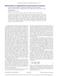
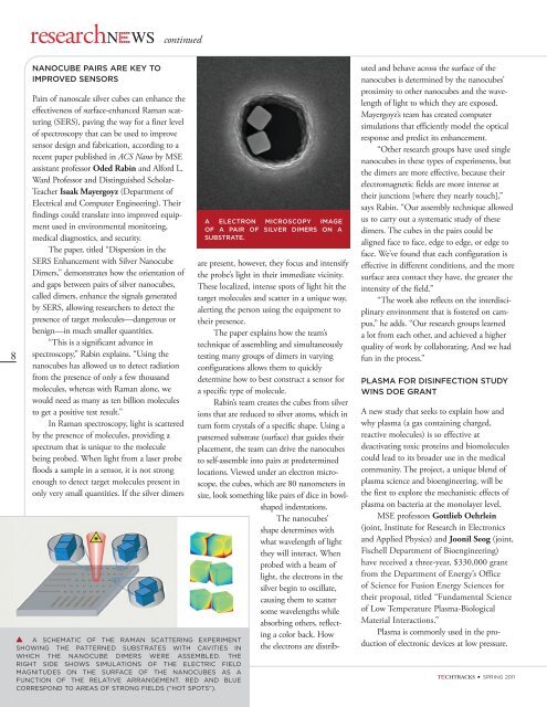
a schematic <strong>of</strong> the Raman scattering experiment<br />
showing the patterned substrates with cavities in<br />
which the nanocube dimers were assembled. The<br />
right side shows simulations <strong>of</strong> the electric field<br />
magnitudes on the surface <strong>of</strong> the nanocubes as a<br />
function <strong>of</strong> the relative arrangement. Red <strong>and</strong> blue<br />
correspond to areas <strong>of</strong> strong fields (“hot spots”).<br />
A electron microscopy image<br />
<strong>of</strong> a pair <strong>of</strong> silver dimers on a<br />
substrate.<br />
are present, however, they focus <strong>and</strong> intensify<br />
the probe’s light in their immediate vicinity.<br />
These localized, intense spots <strong>of</strong> light hit the<br />
target molecules <strong>and</strong> scatter in a unique way,<br />
alerting the person using the equipment to<br />
their presence.<br />
The paper explains how the team’s<br />
technique <strong>of</strong> assembling <strong>and</strong> simultaneously<br />
testing many groups <strong>of</strong> dimers in varying<br />
configurations allows them to quickly<br />
determine how to best construct a sensor for<br />
a specific type <strong>of</strong> molecule.<br />
Rabin’s team creates the cubes from silver<br />
ions that are reduced to silver atoms, which in<br />
turn form crystals <strong>of</strong> a specific shape. Using a<br />
patterned substrate (surface) that guides their<br />
placement, the team can drive the nanocubes<br />
to self-assemble into pairs at predetermined<br />
locations. Viewed under an electron microscope,<br />
the cubes, which are 80 nanometers in<br />
size, look something like pairs <strong>of</strong> dice in bowlshaped<br />
indentations.<br />
The nanocubes’<br />
shape determines with<br />
what wavelength <strong>of</strong> light<br />
they will interact. When<br />
probed with a beam <strong>of</strong><br />
light, the electrons in the<br />
silver begin to oscillate,<br />
causing them to scatter<br />
some wavelengths while<br />
absorbing others, reflecting<br />
a color back. How<br />
the electrons are distributed<br />
<strong>and</strong> behave across the surface <strong>of</strong> the<br />
nanocubes is determined by the nanocubes’<br />
proximity to other nanocubes <strong>and</strong> the wavelength<br />
<strong>of</strong> light to which they are exposed.<br />
Mayergoyz’s team has created computer<br />
simulations that efficiently model the optical<br />
response <strong>and</strong> predict its enhancement.<br />
“Other research groups have used single<br />
nanocubes in these types <strong>of</strong> experiments, but<br />
the dimers are more effective, because their<br />
electromagnetic fields are more intense at<br />
their junctions [where they nearly touch],”<br />
says Rabin. “Our assembly technique allowed<br />
us to carry out a systematic study <strong>of</strong> these<br />
dimers. The cubes in the pairs could be<br />
aligned face to face, edge to edge, or edge to<br />
face. We’ve found that each configuration is<br />
effective in different conditions, <strong>and</strong> the more<br />
surface area contact they have, the greater the<br />
intensity <strong>of</strong> the field.”<br />
“The work also reflects on the interdisciplinary<br />
environment that is fostered on campus,”<br />
he adds. “Our research groups learned<br />
a lot from each other, <strong>and</strong> achieved a higher<br />
quality <strong>of</strong> work by collaborating. And we had<br />
fun in the process.”<br />
Plasma for Disinfection Study<br />
Wins DOE Grant<br />
A new study that seeks to explain how <strong>and</strong><br />
why plasma (a gas containing charged,<br />
reactive molecules) is so effective at<br />
deactivating toxic proteins <strong>and</strong> biomolecules<br />
could lead to its broader use in the medical<br />
community. The project, a unique blend <strong>of</strong><br />
plasma science <strong>and</strong> bioengineering, will be<br />
the first to explore the mechanistic effects <strong>of</strong><br />
plasma on bacteria at the monolayer level.<br />
MSE pr<strong>of</strong>essors Gottlieb Oehrlein<br />
(joint, Institute for Research in Electronics<br />
<strong>and</strong> Applied Physics) <strong>and</strong> Joonil Seog (joint,<br />
Fischell Department <strong>of</strong> Bioengineering)<br />
have received a three-year, $330,000 grant<br />
from the Department <strong>of</strong> Energy’s Office<br />
<strong>of</strong> <strong>Science</strong> for Fusion Energy <strong>Science</strong>s for<br />
their proposal, titled “Fundamental <strong>Science</strong><br />
<strong>of</strong> Low Temperature Plasma-Biological<br />
Material Interactions.”<br />
Plasma is commonly used in the production<br />
<strong>of</strong> electronic devices at low pressure.<br />
TECHTRACKS <strong>Spring</strong> <strong>2011</strong>