ANSI/SCTE 16 2001R2007
ANSI/SCTE 16 2001R2007
ANSI/SCTE 16 2001R2007

You also want an ePaper? Increase the reach of your titles
YUMPU automatically turns print PDFs into web optimized ePapers that Google loves.
ENGINEERING COMMITTEE<br />
Interface Practices Subcommittee<br />
AMERICAN NATIONAL STANDARD<br />
<strong>ANSI</strong>/<strong>SCTE</strong> <strong>16</strong> <strong>2001R2007</strong><br />
Test Procedure for<br />
Hum Modulation
NOTICE<br />
The Society of Cable Telecommunications Engineers (<strong>SCTE</strong>) Standards are intended to serve the<br />
public interest by providing specifications, test methods and procedures that promote uniformity<br />
of product, interchangeability and ultimately the long term reliability of broadband<br />
communications facilities. These documents shall not in any way preclude any member or<br />
nonmember of <strong>SCTE</strong> from manufacturing or selling products not conforming to such documents,<br />
nor shall the existence of such standards preclude their voluntary use by those other than <strong>SCTE</strong><br />
members, whether used domestically or internationally.<br />
<strong>SCTE</strong> assumes no obligations or liability whatsoever to any party who may adopt the Standards.<br />
Such adopting party assumes all risks associated with adoption of these Standards or<br />
Recommended Practices, and accepts full responsibility for any damage and/or claims arising<br />
from the adoption of such Standards or Recommended Practices.<br />
Attention is called to the possibility that implementation of this standard may require use of<br />
subject matter covered by patent rights. By publication of this standard, no position is taken with<br />
respect to the existence or validity of any patent rights in connection therewith. <strong>SCTE</strong> shall not<br />
be responsible for identifying patents for which a license may be required or for conducting<br />
inquires into the legal validity or scope of those patents that are brought to its attention.<br />
Patent holders who believe that they hold patents which are essential to the implementation of<br />
this standard have been requested to provide information about those patents and any related<br />
licensing terms and conditions. Any such declarations made before or after publication of this<br />
document are available on the <strong>SCTE</strong> web site at http://www.scte.org.<br />
All Rights Reserved<br />
© Society of Cable Telecommunications Engineers, Inc. 2001, 2007<br />
140 Philips Road<br />
Exton, PA 19341<br />
i
Table of Contents<br />
1.0 Scope 1<br />
2.0 Definitions 1<br />
3.0 Background 1<br />
4.0 Equipment 2<br />
5.0 Setup 3<br />
6.0 1 dB Delta Measurement Procedure 6<br />
7.0 Differential Voltage Measurement Procedure 7<br />
Figure 1 Hum Modulation Test Setup 9<br />
Appendix 1 Hum Modulation Derivation 10<br />
Appendix 2 Derivation of the 100m VDC Delta Calibration 11<br />
Appendix 3 Conversion of the Hum Modulation from dB to percent (%) 12<br />
Table 1 Hum Modulation Conversion Chart 13<br />
Appendix 4 Time Domain vs. Frequency Domain Measurements 14<br />
Appendix 5 Hum Modulation Test Methods 15<br />
Appendix 6 Troubleshooting Guide 17<br />
Appendix 7 Special Test Conditions/Considerations 18<br />
ii
1.0 SCOPE<br />
To define and measure hum modulation in active and passive broadband RF telecommunications<br />
equipment and sub-assemblies. This procedure presents two methods for measuring hum<br />
modulation in the time domain, with a sensitivity exceeding -80 dB. These methods are referred<br />
to as the 1 dB delta and the differential voltage method. A mathematical relationship between<br />
time domain and frequency domain measurement methods is also provided.<br />
2.0 DEFINITIONS<br />
2.1. Hum Modulation: The amplitude distortion of a signal caused by the modulation of the<br />
signal with components of the power source. It is the ratio, expressed in dB, of the peak<br />
to peak variation of the carrier level caused by AC power line frequency products (and<br />
harmonics up to 1 kHz) to the peak voltage amplitude of the carrier.<br />
2.2. Peak Voltage Amplitude: The maximum voltage amplitude of the carrier.<br />
2.3. Percent Hum Modulation: Hum Modulation may also be expressed as a percentage of<br />
the peak to peak variation of the carrier level to the peak voltage amplitude of the<br />
carrier. See Appendix 3 for a derivation of percent Hum.<br />
3.0 BACKGROUND<br />
In a coaxial telecommunications system, where AC power and radio frequency (RF) signals exist<br />
on the same conductor, hum modulation of a television signal is measured as a comparison<br />
between the modulation envelope (created by line power distortions of the RF carriers), and the<br />
peak voltage of the sync tips of the video signal.<br />
In a laboratory test environment, the video signal is replaced with a sine wave RF carrier. Under<br />
these conditions, the only modulation existing on the carrier is the line power related distortion<br />
(created by the device under test) of that carrier. Hum modulation is determined as a function of<br />
the line frequency current passing through the device by comparing the peak to peak modulation<br />
envelope of the power line distortion to the peak voltage of the carrier by utilizing a diode<br />
detector.<br />
Due to the non-linear characteristics of any diode detector, it is inaccurate to simply compare the<br />
AC modulation voltage and the rectified DC carrier voltage directly due to the voltage drop<br />
across the diode. Instead, the modulation voltage is compared to a calibrated change in the<br />
rectified carrier.<br />
There are two time-domain methods for measuring hum modulation in a laboratory environment,<br />
which are detailed in this procedure. These methods are commonly referred to as the 1 dB delta<br />
method, and the differential voltage method. These methods are described in Appendix 5.<br />
1
4.0 EQUIPMENT<br />
4.1. The general equipment required for this test is shown in Figure 1. The Test Procedures<br />
Introduction document, <strong>ANSI</strong>/<strong>SCTE</strong> 96 2004, describes and specifies this equipment.<br />
4.2 The signal generator for this test must have (minimum) the characteristics listed below.<br />
4.2.1 5 MHz – 1.002 GHz (minimum) single carrier signal generation<br />
capability.<br />
4.2.2 0.2% minimum AM modulation index capability.<br />
4.2.3 < 0.01% residual hum.<br />
4.2.4 Suggested Equipment: Hewlett Packard ESG-4000A Signal Generator or<br />
equivalent.<br />
4.3 Two AC/RF Power Combiners/Inserters:<br />
4.3.1 Hum modulation < -80 dB at desired test current and voltage.<br />
4.3.2 Return loss: > 22 dB.<br />
4.3.3 Power Combiners/Inserters must possess RF only input/output capability,<br />
i.e. AC blocking incorporated into design.<br />
4.3.4 Current carrying capacity of at least 50% greater than desired test currents.<br />
Note: AC/RF Power Combiners/Inserters may not be required for certain DUT<br />
applications. Refer to Appendix 7 for special test considerations.<br />
4.4 Resistive Load Bank: capable of dissipating desired test power.<br />
4.5 Display Devices:<br />
4.5.1 Power analyzer capable of measuring rms current and voltage<br />
simultaneously.<br />
4.5.2 Oscilloscope must have a minimum deflection sensitivity of 2.0 mV/div.<br />
4.5.2.1 Suggested Equipment: Tektronix TDS724A Digitizing<br />
Oscilloscope with Tektronix ADA400A Differential Preamplifier<br />
or equivalent (recommended, preamplifier not used in<br />
differential mode).<br />
4.5.2.2 The oscilloscope used for the test must possess signal averaging<br />
capability.<br />
4.6 Power supply:<br />
4.6.1 Ferro-resonant quasi-square wave (trapezoidal wave with < 100 V/ms<br />
slew rate).<br />
4.6.2 AC voltage output (50/60 Hz) at desired test voltage.<br />
4.6.3 Rated current output of at least 30% greater than the desired test current.<br />
4.7 Low Pass Filter: DC – 1 kHz(minimum)<br />
4.7.1 Shielded.<br />
4.7.2 High Impedance (5 kΩ or greater).<br />
2
4.7.3 > 30 dB attenuation above 30 kHz.<br />
4.7.4 This filter may be contained in the differential preamplifier used in the<br />
test.<br />
4.8 AM Detector:<br />
4.8.1 75 Ω Input Impedance.<br />
4.8.2 Frequency Range: 200 kHz to 1.002 GHz.<br />
4.8.3 Maximum VSWR: 1.2:1 to 1.002 GHz.<br />
4.8.4 Suggested Equipment: Trilithic CD-75 or equivalent.<br />
4.9 Required inter-connect cables and connectors.<br />
4.9.1 Quad-shield 75Ω coaxial cable, for RF only paths.<br />
4.9.2 Rigid or semi-rigid 75Ω coaxial cable (1/2” diameter or greater), for RF<br />
and AC common paths, with a current carrying capacity of at least 50%<br />
greater than desired test currents.<br />
4.9.3 Suggested Equipment: Gilbert interconnect cables or equivalent.<br />
4.10 Isolation Transformer<br />
4.10.1 115 – 120 VAC Input : 115 – 120 VAC Output.<br />
4.10.2 50/60 Hz.<br />
4.10.3 > 1,000 VA.<br />
4.10.4 Suggested Equipment: Xentek EIT 1.0-31<br />
4.11 RF Amplifier<br />
4.11.1 5 MHz – 1 GHz (two amplifiers may be used to encompass this frequency<br />
range).<br />
4.11.2 Gain ≅ 25 dB.<br />
4.11.3 Noise Figure ≤ 10 dB.<br />
4.12 RF Attenuators<br />
4.12.1 Maximum VSWR: 1.2:1 to 1 GHz.<br />
4.12.2 75 Ω Switchable Attenuators.<br />
4.12.2.1 0.1 dB steps, 0 – 1 dB range, ±0.05 dB tolerance.<br />
4.12.2.2 1.0 dB steps, 0 – 10 dB range, ±0.1 dB tolerance.<br />
4.12.2.3 10.0 dB steps, 0 – 70 dB range, ±0.2 dB tolerance.<br />
4.12.3 75 Ω fixed attenuators: 10 dB values, ±0.05 dB tolerance.<br />
5.0 SETUP<br />
5.1. Follow all calibration requirements recommended by the manufacturers of the test<br />
equipment, including adequate warm-up and stabilization time.<br />
5.2. Connect the test equipment as shown in Figure 1.<br />
Note: AC/RF Power Combiners/Inserters may not be required for certain DUT applications.<br />
Refer to Appendix 7 for special test considerations.<br />
3
5.3. Set the oscilloscope to the following settings:<br />
Vertical Scale<br />
Horizontal Scale<br />
Input Impedance<br />
AC Coupled Mode<br />
Measurement Mode<br />
Signal Averaging<br />
Trigger<br />
As required for waveform<br />
display<br />
1 ms/div<br />
1 MΩ<br />
On<br />
V pk-pk<br />
Off<br />
External<br />
Note: A pre-amplifier is recommended to increase the vertical resolution of the oscilloscope, and<br />
extend the noise floor.<br />
5.4. Determine RF levels:<br />
5.4.1. Connect DUT into test setup.<br />
5.4.2. Set the signal generator to a frequency within the operating range of the device.<br />
5.4.3. Adjust the signal generator RF output level, while monitoring the RF test point, to<br />
set the RF output level of the DUT to it’s typical operating levels.<br />
5.4.4. Adjust the step attenuator preceding the RF post amplifier until the voltmeter<br />
displays approximately 0.9 VDC. If this voltage cannot be obtained, the gain of the<br />
RF post amp will need to be increased. This will ensure operation in the linear<br />
region of the AM detector.<br />
Note: Section 5.4 establishes the calibration voltage while maintaining the DUT at it’s rated<br />
output level (achieved by monitoring the test point). This prevents possible compression of the<br />
DUT while obtaining the calibration voltage.<br />
5.5. Calibration:<br />
5.5.1. Add 1.0 dB of attenuation from the input attenuator and note the voltage change<br />
on the voltmeter.<br />
5.5.2. Fine tune the amplitude of the signal generator until a 1.0 dB switchable<br />
attenuator change causes a 100 mVDC deflection on the voltmeter. When a 100<br />
mVDC delta is achieved, record the DC voltage at the higher signal level as the<br />
detector dc operating point or calibration voltage.(see Appendix 2)<br />
4
5.6. Calibration verification:<br />
5.6.1. AM modulate the signal generator at 0.5%(conventional AM index), 400 Hz.<br />
5.6.2. Adjust oscilloscope for maximum signal deflection, then measure V p-p and signal<br />
period. With the pre-amplifier gain set to 100, a sinusoidal signal with a period of<br />
2.5 ms (400 Hz) and amplitude of approximately 900 mV should appear on the<br />
oscilloscope if the setup is properly calibrated. This corresponds to a hum<br />
modulation of 1.0% or -40 dB (see section 5.7 and Appendix 2 for calculations).<br />
5.6.3. Turn off signal generator AM modulation.<br />
5.7. AC Power Combiner Back-to-Back Hum Modulation Characterization:<br />
5.7.1. Remove the DUT and install a calibration jumper as shown in Figure 1. A cable<br />
or adapter may be used in place of the DUT, when applicable.<br />
5.7.2. Turn on AC power supply and adjust load bank to desired test current, as<br />
displayed on power analyzer.<br />
5.7.3. Set signal generator to desired test frequency.<br />
5.7.4. Set-up the oscilloscope:<br />
Horizontal Scale<br />
Trigger<br />
Signal Averaging<br />
5 ms/div<br />
Line<br />
Off<br />
5.7.5. Adjust RF amplitude at the generator until the voltmeter displays the calibration<br />
voltage determined in section 5.5.2, above. Record this voltage in millivolts as<br />
V a .<br />
5.7.6. Adjust the oscilloscope for maximum deflection of the non-averaged signal,<br />
making sure that none of the signal amplitude goes off-screen.<br />
5.7.7. Set signal averaging to 64 samples or greater.<br />
5.7.8. Record the peak-to-peak voltage of the hum modulation waveform as mV p-p in<br />
millivolts after the averaging has settled.<br />
5.7.9. Add 1 dB of attenuation at the generator output or decrease the signal generator<br />
level by 1 dB and record the DC voltage in millivolts displayed by the voltmeter<br />
as V b .<br />
5.7.10. Calculate noise floor hum in dB as:<br />
Hum (dB) = -19.27 –20Log(V a -V b ) + 20Log(mV p-p /100) (See Appendix 2 for<br />
derivation)<br />
5
Note: The mV p-p value must be divided by 100 due to the pre-amplifier gain. If the preamplifier<br />
is not used, the mV p-p value is divided by 1.<br />
5.7.11. Calculate hum in percent as:<br />
Hum (%) = 100 * 10 Hum(dB)/20<br />
(See Appendix 3 for derivation)<br />
5.7.12. Repeat steps 5.7.3 through 5.7.11 for all test frequencies.<br />
5.7.13. Turn off power supply and remove calibration jumper.<br />
5.7.14. Turn off signal generator RF output.<br />
Note: The back-to-back hum modulation of the power combiners should be a minimum of<br />
–75 dB, with a goal of greater than –80 dB. If the noise floor is not lower than –75 dB, there<br />
may be a ground loop in the AC circuit. See Appendix 6 for ground loop trouble shooting<br />
recommendations.<br />
6.0 1 dB DELTA MEASUREMENT PROCEDURE<br />
6.1 Connect DUT into test setup.<br />
.<br />
6.2 Turn on power supply and load to desired test current (using the resistive load bank) as<br />
measured on the power analyzer.<br />
6.3 Operate the DUT under power until it reaches temperature stability.<br />
6.4 Set signal generator to desired test frequency and turn RF on.<br />
6.5 Adjust RF amplitude at the generator until the voltmeter displays the calibration voltage<br />
determined in section 5.5.2, above. Record this voltage as V a . (in mV)<br />
6.6. Adjust the oscilloscope for maximum deflection of the non-averaged signal, making sure<br />
that none of the signal amplitude goes off-screen.<br />
6.7. Set signal averaging to 64 samples or greater.<br />
6.8. Record the peak-to-peak voltage of the hum modulation waveform as mV p-p in millivolts<br />
after the averaging has settled.<br />
Note: When using signal averaging, make sure that the non-averaged signal does not go off<br />
the screen when adjusting the oscilloscope for maximum deflection. This can cause severe<br />
averaging errors.<br />
6.9. Decrease the signal generator level by 1.0 dB and record the DC voltage displayed by<br />
the voltmeter as V b . (in mV)<br />
6
6.10. Calculate hum in dB as:<br />
Hum (dB) = -19.27 –20Log(V a -V b ) + 20Log(mV p-p /100). (See Appendix 2 for<br />
derivation)<br />
Note: The mV p-p value must be divided by 100 due to the pre-amplifier gain. If the pre-amp is<br />
not used, the mV p-p value is divided by 1.<br />
6.11. Calculate hum in percent as: Hum (%) =100 * 10 Hum(dB)/20 .(See Appendix 3 for<br />
derivation)<br />
6.12. Repeat steps 6.4 through 6.11 for all test frequencies and temperatures.<br />
7.0 DIFFERENTIAL VOLTAGE MEASUREMENT PROCEDURE<br />
7.1 Connect DUT into test setup.<br />
7.2 Turn on power supply and load to desired test current (using the resistive load bank) as<br />
measured on the power analyzer.<br />
7.3 Operate the DUT under power until it reaches temperature stability.<br />
7.4 Set signal generator to desired test frequency and turn RF on.<br />
7.5 Adjust RF amplitude at the generator until the voltmeter displays the calibration<br />
voltage determined in section 5.5.2, above.<br />
Note: The signal generator level can be adjusted to levels less than the calibration voltage<br />
without loss of accuracy to accommodate measurements such as a sloped frequency response at<br />
the DUT output. The generator level does not need to be adjusted at each frequency if the<br />
calibration voltage is not exceeded during the test sequence.<br />
7.6 AM modulate the signal generator to 0.5 % (conventional AM index) at 400 Hz.<br />
7
7.7 Set the oscilloscope to the following settings:<br />
Vertical Scale<br />
Horizontal Scale<br />
Measurement Mode<br />
AC Coupled Mode<br />
Signal Averaging<br />
Trigger<br />
As required for waveform<br />
display<br />
1 ms/div<br />
V pk-pk<br />
On<br />
> 64 Samples<br />
External<br />
Note: Reliable triggering of the oscilloscope is obtained through a direct connection between the<br />
signal generator modulation test point and the oscilloscope external trigger. Do not make a<br />
ground connection between the signal generator and oscilloscope through this cable as this will<br />
cause ground loop hum.<br />
7.8 The oscilloscope should display the reference modulation envelope. Record the peak to<br />
peak amplitude value as V ref in mV p-p when the averaging has settled.<br />
7.9 Turn off signal generator AM modulation.<br />
7.10 Change the following oscilloscope settings:<br />
Horizontal Scale<br />
Trigger<br />
5 ms/div<br />
Line<br />
7.11 Adjust the oscilloscope for maximum deflection of the displayed signal and record the<br />
peak to peak amplitude value as V hum in mV p-p when the averaging has settled.<br />
Note: When using signal averaging, make sure that the non-averaged signal does not go off the<br />
screen when adjusting the oscilloscope for maximum deflection. This can cause severe<br />
averaging errors.<br />
7.12 Calculate hum in dB as: Hum (dB) = -40.04 –20Log(V ref ) + 20Log(V hum ). (See<br />
Appendix 5 for derivation.)<br />
7.13 Calculate hum in % as: Hum (%) = 100 * 10 Hum(dB)/20 . (See Appendix 3 for derivation.)<br />
7.14 Repeat steps 7.4 through 7.13 for all test frequencies and temperatures.<br />
8
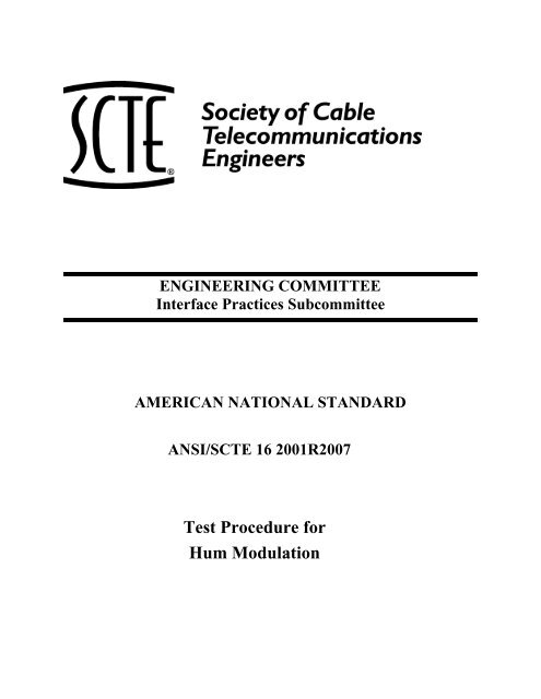
Hum Modulation Test Setup<br />
Signal Generator<br />
Isolation<br />
Transformer<br />
Step<br />
(Optional)<br />
DC-<strong>16</strong> (RF Test Point)<br />
Attenuator<br />
10dB<br />
Pad<br />
RF<br />
Power<br />
Inserter<br />
(AC Blocking)<br />
RF+AC<br />
DUT<br />
RF+AC<br />
RF<br />
Power Inserter<br />
(AC Blocking)<br />
10dB<br />
Pad<br />
Step<br />
Attenuator<br />
RF Amp<br />
AC<br />
Power Analyzer<br />
AC<br />
AC<br />
Load Bank.<br />
SLM<br />
AM Detector<br />
Power Supply<br />
AC<br />
Calibration<br />
Jumper<br />
Isolation<br />
Transformer<br />
(Optional)<br />
Volt Meter<br />
LPF<br />
GFCI<br />
AC<br />
Isolation<br />
Transformer<br />
Oscilloscope<br />
Pre-<br />
Amplifier<br />
(Optional)<br />
Figure 1<br />
10
Appendix 1 – Hum Modulation Derivation<br />
The equation for a TV sinewave amplitude modulated carrier is:<br />
y(t) = B[1 − (k / 2)(1 + cosω m t)]cosω<br />
c<br />
t<br />
(A -1)<br />
where B is the peak amplitude of the RF carrier and k is the modulation factor which is equal to:<br />
M pk−pk<br />
k = , k ≤ 1<br />
B<br />
and k is related to the conventional AM modulation index by the equation:<br />
(A - 2)<br />
k =<br />
2m<br />
( 1+<br />
m)<br />
where m is the conventional AM modulation index.<br />
If the peak-to-peak amplitude variation in time is kB, and this amplitude variation is considered<br />
to be hum modulation, hum is defined as.<br />
AM Mod(dB) = 20Log =<br />
B<br />
( kB ) 20Log( k) (A<br />
Hum modulation is simply a measurement of k, which is the ratio of the peak-to-peak hum on the<br />
carrier to the peak of the RF carrier (B).<br />
- 3)<br />
k =<br />
Hum<br />
B<br />
pk−pk<br />
(A - 4)<br />
Figure 2 shows a graphical representation of hum modulation using a continuous wave (CW)<br />
carrier as an example.<br />
Hum pk-pk<br />
V peak (Peak Voltage of RF Carrier)<br />
Carrier Voltage<br />
Time<br />
Figure 2<br />
11
Appendix 2 – Derivation of the 100mVDC Delta Calibration<br />
The 100mVDC delta hum modulation reference calibration procedure establishes, through a –1<br />
dB RF level change, a repeatable envelope change that can be compared to the actual peak-topeak<br />
hum voltage. From this a hum modulation ratio can be determined.<br />
Consider the signal:<br />
v(t)<br />
= B 1<br />
[ − v (t)] cos ω t<br />
(A - 5)<br />
hum<br />
Where B is the peak amplitude of the RF carrier, v hum (t) is the peak-to-peak hum voltage, and B<br />
in dB is defined as B(dB) = 20Log(B/B o ). If B is attenuated by 1 dB (which corresponds to a<br />
100 mVDC delta on the voltmeter), then:<br />
−1dB<br />
= 20Log B @ −1dB<br />
/ Bo<br />
So,<br />
ΔB @ −1dB,100mV<br />
= B − B<br />
c<br />
( ( ) ) (A - 6)<br />
( −1/<br />
20) ( −1/<br />
20)<br />
( ) • 10 = B ( 1−10<br />
)<br />
p−p<br />
Time domain hum modulation can be defined as:<br />
O<br />
O<br />
O<br />
V<br />
p−p<br />
(A - 7)<br />
Env<br />
Hum(dB) = 20Log<br />
⎡<br />
⎢⎣<br />
max<br />
− Env<br />
min<br />
Env<br />
max<br />
⎤<br />
⎥⎦<br />
(A - 8)<br />
Where Env max is the –1 dB delta in B (envelope change) that can be compared to the actual peakto-peak<br />
hum voltage (Env max -Env min ) to give a hum modulation ratio in dB.<br />
[ ΔB (@<br />
−1dB,<br />
0.1Vp<br />
−p<br />
)]<br />
[ ]<br />
(A - 9)<br />
Env max =<br />
( −1/<br />
20<br />
1−10<br />
)<br />
Env<br />
max<br />
− Env<br />
min<br />
= Hum<br />
p−p<br />
(A -10)<br />
At the 100mVDC calibration reference (which is a 100 mV p-p delta envelope reference), the<br />
equation for hum modulation is:<br />
( −1/<br />
20)<br />
⎡Hum<br />
Hum(dB) = 20Log(1 −10<br />
) + 20Log⎢<br />
⎣<br />
mVp−p<br />
100mV<br />
p−p<br />
⎤<br />
ref ⎥<br />
⎦<br />
(A -11)<br />
Where Hum p-p is given in millivolts, and hum modulation is given in dB.<br />
Hum(dB)<br />
= −19.27<br />
− 20Log 100mV<br />
( ref ) + 20Log(Hum ) = −59.27<br />
20Log( Hum ) (A -12)<br />
p− p<br />
mVp−p<br />
+<br />
mVp−p<br />
12
Appendix 3 – Conversion of Hum Modulation from dB to percent (%)<br />
The Federal Communications Commission (FCC) defines hum in Technical Standards part<br />
76.605(a) as: The peak to peak variation in visual signal level caused by undesired low<br />
frequency disturbances (hum or repetitive transients) generated within the system, or by<br />
inadequate low frequency response, shall not exceed 3 percent of the visual signal level.<br />
This appendix will detail the derivation of hum modulation in percent, and will provide a table<br />
with conversions of hum modulation from mV p-p to dB and percent hum.<br />
Hum Modulation may be expressed as a percentage of the peak to peak variation of the carrier<br />
level to the peak voltage amplitude of the carrier. From equations A-9 and A-10, located in<br />
Appendix 2, Env max is defined as the –1 dB delta in B (envelope change) that can be compared to<br />
the actual peak to peak hum voltage (Env max - Env min , or Hum p-p ) to give a hum modulation ratio.<br />
To express hum modulation as a percent:<br />
Hum(%)<br />
⎛ HummVp−p<br />
⎞ ⎛ HummVp−p<br />
⎞<br />
= ⎜ ⎟ *100% ⎜<br />
⎟<br />
*100% = .109* HummVp−p<br />
Env<br />
=<br />
(A-13)<br />
max<br />
919.5mV<br />
⎝ ⎠ ⎝<br />
p−p<br />
⎠<br />
where,<br />
Env<br />
max<br />
100mV 100mV<br />
= (from A-9)<br />
p−p<br />
p−p<br />
( 20)<br />
p p<br />
[ ] 1/ = = 919.5mV<br />
−<br />
−<br />
1−10<br />
.1087<br />
The 100mV delta is shown as the standard reference. However, for hum measurements, the<br />
actual delta of voltages between the 1 dB change should be used for improved accuracy.<br />
The conversion of hum in mV p-p to dB and percent is shown in Table 1.<br />
13
Table 1<br />
Hum Modulation Conversion Chart<br />
mV p-p dB % mV p-p dB % mV p-p dB %<br />
0.082 81.0 0.0089 0.774 61.5 0.0843 7.303 42.0 0.7960<br />
0.087 80.5 0.0095 0.819 61.0 0.0893 7.736 41.5 0.8432<br />
0.092 80.0 0.0100 0.868 60.5 0.0946 8.194 41.0 0.8932<br />
0.097 79.5 0.0106 0.919 60.0 0.1002 8.680 40.5 0.9461<br />
0.103 79.0 0.0112 0.974 59.5 0.1062 9.194 40.0 1.0021<br />
0.109 78.5 0.0119 1.032 59.0 0.1124 9.739 39.5 1.0615<br />
0.1<strong>16</strong> 78.0 0.0126 1.093 58.5 0.1191 10.3<strong>16</strong> 39.0 1.1244<br />
0.123 77.5 0.0134 1.157 58.0 0.1262 10.927 38.5 1.1910<br />
0.130 77.0 0.0142 1.226 57.5 0.1336 11.574 38.0 1.26<strong>16</strong><br />
0.138 76.5 0.0150 1.299 57.0 0.14<strong>16</strong> 12.260 37.5 1.3364<br />
0.146 76.0 0.0159 1.376 56.5 0.1499 12.987 37.0 1.4156<br />
0.154 75.5 0.0<strong>16</strong>8 1.457 56.0 0.1588 13.756 36.5 1.4994<br />
0.<strong>16</strong>3 75.0 0.0178 1.543 55.5 0.<strong>16</strong>82 14.571 36.0 1.5883<br />
0.173 74.5 0.0189 1.635 55.0 0.1782 15.435 35.5 1.6824<br />
0.183 74.0 0.0200 1.732 54.5 0.1888 <strong>16</strong>.349 35.0 1.7821<br />
0.194 73.5 0.0212 1.834 54.0 0.2000 17.318 34.5 1.8877<br />
0.206 73.0 0.0224 1.943 53.5 0.2118 18.344 34.0 1.9995<br />
0.218 72.5 0.0238 2.058 53.0 0.2244 19.431 33.5 2.1180<br />
0.231 72.0 0.0252 2.180 52.5 0.2376 20.583 33.0 2.2435<br />
0.245 71.5 0.0267 2.309 52.0 0.2517 21.802 32.5 2.3764<br />
0.259 71.0 0.0282 2.446 51.5 0.2666 23.094 32.0 2.5173<br />
0.274 70.5 0.0299 2.591 51.0 0.2824<br />
0.291 70.0 0.0317 2.745 50.5 0.2992<br />
0.308 69.5 0.0336 2.907 50.0 0.3<strong>16</strong>9<br />
0.326 69.0 0.0356 3.080 49.5 0.3357<br />
0.346 68.5 0.0377 3.262 49.0 0.3556<br />
0.366 68.0 0.0399 3.455 48.5 0.3766<br />
0.388 67.5 0.0423 3.660 48.0 0.3990<br />
0.411 67.0 0.0448 3.877 47.5 0.4226<br />
0.435 66.5 0.0474 4.107 47.0 0.4476<br />
0.461 66.0 0.0502 4.350 46.5 0.4742<br />
0.488 65.5 0.0532 4.608 46.0 0.5023<br />
0.517 65.0 0.0564 4.881 45.5 0.5320<br />
0.548 64.5 0.0597 5.170 45.0 0.5635<br />
0.580 64.0 0.0632 5.476 44.5 0.5969<br />
0.614 63.5 0.0670 5.801 44.0 0.6323<br />
0.651 63.0 0.0709 6.145 43.5 0.6698<br />
0.689 62.5 0.0751 6.509 43.0 0.7095<br />
0.730 62.0 0.0796 6.894 42.5 0.7515<br />
Hum (dB) = -59.27 + 20 Log (Hum mVp-p )<br />
Hum (%) = 0.109 * Hum mVp-p<br />
14
Appendix 4 – Time domain vs. Frequency domain Measurements<br />
This appendix is intended to demonstrate a mathematical correlation between the time<br />
domain measurement method (which this procedure details), and the frequency domain<br />
measurement method. The frequency domain method uses a spectrum analyzer as a tuned<br />
receiver to demodulate the 60, 120, or 180 Hz hum sidebands to baseband for measurement with<br />
a low frequency spectrum analyzer. This measurement technique is seldom used as it requires a<br />
spectrum analyzer with 10Hz or better resolution.<br />
Before a correlation between the two measurement methods is shown, the equations for<br />
conventional AM and TV AM should be reviewed.<br />
Conventional AM:<br />
x(t)<br />
= A 1<br />
[ + m( cosω m t)<br />
] cosω<br />
t<br />
(A -14)<br />
Where A is the carrier and m is the conventional modulation index. The equation for TV AM<br />
(A-1) is located in Appendix 1. If these equations are converted to show the AM sidebands:<br />
Conventional AM:<br />
⎡<br />
x( t)<br />
= A<br />
⎢<br />
cosω<br />
⎣<br />
c<br />
t +<br />
1<br />
2<br />
c<br />
[ ( ω − ω ) t + cos( ω + ω ) t] (A -15)<br />
m cos<br />
c<br />
m<br />
c<br />
m<br />
⎥ ⎦<br />
⎤<br />
TV AM:<br />
⎡<br />
y(t)<br />
= B<br />
⎢<br />
1−<br />
⎣<br />
k<br />
4<br />
[ ( k / 2)<br />
] cosω<br />
t − [ cos( ω − ω ) t + cos( ω + ω ) t] (A -<strong>16</strong>)<br />
c<br />
c<br />
m<br />
It can be determined from these equations that for conventional AM signals, the AM sidebands<br />
are m/2 volts(assuming that carrier A is 1 volt). For TV AM, the sidebands are k/4 volts(also<br />
assuming that carrier B is 1 volt). Appendix 1, through mathematical derivation, shows that<br />
Hum(dB) = 20Log(k). If the frequency domain method is used to measure the sideband, the<br />
equation becomes:<br />
Hum(dB)<br />
= 20Log<br />
Therefore, for frequency domain measurements, a correction factor of 12 dB must be subtracted<br />
from the measurement to correlate to the time domain measurement method.<br />
c<br />
( k ) = 20Log(k) − 20Log4 = 20log(k) −12<br />
(A -17)<br />
4<br />
m<br />
⎥ ⎦<br />
⎤<br />
15
Appendix 5: Hum Modulation Test Methods<br />
Note that both of the time-domain methods detailed in the procedure depend upon the<br />
comparison of an unknown envelope to a known calibrated envelope. The difference between<br />
the two methods lies in the way the reference envelope is established and measured. The general<br />
principles of hum modulation measurement are covered in Appendix 1.<br />
1 dB Delta Method<br />
The 1 dB delta method creates a standard reference envelope by switching a 1 dB attenuator<br />
in the signal line to the device under test, and calibrates the amplitude of this 1 dB envelope by<br />
measuring the rectified DC component of the carrier with a digital voltmeter. The oscilloscope<br />
is not involved in this calibration. This procedure presumes that a large signal DC measurement<br />
correlates to a small signal AC measurement using a different instrument, and it presumes that<br />
the AC/DC characteristics of the detector are constant for all test frequencies. The derivation of<br />
the formula for hum modulation using this method is found in Appendix 2.<br />
The accuracy of this method is influenced by the accuracy of the 1 dB attenuation, the<br />
frequency and signal level response of the AM detector, the gain of the differential amplifier,<br />
and the correlation of the measurement instruments measuring different signal components. This<br />
kind of instrument diversity makes this an absolute measurement.<br />
Differential Voltage Method<br />
The differential voltage method creates a standard reference envelope by deploying the<br />
internal AM modulation function of the generator as described in 5.6 to establish calibration<br />
verification. This reference modulation envelope is measured as a peak to peak AC voltage<br />
waveform on the oscilloscope in the same way that the hum modulation waveform is measured<br />
using the same measurement instrument. The rectified DC component of the signal does not<br />
enter into the measurement, therefore, the detector response with respect to frequency does not<br />
affect the measurement. Likewise, the gain and insertion loss accuracy in the signal path does<br />
not influence the result because it is common to both the reference and the test measurement.<br />
The accuracy of this method is influenced by the calibration of the modulation index of<br />
the internal modulation generator, and the vertical range selector of the oscilloscope. This kind<br />
of instrument commonality makes this a releative measurement.<br />
In establishing a relation between the hum waveform and the peak carrier level, an<br />
intermediate reference waveform is used which has a known relationship to the carrier by virtue<br />
of its modulation index. From Appendix 1, the relationship of a conventional AM modulation<br />
envelope defined by its modulation index m, to the peak carrier amplitude B is given by:<br />
AM mod(dB) = 20Log<br />
( kB<br />
2m<br />
) = 20Log( k) , where k =<br />
(A - 3)<br />
B<br />
1+<br />
m<br />
<strong>16</strong>
The relationship of the peak to peak hum waveform to the peak to peak reference modulation is<br />
simply:<br />
⎛ V ⎞<br />
⎜<br />
hum<br />
20 Log<br />
⎟ as measured on the oscilloscope. (A – 18)<br />
⎝ Vref<br />
⎠<br />
Combining these two relationships, the peak to peak hum is related to the peak carrier by:<br />
⎛ V ⎞<br />
⎜<br />
hum<br />
Hum (dB) = 20Log(k) + 20Log<br />
⎟ or (A – 19)<br />
⎝ Vref<br />
⎠<br />
Hum(dB)<br />
= 20Log(k) − 20Log(V ) 20Log(V ) . (A – 20)<br />
ref +<br />
A convenient modulation index to use is 0.5% AM. If this value is substituted for m, the first<br />
term in equation A-20 becomes –40.04 dB. If a higher degree of accuracy is required, the<br />
modulation index can be empirically determined by measuring the carrier and its sidebands<br />
across the test spectrum. From HP application note #150-1, the relationship between the<br />
logarithmic display and the modulation percentage is expressed as:<br />
(dB)<br />
E −E<br />
C(dB)<br />
+ 6) / 20<br />
hum<br />
20log m = E SB − E + 6dB (A - 21)<br />
(<br />
C<br />
SB<br />
m = 10<br />
(A – 22)<br />
17
Appendix 6: Troubleshooting Guide<br />
This appendix will serve as a guide to eliminate AC ground loops in the hum modulation test<br />
setup. Identification of a ground loop problem will normally be made when measuring the backto-back<br />
hum modulation of the power combiners. If the noise floor is not lower than –75 dB, the<br />
setup should be investigated for possible contribution to the noise floor.<br />
General Troubleshooting<br />
If the noise floor goal cannot be met, take the following steps to determine if the test<br />
equipment/test setup is contributing to the problem:<br />
1. Ensure all test equipment is set to the operating parameters detailed in this procedure.<br />
2. Ensure all connectors and cables used in the test setup are correctly constructed and firmly<br />
connected. Light shaking or tapping on each connector can help to identify a potential<br />
problem.<br />
3. Ensure the hum power combiners are constructed properly; i.e. check for poor solder<br />
connections, etc…<br />
Ground Loop Elimination<br />
If the conditions in the general troubleshooting guide are met, an AC ground loop is most<br />
likely the cause of the poor noise floor measurements. The following steps may be taken to<br />
prevent or eliminate these ground loops.<br />
1. Utilize a power bar (driven from an isolation transformer) with the common ground removed<br />
on each piece of test equipment (signal generator, oscilloscope, and voltmeter).<br />
2. Isolation plugs (2 – 3 prong adapter type) should be used on each piece of test equipment.<br />
3. Ensure that any plug outlet being used for the test is not introducing any 60 Hz hum to the<br />
system.<br />
4. Avoid multiple ground paths between equipment such as the signal generator and the<br />
oscilloscope. A cable connecting the generator modulation test point to the oscilloscope<br />
external trigger must not have a complete ground path<br />
5. Special Consideration: If the test setup is automated, ground loops can occur between the PC<br />
and any test equipment via the instrument interface bus. Bus opto-isolators can be utilized to<br />
eliminate this problem.<br />
18
Appendix 7 – Special Test Conditions/Considerations<br />
The test setup and procedure in this document detail a test methodology that is specific to<br />
devices in which the power enters and exits on the RF test ports. However, some test devices do<br />
not contain this configuration. Drop amplifiers are an example of a device that does not contain<br />
two RF/power ports. Typical configurations of drop amplifiers include use of only one<br />
RF/power port, or a dedicated power port and stand alone (no power passing capability) RF<br />
ports.<br />
Under circumstances such as the ones listed above, this procedure can be followed with minor<br />
test set-up modifications. If one or more RF ports of the DUT do not contain power passing<br />
capability, AC/RF power inserters/combiners are not required for those ports. They may be<br />
removed for testing purposes.<br />
For example, a DUT containing only one RF/power port would be tested using one AC/RF<br />
power inserter/combiner on the RF/power port, and an RF only connection on the other port. A<br />
DUT containing a dedicated powering port would not require AC/RF power inserters/combiners<br />
on the test ports, as they are not meant to pass power.<br />
A general rule of thumb when performing this test is to utilize AC/RF power inserters/combiners<br />
on any DUT port that shares RF and power passing capability. Otherwise, direct connections<br />
should be used. Additionally, the power load bank is not required on DUT’s without power<br />
passing capability. The procedure can be followed as stated with these minor changes to the test<br />
set-up.<br />
19