Scenix - Futura Elettronica
Scenix - Futura Elettronica
Scenix - Futura Elettronica

Create successful ePaper yourself
Turn your PDF publications into a flip-book with our unique Google optimized e-Paper software.
www.scenix.com<br />
Chapter 1 Overview<br />
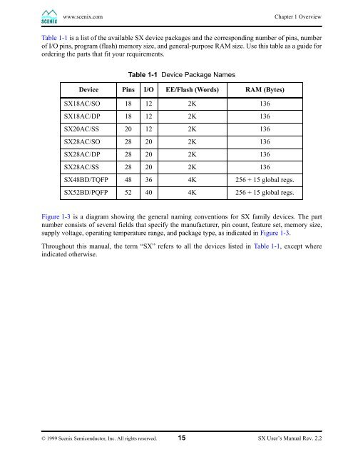
Table 1-1 is a list of the available SX device packages and the corresponding number of pins, number<br />
of I/O pins, program (flash) memory size, and general-purpose RAM size. Use this table as a guide for<br />
ordering the parts that fit your requirements.<br />
Table 1-1 Device Package Names<br />
Device Pins I/O EE/Flash (Words) RAM (Bytes)<br />
SX18AC/SO 18 12 2K 136<br />
SX18AC/DP 18 12 2K 136<br />
SX20AC/SS 20 12 2K 136<br />
SX28AC/SO 28 20 2K 136<br />
SX28AC/DP 28 20 2K 136<br />
SX28AC/SS 28 20 2K 136<br />
SX48BD/TQFP 48 36 4K 256 + 15 global regs.<br />
SX52BD/PQFP 52 40 4K 256 + 15 global regs.<br />
Figure 1-3 is a diagram showing the general naming conventions for SX family devices. The part<br />
number consists of several fields that specify the manufacturer, pin count, feature set, memory size,<br />
supply voltage, operating temperature range, and package type, as indicated in Figure 1-3.<br />
Throughout this manual, the term “SX” refers to all the devices listed in Table 1-1, except where<br />
indicated otherwise.<br />
© 1999 <strong>Scenix</strong> Semiconductor, Inc. All rights reserved. 15 SX User’s Manual Rev. 2.2