NPN RF Amplifier Transistor Surface Mount MSC3130T1 - Datasheets
NPN RF Amplifier Transistor Surface Mount MSC3130T1 - Datasheets
NPN RF Amplifier Transistor Surface Mount MSC3130T1 - Datasheets

Create successful ePaper yourself
Turn your PDF publications into a flip-book with our unique Google optimized e-Paper software.
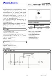
SEMICONDUCTOR TECHNICAL DATA<br />
Order this document<br />
by <strong>MSC3130T1</strong>/D<br />
<br />
<br />
COLLECTOR<br />
3<br />
<br />
Motorola Preferred Device<br />
3<br />
MAXIMUM RATINGS (TA = 25°C)<br />
Rating Symbol Value Unit<br />
Collector–Base Voltage VCBO 15 Vdc<br />
Collector–Emitter Voltage VCEO 10 Vdc<br />
Emitter–Base Voltage VEBO 3.0 Vdc<br />
Collector Current — Continuous IC 50 mAdc<br />
THERMAL CHARACTERISTICS<br />
2<br />
BASE<br />
1<br />
EMITTER<br />
Characteristic Symbol Max Unit<br />
Power Dissipation PD 200 mW<br />
Junction Temperature TJ 150 °C<br />
Storage Temperature Tstg –55 ~ +150 °C<br />
2<br />
1<br />
CASE 318D–03, STYLE 1<br />
SC–59<br />
ELECTRICAL CHARACTERISTICS (TA = 25°C)<br />
Collector Cutoff Current<br />
(VCB = 10 Vdc, IE = 0)<br />
Characteristic Symbol Min Max Unit<br />
ICBO — 1.0 µAdc<br />
Collector–Emitter Breakdown Voltage<br />
(IC = 2.0 mAdc, IB = 0)<br />
Emitter–Base Breakdown Voltage<br />
(IE = 10 µAdc, IC = 0)<br />
DC Current Gain(1)<br />
(VCE = 4.0 Vdc, IC = 5.0 mAdc)<br />
Collector–Emitter Saturation Voltage<br />
(IC = 20 mAdc, IB = 4.0 mAdc)<br />
Current–Gain — Bandwidth Product<br />
(VCB = 4.0 Vdc, IE = –5.0 mAdc)<br />
1. Pulse Test: Pulse Width ≤ 300 µs, D.C. ≤ 2%.<br />
VCEO 10 — Vdc<br />
VEBO 3.0 — Vdc<br />
hFE 75 400 —<br />
VCE(sat) — 0.5 Vdc<br />
fT 1.4 2.5 GHz<br />
DEVICE MARKING<br />
Marking Symbol<br />
1S<br />
X<br />
The “X” represents a smaller alpha digit Date Code. The Date Code indicates the actual month<br />
in which the part was manufactured.<br />
Thermal Clad is a trademark of the Bergquist Company<br />
Preferred devices are Motorola recommended choices for future use and best overall value.<br />
Motorola Small–Signal <strong>Transistor</strong>s, FETs and Diodes Device Data<br />
© Motorola, Inc. 1996<br />
1
MINIMUM RECOMMENDED FOOTPRINT FOR SU<strong>RF</strong>ACE MOUNTED APPLICATIONS<br />
<strong>Surface</strong> mount board layout is a critical portion of the total<br />
design. The footprint for the semiconductor packages must<br />
be the correct size to insure proper solder connection<br />
0.037<br />
0.95<br />
interface between the board and the package. With the<br />
correct pad geometry, the packages will self align when<br />
subjected to a solder reflow process.<br />
0.037<br />
0.95<br />
0.039<br />
1.0<br />
0.031<br />
0.8<br />
0.094<br />
2.4<br />
0.098–0.118<br />
2.5–3.0<br />
inches<br />
mm<br />
SC–59 POWER DISSIPATION<br />
The power dissipation of the SC–59 is a function of the pad<br />
size. This can vary from the minimum pad size for soldering<br />
to the pad size given for maximum power dissipation. Power<br />
dissipation for a surface mount device is determined by<br />
TJ(max), the maximum rated junction temperature of the die,<br />
RθJA, the thermal resistance from the device junction to<br />
ambient; and the operating temperature, TA. Using the<br />
values provided on the data sheet, PD can be calculated as<br />
follows:<br />
PD = T J(max) – TA<br />
RθJA<br />
The values for the equation are found in the maximum<br />
ratings table on the data sheet. Substituting these values into<br />
the equation for an ambient temperature TA of 25°C, one can<br />
calculate the power dissipation of the device which in this<br />
case is 200 milliwatts.<br />
150°C – 25°C<br />
PD =<br />
625°C/W<br />
= 200 milliwatts<br />
The 625°C/W assumes the use of the recommended<br />
footprint on a glass epoxy printed circuit board to achieve a<br />
power dissipation of 200 milliwatts. Another alternative would<br />
be to use a ceramic substrate or an aluminum core board<br />
such as Thermal Clad. Using a board material such as<br />
Thermal Clad, a power dissipation of 400 milliwatts can be<br />
achieved using the same footprint.<br />
SOLDERING PRECAUTIONS<br />
The melting temperature of solder is higher than the rated<br />
temperature of the device. When the entire device is heated<br />
to a high temperature, failure to complete soldering within a<br />
short time could result in device failure. Therefore, the<br />
following items should always be observed in order to<br />
minimize the thermal stress to which the devices are<br />
subjected.<br />
• Always preheat the device.<br />
• The delta temperature between the preheat and<br />
soldering should be 100°C or less.*<br />
• When preheating and soldering, the temperature of the<br />
leads and the case must not exceed the maximum<br />
temperature ratings as shown on the data sheet. When<br />
using infrared heating with the reflow soldering method,<br />
the difference should be a maximum of 10°C.<br />
• The soldering temperature and time should not exceed<br />
260°C for more than 10 seconds.<br />
• When shifting from preheating to soldering, the<br />
maximum temperature gradient should be 5°C or less.<br />
• After soldering has been completed, the device should<br />
be allowed to cool naturally for at least three minutes.<br />
Gradual cooling should be used as the use of forced<br />
cooling will increase the temperature gradient and result<br />
in latent failure due to mechanical stress.<br />
• Mechanical stress or shock should not be applied during<br />
cooling<br />
* Soldering a device without preheating can cause excessive<br />
thermal shock and stress which can result in damage to the<br />
device.<br />
2 Motorola Small–Signal <strong>Transistor</strong>s, FETs and Diodes Device Data
SOLDER STENCIL GUIDELINES<br />
Prior to placing surface mount components onto a printed<br />
circuit board, solder paste must be applied to the pads. A<br />
solder stencil is required to screen the optimum amount of<br />
solder paste onto the footprint. The stencil is made of brass<br />
or stainless steel with a typical thickness of 0.008 inches.<br />
The stencil opening size for the SC–59 package should be<br />
the same as the pad size on the printed circuit board, i.e., a<br />
1:1 registration.<br />
TYPICAL SOLDER HEATING PROFILE<br />
For any given circuit board, there will be a group of control<br />
settings that will give the desired heat pattern. The operator<br />
must set temperatures for several heating zones, and a<br />
figure for belt speed. Taken together, these control settings<br />
make up a heating “profile” for that particular circuit board.<br />
On machines controlled by a computer, the computer<br />
remembers these profiles from one operating session to the<br />
next. Figure 1 shows a typical heating profile for use when<br />
soldering a surface mount device to a printed circuit board.<br />
This profile will vary among soldering systems but it is a good<br />
starting point. Factors that can affect the profile include the<br />
type of soldering system in use, density and types of<br />
components on the board, type of solder used, and the type<br />
of board or substrate material being used. This profile shows<br />
temperature versus time. The line on the graph shows the<br />
actual temperature that might be experienced on the surface<br />
of a test board at or near a central solder joint. The two<br />
profiles are based on a high density and a low density board.<br />
The Vitronics SMD310 convection/infrared reflow soldering<br />
system was used to generate this profile. The type of solder<br />
used was 62/36/2 Tin Lead Silver with a melting point<br />
between 177–189°C. When this type of furnace is used for<br />
solder reflow work, the circuit boards and solder joints tend to<br />
heat first. The components on the board are then heated by<br />
conduction. The circuit board, because it has a large surface<br />
area, absorbs the thermal energy more efficiently, then<br />
distributes this energy to the components. Because of this<br />
effect, the main body of a component may be up to 30<br />
degrees cooler than the adjacent solder joints.<br />
200°C<br />
STEP 1<br />
PREHEAT<br />
ZONE 1<br />
“RAMP”<br />
STEP 2<br />
VENT<br />
“SOAK”<br />
STEP 3<br />
HEATING<br />
ZONES 2 & 5<br />
“RAMP”<br />
DESIRED CURVE FOR HIGH<br />
MASS ASSEMBLIES<br />
150°C<br />
STEP 4<br />
HEATING<br />
ZONES 3 & 6<br />
“SOAK”<br />
160°C<br />
STEP 5<br />
HEATING<br />
ZONES 4 & 7<br />
“SPIKE”<br />
170°C<br />
STEP 6<br />
VENT<br />
STEP 7<br />
COOLING<br />
205° TO 219°C<br />
PEAK AT<br />
SOLDER JOINT<br />
150°C<br />
100°C<br />
100°C<br />
140°C<br />
SOLDER IS LIQUID FOR<br />
40 TO 80 SECONDS<br />
(DEPENDING ON<br />
MASS OF ASSEMBLY)<br />
DESIRED CURVE FOR LOW<br />
MASS ASSEMBLIES<br />
50°C<br />
TIME (3 TO 7 MINUTES TOTAL)<br />
TMAX<br />
Figure 1. Typical Solder Heating Profile<br />
Motorola Small–Signal <strong>Transistor</strong>s, FETs and Diodes Device Data<br />
3
PACKAGE DIMENSIONS<br />
L<br />
A<br />
NOTES:<br />
1. DIMENSIONING AND TOLERANCING PER ANSI<br />
Y14.5M, 1982.<br />
2. CONTROLLING DIMENSION: MILLIMETER.<br />
S<br />
H<br />
2<br />
3<br />
G<br />
1<br />
D<br />
B<br />
C<br />
K<br />
J<br />
MILLIMETERS INCHES<br />
DIM MIN MAX MIN MAX<br />
A 2.70 3.10 0.1063 0.1220<br />
B 1.30 1.70 0.0512 0.0669<br />
C 1.00 1.30 0.0394 0.0511<br />
D 0.35 0.50 0.0138 0.0196<br />
G 1.70 2.10 0.0670 0.0826<br />
H 0.013 0.100 0.0005 0.0040<br />
J 0.10 0.26 0.0040 0.0102<br />
K 0.20 0.60 0.0079 0.0236<br />
L 1.25 1.65 0.0493 0.0649<br />
S 2.50 3.00 0.0985 0.1181<br />
STYLE 1:<br />
PIN 1. EMITTER<br />
2. BASE<br />
3. COLLECTOR<br />
CASE 318D–03<br />
ISSUE E<br />
SC–59<br />
Motorola reserves the right to make changes without further notice to any products herein. Motorola makes no warranty, representation or guarantee regarding<br />
the suitability of its products for any particular purpose, nor does Motorola assume any liability arising out of the application or use of any product or circuit, and<br />
specifically disclaims any and all liability, including without limitation consequential or incidental damages. “Typical” parameters which may be provided in Motorola<br />
data sheets and/or specifications can and do vary in different applications and actual performance may vary over time. All operating parameters, including “Typicals”<br />
must be validated for each customer application by customer’s technical experts. Motorola does not convey any license under its patent rights nor the rights of<br />
others. Motorola products are not designed, intended, or authorized for use as components in systems intended for surgical implant into the body, or other<br />
applications intended to support or sustain life, or for any other application in which the failure of the Motorola product could create a situation where personal injury<br />
or death may occur. Should Buyer purchase or use Motorola products for any such unintended or unauthorized application, Buyer shall indemnify and hold Motorola<br />
and its officers, employees, subsidiaries, affiliates, and distributors harmless against all claims, costs, damages, and expenses, and reasonable attorney fees<br />
arising out of, directly or indirectly, any claim of personal injury or death associated with such unintended or unauthorized use, even if such claim alleges that<br />
Motorola was negligent regarding the design or manufacture of the part. Motorola and are registered trademarks of Motorola, Inc. Motorola, Inc. is an Equal<br />
Opportunity/Affirmative Action Employer.<br />
How to reach us:<br />
USA / EUROPE / Locations Not Listed: Motorola Literature Distribution; JAPAN: Nippon Motorola Ltd.; Tatsumi–SPD–JLDC, 6F Seibu–Butsuryu–Center,<br />
P.O. Box 20912; Phoenix, Arizona 85036. 1–800–441–2447 or 602–303–5454 3–14–2 Tatsumi Koto–Ku, Tokyo 135, Japan. 03–81–3521–8315<br />
MFAX: RMFAX0@email.sps.mot.com – TOUCHTONE 602–244–6609<br />
ASIA/PACIFIC: Motorola Semiconductors H.K. Ltd.; 8B Tai Ping Industrial Park,<br />
INTERNET: http://Design–NET.com 51 Ting Kok Road, Tai Po, N.T., Hong Kong. 852–26629298<br />
4 ◊<br />
Motorola Small–Signal <strong>Transistor</strong>s, FETs and Diodes <strong>MSC3130T1</strong>/D<br />
Device Data