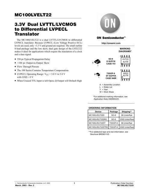
MC100LVELT22 3.3V Dual LVTTL/LVCMOS to Differential LVPECL ...
MC100LVELT22 3.3V Dual LVTTL/LVCMOS to Differential LVPECL ...
MC100LVELT22 3.3V Dual LVTTL/LVCMOS to Differential LVPECL ...

Create successful ePaper yourself
Turn your PDF publications into a flip-book with our unique Google optimized e-Paper software.
<strong>MC100LVELT22</strong><br />
<strong>3.3V</strong>Н<strong>Dual</strong> <strong>LVTTL</strong>/<strong>LVCMOS</strong><br />
<strong>to</strong> <strong>Differential</strong> <strong>LVPECL</strong><br />
Transla<strong>to</strong>r<br />
The <strong>MC100LVELT22</strong> is a dual <strong>LVTTL</strong>/<strong>LVCMOS</strong> <strong>to</strong> differential<br />
<strong>LVPECL</strong> transla<strong>to</strong>r. Because <strong>LVPECL</strong> (Low Voltage Positive ECL)<br />
levels are used, only +3.3 V and ground are required. The small outline<br />
8-lead package and the low skew, dual gate design of the LVELT22<br />
makes it ideal for applications which require the translation of a clock<br />
and a data signal.<br />
• 350 ps Typical Propagation Delay<br />
•
<strong>MC100LVELT22</strong><br />
Q0<br />
1<br />
8<br />
V CC<br />
Q0<br />
2<br />
7<br />
D0<br />
Q1<br />
3<br />
<strong>LVPECL</strong><br />
<strong>LVTTL</strong>/<br />
<strong>LVCMOS</strong><br />
6<br />
D1<br />
Q1<br />
4 5<br />
GND<br />
Figure 1. 8-Lead Pinout (Top View)<br />
and Logic Diagram<br />
PIN DESCRIPTION<br />
PIN<br />
FUNCTION<br />
Qn, Qn <strong>LVPECL</strong> <strong>Differential</strong> Outputs<br />
D0, D1 <strong>LVTTL</strong>/<strong>LVCMOS</strong> Inputs<br />
V CC Positive Supply<br />
GND Ground<br />
ATTRIBUTES<br />
Characteristics<br />
Internal Input Pulldown Resis<strong>to</strong>r<br />
Internal Input Pullup Resis<strong>to</strong>r<br />
ESD Protection<br />
Human Body Model<br />
Machine Model<br />
Value<br />
N/A<br />
N/A<br />
> 4 kV<br />
> 200 V<br />
Moisture Sensitivity, Indefinite Time Out of Drypack (Note 1) Level 1<br />
Flammability Rating Oxygen Index: 28 <strong>to</strong> 34 UL 94 V-0 @ 0.125 in<br />
Transis<strong>to</strong>r Count 164<br />
Meets or exceeds JEDEC Spec EIA/JESD78 IC Latchup Test<br />
1. For additional information, see Application Note AND8003/D.<br />
http://onsemi.com<br />
2
<strong>MC100LVELT22</strong><br />
MAXIMUM RATINGS (Note 2)<br />
Symbol Parameter Condition 1 Condition 2 Rating Units<br />
V CC Positive Power Supply GND = 0 V 7 V<br />
V I Input Voltage GND = 0 V V I V CC 7 V<br />
I out Output Current Continuous<br />
Surge<br />
TA Operating Temperature Range -40 <strong>to</strong> +85 °C<br />
T stg S<strong>to</strong>rage Temperature Range -65 <strong>to</strong> +150 °C<br />
JA Thermal Resistance (Junction-<strong>to</strong>-Ambient) 0 LFPM<br />
500 LFPM<br />
JC Thermal Resistance (Junction-<strong>to</strong>-Case) std bd SO-8 41 <strong>to</strong> 44 ± 5% °C/W<br />
JA Thermal Resistance (Junction-<strong>to</strong>-Ambient) 0 LFPM<br />
500 LFPM<br />
SO-8<br />
SO-8<br />
TSSOP-8<br />
TSSOP-8<br />
JC Thermal Resistance (Junction-<strong>to</strong>-Case) std bd TSSOP-8 41 <strong>to</strong> 44 ± 5% °C/W<br />
T sol Wave Solder
<strong>MC100LVELT22</strong><br />
Driver<br />
Device<br />
Q<br />
Q<br />
D<br />
D<br />
Receiver<br />
Device<br />
50 <br />
50 <br />
Figure 1. Typical Termination for Output Driver and Device Evaluation<br />
(See Application Note AND8020 - Termination of ECL Logic Devices.)<br />
V TT<br />
V TT = V CC - 2.0 V<br />
Resource Reference of Application Notes<br />
AN1404 - ECLinPS Circuit Performance at Non-Standard V IH Levels<br />
AN1405 - ECL Clock Distribution Techniques<br />
AN1406 - Designing with PECL (ECL at +5.0 V)<br />
AN1503 - ECLinPS I/O SPICE Modeling Kit<br />
AN1504 - Metastability and the ECLinPS Family<br />
AN1560 - Low Voltage ECLinPS SPICE Modeling Kit<br />
AN1568 - Interfacing Between LVDS and ECL<br />
AN1596 - ECLinPS Lite Transla<strong>to</strong>r ELT Family SPICE I/O Model Kit<br />
AN1650 - Using Wire-OR Ties in ECLinPS Designs<br />
AN1672 - The ECL Transla<strong>to</strong>r Guide<br />
AND8001 - Odd Number Counters Design<br />
AND8002 - Marking and Date Codes<br />
AND8020 - Termination of ECL Logic Devices<br />
AND8090 - AC Characteristics of ECL Devices<br />
http://onsemi.com<br />
4
<strong>MC100LVELT22</strong><br />
PACKAGE DIMENSIONS<br />
-X-<br />
-Y-<br />
B<br />
8<br />
1<br />
A<br />
5<br />
4<br />
S<br />
0.25 (0.010) M<br />
SO-8<br />
D SUFFIX<br />
PLASTIC SOIC PACKAGE<br />
CASE 751-07<br />
ISSUE AA<br />
Y<br />
M<br />
K<br />
NOTES:<br />
1. DIMENSIONING AND TOLERANCING PER ANSI<br />
Y14.5M, 1982.<br />
2. CONTROLLING DIMENSION: MILLIMETER.<br />
3. DIMENSION A AND B DO NOT INCLUDE MOLD<br />
PROTRUSION.<br />
4. MAXIMUM MOLD PROTRUSION 0.15 (0.006) PER<br />
SIDE.<br />
5. DIMENSION D DOES NOT INCLUDE DAMBAR<br />
PROTRUSION. ALLOWABLE DAMBAR<br />
PROTRUSION SHALL BE 0.127 (0.005) TOTAL IN<br />
EXCESS OF THE D DIMENSION AT MAXIMUM<br />
MATERIAL CONDITION.<br />
6. 751−01 THRU 751−06 ARE OBSOLETE. NEW<br />
STANDAARD IS 751−07<br />
-Z-<br />
H<br />
G<br />
D<br />
C<br />
0.25 (0.010) M Z Y S X S<br />
SEATING<br />
PLANE<br />
0.10 (0.004)<br />
N X 45<br />
M<br />
J<br />
MILLIMETERS INCHES<br />
DIM MIN MAX MIN MAX<br />
A 4.80 5.00 0.189 0.197<br />
B 3.80 4.00 0.150 0.157<br />
C 1.35 1.75 0.053 0.069<br />
D 0.33 0.51 0.013 0.020<br />
G 1.27 BSC 0.050 BSC<br />
H 0.10 0.25 0.004 0.010<br />
J 0.19 0.25 0.007 0.010<br />
K 0.40 1.27 0.016 0.050<br />
M 0 8 0 8 <br />
N 0.25 0.50 0.010 0.020<br />
S 5.80 6.20 0.228 0.244<br />
http://onsemi.com<br />
5
<strong>MC100LVELT22</strong><br />
PACKAGE DIMENSIONS<br />
TSSOP-8<br />
DT SUFFIX<br />
PLASTIC TSSOP PACKAGE<br />
CASE 948R-02<br />
ISSUE A<br />
0.15 (0.006) T<br />
0.15 (0.006) T<br />
L<br />
U<br />
U<br />
0.10 (0.004)<br />
SEATING<br />
PLANE<br />
S<br />
2X L/2<br />
PIN 1<br />
IDENT<br />
S<br />
C<br />
D<br />
8 5<br />
1<br />
8x<br />
K REF<br />
4<br />
0.10 (0.004) M T U S V S<br />
G<br />
DETAIL E<br />
DETAIL E<br />
F<br />
0.25 (0.010)<br />
M<br />
B<br />
-U-<br />
-T-<br />
A<br />
-V-<br />
-W-<br />
NOTES:<br />
1. DIMENSIONING AND TOLERANCING PER ANSI<br />
Y14.5M, 1982.<br />
2. CONTROLLING DIMENSION: MILLIMETER.<br />
3. DIMENSION A DOES NOT INCLUDE MOLD FLASH.<br />
PROTRUSIONS OR GATE BURRS. MOLD FLASH<br />
OR GATE BURRS SHALL NOT EXCEED 0.15<br />
(0.006) PER SIDE.<br />
4. DIMENSION B DOES NOT INCLUDE INTERLEAD<br />
FLASH OR PROTRUSION. INTERLEAD FLASH OR<br />
PROTRUSION SHALL NOT EXCEED 0.25 (0.010)<br />
PER SIDE.<br />
5. TERMINAL NUMBERS ARE SHOWN FOR<br />
REFERENCE ONLY.<br />
6. DIMENSION A AND B ARE TO BE DETERMINED<br />
AT DATUM PLANE −W−.<br />
MILLIMETERS INCHES<br />
DIM MIN MAX MIN MAX<br />
A 2.90 3.10 0.114 0.122<br />
B 2.90 3.10 0.114 0.122<br />
C 0.80 1.10 0.031 0.043<br />
D 0.05 0.15 0.002 0.006<br />
F 0.40 0.70 0.016 0.028<br />
G 0.65 BSC 0.026 BSC<br />
K 0.25 0.40 0.010 0.016<br />
L 4.90 BSC 0.193 BSC<br />
M 0 6 0 6 <br />
ON Semiconduc<strong>to</strong>r and are registered trademarks of Semiconduc<strong>to</strong>r Components Industries, LLC (SCILLC). SCILLC reserves the right <strong>to</strong> make<br />
changes without further notice <strong>to</strong> any products herein. SCILLC makes no warranty, representation or guarantee regarding the suitability of its products for any<br />
particular purpose, nor does SCILLC assume any liability arising out of the application or use of any product or circuit, and specifically disclaims any and all<br />
liability, including without limitation special, consequential or incidental damages. “Typical” parameters which may be provided in SCILLC data sheets and/or<br />
specifications can and do vary in different applications and actual performance may vary over time. All operating parameters, including “Typicals” must be<br />
validated for each cus<strong>to</strong>mer application by cus<strong>to</strong>mer’s technical experts. SCILLC does not convey any license under its patent rights nor the rights of others.<br />
SCILLC products are not designed, intended, or authorized for use as components in systems intended for surgical implant in<strong>to</strong> the body, or other applications<br />
intended <strong>to</strong> support or sustain life, or for any other application in which the failure of the SCILLC product could create a situation where personal injury or death<br />
may occur. Should Buyer purchase or use SCILLC products for any such unintended or unauthorized application, Buyer shall indemnify and hold SCILLC<br />
and its officers, employees, subsidiaries, affiliates, and distribu<strong>to</strong>rs harmless against all claims, costs, damages, and expenses, and reasonable at<strong>to</strong>rney fees<br />
arising out of, directly or indirectly, any claim of personal injury or death associated with such unintended or unauthorized use, even if such claim alleges that<br />
SCILLC was negligent regarding the design or manufacture of the part. SCILLC is an Equal Opportunity/Affirmative Action Employer.<br />
PUBLICATION ORDERING INFORMATION<br />
Literature Fulfillment:<br />
Literature Distribution Center for ON Semiconduc<strong>to</strong>r<br />
P.O. Box 5163, Denver, Colorado 80217 USA<br />
Phone: 303-675-2175 or 800-344-3860 Toll Free USA/Canada<br />
Fax: 303-675-2176 or 800-344-3867 Toll Free USA/Canada<br />
Email: ONlit@hibbertco.com<br />
N. American Technical Support: 800-282-9855 Toll Free USA/Canada<br />
JAPAN: ON Semiconduc<strong>to</strong>r, Japan Cus<strong>to</strong>mer Focus Center<br />
2-9-1 Kamimeguro, Meguro-ku, Tokyo, Japan 153-0051<br />
Phone: 81-3-5773-3850<br />
ON Semiconduc<strong>to</strong>r Website: http://onsemi.com<br />
For additional information, please contact your local<br />
Sales Representative.<br />
http://onsemi.com<br />
6<br />
<strong>MC100LVELT22</strong>/D