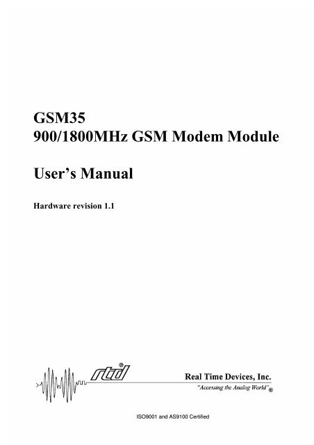
GSM35 900/1800MHz GSM Modem Module User's Manual
GSM35 900/1800MHz GSM Modem Module User's Manual
GSM35 900/1800MHz GSM Modem Module User's Manual

You also want an ePaper? Increase the reach of your titles
YUMPU automatically turns print PDFs into web optimized ePapers that Google loves.
<strong><strong>GSM</strong>35</strong><br />
<strong>900</strong>/<strong>1800MHz</strong> <strong>GSM</strong> <strong>Modem</strong> <strong>Module</strong><br />
User’s <strong>Manual</strong><br />
Hardware revision 1.1<br />
ISO<strong>900</strong>1 and AS9100 Certified
<strong><strong>GSM</strong>35</strong><br />
<strong>GSM</strong> <strong>Modem</strong> <strong>Module</strong><br />
User’s <strong>Manual</strong><br />
REAL TIME DEVICES FINLAND OY<br />
LEPOLANTIE 14<br />
FIN-00660 HELSINKI<br />
FINLAND<br />
Phone: (+358) 9 346 4538<br />
FAX: (+358) 9 346 4539<br />
EMail<br />
sales@rtdfinland.fi<br />
techsupport@rtdfinland.fi<br />
Websites<br />
http://www.rtdfinland.fi/<br />
http://www.rtdusa.com/<br />
User’s <strong>Manual</strong><br />
<strong><strong>GSM</strong>35</strong> 2 RTD Finland Oy
WARNING<br />
LIFE SUPPORT APPLICATIONS<br />
This product is not designed for use in life support appliances, devices or systems<br />
where malfunctioning of these products can reasonably be expected to result in<br />
personal injury. RTD customers using or selling this product for use in these<br />
applications do so at their own risk and fully agree to indemnify RTD for any<br />
damages resulting from such improper use or sale.<br />
SAFETY PRECAUTIONS FOR THE USER<br />
1) AIRCRAFT SAFETY<br />
The TC35 cellular engine used on the <strong><strong>GSM</strong>35</strong> can interfere with an aircraft’s<br />
navigation system and it’s cellular network. Using your <strong><strong>GSM</strong>35</strong> on board aircraft is<br />
forbidden by law. Failure to comply with this prohibition may lead to temporary<br />
suspension or permanent cancellation of cellular services for the person who<br />
infringes this prohibition and/or legal action against said person.<br />
2) ENVIRONMENTS WITH EXPLOSIVE SUBSTANCES<br />
Users are not advised to use the <strong><strong>GSM</strong>35</strong> in automotive service stations. Users are<br />
reminded of the necessity to comply with restrictions regarding the use of radio<br />
devices in fuel depots, chemical plants and locations where explosives are<br />
ignited.<br />
3) ELECTRONICS IN MEDICAL APPLICATIONS<br />
Radio transmitters such as the <strong><strong>GSM</strong>35</strong> can interfere with the operation of<br />
inadequately protected medical devices. Please address all questions to a doctor<br />
or manufacturer of the medical device.<br />
4) PRECAUTIONS IN THE EVENT OF LOSS/THEFT<br />
OF <strong><strong>GSM</strong>35</strong> AND SIM CARD<br />
If your <strong><strong>GSM</strong>35</strong>, SIM card or both go missing, notify your network operator<br />
immediately in order to avoid misuse.<br />
User’s <strong>Manual</strong><br />
<strong><strong>GSM</strong>35</strong> 3 RTD Finland Oy
Revision History<br />
05/04/2002 HW Release 1.0, Preliminary version, released<br />
CE Conformity of TC35 cellular engine:<br />
• 89/336/EC (EMC Directive)<br />
• 73/23/EC (Low voltage directive)<br />
• 91/263/EC (telecommunications terminals directive)<br />
Standards:<br />
• EMC ETS 300 342-1<br />
• Safety EN60950<br />
• <strong>GSM</strong> Network TBR 19, TBR 20<br />
Notice: We have attempted to verify all information in this manual as of<br />
the publication date. Information in this manual may change without prior<br />
notice from RTD Finland Oy.<br />
Published by:<br />
Real Time Devices Finland Oy<br />
Lepolantie 14<br />
FIN-00660 Helsinki<br />
Finland<br />
Copyright 2002 Real Time Devices Finland Oy<br />
All rights reserved<br />
Printed in Finland<br />
User’s <strong>Manual</strong><br />
PC/XT, PC/AT are registered trademarks of IBM Corporation.<br />
PC/104 is a registered trademark of the PC/104 Consortium.<br />
The Real Time Devices Logo is a registered trademark of Real Time Devices.<br />
utility<strong>Module</strong> is a trademark of Real Time Devices.<br />
All other trademarks appearing in this document are the property of their respective owners.<br />
<strong><strong>GSM</strong>35</strong> 4 RTD Finland Oy
Table of Contents<br />
List of illustrations and tables ................................6<br />
Chapter 1 Introduction ............................................7<br />
Features .................................................................................................. 7<br />
<strong>GSM</strong> cellular modem............................................................................... 7<br />
16C550 compatible UART....................................................................... 8<br />
I/O interfaces........................................................................................... 8<br />
Mechanical description............................................................................ 8<br />
Connector description ............................................................................. 8<br />
What comes with your board?................................................................. 9<br />
Using this manual.................................................................................... 9<br />
When you need help ............................................................................... 9<br />
Chapter 2 Board settings ...................................... 10<br />
Factory configured jumper settings ....................................................... 11<br />
Base address jumpers........................................................................... 12<br />
Host interrupts....................................................................................... 14<br />
Chapter 3 Board installation ................................. 15<br />
Board installation................................................................................... 15<br />
General purpose digital I/O connector .................................................. 16<br />
SIM card holder ..................................................................................... 17<br />
Chapter 4 Hardware description ........................... 19<br />
The <strong>GSM</strong> wireless modem module........................................................ 20<br />
<strong>GSM</strong> antenna considerations................................................................ 20<br />
SIM card reader .................................................................................... 21<br />
UART serial port circuitry ...................................................................... 21<br />
Digital I/O .............................................................................................. 22<br />
User’s <strong>Manual</strong><br />
<strong><strong>GSM</strong>35</strong> 5 RTD Finland Oy
Chapter 5 Board operation and programming..... 23<br />
Defining the memory map .................................................................... 23<br />
<strong>GSM</strong> BASE+400h Digital I/O................................................................. 24<br />
<strong>GSM</strong> BASE+402h status register .......................................................... 24<br />
<strong>GSM</strong> BASE+403h control register......................................................... 24<br />
Starting up and logging into the <strong>GSM</strong> network...................................... 25<br />
Interrupts ............................................................................................... 25<br />
Chapter 6 <strong><strong>GSM</strong>35</strong> Specifications .......................... 31<br />
Chapter 7 Return policy and warranty.................. 32<br />
List of illustrations and tables<br />
Fig. 2-1 <strong><strong>GSM</strong>35</strong> Board layout showing jumper locations<br />
Fig. 2-2 Base address jumpers illustrating address 2E8h<br />
Fig. 2-3 Interrupt jumpers from left to right: IRQ 2,5,6,7,10,11,12,15 and G<br />
Fig. 3-1 <strong><strong>GSM</strong>35</strong> integrated in a RTD PC/104 cpu<strong>Module</strong> stack<br />
together with a HPWR104HR and a CMM series cpu<strong>Module</strong><br />
Fig. 3-2 Digital I/O connector layout of the <strong><strong>GSM</strong>35</strong><br />
Fig. 3-3 External SIM card interface of the <strong><strong>GSM</strong>35</strong><br />
Fig. 3-4 ESIM2035 External SIM card interface board<br />
Fig. 3-5 External SIM card header J25 (Only on <strong><strong>GSM</strong>35</strong>-2 boards)<br />
Fig. 4-1 Block diagram of the <strong><strong>GSM</strong>35</strong><br />
Table 2-1 Factory configured jumper settings<br />
Table 2-2 Base address jumper settings <strong><strong>GSM</strong>35</strong><br />
Table 3-1 Pin outs of the <strong><strong>GSM</strong>35</strong> digital I/O interface connector<br />
Table 5-1 General I/O map of the <strong><strong>GSM</strong>35</strong> UART<br />
User’s <strong>Manual</strong><br />
<strong><strong>GSM</strong>35</strong> 6 RTD Finland Oy
Chapter 1 - INTRODUCTION<br />
This user’s manual describes the operation of the RTD <strong><strong>GSM</strong>35</strong> integrated<br />
global <strong>GSM</strong> wireless modem designed for mobile, marine, and automotive<br />
applications.<br />
Features<br />
Some of the key features of the <strong><strong>GSM</strong>35</strong> include:<br />
• Low power Dual band Siemens TC35 cellular engine, <strong>GSM</strong><strong>900</strong>/1800Mhz<br />
• 9,6/14,4 kbit/s datarate, group 3 faxes, SMS and SMS cell broadcast<br />
• Onboard SIM-card socket for 3V standard cards<br />
• 16C550 UART interfaces to host computer<br />
• Supports COM1,COM2,COM3,COM4 or COMx<br />
• Available IRQ’s 2,5,6,7,10,11,12,14,15<br />
• Status LED indicating <strong>GSM</strong> activity and status<br />
• 16 TTL I/O’s 8 outputs 8 inputs<br />
• +5V only operation, 2.3W typical<br />
• Wide operating temperature range –20 to + 70C guaranteed<br />
• Onboard temperature sensor<br />
• Fully PC/104 compliant, IDAN versions available<br />
The following paragraphs briefly describe the major features of the <strong><strong>GSM</strong>35</strong>. A<br />
more detailed discussion is included in Chapter 4 (Hardware description) The<br />
boards installation is described in Chapter 2 (Board Installation).<br />
<strong>GSM</strong> cellular modem<br />
The Real Time Devices <strong><strong>GSM</strong>35</strong> wireless <strong>GSM</strong> modem unit provides a<br />
direct and reliable <strong>GSM</strong> connection to stationary or <strong>GSM</strong> <strong>900</strong>/1800 mobile<br />
fields around the world. <strong>GSM</strong> connectivity is achieved using the Siemens<br />
TC35 engine. This unit works in the <strong>900</strong>/<strong>1800MHz</strong> band supporting <strong>GSM</strong><br />
02.22 network and service provider personalisation.<br />
Connect any standard <strong>GSM</strong> antenna directly to the OSX connector of the<br />
<strong><strong>GSM</strong>35</strong>. The antenna should be connected to the TC35 using a flexible<br />
50-Ohm antenna cable. In IDAN installations the antenna connection is<br />
brought to the front side of the IDAN-frame. The antenna used should<br />
meet the following specifications: Frequency 890-910MHz (TX), 935-<br />
960MHz (RX); Impedance 50 Ohms; VSWR 1,7:1 (TX) 1,9:1 (RX); Gain<br />
A SIM-card socket is located on the solder side of the module. The card<br />
can only be removed while the TC35 has been placed in shutdown mode.<br />
The GPRS35 is also available using the MC35 GPRS <strong>Modem</strong>. It supports<br />
all the features of the <strong><strong>GSM</strong>35</strong> and, on top, the advantages of the fast<br />
GPRS technology. The MC35 based GPRS modem GPRS35 is available<br />
now. During the 3Q 2002 RTD Finland will also release a triple band<br />
GPRS module that will operate in the 1<strong>900</strong>MHz band. The part number<br />
will be GPRS45. Engineering samples will be available in August 2002.<br />
16C550 compatible UART<br />
Communication to the <strong><strong>GSM</strong>35</strong> board is performed through a standard<br />
UART channel. This onboard serial port leaves the other system serial<br />
ports free for the user. All operating systems will recognize and support<br />
this 16C550 standard UART, and therefore no special communication<br />
drivers are needed to receive data from your <strong><strong>GSM</strong>35</strong> board. The address<br />
and interrupt of your serial channels can be individually set with the<br />
onboard jumper fields.<br />
I/O interfaces<br />
The <strong><strong>GSM</strong>35</strong> can be controlled and monitored from the software through<br />
two dedicated I/O registers. A special I/O connector is available for the<br />
user to connect to the general-purpose TTL level digital I/O.<br />
Mechanical description<br />
The <strong><strong>GSM</strong>35</strong> is designed on a PC/104 form factor. An easy mechanical<br />
interface to both PC/104 and RTD IDAN systems can be achieved. Stack<br />
your <strong><strong>GSM</strong>35</strong> directly on a PC/104 compatible CPU module using the<br />
onboard mounting holes and standoffs.<br />
Connector description<br />
The GPS and <strong>GSM</strong> antenna interfaces use an OSX type miniature coaxial<br />
connector. Connect your antenna directly to the <strong><strong>GSM</strong>35</strong> antenna<br />
connectors, or use a short cable inside your enclosure to connect to a<br />
feed through connector to allow connection of the antennas to the wall of<br />
your enclosure. All I/O connections are made using header type terminals.<br />
User’s <strong>Manual</strong><br />
<strong><strong>GSM</strong>35</strong> 8 RTD Finland Oy
What comes with your board<br />
Your <strong><strong>GSM</strong>35</strong> package contains the following items:<br />
• <strong><strong>GSM</strong>35</strong> board<br />
• <strong>User's</strong> manual<br />
Note: Device drivers and example software available on our website<br />
If any item is missing or damaged, please send an EMAIL to Real Time<br />
Devices Finland sales service department at Internet address:<br />
.<br />
Note that RTD Finland also can offer a <strong><strong>GSM</strong>35</strong> starter kit that will include<br />
an active antenna with ready cables for direct evaluation and testing of<br />
this module. The part number for this starter kit is SK-<strong><strong>GSM</strong>35</strong>.<br />
Using this manual<br />
This manual is intended to help you install your new <strong><strong>GSM</strong>35</strong> module and<br />
get it working quickly, while also providing enough detail about the board<br />
and it's functions so that you can enjoy maximum use of it's features even<br />
in the most demanding applications.<br />
When you need help<br />
This manual and all the example programs will provide you with enough<br />
information to fully utilize all the features on this board. If you have any<br />
problems installing or using this board, contact our Technical support<br />
department at . When sending us an Email<br />
request please include the following information: Your company's name<br />
and address, your name, your telephone number, and a brief description<br />
of the problem.<br />
User’s <strong>Manual</strong><br />
<strong><strong>GSM</strong>35</strong> 9 RTD Finland Oy
Chapter 2 - BOARD SETTINGS<br />
The <strong><strong>GSM</strong>35</strong> board has jumper settings, which can be changed to suit your<br />
application and host computer configuration. The factory settings are<br />
listed and shown in the diagram at the beginning of this chapter. Make<br />
sure you completely study and understand this chapter before making<br />
changes to these settings.<br />
User’s <strong>Manual</strong><br />
<strong><strong>GSM</strong>35</strong> 10 RTD Finland Oy
Factory-Configured Jumper Settings<br />
Table 2-1 below illustrates the factory jumper setting for the <strong><strong>GSM</strong>35</strong>.<br />
Figure 2-1 shows the board layout of the <strong><strong>GSM</strong>35</strong> and the locations of the<br />
jumpers. The following paragraphs explain how to change the factory<br />
jumper settings to suit your specific application.<br />
Table 2-1 Factory configured jumper settings (Please see figure 2-1 below<br />
for more detailed locations)<br />
User’s <strong>Manual</strong><br />
JUMPER NAME DESCRIPTION NUMBER OF JUMPERS FACTORY SETTING<br />
BASE Base Addresses 6 2E8 / 6E8<br />
IRQ Host interrupts 11+1 5, G – jumper closed<br />
Fig. 2-1 <strong><strong>GSM</strong>35</strong>-1 Board layout showing jumper locations<br />
<strong><strong>GSM</strong>35</strong> 11 RTD Finland Oy
Base address jumpers (Factory setting: 2E8h / 6E8h)<br />
The <strong><strong>GSM</strong>35</strong> is I/O mapped into the memory space of your host XT/AT.<br />
The board occupies a consecutive memory window of 8 bytes starting<br />
from the base address for UART communication and 4 consecutive bytes<br />
starting from BASE+400h for the board control and status registers. As an<br />
example if your base address is set to be 2E8h for the serial port, the<br />
onboard control registers will start from 6E8h.<br />
The most common cause of failure when you are first setting up your<br />
module is address contention: some of your computers I/O space is<br />
already occupied by other devices and memory resident programs. When<br />
the <strong><strong>GSM</strong>35</strong> attempts to use it's own reserved memory addresses (which<br />
are being already used by another peripheral device) erratic performance<br />
can occur and the data read from the board may be corrupted.<br />
To avoid this problem make sure you set up the base address by using<br />
the six jumpers on the right side of the board, this allows you to choose<br />
from a number of different addresses in your host computer’s I/O map.<br />
Should the factory-installed settings be incompatible to your system<br />
configuration, you may change this setting to another using the options<br />
illustrated in Table 2-2 (overleaf). The table shows the jumper settings<br />
and their corresponding values in hexadecimal form. Ensure that you<br />
verify the correct location of the base address jumpers. When the jumper<br />
is removed it corresponds to a logical "0", connecting the jumper to a "1".<br />
When you set the base address of the module, record the setting inside<br />
the back cover of this manual.<br />
User’s <strong>Manual</strong><br />
<strong><strong>GSM</strong>35</strong> 12 RTD Finland Oy
<strong><strong>GSM</strong>35</strong> Base address configuration<br />
BASE A8 A7 A6 A5 A4 A3 BASE A8 A7 A6 A5 A4 A3<br />
200 0 0 0 0 0 0 300 1 0 0 0 0 0<br />
208 0 0 0 0 0 1 308 1 0 0 0 0 1<br />
210 0 0 0 0 1 0 310 1 0 0 0 1 0<br />
218 0 0 0 0 1 1 318 1 0 0 0 1 1<br />
220 0 0 0 1 0 0 320 1 0 0 1 0 0<br />
228 0 0 0 1 0 1 328 1 0 0 1 0 1<br />
230 0 0 0 1 1 0 330 1 0 0 1 1 0<br />
238 0 0 0 1 1 1 338 1 0 0 1 1 1<br />
240 0 0 1 0 0 0 340 1 0 1 0 0 0<br />
248 0 0 1 0 0 1 348 1 0 1 0 0 1<br />
250 0 0 1 0 1 0 350 1 0 1 0 1 0<br />
258 0 0 1 0 1 1 358 1 0 1 0 1 1<br />
260 0 0 1 1 0 0 360 1 0 1 1 0 0<br />
268 0 0 1 1 0 1 368 1 0 1 1 0 1<br />
270 0 0 1 1 1 0 370 1 0 1 1 1 0<br />
278 0 0 1 1 1 1 378 1 0 1 1 1 1<br />
280 0 1 0 0 0 0 380 1 1 0 0 0 0<br />
288 0 1 0 0 0 1 388 1 1 0 0 0 1<br />
290 0 1 0 0 1 0 390 1 1 0 0 1 0<br />
298 0 1 0 0 1 1 398 1 1 0 0 1 1<br />
2A0 0 1 0 1 0 0 3A0 1 1 0 1 0 0<br />
2A8 0 1 0 1 0 1 3A8 1 1 0 1 0 1<br />
2B0 0 1 0 1 1 0 3B0 1 1 0 1 1 0<br />
2B8 0 1 0 1 1 1 3B8 1 1 0 1 1 1<br />
2C0 0 1 1 0 0 0 3C0 1 1 1 0 0 0<br />
2C8 0 1 1 0 0 1 3C8 1 1 1 0 0 1<br />
2D0 0 1 1 0 1 0 3D0 1 1 1 0 1 0<br />
2D8 0 1 1 0 1 1 3D8 1 1 1 0 1 1<br />
2E0 0 1 1 1 0 0 3E0 1 1 1 1 0 0<br />
2E8 0 1 1 1 0 1 3E8 1 1 1 1 0 1<br />
2F0 0 1 1 1 1 0 3F0 1 1 1 1 1 0<br />
2F8 0 1 1 1 1 1 3F8 1 1 1 1 1 1<br />
0 = JUMPER OFF 1 = JUMPER CLOSED<br />
Table 2-2 Base address jumper settings for the <strong><strong>GSM</strong>35</strong>, the default jumper<br />
setting is highlighted.<br />
User’s <strong>Manual</strong><br />
<strong><strong>GSM</strong>35</strong> 13 RTD Finland Oy
Fig. 2-2 Base address jumpers illustrating address 2E8<br />
Host interrupts (Factory setting: IRQ5, G closed)<br />
The header connector, shown in Figure 2-3 below, lets you connect the<br />
onboard control logic interrupt outputs to one of the interrupt channels<br />
available on the host computer XT/AT bus.<br />
User’s <strong>Manual</strong><br />
Fig. 2-3 Interrupt jumpers from left to right IRQ2,5,6,7,10,11,12,14,15 and G<br />
Note: The <strong><strong>GSM</strong>35</strong> hardware supports interrupt sharing! Jumper G must be<br />
closed on one module per used interrupt. For example if two boards share<br />
interrupt number 7 only one board may have the G jumper closed. The G<br />
jumper connects a 1KOhm resistor to ground while the shared interrupts<br />
are 3-stated pulling the line to an inactive level.<br />
<strong><strong>GSM</strong>35</strong> 14 RTD Finland Oy
Chapter 3 BOARD INSTALLATION<br />
The <strong><strong>GSM</strong>35</strong> <strong>GSM</strong> modem module is designed to directly mount on top or<br />
under your RTD PC/104 cpu<strong>Module</strong> stack. This chapter tells you step-bystep<br />
how to install your <strong><strong>GSM</strong>35</strong> into your system.<br />
Board installation<br />
Keep your board in its antistatic bag until you are ready to install it to your<br />
system! When removing it from the bag, hold the board at the edges and<br />
do not touch the components or connectors. Please handle the board in<br />
an antistatic environment and use a grounded workbench for testing and<br />
handling of your hardware. Before installing the board in your computer,<br />
check the power cabling. Failure to do so may cause the power supply<br />
unit to malfunction or even cause permanent damage.<br />
General installation guidelines:<br />
• Touch the grounded metal housing of your computer to discharge any<br />
antistatic buildup and then remove the board from its antistatic bag.<br />
• Hold the board by the edges and install it in an enclosure or place it on<br />
the table on an antistatic surface<br />
• Install your board in your system, and wire the power supply correctly.<br />
Failure to do so may cause the power supply unit to malfunction or<br />
even cause permanent damage to the device.<br />
• Check all wiring connections once and then once more again<br />
• Connect the SIM card and the <strong>GSM</strong> antenna to the OSX connector on<br />
the <strong><strong>GSM</strong>35</strong> board<br />
• Apply power to your system<br />
User’s <strong>Manual</strong><br />
<strong><strong>GSM</strong>35</strong> 15 RTD Finland Oy
Fig. 3-1 <strong><strong>GSM</strong>35</strong> integrated in a RTD PC/104 cpu<strong>Module</strong> stack together<br />
with a HPWR104HR power supply module and a CMM series cpu<strong>Module</strong><br />
General purpose digital I/O connector<br />
The Table 3-1 below shows the pin outs of the <strong><strong>GSM</strong>35</strong> digital I/O<br />
interface. The signals in this geader connector can be used as general<br />
purpose TTL level I/O lines to interface to LCD displays, LED’s, bush<br />
buttons or relays. Note that Figure 3-2 shows two connectors together.<br />
The connector J28 carries all inputs and J3 carries all the outputs.<br />
PIN J2 Description PIN J2 Description<br />
1 GND 2 Out0<br />
3 Out1 4 Out2<br />
5 Out3 6 Out4<br />
7 Out5 8 Out6<br />
9 Out7 10 +5V<br />
PIN J16 Description PIN J16 Description<br />
1 GND 2 In0<br />
3 In1 4 In2<br />
5 In3 6 In4<br />
7 In5 8 In6<br />
9 In7 10 +5V<br />
Table 3-1 Pin outs of the <strong><strong>GSM</strong>35</strong> digital I/O interface connector<br />
User’s <strong>Manual</strong><br />
<strong><strong>GSM</strong>35</strong> 16 RTD Finland Oy
Fig 3-2 Digital I/O connector layout of the <strong><strong>GSM</strong>35</strong><br />
SIM card holder<br />
The figure 3-3 below shows the mechanical construction of the +3V<br />
standard SIM-card holder. In the figure the card is in the ejected state.<br />
Press the card carrier into the holder. To eject the SIM-card, press the<br />
yellow ejector button. The <strong><strong>GSM</strong>35</strong> also supports an external SIM card<br />
interface board the ESIM2035. This external card interface can be<br />
attached to the wall of your enclosure with a 150mm long cable. This is<br />
the maximum guaranteed length.<br />
Fig 3-3 External SIM card interface of the <strong><strong>GSM</strong>35</strong>.<br />
User’s <strong>Manual</strong><br />
<strong><strong>GSM</strong>35</strong> 17 RTD Finland Oy
Figure 3-4 below shows a picture of the external SIM card interface board.<br />
Fig 3-4 ESIM2035 board<br />
Note that the ESIM2035 is configured differently for the <strong>GSM</strong>20 and the<br />
<strong><strong>GSM</strong>35</strong>/GPRS35. The units are not interchangeable, the <strong><strong>GSM</strong>35</strong> and the<br />
GPRS are identical in their SIM interfaces. Once the TC35 <strong>GSM</strong> modem<br />
is able to initialise itself after power-up and correctly detect the SIM card<br />
the green status LED will be lit. If the LED is not illuminated you can not<br />
interface to your <strong>GSM</strong> modem. See Figure 3-3 for the location of the<br />
“STAT” LED. The header/mounting holes immediately next to the LED can<br />
be used to connect to an LED externally mounted to the enclosure wall for<br />
example. The “STAT” LED will not indicate detection of the <strong>GSM</strong> field or<br />
network access.<br />
External SIM card interface J25<br />
The figure 3-4 below shows the <strong><strong>GSM</strong>35</strong> external SIM card interface<br />
header J25 that is used to connect to board the ESIM2035.<br />
Fig 3-5 External SIM card header J25 available only on <strong><strong>GSM</strong>35</strong>-2 boards<br />
User’s <strong>Manual</strong><br />
<strong><strong>GSM</strong>35</strong> 18 RTD Finland Oy
Chapter 4 - HARDWARE DESCRIPTION<br />
This chapter describes the major hardware building blocks of the <strong><strong>GSM</strong>35</strong>:<br />
• The <strong>GSM</strong> wireless modem module<br />
• <strong>GSM</strong> antenna considerations<br />
• SIM card reader<br />
• UART serial port circuitry<br />
• Digital I/O<br />
Fig. 4-1 Block diagram of the <strong><strong>GSM</strong>35</strong><br />
User’s <strong>Manual</strong><br />
<strong><strong>GSM</strong>35</strong> 19 RTD Finland Oy
The <strong>GSM</strong> wireless modem module<br />
The <strong><strong>GSM</strong>35</strong> wireless <strong>GSM</strong> modem is built around the Siemens TC35 dual<br />
band <strong>900</strong>/<strong>1800MHz</strong> cellular engine. It is designed both for handling<br />
complex industrial applications such as telemetry, telematics or<br />
communication, and for integration in stationary or mobile fields all over<br />
the world. General information on these products is available at the<br />
following Internet addresses: http://www.siemens.de/gsm_e and<br />
http://www.siemens.de/gsm in german language.<br />
The <strong><strong>GSM</strong>35</strong> is capable of powerful communication over a speed of 9,6<br />
kbps or CSD up to 14,4 kbps (as of 06/2001). It is capable of FAX and<br />
SMS text messages. The data terminal rate is 9600 baud for all host<br />
commands (AT commands). The <strong><strong>GSM</strong>35</strong> modem module antenna<br />
interface connector uses an OSX connector. The mating antenna<br />
connectors and cables are supplied from RTD Finland Oy. Temperature<br />
monitoring is possible using the onboard temperature sensor. Limit data<br />
can be interrogated from the <strong><strong>GSM</strong>35</strong> status register bits 2-3.<br />
<strong>GSM</strong> Antenna considerations<br />
The antenna used must meet the following specifications: Frequency 890-<br />
910 MHz (TX), 935-960MHz (RX); Impedance 50 Ohms; VSWR 1,7:1 (TX)<br />
1,9:1 (RX); Gain 11) shows<br />
the quality of the network signal.<br />
User’s <strong>Manual</strong><br />
<strong><strong>GSM</strong>35</strong> 20 RTD Finland Oy
SIM-card reader<br />
Standard 3V and dual voltage SIM-cards can be used with the <strong><strong>GSM</strong>35</strong>.<br />
Older 5V SIM cards will not work, though they may operate in standard<br />
<strong>GSM</strong> cellular phones. These new 3V SIM cards are no older than two<br />
years. The SIM-card holder has a card detection circuit that will in theory<br />
allow hot insertion and removal of the card. This is NOT recommended,<br />
since the SIM card contenets can become corrupted if it is removed while<br />
the TC35 <strong>GSM</strong> modem is writing to it.<br />
A very useful AT command that shows detestion of the SIM card is:<br />
AT^SCID. The SIM card identifier is given as a reply ^SCID: value shows<br />
the ID of the SIM card. If no ID is detected the TC35 can not read the SIM<br />
card and can not connect to the <strong>GSM</strong> service provider network.<br />
To add an entry to your SIM card you may use the AT+CPBW command.<br />
In this example we add the RTD Finland phone number +358 9 346 4538<br />
to the SIM card memory location “1” with the following AT command set:<br />
AT+CPBW=1,35893464538,145,RTDFinland<br />
AT+CREG? Will indicate if the <strong><strong>GSM</strong>35</strong> is logged into the network. If the<br />
reply for example is +CREG: 0,1 it means that connection to the home<br />
network is valid. A complete AT-instruction set documentation is included<br />
in the TC35 user’s manual.<br />
UART serial port circuitry<br />
<strong>GSM</strong> data is sent and received through a standard 16C550 compatible<br />
UART. All today’s operating systems will recognize and support this serial<br />
communication device. The <strong><strong>GSM</strong>35</strong> uses its own onboard serial port and<br />
will not reserve serial port resources from the system. The I/O base<br />
address and interrupt for this serial port can be flexibly set as has been<br />
described in previous chapters of this manual. This user’s manual will not<br />
wade into details of serial port programming. This information is<br />
commonly available today. You can use any communication software<br />
package or terminal program to connect to your <strong><strong>GSM</strong>35</strong> UART. Just make<br />
sure you set up the I/O and IRQ are set right. The correct terminal speed<br />
for AT commands is 9600 baud, 8 databits, no parity, one stopbit, and<br />
hardware handshake. The UART on the board is specified for full<br />
operation from –40 to +85C. The oscillator frequency is set to be<br />
1.8432MHz. Note that the UART interrupt can be disabled or enabled<br />
from software by writing to bit 01 in address BASE+0x402.<br />
User’s <strong>Manual</strong><br />
<strong><strong>GSM</strong>35</strong> 21 RTD Finland Oy
Digital I/O<br />
For general-purpose digital I/O interfacing a 16-bit digital I/O port is<br />
provided. This port includes 8 TTL-level digital outputs that are cleared (to<br />
0) after system reset. Also are included 8 digital inputs with 10K Ohm pulldown<br />
resistors. These I/O’s are located on the left side of the board.<br />
These I/O’s are ideal to be used to interface to LCD displays, LED’s<br />
pushbuttons or other low power controls.<br />
User’s <strong>Manual</strong><br />
<strong><strong>GSM</strong>35</strong> 22 RTD Finland Oy
Chapter 5 BOARD OPERATION AND PROGRAMMING<br />
This chapter shows you how to program and use your <strong><strong>GSM</strong>35</strong>. It provides<br />
a general description of the I/O map. Detailed serial port programming tips<br />
are not within the scope of this manual.<br />
Defining the Memory Map<br />
The memory map of the <strong><strong>GSM</strong>35</strong> occupies two groups of eight bytes of<br />
host PC I/O space. This window is freely selectable by the user as<br />
described in Chapter 2, Table 2-2. After setting the base address you<br />
have access to the internal resources of the <strong><strong>GSM</strong>35</strong> control logic. These<br />
resources are not described in detail, since they are mapped as a<br />
standard PC serial port. For more details on the EXAR ST16C550IJ44<br />
UART chip programming please download the component specific data t<br />
from the website: http://www.exar.com/products/st16c550.html<br />
ADDR (hex) REGISTER DIR COMMENTS<br />
BASE<br />
BASE+1<br />
TXD O Only if control reg. Bit 7=0<br />
RXD I Only if control reg. Bit 7=0<br />
BAUD div. Low Only if control reg. Bit 7=1<br />
BAUD div. High Only if control reg. Bit 7=1<br />
IRQ enable Only if control reg. Bit 7=0<br />
BASE+2 IRQ ID<br />
BASE+3 Line control<br />
BASE+4 <strong>Modem</strong> control<br />
BASE+5 Line status<br />
BASE+6 <strong>Modem</strong> status<br />
BASE+400 Digital I/O I/O Digital I/O port<br />
BASE+402 <strong>GSM</strong> status I/O Configuration registers<br />
BASE+403 <strong>GSM</strong> control I/O Power control<br />
Table 5-1a General I/O map of the <strong><strong>GSM</strong>35</strong> UART<br />
User’s <strong>Manual</strong><br />
<strong><strong>GSM</strong>35</strong> 23 RTD Finland Oy
BASE+400 Digital I/O (R/W)<br />
This address is used to interface to the digital I/O port of the<br />
<strong><strong>GSM</strong>35</strong>, writing to this address will transfer the data out of the output port,<br />
while reading from this address will return the data from the digital inputs.<br />
BASE+402 <strong>GSM</strong> Status (R/W, 0x00 after reset)<br />
Write<br />
Bit 0 RESERVED<br />
Bit 1 /EN_INT 0 – UART interrupt enabled; 1 - disabled<br />
Bit 2 RESERVED<br />
Bit 3 RESERVED<br />
Read<br />
Bit 0 /EN_RST state<br />
Bit 1 /EN_INT state<br />
Bit 2 TEMP_LOW 1 - Board temperature below –20C<br />
Bit 3 TEMP_HIGH 1 - Board temperature over +70C<br />
BASE+403 <strong>GSM</strong> Control (R/W, 0x00 after reset)<br />
Write<br />
Bit 0 Ignition signal 1 – > 0 – results in IGN signal<br />
Bit 1 Powerdown of the TC35 1 – Power down; 0 – Power on<br />
Bit 2 RESERVED<br />
Bit 3 RESERVED<br />
Read<br />
Bit 0 Ignition signal state<br />
Bit 1 Powerdown of the TC35 state<br />
Bit 2 RESERVED<br />
Bit 3 RESERVED<br />
User’s <strong>Manual</strong><br />
<strong><strong>GSM</strong>35</strong> 24 RTD Finland Oy
Starting up and logging into the <strong>GSM</strong> network<br />
With no power applied insert your +3V or dual voltage SIM into the cardholder<br />
on the solder side of the board. Connect the antenna cable to the<br />
TC35 antenna connector and power up your PC/104 system. The <strong><strong>GSM</strong>35</strong><br />
will initioalise with the system. After this the status LED will blink for a<br />
while until the TC35 is logged into the network. If you have the PIN code<br />
enabled, the <strong><strong>GSM</strong>35</strong> status LED will continue to blink until the PIN code is<br />
given through the terminal mode with AT command AT+CPIN”XXXX”,<br />
unless AT^SFLC (facility lock for PIN code) has been set. Once the<br />
<strong><strong>GSM</strong>35</strong> is logged onto the network the LED will be lit continuously.<br />
INTERRUPTS<br />
What is an interrupt?<br />
An interrupt is an event that causes the processor in your computer to<br />
temporarily halt its current process and execute another routine. Upon<br />
completion of the new routine, control is returned to the original routine at<br />
the point where its execution was interrupted.<br />
Interrupts are a very flexible way of dealing with asynchronous events.<br />
Keyboard activity is a good example; your computer cannot predict when<br />
you might press a key and it would be a waste of processor time to do<br />
nothing whilst waiting for a keystroke to occur. Thus the interrupt scheme<br />
is used and the processor proceeds with other tasks. When a keystroke<br />
finally occurs, the keyboard then 'interrupts' the processor so that it can<br />
get the keyboard data. It then places it into the memory, and then returns<br />
to what it was doing before the interrupt occurred. Other common devices<br />
that use interrupts are A/D boards, network boards, other used serial<br />
ports etc.<br />
Interrupt request lines<br />
To allow different peripheral devices to generate interrupts on the same<br />
computer, the PC AT bus has interrupt request channels (IRQ's). A rising<br />
edge transition on one of these lines will be latched into the interrupt<br />
controller. The interrupt controller checks to see if the interrupts are to be<br />
acknowledged from that IRQ and, if another interrupt is being processed,<br />
it decides if the new request should supercede the one in progress or if it<br />
has to wait until the one in progress has been completed. The priority<br />
level of the interrupt is determined by the number of the IRQ as follows;<br />
IRQ0 has the highest priority whilst IRQ15 has the lowest. Many of the<br />
IRQ's are already used by the standard system resources, IRQ0 is<br />
dedicated to the internal timer, IRQ1 is dedicated to the keyboard input,<br />
User’s <strong>Manual</strong><br />
<strong><strong>GSM</strong>35</strong> 25 RTD Finland Oy
IRQ3 for the serial port COM2, and IRQ4 for the serial port COM1. Often<br />
interrupts 2,5,7,10,11 and 15 are free for the user.<br />
8259 Programmable Interrupt Controller<br />
The chip responsible for handling interrupt requests in a PC is the 8259<br />
Interrupt Controller. To use interrupts you will need to know how to read<br />
and set the 8259's internal interrupt mask register (IMR) and how to send<br />
the end-of-interrupt (EOI) command to acknowledge the 8259 interrupt<br />
controller.<br />
Interrupt Mask Register (IMR)<br />
Each bit in the interrupt mask register (IMR) contains the mask status of<br />
the interrupt line. If a bit is set (equal to 1), then the corresponding IRQ is<br />
masked, and it will not generate an interrupt. If a bit is cleared (equal to<br />
0), then the corresponding IRQ is not masked, and it can then generate<br />
an interrupt. The interrupt mask register is programmed through port 21h.<br />
End-of-Interrupt (EOI) Command<br />
After an interrupt service routine is complete, the 8259 Interrupt Controller<br />
must be acknowledged by writing the value 20h to port 20h.<br />
What exactly happens when an interrupt occurs?<br />
Understanding the sequence of events when an interrupt is triggered is<br />
necessary to correctly write interrupt handlers. When an interrupt request<br />
line is driven high by a peripheral device (such as the <strong><strong>GSM</strong>35</strong>), the<br />
interrupt controller checks to see if interrupts are enabled for that IRQ. It<br />
then checks to see if other interrupts are active or requested and<br />
determines which interrupt has priority. The interrupt controller then<br />
interrupts the processor. The current code segment (CS), instruction<br />
pointer (IP), and flags are pushed onto the system stack, and a new set if<br />
CS and IP are loaded from the lowest 1024 bytes of memory.<br />
This table is referred to as the interrupt vector table and each entry to this<br />
table is called an interrupt vector. Once the new CS and IP are loaded<br />
from the interrupt vector table, the processor starts to execute code from<br />
the new Code Segment (CS) and from the new Instruction Pointer (IP).<br />
When the interrupt routine is completed, the old CS and IP are popped<br />
from the system stack and the program execution continues from the point<br />
where interruption occurred.<br />
User’s <strong>Manual</strong><br />
<strong><strong>GSM</strong>35</strong> 26 RTD Finland Oy
Using Interrupts in your Program<br />
Adding interrupt support to your program is not as difficult as it may seem<br />
especially when programming under DOS. The following discussion will<br />
cover programming under DOS. Note that even the smallest mistake in<br />
your interrupt program may cause the computer to hang up and will only<br />
restart after a reboot. This can be frustrating and time-consuming.<br />
Writing an Interrupt Service Routine (ISR)<br />
The first step in adding interrupts to your software is to write an interrupt<br />
service routine (ISR). This is the routine that will be executed<br />
automatically each time an interrupt request occurs for the specified IRQ.<br />
An ISR is different from other sub-routines or procedures. First on<br />
entrance the processor registers must be pushed onto the stack before<br />
anything else! Second, just before exiting the routine, you must clear the<br />
interrupt on the <strong><strong>GSM</strong>35</strong> by writing to the Status register, and write the EOI<br />
command to the interrupt controller. Finally, when exiting the interrupt<br />
routine the processor registers must be popped from the system stack and<br />
you must execute the IRET assembly instruction. This instruction pops the<br />
CS, IP and processor flags from the system stack. These were pushed<br />
onto the stack when entering the ISR.<br />
Most compilers allow you to identify a function as an interrupt type and will<br />
automatically add these instructions to your ISR with one exception: most<br />
compilers do not automatically add the EOI command to the function, you<br />
must do it yourself. Other than this and a few exceptions discussed below,<br />
you can write your ISR as any code routine. It can call other functions and<br />
procedures in your program and it can access global data. If you are<br />
writing your first ISR, we recommend you stick to the basics; just<br />
something that enables you to verify you have entered the ISR and<br />
executed it successfully. For example: set a flag in your ISR and in your<br />
main program check for the flag.<br />
Note: If you choose to write your ISR in in-line Assembly, you must push<br />
and pop registers correctly and exit the routine with the IRET<br />
instruction instead of the RET instruction.<br />
User’s <strong>Manual</strong><br />
There are a few precautions you must consider when writing ISR's. The<br />
most important is, do not use any DOS functions or functions that call<br />
DOS functions from an interrupt routine. DOS is not re-entrant; that is, a<br />
DOS function cannot call itself. In typical programming, this will not happen<br />
because of the way DOS is written. But what about using interrupts?<br />
Consider then the following situation in your program: If DOS function X is<br />
being executed when an interrupt occurs and the interrupt routine makes a<br />
<strong><strong>GSM</strong>35</strong> 27 RTD Finland Oy
User’s <strong>Manual</strong><br />
call to the same DOS function X, then function X is essentially being called<br />
while active. Such cases will cause the computer to crash. DOS does not<br />
support such operations. The general rule is that do not call any functions<br />
that use the screen, read keyboard input or any file I/O routines, these<br />
should not be used in ISR's.<br />
The same problem of re-entrancy also exists for many floating-point<br />
emulators. This effectively means that you should also avoid floating point<br />
mathematical operations in your ISR.<br />
Note that the problem of reentrancy exists, no matter what programming<br />
language you use. Even, if you are writing your ISR in Assembly language,<br />
DOS and many floating point emulators are not re-entrant. Of course there<br />
are ways to avoid this problem, such as those which activate when your<br />
ISR is called. Such solutions are, however, beyond the scope of this<br />
manual.<br />
The second major concern when writing ISR's is to make them as short as<br />
possible in term of execution time. Spending long times in interrupt service<br />
routines may mean that other important interrupts are not serviced. Also, if<br />
you spend too long in your ISR, it may be called again before you have<br />
exited. This will lead to your computer hanging up and will require a reboot.<br />
Your ISR should have the following structure:<br />
• Push any processor registers used in your ISR.<br />
• Put the body of your routine here<br />
• Clear the interrupt bit by reading <strong><strong>GSM</strong>35</strong> RXD register<br />
• Issue the EOI command to the 8259 by writing 20h to 20h<br />
• Pop all registers. Most C compilers do this automatically<br />
The following C example shows what the shell of your ISR should be like:<br />
/*-------------------------------------------------------------------------------<br />
| Function: new_IRQ_handler<br />
| Inputs: Nothing<br />
| Returns: Nothing<br />
|-------------------------------------------------------------------------------*/<br />
void interrupt far new_IRQ_handler(void)<br />
{<br />
IRQ_flag = 1; // Indicate to process interrupt has occurred<br />
}<br />
{<br />
// Your program code to read UART<br />
// read to a data buffer for example:<br />
Guc_buffer[Gi_bufpos++] = inp(gi_SERIAL_DATA);<br />
}<br />
outp(0x20, 0x20); // Acknowledge the interrupt controller<br />
<strong><strong>GSM</strong>35</strong> 28 RTD Finland Oy
Saving the Startup Interrupt Mask Register (IMR) and interrupt vector<br />
User’s <strong>Manual</strong><br />
The next step after writing the ISR is to save the startup-state of the<br />
interrupt mask register, (IMR) and the original interrupt vector you are<br />
using. The IMR is located in address 21h. The interrupt vector you will be<br />
using is located in the interrupt vector table which is an array of pointers<br />
(addresses) and it is locate din the first 1024 bytes of the memory<br />
(Segment 0 offset 0). You can read this value directly, but it is better<br />
practice to use DOS function 35h (get interrupt vector) to do this. Most C<br />
compilers have a special function available for doing this. The vectors for<br />
the hardware interrupts on the XT - bus are vectors 8-15, where IRQ0 uses<br />
vector 8 and IRQ7 uses vector 15. Thus if your <strong><strong>GSM</strong>35</strong> is using IRQ5 it<br />
corresponds to vector number 13.<br />
Before you install your ISR, temporarily mask out the IRQ you will be using.<br />
This prevents the IRQ from requesting an interrupt while you are installing<br />
and initializing your ISR. To mask the IRQ, read the current IMR at I/O port<br />
21h, and set the bit that corresponds to the IRQ. The IMR is arranged so<br />
that bit 0 is for IRQ0 and bit 7 is for IRQ7. See the paragraph entitled<br />
Interrupt Mask Register (IMR) earlier in this discussion for help in<br />
determining your IRQ's bit. After setting the bit, write the new value to I/O<br />
port 21h.<br />
With the startup IMR saved and the interrupts temporarily disabled, you<br />
can assign the interrupt vector to point to your ISR. Again you can<br />
overwrite the appropriate entry in the vector table with a direct memory<br />
write, but this is not recommended. Instead use the DOS function 25h (Set<br />
Interrupt Vector) or, if your compiler provides it, the library routine for<br />
setting up interrupt vectors. Remember that interrupt vector 8 corresponds<br />
to IRQ0, vector 9 for IRQ1 etc.<br />
If you need to program the source of your interrupts, do that next. For<br />
example, if you are using transmitted or received messages as an interrupt<br />
source program it to do that. Finally, clear the mask bit for your IRQ in the<br />
IMR. This will enable your IRQ.<br />
Common Interrupt mistakes<br />
Remember hardware interrupts are from 8-15, XT IRQ's are numbered 0-7.<br />
Do not forget to clear the IRQ mask bit in the IMR Forgetting to send the<br />
EOI command after ISR code. Disables further interrupts.<br />
<strong><strong>GSM</strong>35</strong> 29 RTD Finland Oy
Example on Interrupt vector table setup in C-code:<br />
void far _interrupt new_IRQ1_handler(void ); /* ISR function */<br />
#define IRQ1_VECTOR 3 /* Name for IRQ */<br />
void (interrupt far *old_IRQ1_dispatcher)<br />
(es,ds,di,si,bp,sp,bx,dx,cx,ax,ip,cs,flags); /* Variable to store<br />
old IRQ_Vector */<br />
void far _interrupt new_IRQ1_handler(void );<br />
/*----------------------------------------------------------------------<br />
| Function: init_irq_handlers<br />
| Inputs: Nothing<br />
| Returns: Nothing<br />
| Purpose: Set the pointers in the interrupt table to point to<br />
| our funtions ie. setup for ISR's.<br />
|----------------------------------------------------------------------*/<br />
void init_irq_handlers(void)<br />
{<br />
_disable();<br />
old_IRQ1_handler = _dos_getvect(IRQ1_VECTOR + 8);<br />
_dos_setvect(IRQ1_VECTOR + 8, new_IRQ1_handler);<br />
Gi_old_mask = inp(0x21);<br />
outp(0x21,Gi_old_mask & ~(1
Chapter 6 - <strong><strong>GSM</strong>35</strong> SPECIFICATIONS<br />
Host interface<br />
16-bit PC/104 bus, XT-bus used for data, XT and AT interrupts available<br />
<strong>GSM</strong> modem specifications<br />
User’s <strong>Manual</strong><br />
Operational<br />
<strong>GSM</strong> compatibility E<strong>GSM</strong><strong>900</strong> and <strong>GSM</strong>1800 phase 2/2+<br />
Datarate 9600 baud, 14400 baud CSD<br />
Services supported <strong>GSM</strong> data transmisson, SMS, Fax group 3<br />
Network personalisation <strong>GSM</strong> 02.22<br />
Status indicator 1 LED<br />
Output power Class 4 (4W) E<strong>GSM</strong><strong>900</strong><br />
Class 1 (1W) <strong>GSM</strong>1800<br />
SIM card reader<br />
Voltage 3V or dual voltage cards<br />
Compatibility <strong>GSM</strong>11.11 and 11.12<br />
Detection SIM card detection supported<br />
Antenna Interface<br />
Impedance 50 Ohms<br />
VSWR TX: max 1.7:1 installed<br />
RX: max 1.9:1 installed<br />
Gain > 1.5dB, referenced to 1/2L dipole<br />
3dB width of cone vertical 80 deg , horizontal 360 deg<br />
Maximum power 1W (cw), 2 W peak at +55C ambient<br />
Connector OSX<br />
UART and I/O<br />
UART compatibility 16C550 compatible<br />
Oscillator frequency 1.8432MHz<br />
Connection Full hardware handshaking supported<br />
Base addresses 32+4<br />
Interrupts 2,5,7,10,11,12,14 and 15<br />
Digital I/O 8 TTL outputs, 8 TTL inputs w. 10K pull-down<br />
<strong><strong>GSM</strong>35</strong> Electromechanical<br />
Operating temperature range -20 to +70 C, for the <strong>GSM</strong> operation<br />
Humidity RH up to 95% non condensing<br />
Altitude -1000 to 60.000 ft<br />
Vibration Survival 10G peak<br />
Power consumption 2,3W min<br />
<strong><strong>GSM</strong>35</strong> 31 RTD Finland Oy
Chapter 7 - RETURN POLICY AND WARRANTY<br />
Return Policy<br />
If the module requires repair, you may return it to us by following the procedure listed<br />
below:<br />
Caution: Failure to follow this return procedure will almost always delay repair! Please help<br />
us expedite your repair by following this procedure.<br />
1) Read the limited warranty, which follows.<br />
2) Contact the factory and request a Returned Merchandise Authorization (RMA) number.<br />
3) On a sheet of paper, write the name, phone number, and fax number of a technically<br />
competent person who can answer questions about the problem.<br />
4) On the paper, write a detailed description of the problem with the product. Answer the<br />
following questions:<br />
• Did the product ever work in your application?<br />
• What other devices were connected to the product?<br />
• How was power supplied to the product?<br />
• What features did and did not work?<br />
• What was being done when the product failed?<br />
• What were environmental conditions when the product failed?<br />
5) Indicate the method we should use to ship the product back to you.<br />
• We will return warranty repairs by UPS Ground at our expense.<br />
• Warranty repairs may be returned by a faster service at your expense.<br />
• Non-warranty repairs will be returned by UPS Ground or the method you select, and<br />
will be billed to you.<br />
6) Clearly specify the address to which we should return the product when repaired.<br />
7) Enclose the paper with the product being returned.<br />
8) Carefully package the product to be returned using anti-static packaging! We will not<br />
be responsible for products damaged in transit for repair.<br />
7) Write the RMA number on the outside of the package.<br />
8) Ship the package to:<br />
Real Time Devices Finland Oy<br />
Lepolantie 14<br />
FIN-00660 Helsinki<br />
FINLAND<br />
User’s <strong>Manual</strong><br />
<strong><strong>GSM</strong>35</strong> 32 RTD Finland Oy
Limited Warranty<br />
Real Time Devices, Inc. warrants the hardware and software products it manufactures<br />
and produces to be free from defects in materials and workmanship for one year following<br />
the date of shipment from REAL TIME DEVICES. This warranty is limited to the original<br />
purchaser of product and is not transferable.<br />
During the one year warranty period, REAL TIME DEVICES will repair or replace, at its<br />
option, any defective products or parts at no additional charge, provided that the product<br />
is returned, shipping prepaid, to REAL TIME DEVICES. All replaced parts and products<br />
become the property of REAL TIME DEVICES. Before returning any product for repair,<br />
customers are required to contact the factory for an RMA number.<br />
THIS LIMITED WARRANTY DOES NOT EXTEND TO ANY PRODUCTS WHICH HAVE<br />
BEEN DAMAGED AS A RESULT OF ACCIDENT, MISUSE, ABUSE (such as: use of<br />
incorrect input voltages, improper or insufficient ventilation, failure to follow the operating<br />
instructions that are provided by REAL TIME DEVICES, "acts of God" or other<br />
contingencies beyond the control of REAL TIME DEVICES), OR AS A RESULT OF<br />
SERVICE OR MODIFICATION BY ANYONE OTHER THAN REAL TIME DEVICES.<br />
EXCEPT AS EXPRESSLY SET FORTH ABOVE, NO OTHER WARRANTIES ARE<br />
EXPRESSED OR IMPLIED, INCLUDING, BUT NOT LIMITED TO, ANY IMPLIED<br />
WARRANTIES OF MERCHANTABILITY AND FITNESS FOR A PARTICULAR<br />
PURPOSE, AND REAL TIME DEVICES EXPRESSLY DISCLAIMS ALL WARRANTIES<br />
NOT STATED HEREIN. ALL IMPLIED WARRANTIES, INCLUDING IMPLIED<br />
WARRANTIES FOR MECHANTABILITY AND FITNESS FOR A PARTICULAR<br />
PURPOSE, ARE LIMITED TO THE DURATION OF THIS WARRANTY. IN THE EVENT<br />
THE PRODUCT IS NOT FREE FROM DEFECTS AS WARRANTED ABOVE, THE<br />
PURCHASER'S SOLE REMEDY SHALL BE REPAIR OR REPLACEMENT AS<br />
PROVIDED ABOVE. UNDER NO CIRCUMSTANCES WILL REAL TIME DEVICES BE<br />
LIABLE TO THE PURCHASER OR ANY USER FOR ANY DAMAGES, INCLUDING ANY<br />
INCIDENTAL OR CONSEQUENTIAL DAMAGES, EXPENSES, LOST PROFITS, LOST<br />
SAVINGS, OR OTHER DAMAGES ARISING OUT OF THE USE OR INABILITY TO USE<br />
THE PRODUCT.<br />
SOME STATES DO NOT ALLOW THE EXCLUSION OR LIMITATION OF INCIDENTAL<br />
OR CONSEQUENTIAL DAMAGES FOR CONSUMER PRODUCTS, AND SOME<br />
STATES DO NOT ALLOW LIMITATIONS ON HOW LONG AN IMPLIED WARRANTY<br />
LASTS, SO THE ABOVE LIMITATIONS OR EXCLUSIONS MAY NOT APPLY TO YOU.<br />
THIS WARRANTY GIVES YOU SPECIFIC LEGAL RIGHTS, AND YOU MAY ALSO<br />
HAVE OTHER RIGHTS, WHICH VARY FROM STATE TO STATE.<br />
User’s <strong>Manual</strong><br />
<strong><strong>GSM</strong>35</strong> 33 RTD Finland Oy