HITAG S - PROXMARK.org
HITAG S - PROXMARK.org
HITAG S - PROXMARK.org
- No tags were found...

You also want an ePaper? Increase the reach of your titles
YUMPU automatically turns print PDFs into web optimized ePapers that Google loves.
INTEGRATED CIRCUITS<br />
<strong>HITAG</strong> S<br />
HTS IC H32/HTS IC H56/HTS IC H48<br />
Transponder IC<br />
Functional Specification<br />
Objective Specification<br />
Revision 1.1<br />
October July 2002 2001<br />
Confidential<br />
Philips<br />
Semiconductors
Philips Semiconductors Objective Specification Rev. 1.1, October 2002<br />
Functional Specification<br />
HTS IC H32/HTS IC H56/HTS IC H48<br />
CONTENTS<br />
1 FEATURES.................................................................................................................................5<br />
1.1 Protocol ......................................................................................................................................5<br />
1.2 Memory ......................................................................................................................................5<br />
1.3 Supported Standards ...................................................................................................................5<br />
1.4 Security Features ........................................................................................................................5<br />
1.5 Delivery Types ............................................................................................................................5<br />
2 GENERAL DESCRIPTION...........................................................................................................6<br />
2.1 Target Markets:...........................................................................................................................6<br />
2.2 Customer Application Support and Training...................................................................................7<br />
3 BLOCKDIAGRAM........................................................................................................................8<br />
4 ORDERING INFORMATION........................................................................................................9<br />
5 REFERENCE DOCUMENTS .......................................................................................................9<br />
6 MEMORY ORGANISATION....................................................................................................... 10<br />
6.1 Unique Identifier (UID)............................................................................................................... 11<br />
6.2 <strong>HITAG</strong> S Plain Mode ................................................................................................................. 11<br />
6.3 <strong>HITAG</strong> S Authentication Mode.................................................................................................... 12<br />
7 FUNCTIONAL DESCRIP TION ................................................................................................... 13<br />
7.1 Basic System Configuration ....................................................................................................... 13<br />
7.2 Energy Transmission ................................................................................................................. 13<br />
7.3 Data Transmission: Transponder → Read/Write Device............................................................... 14<br />
7.3.1 Coding...................................................................................................................................... 14<br />
7.3.2 Data Rate ................................................................................................................................. 15<br />
7.4 Data Transmission: Read/Write Device → Transponder............................................................... 15<br />
7.4.1 Coding...................................................................................................................................... 15<br />
7.4.2 Modulation details ..................................................................................................................... 17<br />
8 CONFIGURATION .................................................................................................................... 18<br />
8.1 Configuration Page.................................................................................................................... 18<br />
8.2 Delivery Configuration................................................................................................................ 21<br />
8.2.1 <strong>HITAG</strong> S32 ............................................................................................................................... 21<br />
8.2.2 <strong>HITAG</strong> S256 ............................................................................................................................. 21<br />
8.2.3 <strong>HITAG</strong> S2048............................................................................................................................ 22<br />
9 PROTOCOL TIMING ................................................................................................................. 23<br />
printed 16.10.02 2 Confidential
Philips Semiconductors Objective Specification Rev. 1.1, October 2002<br />
Functional Specification<br />
HTS IC H32/HTS IC H56/HTS IC H48<br />
9.1 <strong>HITAG</strong> S Transponder Start up Time.......................................................................................... 23<br />
9.2 <strong>HITAG</strong> S Transponder Reset Time............................................................................................. 23<br />
9.3 <strong>HITAG</strong> S Transponder waiting time before transmitting a response after receiving an EOF ............ 24<br />
9.4 <strong>HITAG</strong> S Transponder programming time ................................................................................... 24<br />
9.5 <strong>HITAG</strong> S Transponder waiting time before transmitting data in TTF Mode..................................... 25<br />
9.6 <strong>HITAG</strong> S Transponder Mode switching window........................................................................... 25<br />
9.7 Read/Write Device waiting time before sending a subsequent command....................................... 26<br />
10 STATE DIAGRAM ..................................................................................................................... 27<br />
10.1 General description of states...................................................................................................... 27<br />
10.2 <strong>HITAG</strong> S32 ............................................................................................................................... 28<br />
10.3 <strong>HITAG</strong> S256 and <strong>HITAG</strong> S2048 ................................................................................................. 29<br />
11 COMMAND SET....................................................................................................................... 30<br />
11.1 General Comments ................................................................................................................... 30<br />
11.2 UID REQUEST xx ..................................................................................................................... 30<br />
11.3 AC SEQUENCE ........................................................................................................................ 31<br />
11.4 SELECT (UID) .......................................................................................................................... 31<br />
11.5 CHALLENGE ............................................................................................................................ 32<br />
11.6 SELECT_QUIET (UID) .............................................................................................................. 33<br />
11.7 READ PAGE............................................................................................................................. 33<br />
11.8 READ BLOCK ........................................................................................................................... 34<br />
11.9 WRITE PAGE ........................................................................................................................... 34<br />
11.10 WRITE BLOCK ......................................................................................................................... 35<br />
11.11 QUIET...................................................................................................................................... 36<br />
12 TRANSPONDER TALKS FIRST (TTF) MODE............................................................................. 37<br />
12.1 32 Bit TTF Mode........................................................................................................................ 37<br />
12.2 64 Bit TTF Mode........................................................................................................................ 38<br />
12.3 128 Bit TTF Mode...................................................................................................................... 38<br />
13 DATA INTEGRITY / CALCULATION OF CRC............................................................................. 39<br />
13.1 Data Transmission: Read/Write Device to <strong>HITAG</strong> S Transponder ................................................. 39<br />
13.2 Data Transmission: <strong>HITAG</strong> S Transponder to Read/Write Device................................................. 39<br />
13.2.1 Standard Response Protocol Mode ............................................................................................ 39<br />
13.2.2 Advanced/Fast Advanced Response Protocol Mode.................................................................... 39<br />
13.3 Source Code for CRC-Checksum............................................................................................... 40<br />
14 ABBREVIATIONS ..................................................................................................................... 41<br />
printed 16.10.02 3 Confidential
Philips Semiconductors Objective Specification Rev. 1.1, October 2002<br />
Functional Specification<br />
HTS IC H32/HTS IC H56/HTS IC H48<br />
15 DEFINITIONS ........................................................................................................................... 42<br />
16 DISCLAIMERS.......................................................................................................................... 42<br />
16.1 Life support applications ............................................................................................................ 42<br />
17 REVISION HISTORY................................................................................................................. 43<br />
printed 16.10.02 4 Confidential
Philips Semiconductors Objective Specification Rev. 1.1, October 2002<br />
Functional Specification<br />
HTS IC H32/HTS IC H56/HTS IC H48<br />
1 FEATURES<br />
Integrated Circuit for Contactless Identification Transponders and Cards<br />
Integrated resonance capacitor of 210 pF with +/- 5 % tolerance over full production.<br />
Frequency range 100..150 kHz.<br />
1.1 Protocol<br />
Modulation Read/Write Device → Transponder: 100 % ASK and Binary Pulse Length Coding<br />
Modulation Transponder → Read/Write Device: Strong ASK modulation with Anticollision, Manchester and<br />
Biphase Coding<br />
Data integrity check (CRC)<br />
Optional Transponder Talks First Modes with user defined data length<br />
Temporary switch from Transponder Talks First into Reader Talks First Mode<br />
Data Rate Read/Write Device to Transponder: 5.2 kBit/s<br />
Data Rates Transponder to Read/Write Device: 2 kBit/s, 4 kBit/s, 8 kBit/s<br />
1.2 Memory<br />
Three memory options (32 Bit UID, 256 Bit, 2048 Bit)<br />
More than 100 000 erase/write cycles<br />
10 years non - volatile data retention<br />
Secure Memory Lock functionality<br />
1.3 Supported Standards<br />
ISO 11784/85, ISO 14223/1 compliant<br />
Compliant to German Waste Management Standard (BDE)<br />
Compliant to German Pigeon Race Standard<br />
1.4 Security Features<br />
32 Bit Unique Identification Number (UID)<br />
48 Bit secret key based encrypted authentication<br />
1.5 Delivery Types<br />
Sawn, gold - bumped 8 inch Wafer<br />
Contactless Chip Card Module MOA2<br />
I – Connect (Low Cost Flip Chip Package)<br />
printed 16.10.02 5 Confidential
Philips Semiconductors Objective Specification Rev. 1.1, October 2002<br />
Functional Specification<br />
HTS IC H32/HTS IC H56/HTS IC H48<br />
2 GENERAL DESCRIPTION<br />
The <strong>HITAG</strong> product line is well known and established in the contactless identification market.<br />
Due to the open marketing strategy of Philips Semiconductors there are various manufacturers available for<br />
both the transponders / cards as well as the Read/Write Devices. All of them supporting <strong>HITAG</strong> 1 and<br />
<strong>HITAG</strong> 2 transponder IC's. With the new <strong>HITAG</strong> S family, this existing infrastructure is extended with the next<br />
generation of IC’s being substantially smaller in mechanical size, lower in cost, offering more operation<br />
distance and speed, but still being operated with the same reader infrastructure and transponder<br />
manufacturing equipment.<br />
One Protocol - three memory options.<br />
The protocol and command structure for <strong>HITAG</strong> S is based on <strong>HITAG</strong> 1, including anticollision algorithm.<br />
Three different memory sizes are offered and can be operated using exactly the same protocol.<br />
<strong>HITAG</strong> S 32 32 Bit Unique Identifier Read Only<br />
<strong>HITAG</strong> S 256 256 Bit Total Memory Read/Write<br />
<strong>HITAG</strong> S 2048 2048 Bit Total Memory Read/Write<br />
2.1 Target Markets:<br />
Animal Identification<br />
Basically, the animal id market can be divided into two different areas:<br />
a) Identification of pet animals<br />
Some countries require that the your dog/cat is being microchiped prior to immigration.<br />
But it is also of advantage in case your pet is getting lost. The microchiped pet gets easily identified with a<br />
handheld reader and thus can be distinguished from stray animals.<br />
The ISO standard 11784/85 is well established in this markets and <strong>HITAG</strong> S256 and <strong>HITAG</strong> S2048 are<br />
compliant to this standard, while offering additional memory for storage of customised off line data, such as<br />
Phone Number/Address of the pets owner.<br />
b) Identification and Tracking of livestock like cattle, pork and sheep.<br />
Also in this markets the ISO standard 11784/85 is playing a major role.<br />
Laundry Automation<br />
- Identify 200 pcs of garment with one Read/Write Device<br />
- Long operation distance with typical small shaped laundry button transponders<br />
- Insensitive to harsh conditions like pressure, heat and water.<br />
printed 16.10.02 6 Confidential
Philips Semiconductors Objective Specification Rev. 1.1, October 2002<br />
Functional Specification<br />
HTS IC H32/HTS IC H56/HTS IC H48<br />
Beer Keg and Gas Cylinder Logistic<br />
- Recognising a complete pallet of gas cylinders at one time.<br />
- Long writing distance.<br />
- Voluntarily change between TTF Mode with user defined data length and Read/Write Modes with out<br />
changing the configuration on the transponder.<br />
- Authenticity check at the Beer pubs- between beer bumper and supplied beer keg, provides a safe<br />
protection of the beer brand.<br />
Pigeon Race Sports<br />
According to European pigeon race standards, offering the additional shadow memory, that is required in<br />
some European companies.<br />
Security Applications<br />
Authenticity check for high level brands or for original refilling e.g. toner for fax machines.<br />
Access Control, Company Cards, Amusement parks<br />
The included encrypted authentication feature is well suited for applications like access control and vending<br />
machines. In particular the combined application with one company card opening the barrier for the car<br />
parking, opening the access to the building and rooms with different security levels, offering drinks and<br />
coffee from the vending machines in the socialising area.<br />
2.2 Customer Application Support and Training<br />
Within the dedicated CAS team within the BU Identification.<br />
Please Contact:<br />
info.bli@philips.com<br />
Accompanying Data Sheets and Application Notes:<br />
http://www.semiconductors.com/markets/identification/customer/download/index.html#hitag<br />
printed 16.10.02 7 Confidential
Philips Semiconductors Objective Specification Rev. 1.1, October 2002<br />
Functional Specification<br />
HTS IC H32/HTS IC H56/HTS IC H48<br />
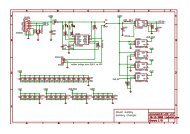
3 BLOCKDIAGRAM<br />
Analogue RF Interface Digital Control EEPROM<br />
PAD<br />
VREG<br />
V<br />
VDD<br />
Anticollision<br />
32 Bit<br />
Transponder<br />
RECT<br />
Cres<br />
DEMOD<br />
MOD<br />
Data<br />
In<br />
Read/Write<br />
Control<br />
Access<br />
Control<br />
64 Pages<br />
PAD<br />
CLK<br />
Data<br />
Out<br />
Clock<br />
EEPROM Interface<br />
Control<br />
RF Interface<br />
Control<br />
R/W<br />
Sequencer<br />
Charge Pump<br />
The <strong>HITAG</strong> S Transponder requires no internal power supply. The contactless interface generates the power<br />
supply and the system clock via the resonant circuitry by inductive coupling to the Read/Write Device (RWD).<br />
The interface also demodulates data that are transmitted from the RWD to the <strong>HITAG</strong> S Transponder, and<br />
modulates the magnetic field for data transmission from the <strong>HITAG</strong> S Transponder to the RWD.<br />
Data are stored in a non-volatile memory (EEPROM). The EEPROM has a memory capacity up to 2048 Bit<br />
and is <strong>org</strong>anised in 64 Pages consisting of 4 Bytes each (1 Page = 32 Bits).<br />
printed 16.10.02 8 Confidential
Philips Semiconductors Objective Specification Rev. 1.1, October 2002<br />
Functional Specification<br />
HTS IC H32/HTS IC H56/HTS IC H48<br />
4 ORDERING INFORMATION<br />
Type Name Memory Size Description Ordering Code<br />
HTS IC H32 01DW/V4<br />
32 Bit<br />
Sawn 8” wafer on foil (FFC), 150 µm, inked<br />
and mapped, with gold bumps<br />
xxxx xxx xxxxx<br />
HTS IC H56 01DW/V4<br />
256 Bit<br />
Sawn 8” wafer on foil (FFC), 150 µm, inked<br />
and mapped, with gold bumps<br />
HTS IC H48 01DW/V4<br />
2048 Bit<br />
Sawn 8” wafer on foil (FFC), 150 µm, inked<br />
and mapped, with gold bumps<br />
HTS MO H32 01DV 32 Bit MOA2 Package<br />
HTS MO H56 01DV 256 Bit MOA2 Package<br />
HTS MO H48 01DV 2048 Bit MOA2 Package<br />
HTS FC H32 01DV/VH 32 Bit Flip Chip Package, Hot Laminated<br />
HTS FC H56 01DV/VH 256 Bit Flip Chip Package, Hot Laminated<br />
HTS FC H48 01DV/VH 2048 Bit Flip Chip Package, Hot Laminated<br />
5 REFERENCE DOCUMENTS<br />
• General Quality Specification<br />
• General Specification for 8” Wafer<br />
• Bumped Wafer Specification<br />
• Addendum Bumped Wafer Specification HTS IC H32/ HTS IC H56/ HTS IC H48<br />
• Contactless Chip Card Module Specification<br />
• Addendum Contactless Chip Card Module Specification HTS MO H32/HTS MO H56/HTS MO H48<br />
• Flip Chip Package Specification FCP 2.1<br />
• Addendum Flip Chip Package Specification HTS FC H32/HTS FC H56/HTS FC H48<br />
printed 16.10.02 9 Confidential
Philips Semiconductors Objective Specification Rev. 1.1, October 2002<br />
Functional Specification<br />
HTS IC H32/HTS IC H56/HTS IC H48<br />
6 MEMORY ORGANISATION<br />
Block 1 Block 0<br />
Block 2<br />
Block 3<br />
Page<br />
Address<br />
0x00<br />
0x01<br />
0x02<br />
0x03<br />
0x04<br />
0x05<br />
0x06<br />
0x07<br />
0x08<br />
0x09<br />
0x0A<br />
0x0B<br />
0x0C<br />
0x0D<br />
0x0E<br />
0x0F<br />
0x10<br />
32 Bit<br />
Page 0<br />
Page 1<br />
Page 2<br />
Page 3<br />
Page 4<br />
Page 5<br />
Page 6<br />
Page 7<br />
Page 8<br />
Page 9<br />
Page10<br />
Page 11<br />
Page 12<br />
Page 13<br />
Page 14<br />
Page 15<br />
Page 16<br />
<strong>HITAG</strong> S Type<br />
H32 H56 H48<br />
Block 15<br />
0x3B<br />
0x3C<br />
0x3D<br />
0x3E<br />
0x3F<br />
Page 59<br />
Page 60<br />
Page 61<br />
Page 62<br />
Page 63<br />
The EEPROM has a memory capacity up to 2048 Bit and is <strong>org</strong>anised in 16 Blocks consisting of 4 Pages<br />
each for commands with Block access. A Page consists of 4 Bytes each (1 Page = 32 Bits) and is the<br />
smallest access unit.<br />
Addressing is done Page by Page (Page 0 up to 63) and access is gained either Page by Page or Block by<br />
Block entering the respective Page start address. In case of Block Read/Write access, the transponder is<br />
processed from the start Page address within one block to the end of the corresponding block.<br />
Three different types of <strong>HITAG</strong> S IC’s with different memory sizes as shown in the figure above are available.<br />
printed 16.10.02 10 Confidential
Philips Semiconductors Objective Specification Rev. 1.1, October 2002<br />
Functional Specification<br />
HTS IC H32/HTS IC H56/HTS IC H48<br />
6.1 Unique Identifier (UID)<br />
Page 0 contains the 32 Bit Unique Identifier (UID) which is programmed during the manufacturing process.<br />
Page 0 access: Read Only (RO)<br />
MSByte<br />
LSByte<br />
Page Address MSB LSBMSB LSB MSB LSBMSB LSB<br />
0x00 UID 3 UID 2 UID 1 UID 0<br />
6.2 <strong>HITAG</strong> S Plain Mode<br />
Page 1:<br />
In Plain Mode, Page 1 contains three configuration Bytes CON 0 to CON 2 and a reserved byte.<br />
MSByte<br />
LSByte<br />
Page Address MSB LSBMSB LSB MSB LSBMSB LSB<br />
0x01 Reserved CON 2 CON 1 CON 0<br />
Page 2 - 63:<br />
In Plain Mode, Pages 2 – 63 can be used to store user data.<br />
MSByte<br />
LSByte<br />
Page Address MSB LSB MSB LSB MSB LSBMSB LSB<br />
0x02 – 0x3F Data 3 Data 2 Data 1 Data 0<br />
Memory Map for <strong>HITAG</strong> S in Plain Mode:<br />
MSByte<br />
LSByte<br />
Page Address MSB LSBMSB LSB MSB LSBMSB LSB<br />
0x00 UID 3 UID 2 UID 1 UID 0<br />
0x01 Reserved CON 2 CON 1 CON 0<br />
0x02 Data 3 Data 2 Data 1 Data 0<br />
0x03 Data 3 Data 2 Data 1 Data 0<br />
printed 16.10.02 11 Confidential
Philips Semiconductors Objective Specification Rev. 1.1, October 2002<br />
Functional Specification<br />
HTS IC H32/HTS IC H56/HTS IC H48<br />
6.3 <strong>HITAG</strong> S Authentication Mode<br />
Page 1:<br />
In Authentication Mode, Page 1 contains three configuration Bytes CON 0 to CON 2 and the password high<br />
Byte PWDH 0.<br />
MSByte<br />
LSByte<br />
Page Address MSB LSBMSB LSB MSB LSBMSB LSB<br />
0x01 PWDH 0 CON 2 CON 1 CON 0<br />
Page 2:<br />
In Authentication Mode, Page 2 contains the password low Bytes PWDL 0 and PWDL 1 and the key high<br />
Bytes KEYH 0 and KEYH 1.<br />
MSByte<br />
LSByte<br />
Page Address MSB LSBMSB LSB MSB LSBMSB LSB<br />
0x02 KEYH 1 KEYH 0 PWDL 1 PWDL 0<br />
Page 3:<br />
In Authentication Mode, Page 3 contains the key low Bytes KEYL 0 - KEYL 3.<br />
MSByte<br />
LSByte<br />
Page Address MSB LSBMSB LSB MSB LSBMSB LSB<br />
0x03 KEYL 3 KEYL 2 KEYL 1 KEYL 0<br />
Page 4 - 63:<br />
In Authentication Mode, Pages 4 – 63 can be used to store user data.<br />
MSByte<br />
LSByte<br />
Page Address MSB LSBMSB LSB MSB LSBMSB LSB<br />
0x04 – 0x3F Data 3 Data 2 Data 1 Data 0<br />
Memory Map for <strong>HITAG</strong> S in Authentication Mode:<br />
MSByte<br />
LSByte<br />
Page Address MSB LSBMSB LSB MSB LSBMSB LSB<br />
0x00 UID 3 UID 2 UID 1 UID 0<br />
0x01 PWDH 0 CON 2 CON 1 CON 0<br />
0x02 KEYH 1 KEYH 0 PWDL 1 PWDL 0<br />
0x03 KEYL 3 KEYL 2 KEYL 1 KEYL 0<br />
0x04 Data 3 Data 2 Data 1 Data 0<br />
0x05 Data 3 Data 2 Data 1 Data 0<br />
printed 16.10.02 12 Confidential
Philips Semiconductors Objective Specification Rev. 1.1, October 2002<br />
Functional Specification<br />
HTS IC H32/HTS IC H56/HTS IC H48<br />
7 FUNCTIONAL DESCRIPTION<br />
7.1 Basic System Configuration<br />
The following block diagram shows in principle the <strong>HITAG</strong> system configuration.<br />
Read / Write Device (RWD)<br />
Oscillator Modulator Driver<br />
Host<br />
Interface<br />
Control<br />
Signal & Data<br />
Processing<br />
RWD<br />
Antenna<br />
M<br />
Amplifier<br />
Demodulator<br />
Filter<br />
<strong>HITAG</strong> S<br />
Transponder<br />
Antenna<br />
A control and data processing unit controls the modulation of the carrier signal and processes data coming<br />
back from the demodulator circuit.<br />
7.2 Energy Transmission<br />
Passive transponders must somehow be supplied with energy to be able to operate. In the <strong>HITAG</strong> System,<br />
this is achieved by using the principle of a loose coupled transformer:<br />
RWD<br />
Antenna<br />
M<br />
Transponder<br />
Antenna<br />
Energy<br />
Data<br />
The RWD antenna generates a magnetic field. Some of the generated magnetic flux flows through the<br />
transponder antenna and induces a voltage there. The voltage drives a current and the transponder will start<br />
operating. As this current will be very small when the transponder is far away from the antenna, the <strong>HITAG</strong> S<br />
Transponder IC is designed for low power consumption.<br />
The principle of a loose coupled transformer enables also a bi-directional data transmission.<br />
printed 16.10.02 13 Confidential
Philips Semiconductors Objective Specification Rev. 1.1, October 2002<br />
Functional Specification<br />
HTS IC H32/HTS IC H56/HTS IC H48<br />
7.3 Data Transmission: Transponder fi Read/Write Device<br />
For data transmission from the <strong>HITAG</strong> S Transponder to the RWD, the implemented method is called 'load<br />
modulation'. Here the <strong>HITAG</strong> S Transponder continuously changes the load on the magnetic field, by in<br />
principle turn on/off a resistor, according to the information to transmit. Alteration of the magnetic field is<br />
detected by the receiver of the RWD.<br />
Data<br />
Coded<br />
Data (MC)<br />
1 1 0<br />
Voltage<br />
on<br />
Transponder<br />
Antenna<br />
Voltage<br />
on<br />
RWD<br />
Antenna<br />
The modulation ratio of the RWD antenna voltage depends on the coupling factor of the antenna<br />
configuration (RWD antenna size, transponder antenna size, distance between the antennas,...).<br />
7.3.1 CODING<br />
Three different coding techniques for different States and Modes of the <strong>HITAG</strong> S Transponder IC are used<br />
(see also chapters “Command Set" and “Transponder Talks First (TTF) Mode”):<br />
• AC: AntiCollision Coding in Init State<br />
• MC: Manchester Coding in Selected State and in Transponder Talks First State<br />
• BC: Biphase Coding in Transponder Talks First State<br />
DATA 1 0 1 1 1 0 0 1<br />
DATA RATE<br />
AC<br />
MC<br />
BC<br />
A high level of the above coding signals means the physical state ‘modulator on’ (field loaded), a low level<br />
means ‘modulator off’ (field unloaded).<br />
printed 16.10.02 14 Confidential
Philips Semiconductors Objective Specification Rev. 1.1, October 2002<br />
Functional Specification<br />
HTS IC H32/HTS IC H56/HTS IC H48<br />
7.3.2 DATA RATE<br />
The data rate for <strong>HITAG</strong> S Transponder in Reader Talks First (RTF) Mode depends on the corresponding<br />
UID REQUEST xx command.<br />
For Tag Talks First (TTF) Mode the data rate can be defined by configuration.<br />
Mode Coding Bit Rate Bit Length<br />
<strong>HITAG</strong> S<br />
RTF<br />
Mode<br />
<strong>HITAG</strong> S<br />
TTF<br />
Mode<br />
AC<br />
MC<br />
MC<br />
Biphase<br />
2 kBit/s 64 T 0<br />
4 kBit/s 32 T 0<br />
4 kBit/s 32 T 0<br />
8 kBit/s 16 T 0<br />
2 kBit/s 64 T 0<br />
4 kBit/s 32 T 0<br />
8 kBit/s 16 T 0<br />
2 kBit/s 64 T 0<br />
4 kBit/s 32 T 0<br />
T 0 ...Carrier period time ( 1 / 125kHz = 8 µs nominal)<br />
8 kBit/s 16 T 0<br />
7.4 Data Transmission: Read/Write Device fi Transponder<br />
Data are transmitted to the transponder using Amplitude Shift Keying (ASK) modulation with a modulation<br />
index of 100 %. When the field is switched off, the physical state is named low field, otherwise high field.<br />
7.4.1 CODING<br />
Binary Pulse Length Coding (BPLC) is used to encode the data stream.<br />
All coded data Bits and the end of frame (EOF) condition start with a low field of length T g .<br />
Afterwards the field is switched on again.<br />
• ‘0’ and ‘1’ can be distinguished by the duration of T[0] and T[1].<br />
• The end of the data transmission is characterised by a end of frame condition.<br />
The following figure shows the data transmission from the Read/Write Device to the transponder.<br />
printed 16.10.02 15 Confidential
Philips Semiconductors Objective Specification Rev. 1.1, October 2002<br />
Functional Specification<br />
HTS IC H32/HTS IC H56/HTS IC H48<br />
T[0]<br />
T[1]<br />
T g<br />
T EOF<br />
Data<br />
0 0 1 1 EOF<br />
Coded<br />
Data<br />
Voltage<br />
on<br />
RWD<br />
Antenna<br />
Voltage<br />
on<br />
Transponder<br />
Antenna<br />
Symbol Description Duration<br />
T g Gap time 4..10 T 0 *)<br />
T[0] Logic 0 Bit length 18..22 T 0 *)<br />
T[1] Logic 1 Bit length 26..30 T 0 *)<br />
T EOF Duration for end of frame condition > 36 T 0<br />
*) This application specific values must be within this frame, but have to be optimised for each application<br />
depending on rise and decay times of the RWD antenna voltage and the transponder antenna quality<br />
factor!<br />
T 0<br />
Carrier period time ( 1 / 125kHz = 8 µs nominal)<br />
The average Bit rate from the Read/Write Device to the <strong>HITAG</strong> S Transponder therefore is:<br />
Bit rate =<br />
Note:<br />
2<br />
T 0<br />
[ ] + T[ 1]<br />
=<br />
5.2 kBit / s<br />
The end of each data sequence from the Read/Write Device to the <strong>HITAG</strong> S Transponder<br />
has to be a EOF condition.<br />
printed 16.10.02 16 Confidential
Philips Semiconductors Objective Specification Rev. 1.1, October 2002<br />
Functional Specification<br />
HTS IC H32/HTS IC H56/HTS IC H48<br />
7.4.2 MODULATION DETAILS<br />
T f<br />
T g<br />
T[0]<br />
T r<br />
a<br />
y<br />
b<br />
x<br />
Envelope of RWD Antenna Voltage<br />
x = 0.15 a, y = 0.95 a<br />
m = (a - b) / (a + b).....Modulation index<br />
Symbol Min Max<br />
m 90 % 100 %<br />
T f 0 t.b.d.<br />
T r 0 t.b.d.<br />
The following table shows two examples of modulation timing parameters for typical short- and long range<br />
applications.<br />
Symbol Short range application Long range application<br />
T g 6 T 0 9 T 0<br />
T[0] 20 T 0 22 T 0<br />
T[1] 28 T 0 28 T 0<br />
T f 3 T 0 4 T 0<br />
T r 5 T 0 6 T 0<br />
printed 16.10.02 17 Confidential
Philips Semiconductors Objective Specification Rev. 1.1, October 2002<br />
Functional Specification<br />
HTS IC H32/HTS IC H56/HTS IC H48<br />
8 CONFIGURATION<br />
8.1 Configuration Page<br />
Memory Page 1 contains the three configuration Bytes CON 0, CON 1 and CON 2 (see ‘Memory<br />
Organisation’).<br />
Changes on the Configuration Bytes are only active after a power on reset of the <strong>HITAG</strong> S Transponder.<br />
CON0: Memory Type Information<br />
CON 0<br />
MSB<br />
LSB<br />
RES 5 RES 4 RES 3 RES 2 RES 1 RES 0 MEMT 1 MEMT 0<br />
The following table describes the Memory Type Bits MEMT 0 and MEMT 1 of configuration byte CON 0.<br />
MEMT 1 MEMT 0 Memory Type<br />
0 0 32 Bit<br />
0 1 256 Bit<br />
1 0 2048 Bit<br />
1 1 Reserved<br />
Bits RES 0 to RES 5 are reserved for future use.<br />
Only Read access to configuration byte CON 0 is possible.<br />
CON 1: Mode and Lock Bits<br />
CON 1<br />
MSB<br />
LSB<br />
AUT TTFC TTFDR 1 TTFDR 0 TTFM 1 TTFM 0 LCON LKP<br />
If the Authentication Bit AUT = ‘0’ the <strong>HITAG</strong> S Transponder IC is configured in Plain Mode and can be<br />
Selected directly by the SELECT (UID) command and the corresponding UID. For Bit AUT = ‘1’ the <strong>HITAG</strong> S<br />
Transponder IC is configured in Authentication Mode and can only be Selected with the SELECT (UID)<br />
command and a following secure CHALLENGE sequence (see also chapters ‘State Diagram’ and ‘Command<br />
Set’).<br />
AUT<br />
<strong>HITAG</strong> S Mode<br />
0 Plain<br />
1 Authentication<br />
The Transponder Talks First Coding Bit TTFC defines the used coding during transmitting data to the RWD.<br />
This effects the TTF State only.<br />
printed 16.10.02 18 Confidential
Philips Semiconductors Objective Specification Rev. 1.1, October 2002<br />
Functional Specification<br />
HTS IC H32/HTS IC H56/HTS IC H48<br />
TTFC Coding in TTF State<br />
0 Manchester<br />
1 Biphase<br />
The Transponder Talks First Data Rate Bits TTFDR 0 and TTFDR 1 define the used data rate during<br />
transmitting data to the RWD. This effects the TTF State only.<br />
TTFDR 1 TTFDR 0 Data rate in TTF State<br />
0 0 4 kBit<br />
0 1 8 kBit<br />
1 0 2 kBit<br />
1 1 2 kBit and Pigeon Race Standard<br />
The Transponder Talks First Mode Bits TTFM 0 and TTFM 1 defines the number of Pages continuously<br />
transmitted to the RWD. This effects the TTF State only.<br />
TTFM 1 TTFM 0 Pages transmitted in TTF State<br />
0 0 TTF Mode disabled (= RTF Mode)<br />
0 1 Page 4, Page 5<br />
1 0 Page 4, Page 5, Page 6, Page 7<br />
1 1 Page 4<br />
The Lock Configuration Bit LCON defines the access rights of the configuration Bytes CON 1 and CON 2.<br />
This Bit is one time programmable (OTP).<br />
LCON Access right CON 1 and CON 2<br />
0 Read / Write<br />
1<br />
CON 1: Read Only<br />
CON 2: OTP<br />
The Lock Key and Password Bit LKP defines the access rights of the PWDH 0 Byte of Page 1, password low<br />
Bytes and key high Bytes of Page 2 and key low Bytes of Page 3 when configured in Authentication Mode. In<br />
Plain Mode this Bit can be used to lock the user data of Page 2 and Page 3.<br />
LKP Access right key and password/Page 2 and Page 3<br />
0 Read / Write<br />
1<br />
Read Only in Plain Mode<br />
No Access in Authentication Mode<br />
Attention: In order to prevent further access to key and password, the following procedure must take place:<br />
After setting Bit LKP to ‘1’ the Lock Configuration Bit LCON must be set to ‘1’, because the Bit LKP has no<br />
OTP functionality!<br />
printed 16.10.02 19 Confidential
Philips Semiconductors Objective Specification Rev. 1.1, October 2002<br />
Functional Specification<br />
HTS IC H32/HTS IC H56/HTS IC H48<br />
CON 2: Memory Lock Bits<br />
CON 2<br />
MSB<br />
LSB<br />
LCK 7 LCK 6 LCK 5 LCK 4 LCK 3 LCK 2 LCK 1 LCK 0<br />
Bit Function Access rights Comment<br />
LCK 7 Lock Page 4 and Page 5<br />
LCK 6 Lock Page 6 and Page 7<br />
LCK 5 Lock Page 8 – Page 11<br />
LCK 4 Lock Page 12 – Page 15<br />
LCK 3 Lock Page 16 – Page 23<br />
LCK 2 Lock Page 24 – Page 31<br />
LCK 1 Lock Page 32 – Page 47<br />
LCK 0 Lock Page 48 – Page 63<br />
0...Read / Write<br />
1...Read Only<br />
0...Read / Write<br />
1...Read Only<br />
0...Read / Write<br />
1...Read Only<br />
0...Read / Write<br />
1...Read Only<br />
0...Read / Write<br />
1...Read Only<br />
0...Read / Write<br />
1...Read Only<br />
0...Read / Write<br />
1...Read Only<br />
0...Read / Write<br />
1...Read Only<br />
OTP if LCON = ‘1’<br />
If Pigeon Race Standard is enabled<br />
(TTFDR 0 = TTFDR 1 = ‘1’) 16 Bits<br />
(Data 3 u. Data 2) of Page 5 remain still<br />
Read/Write accessible for LCK 7 = ‘1’<br />
OTP if LCON = ‘1’<br />
OTP if LCON = ‘1’<br />
OTP if LCON = ‘1’<br />
OTP if LCON = ‘1’<br />
OTP if LCON = ‘1’<br />
OTP if LCON = ‘1’<br />
OTP if LCON = ‘1’<br />
printed 16.10.02 20 Confidential
Philips Semiconductors Objective Specification Rev. 1.1, October 2002<br />
Functional Specification<br />
HTS IC H32/HTS IC H56/HTS IC H48<br />
8.2 Delivery Configuration<br />
8.2.1 <strong>HITAG</strong> S32<br />
This delivery configuration is valid for the following <strong>HITAG</strong> S 32 types:<br />
HTS IC H32 01 DW/V4<br />
HTS MO H32 01 DV<br />
HTS FC H32 01 DV/VH<br />
MSByte<br />
LSByte<br />
MSB LSB MSB LSBMSB LSB MSB LSB<br />
UID 3 UID 2 UID 1 UID 0<br />
The 32 Bit Unique Identifier (UID) is programmed during the manufacturing process.<br />
Access rights: Read Only (RO)<br />
On a Select (UID) command the <strong>HITAG</strong> S32 Transponder IC sends back three Reserved Bytes and the Byte<br />
CON 0 containing the Memory Type Information.<br />
MSByte<br />
LSByte<br />
MSB LSB MSB LSBMSB LSB MSB LSB<br />
X X X CON 0<br />
CON 0<br />
MSB<br />
LSB<br />
X X X X X X 0 0<br />
The content of Bits and Bytes marked with ‘X’ are not defined at delivery!<br />
8.2.2 <strong>HITAG</strong> S256<br />
This delivery configuration is valid for the following <strong>HITAG</strong> S 256 types:<br />
HTS IC H56 01 DW/V4<br />
HTS MO H56 01 DV<br />
HTS FC H56 01 DV/VH<br />
MSByte<br />
LSByte<br />
Page Address MSB LSBMSB LSB MSB LSBMSB LSB<br />
0x00 UID 3 UID 2 UID 1 UID 0<br />
0x01 0xAA 0x00 0x00 CON 0<br />
0x02 0x4E 0x4F 0x54 0x48<br />
0x03 0x52 0x4B 0x49 0x4D<br />
0x04 X X X X<br />
0x05 X X X X<br />
0x06 X X X X<br />
0x07 X X X X<br />
printed 16.10.02 21 Confidential
Philips Semiconductors Objective Specification Rev. 1.1, October 2002<br />
Functional Specification<br />
HTS IC H32/HTS IC H56/HTS IC H48<br />
MSB<br />
CON 0<br />
X X X X X X 0 1<br />
The content of Bits and Bytes marked with ‘X’ are not defined at delivery!<br />
• The 32 Bit Unique Identifier (UID) is programmed during the manufacturing process.<br />
• Modes: Reader Talks First (RTF), Plain<br />
• Access Rights:<br />
UID: Read Only<br />
Page 1: Read/Write with exception of byte CON 0 (Read Only)<br />
Page 2 – Page 7: Read/Write<br />
LSB<br />
8.2.3 <strong>HITAG</strong> S2048<br />
This delivery configuration is valid for the following <strong>HITAG</strong> S 2048 types:<br />
HTS IC H48 01 DW/V4<br />
HTS MO H48 01 DV<br />
HTS FC H48 01 DV/VH<br />
MSByte<br />
LSByte<br />
Page Address MSB LSBMSB LSB MSB LSBMSB LSB<br />
0x00 UID 3 UID 2 UID 1 UID 0<br />
0x01 0xAA 0x00 0x00 CON 0<br />
0x02 0x4E 0x4F 0x54 0x48<br />
0x03 0x52 0x4B 0x49 0x4D<br />
0x04 X X X X<br />
0x05 X X X X<br />
0x3E X X X X<br />
0x3F X X X X<br />
MSB<br />
CON 0<br />
X X X X X X 1 0<br />
The content of Bits and Bytes marked with ‘X’ are not defined at delivery!<br />
• The 32 Bit Unique Identifier (UID) is programmed during the manufacturing process.<br />
• Modes: Reader Talks First (RTF), Plain<br />
• Access Rights:<br />
UID: Read Only<br />
Page 1: Read/Write with exception of byte CON 0 (Read Only)<br />
Page 2 – Page 63: Read/Write<br />
LSB<br />
printed 16.10.02 22 Confidential
Philips Semiconductors Objective Specification Rev. 1.1, October 2002<br />
Functional Specification<br />
HTS IC H32/HTS IC H56/HTS IC H48<br />
9 PROTOCOL TIMING<br />
9.1 <strong>HITAG</strong> S Transponder Start up Time<br />
Coded<br />
Data<br />
RWD<br />
t start-up<br />
Voltage<br />
on<br />
RWD<br />
Antenna<br />
y<br />
a<br />
y = 0.95 a<br />
After switching on the powering field, the Read/Write Device has to wait t start-up before sending the first<br />
command. After t start-up the <strong>HITAG</strong> S Transponder IC is in Ready State .<br />
MIN TYP MAX Unit<br />
t start-up 245 t.b.d. T 0<br />
9.2 <strong>HITAG</strong> S Transponder Reset Time<br />
The powering field must be switched off for at least t reset = 2 ms to generate a reset of the <strong>HITAG</strong> S IC and to<br />
enter it into Power Off State.<br />
Voltage<br />
on<br />
RWD<br />
Antenna<br />
x<br />
t reset<br />
a<br />
x = 0.15 a<br />
MIN TYP MAX Unit<br />
t reset 2 ms<br />
printed 16.10.02 23 Confidential
Philips Semiconductors Objective Specification Rev. 1.1, October 2002<br />
Functional Specification<br />
HTS IC H32/HTS IC H56/HTS IC H48<br />
9.3 <strong>HITAG</strong> S Transponder waiting time before transmitting a response after receiving an EOF<br />
t wresp<br />
Data<br />
RWD<br />
Coded<br />
Data<br />
RWD<br />
1 EOF<br />
Voltage<br />
on<br />
RWD<br />
Antenna<br />
Voltage<br />
on<br />
Transponder<br />
Antenna<br />
Coded<br />
Data(MC)<br />
Transponder<br />
Data<br />
Transponder<br />
SOF<br />
1<br />
When receiving a End of Frame (EOF) condition from the Read/Write Device, the transponder waits t wresp<br />
before transmitting data.<br />
MIN TYP MAX Unit<br />
t wresp 204 208 212 T 0<br />
9.4 <strong>HITAG</strong> S Transponder programming time<br />
t prog<br />
Write Data<br />
EOF<br />
RWD<br />
Transponder<br />
SOF<br />
ACK<br />
When receiving the EOF of the write data from the Read/Write Device, the transponder waits t prog before<br />
transmitting the SOF and acknowledge to confirm correct programming.<br />
MIN TYP MAX Unit<br />
t prog 716 721 726 T 0<br />
printed 16.10.02 24 Confidential
Philips Semiconductors Objective Specification Rev. 1.1, October 2002<br />
Functional Specification<br />
HTS IC H32/HTS IC H56/HTS IC H48<br />
9.5 <strong>HITAG</strong> S Transponder waiting time before transmitting data in TTF Mode<br />
Coded<br />
Data<br />
RWD<br />
t TTF<br />
Voltage<br />
on<br />
RWD<br />
Antenna<br />
y<br />
a<br />
Voltage<br />
on<br />
Transponder<br />
Antenna<br />
Coded<br />
Data<br />
(MC)<br />
Data 1 1<br />
y = 0.95 a<br />
After switching on the powering field, the <strong>HITAG</strong> S Transponder waits a time t TTF before transmitting data if it<br />
is configured in TTF Mode.<br />
MIN TYP MAX Unit<br />
t TTF 580 610 640 T 0<br />
9.6 <strong>HITAG</strong> S Transponder Mode switching window<br />
Coded<br />
Data<br />
RWD<br />
t start-up<br />
UID REQUEST xx<br />
t switch<br />
Voltage<br />
y<br />
on<br />
RWD<br />
Antenna<br />
a<br />
Within the time t switch a <strong>HITAG</strong> S Transponder configured in TTF Mode can be switched into RTF Mode by a<br />
UID REQUEST xx command. The <strong>HITAG</strong> S Transponder responds to this command with the UID and<br />
changes into Init State .<br />
MIN TYP MAX Unit<br />
t switch t.b.d. 320 t.b.d T 0<br />
printed 16.10.02 25 Confidential
Philips Semiconductors Objective Specification Rev. 1.1, October 2002<br />
Functional Specification<br />
HTS IC H32/HTS IC H56/HTS IC H48<br />
9.7 Read/Write Device waiting time before sending a subsequent command<br />
Data<br />
RWD<br />
t wcom<br />
0<br />
1<br />
Coded<br />
Data<br />
RWD<br />
Voltage<br />
on<br />
RWD<br />
Antenna<br />
Voltage<br />
on<br />
Transponder<br />
Antenna<br />
Coded<br />
Data(MC)<br />
Transponder<br />
Data<br />
Transponder<br />
1 0<br />
When the Read/Write Device has received the response from the <strong>HITAG</strong> S Transponder to a previous<br />
command, the RWD has to wait a time t wcom before sending a subsequent command or Write data after a<br />
Write command.<br />
Data transmitted to the <strong>HITAG</strong> S Transponder within t wcom , will not be recognised.<br />
MIN TYP MAX Unit<br />
t wcom 90 T 0<br />
printed 16.10.02 26 Confidential
Philips Semiconductors Objective Specification Rev. 1.1, October 2002<br />
Functional Specification<br />
HTS IC H32/HTS IC H56/HTS IC H48<br />
10 STATE DIAGRAM<br />
10.1 General description of State s<br />
Power Off<br />
The powering magnetic field is switched off or the <strong>HITAG</strong> S Transponder is out of field<br />
Ready<br />
After start up phase, the <strong>HITAG</strong> S Transponder is ready to receive the first command.<br />
Init<br />
The <strong>HITAG</strong> S Transponder enters this State after the first UID REQUEST xx command.<br />
In this State the Response Protocol Mode (see chapter ‘Command Set’) may be changed by further<br />
UID REQUEST xx commands.<br />
If there are several <strong>HITAG</strong> S Transponders in the field of the RWD antenna at the same time, the<br />
AC SEQUENCE can be started to determine the UID of every <strong>HITAG</strong> S Transponder.<br />
Authenticate<br />
The <strong>HITAG</strong> S Transponder enters this State after a valid SELECT (UID) command when configured in<br />
Authentication Mode.<br />
After a encrypted CHALLENGE Authentication the <strong>HITAG</strong> S Transponder changes into the Selected State.<br />
Selected<br />
The <strong>HITAG</strong> S Transponder enters this State after a valid SELECT (UID) command when configured in Plain<br />
Mode or by a SELECT (UID) and CHALLENGE sequence when configured in Authentication Mode.<br />
Only one <strong>HITAG</strong> S Transponder in the field of the RWD antenna can be Selected at the same time.<br />
In this State, Read and Write operations from and to the memory are possible.<br />
Quiet<br />
The <strong>HITAG</strong> S Transponder enters this State after a SELECT_QUIET command in Init State or a QUIET<br />
command in Selected State.<br />
In this State, the <strong>HITAG</strong> S Transponder will not answer to any command.<br />
Switching off the powering magnetic field or moving the <strong>HITAG</strong> S Transponder out of field enters it into the<br />
Power Off State.<br />
Transponder Talks First (TTF)<br />
The <strong>HITAG</strong> S Transponder enters this State when configured in TTF Mode and without receiving a<br />
UID REQUEST xx command within the Mode switch window.<br />
In this State, the <strong>HITAG</strong> S Transponder continuously transmits data with configurable data coding, data rate<br />
and data length.<br />
printed 16.10.02 27 Confidential
Philips Semiconductors Objective Specification Rev. 1.1, October 2002<br />
Functional Specification<br />
HTS IC H32/HTS IC H56/HTS IC H48<br />
10.2 <strong>HITAG</strong> S32<br />
Power Off<br />
In Field<br />
Ready<br />
Any other command<br />
or<br />
transmission error<br />
Transmission<br />
error<br />
Init<br />
UID REQUEST xx<br />
UID REQUEST xx<br />
AC SEQUENCE<br />
SELECT (UID) command with wrong UID<br />
SELECT_QUIET (UID) command with wrong UID<br />
Any other command<br />
SELECT (UID)<br />
Selected<br />
SELECT_QUIET (UID)<br />
QUIET<br />
Quiet<br />
Any command<br />
Note:<br />
Switching off the powering magnetic field or moving the <strong>HITAG</strong> S Transponder out of the RWD antenna field,<br />
enters the <strong>HITAG</strong> S Transponder into the Power Off State, independently of its previous State.<br />
printed 16.10.02 28 Confidential
Philips Semiconductors Objective Specification Rev. 1.1, October 2002<br />
Functional Specification<br />
HTS IC H32/HTS IC H56/HTS IC H48<br />
10.3 <strong>HITAG</strong> S256 and <strong>HITAG</strong> S2048<br />
Power Off<br />
A : TTF Mode enabled and UID REQUESTxx<br />
command not sent within switch window<br />
Transponder<br />
Talks<br />
First<br />
A<br />
In Field<br />
Ready<br />
B : TTF Mode enabled : UID REQUESTxx<br />
command sent within switch window<br />
or<br />
TTF Mode disabled : UID REQUESTxx<br />
Bit AUT: See chapter ’Configuration’<br />
Any command<br />
Any other command,<br />
transmission error or<br />
wrong keys<br />
B<br />
lnit<br />
Transmission<br />
error<br />
UID REQUEST xx<br />
AC SEQUENCE<br />
SELECT (UID) command with wrong UID<br />
SELECT_QUIET (UID) command with wrong UID<br />
Any other command<br />
Authenticate<br />
SELECT (UID)<br />
&<br />
AUT=1<br />
CHALLENGE<br />
SELECT (UID)<br />
&<br />
AUT = 0<br />
Any other command<br />
or transmission error<br />
Selected<br />
READ PAGE<br />
READ BLOCK<br />
WRITE PAGE<br />
WRITE BLOCK<br />
SELECT_QUIET (UID)<br />
QUIET<br />
Quiet<br />
Any command<br />
Note:<br />
Switching off the powering magnetic field or moving the <strong>HITAG</strong> S Transponder out of the RWD antenna field,<br />
enters the <strong>HITAG</strong> S Transponder into the Power Off State, independently of its previous State.<br />
printed 16.10.02 29 Confidential
Philips Semiconductors Objective Specification Rev. 1.1, October 2002<br />
Functional Specification<br />
HTS IC H32/HTS IC H56/HTS IC H48<br />
11 COMMAND SET<br />
11.1 General Comments<br />
For <strong>HITAG</strong> S 32 only the commands described in the corresponding State diagram are valid commands.<br />
11.2 UID REQUEST xx<br />
MSB<br />
LSB<br />
RWD: UID REQUEST xx EOF<br />
LSByte<br />
MSByte<br />
MSB LSB MSB LSB MSB LSB MSB LSB<br />
Transponder: t wresp SOF UID 0 UID 1 UID 2 UID 3<br />
N = 1.............8 9....k...16 17.......24 25.......32<br />
N...Bit position<br />
k...Any collision position (see command AC SEQUENCE)<br />
After the RWD transmits this command, all <strong>HITAG</strong> S Transponders located in the field of the RWD antenna<br />
respond with a start of frame pattern followed by the corresponding 32 Bit UID. The complete response of<br />
the <strong>HITAG</strong> S Transponder is transmitted in Anticollision Coding (AC, see section 7.3.1 Coding).<br />
Coding: MSB LSB Response Protocol Mode<br />
UID REQUEST Std 0 0 1 1 0 Standard<br />
UID REQUEST Adv 1 1 0 0 x Advanced<br />
UID REQUEST FAdv 1 1 0 1 0 Fast Advanced<br />
x... can be ‘0’ or ‘1’<br />
The Response Protocol Mode defined by the corresponding UID Request command determines the coding,<br />
data rate and the SOF pattern of the <strong>HITAG</strong> S Transponder response.<br />
Response Protocol Mode SOF Coding Data Rate<br />
Standard ‘1’ AC 2 kBit/s<br />
Advanced ‘111’ AC 2 kBit/s<br />
Fast Advanced ‘111’ AC 4 kBit/s<br />
A <strong>HITAG</strong> S Transponder in Ready State changes into Init State after receiving a correct UID REQUEST xx<br />
command.<br />
A <strong>HITAG</strong> S Transponder being already in Init State remains in Init State after receiving a further correct<br />
UID REQUEST xx command.<br />
Always the latest UID REQUEST xx command defines the Response Protocol Mode for the following<br />
commands.<br />
printed 16.10.02 30 Confidential
Philips Semiconductors Objective Specification Rev. 1.1, October 2002<br />
Functional Specification<br />
HTS IC H32/HTS IC H56/HTS IC H48<br />
11.3 AC SEQUENCE<br />
If more than one <strong>HITAG</strong> S Transponder is in the field of the antenna a special designed RWD recognises the<br />
first collision at the Bit position N = k of the UID response. As a result the RWD starts an Anticollision<br />
Sequence (AC SEQUENCE).<br />
This command consists of a 5 Bit number (k4 to k0) with the Bit position k where the collision occurred<br />
followed by (k - 1) Bits of the recognised UID and a Bit (one or zero) at the collision position.<br />
An 8 Bit CRC (cyclic redundancy check) of this sequence is also sent to the transponders.<br />
MSB LSB 1..............................k MSB LSB<br />
RWD: k4 k3 k2 k1 k0 k Bits of UID CRC 8 EOF<br />
Transponder: t wresp SOF (32 – k) Bits of UID<br />
N =<br />
k+1...............................................32<br />
After transmitting this command, all <strong>HITAG</strong> S Transponders which first k Bits of the own UID match with the k<br />
received UID Bits, answer with the SOF and the rest of their own UID.<br />
If a collision occurs again the described cycle has to be repeated until one UID is determined.<br />
The complete response of the <strong>HITAG</strong> S Transponder is transmitted in Anticollision Coding (AC).<br />
Response Protocol Mode SOF Coding Data Rate<br />
Standard ‘1’ AC 2 kBit/s<br />
Advanced ‘111’ AC 2 kBit/s<br />
Fast Advanced ‘111’ AC 4 kBit/s<br />
During the AC SEQUENCE commands the <strong>HITAG</strong> S Transponder stays in Init State . Even those <strong>HITAG</strong> S<br />
Transponders where the k received Bits of the UID do not match remain in Init State.<br />
11.4 SELECT (UID)<br />
The SELECT (UID) command consists of 5 Zero-Bits followed by the determined 32 Bit UID and an 8 Bit<br />
Cyclic Redundancy Check (CRC). The selected transponder then responds with a start of frame pattern<br />
(SOF) followed by the content of the Configuration Page and dependent on the Response Protocol Mode<br />
with an 8 Bit CRC.<br />
LSByte<br />
MSByte<br />
MSB LSB MSB LSB MSB LSB MSB LSB MSB LSB<br />
RWD: 00000 UID 0 UID 1 UID 2 UID 3 CRC 8 EOF<br />
LSByte<br />
MSByte<br />
MSB LSB MSB LSB MSB LSB MSB LSB MSB LSB<br />
Transponder: t wresp SOF CON 0 CON 1 CON 2 Reserved CRC 8<br />
The complete response of the <strong>HITAG</strong> S Transponder is transmitted in Manchester Coding (MC).<br />
printed 16.10.02 31 Confidential
Philips Semiconductors Objective Specification Rev. 1.1, October 2002<br />
Functional Specification<br />
HTS IC H32/HTS IC H56/HTS IC H48<br />
In Plain Mode the MSByte of Page 1 is a Reserved Byte, in Authentication Mode this Byte contains the<br />
password high Byte PWDH 0. At the response on a SELECT (UID) command of a <strong>HITAG</strong> S Transponder<br />
configured in Authentication Mode (Bit AUT = 1, keys and password locked), this PWDH 0 Byte is dissolved<br />
by 8 One Bits.<br />
Response Protocol Mode SOF CRC 8 Coding Data Rate<br />
Standard ‘1’ no MC 4 kBit/s<br />
Advanced ‘111111’ yes MC 4 kBit/s<br />
Fast Advanced ‘111111’ yes MC 8 kBit/s<br />
In Plain Mode (Bit AUT = 0) the <strong>HITAG</strong> S Transponder changes into Selected State after receiving a correct<br />
SELECT (UID) command<br />
In Authentication Mode (Bit AUT = 1) the <strong>HITAG</strong> S Transponder changes into Authenticate State after<br />
receiving a correct SELECT (UID) command and waits for the CHALLENGE command.<br />
11.5 CHALLENGE<br />
By means of the response of the SELECT (UID) command the RWD recognises that the <strong>HITAG</strong> S<br />
Transponder is configured in Authentication Mode (Bit AUT = 1) and starts the encrypted Challenge<br />
sequence.<br />
MSB LSB MSB LSB<br />
RWD: 32 Bit RND 32 Bit Secret Data EOF<br />
MSB LSB MSB LSB MSB LSB MSB LSB MSB LSB<br />
Transponder: t wresp SOF CON 2 PWDH 0 PWDL 0 PWDL 1 CRC 8<br />
32 Bit Secret Response<br />
The Read/Write Device sends a 32 Bit Random Number (RND) and a 32 Bit secret data stream to the<br />
transponder. In order to perform the secret data stream, the Philips security coprocessor HT RC130 is<br />
required. If the received secret data stream corresponds with the secret data stream calculated by the<br />
<strong>HITAG</strong> S Transponder, a 32 Bit Secret Response (secret data stream encrypting the configuration byte<br />
CON 2, password high byte PWDH 0 and password low Bytes PWDL 0 and PWDL 1) is transmitted after the<br />
SOF.<br />
The response of the <strong>HITAG</strong> S Transponder is transmitted in Manchester Coding (MC).<br />
Response Protocol Mode SOF CRC 8 Coding Data Rate<br />
Standard ‘1’ no MC 4 kBit/s<br />
Advanced ‘111111’ yes MC 4 kBit/s<br />
Fast Advanced ‘111111’ yes MC 8 kBit/s<br />
A <strong>HITAG</strong> S Transponder configured in Authentication Mode changes from Authenticate State into Selected<br />
State only after a correct CHALLENGE Sequence.<br />
printed 16.10.02 32 Confidential
Philips Semiconductors Objective Specification Rev. 1.1, October 2002<br />
Functional Specification<br />
HTS IC H32/HTS IC H56/HTS IC H48<br />
11.6 SELECT_QUIET (UID)<br />
With this command a <strong>HITAG</strong> S Transponder in Init State can be directly entered into the Quiet State.<br />
LSByte<br />
MSByte<br />
MSB LSB MSB LSB MSB LSB MSB LSB MSB LSB<br />
RWD: 00000 UID 0 UID 1 UID 2 UID 3 0 CRC 8 EOF<br />
Transponder: t wresp SOF 0 1<br />
ACK<br />
The ‘start of frame’ (SOF) pattern and the acknowledge (ACK) is transmitted in Manchester Coding.<br />
Response Protocol Mode SOF Coding Data Rate<br />
Standard ‘1’ MC 4 kBit/s<br />
Advanced ‘111111’ MC 4 kBit/s<br />
Fast Advanced ‘111111’ MC 8 kBit/s<br />
A <strong>HITAG</strong> S Transponder, once entered the Quiet State can only be enabled by switching off the powering<br />
magnetic field for at least a time t reset or the <strong>HITAG</strong> S Transponder must be moved out of the antenna field<br />
(Power Off State).<br />
11.7 READ PAGE<br />
After a <strong>HITAG</strong> S Transponder was selected by the corresponding SELECT (UID) command (or<br />
SELECT (UID) and CHALLENGE for Authentication Mode) a read operation of data stored on the EEPROM<br />
can be performed. After transmitting the READ PAGE command, the Page address PADR (8 Bits) and the<br />
8 Bit Cyclic Redundancy Check CRC 8, the <strong>HITAG</strong> S Transponder responds with the SOF and 32 Bits data<br />
of the corresponding Page.<br />
MSB LSB<br />
MSB LSB<br />
RWD: 1 1 0 0 PADR CRC 8 EOF<br />
LSByte<br />
MSByte<br />
MSB LSB MSB LSB MSB LSB MSB LSB MSB LSB<br />
Transponder: t wresp SOF Data 0 Data 1 Data 2 Data 3 CRC 8<br />
The highest Page address (PADR) is 0x 3F, therefore the two highest Bits must be ‘0’.<br />
Response Protocol Mode SOF CRC 8 Coding Data Rate<br />
Standard ‘1’ no MC 4 kBit/s<br />
Advanced ‘111111’ yes MC 4 kBit/s<br />
Fast Advanced ‘111111’ yes MC 8 kBit/s<br />
printed 16.10.02 33 Confidential
Philips Semiconductors Objective Specification Rev. 1.1, October 2002<br />
Functional Specification<br />
HTS IC H32/HTS IC H56/HTS IC H48<br />
11.8 READ BLOCK<br />
After transmitting the READ BLOCK command, the Page address PADR within a block and the 8 Bit Cyclic<br />
Redundancy Check CRC 8, the <strong>HITAG</strong> S Transponder responds with the SOF and 32 up to 128 Bits of data<br />
beginning with the addressed Page within a Block to the last Page of the corresponding Block.<br />
MSB LSB<br />
MSB LSB<br />
RWD: 1 1 0 1 PADR CRC 8 EOF<br />
LSByte MSByte LSByte MSByte<br />
MSB LSB MSB LSB MSB LSB MSB LSB MSB LSB MSB LSB MSB LSB<br />
Transponder: t wresp SOF Data 0 Data 1 Data 2 Data 3 Data 0 Data 3 CRC 8<br />
Response Protocol Mode SOF CRC 8 Coding Data Rate<br />
Standard ‘1’ no MC 4 kBit/s<br />
Advanced ‘111111’ yes MC 4 kBit/s<br />
Fast Advanced ‘111111’ yes MC 8 kBit/s<br />
11.9 WRITE PAGE<br />
After a <strong>HITAG</strong> S Transponder was selected by the corresponding SELECT (UID) command (or<br />
SELECT (UID) and CHALLENGE for Authentication Mode) a write operation of data onto the memory can<br />
be carried out.<br />
After transmitting the WRITE PAGE command, the Page address PADR and the 8 Bit Cyclic Redundancy<br />
Check (CRC 8), the <strong>HITAG</strong> S Transponder responds with the SOF and an acknowledge (ACK) to confirm the<br />
reception of a correct WRITE PAGE command. After the waiting time t wcom the RWD transmits the write data<br />
with CRC 8 check. After the programming time t prog the <strong>HITAG</strong> S Transponder responds with a SOF and an<br />
acknowledge to confirm correct programming.<br />
MSB LSB<br />
MSB LSB<br />
RWD: 1 0 0 0 PADR CRC 8 EOF t wcom<br />
ACK<br />
Transponder: t wresp SOF 0 1<br />
LSByte<br />
MSByte<br />
MSB LSB MSB LSB MSB LSB MSB LSB MSB LSB<br />
RWD: Data 0 Data 1 Data 2 Data 3 CRC 8 EOF<br />
Transponder: t prog SOF 0 1<br />
ACK<br />
Response Protocol Mode SOF Coding Data Rate<br />
Standard ‘1’ MC 4 kBit/s<br />
Advanced ‘111111’ MC 4 kBit/s<br />
Fast Advanced ‘111111’ MC 8 kBit/s<br />
printed 16.10.02 34 Confidential
Philips Semiconductors Objective Specification Rev. 1.1, October 2002<br />
Functional Specification<br />
HTS IC H32/HTS IC H56/HTS IC H48<br />
11.10 WRITE BLOCK<br />
After transmitting the WRITE BLOCK command, the Page address PADR within a Block and the 8 Bit Cyclic<br />
Redundancy Check (CRC 8), the <strong>HITAG</strong> S Transponder responds with the SOF and an acknowledge (ACK)<br />
to confirm the reception of a correct WRITE BLOCK command. After the waiting time t wcom the RWD<br />
transmits the write data with CRC 8 check Page by Page (1 to 4 Pages depending on the Page address<br />
PADR within the corresponding block). After the programming time t prog the <strong>HITAG</strong> S Transponder responds<br />
with a SOF and an acknowledge to confirm correct programming of every Page.<br />
MSB LSB<br />
MSB LSB<br />
RWD: 1 0 0 1 PADR CRC 8 EOF t wcom<br />
ACK<br />
Transponder: t wresp SOF 0 1<br />
Write Data for Page with Page address: PADR<br />
LSByte<br />
MSByte<br />
MSB LSB MSB LSB MSB LSB MSB LSB MSB LSB<br />
RWD: Data 0 Data 1 Data 2 Data 3 CRC 8 EOF t wcom<br />
Transponder: t prog SOF 0 1<br />
ACK<br />
Write Data for Page with Page address: PADR + 1<br />
LSByte<br />
MSByte<br />
MSB LSB MSB LSB MSB LSB MSB LSB MSB LSB<br />
RWD: Data 0 Data 1 Data 2 Data 3 CRC 8 EOF t wcom<br />
Transponder: t prog SOF 0 1<br />
ACK<br />
Write Data for Page with Page address: PADR + 2<br />
LSByte<br />
MSByte<br />
MSB LSB MSB LSB MSB LSB MSB LSB MSB LSB<br />
RWD: Data 0 Data 1 Data 2 Data 3 CRC 8 EOF t wcom<br />
Transponder: t prog SOF 0 1<br />
ACK<br />
Write Data for Page with Page address: PADR + 3<br />
LSByte<br />
MSByte<br />
MSB LSB MSB LSB MSB LSB MSB LSB MSB LSB<br />
RWD: Data 0 Data 1 Data 2 Data 3 CRC 8 EOF t wcom<br />
Transponder: t prog SOF 0 1<br />
ACK<br />
Response Protocol Mode SOF Coding Data Rate<br />
Standard ‘1’ MC 4 kBit/s<br />
Advanced ‘111111’ MC 4 kBit/s<br />
Fast Advanced ‘111111’ MC 8 kBit/s<br />
printed 16.10.02 35 Confidential
Philips Semiconductors Objective Specification Rev. 1.1, October 2002<br />
Functional Specification<br />
HTS IC H32/HTS IC H56/HTS IC H48<br />
11.11 QUIET<br />
With this command a Selected <strong>HITAG</strong> S Transponder can be entered into the Quiet State.<br />
A valid Page address (PADR) and Cyclic Redundancy Check (CRC 8) must be sent for command structure<br />
reasons only.<br />
MSB LSB MSB LSB<br />
RWD: 0 1 1 1 PADR CRC 8 EOF<br />
ACK<br />
Transponder: t wresp SOF 0 1<br />
After the response wait time t wresp the <strong>HITAG</strong> S Transponder responds with a SOF and an acknowledge to<br />
confirm entering the Quiet State.<br />
Response Protocol Mode SOF Coding Data Rate<br />
Standard ‘1’ MC 4 kBit/s<br />
Advanced ‘111111’ MC 4 kBit/s<br />
Fast Advanced ‘111111’ MC 8 kBit/s<br />
A <strong>HITAG</strong> S Transponder, once entered the Quiet State can only be enabled by switching off the powering<br />
magnetic field for at least a time t reset or the <strong>HITAG</strong> S Transponder must be moved out of the antenna field<br />
(Power Off State).<br />
printed 16.10.02 36 Confidential
Philips Semiconductors Objective Specification Rev. 1.1, October 2002<br />
Functional Specification<br />
HTS IC H32/HTS IC H56/HTS IC H48<br />
12 TRANSPONDER TALKS FIRST (TTF) MODE<br />
This special mode of the <strong>HITAG</strong> S Transponder enables data transmission to a Read/Write Device without<br />
sending any command. The TTF Mode can be enabled/disabled and configured by setting the corresponding<br />
Bits of the Configuration byte CON 1 (see chapter ‘Configuration’).<br />
A <strong>HITAG</strong> S Transponder configured in TTF Mode can be switched temporarily into Reader Talks First (RTF)<br />
Mode by sending a UID REQUEST xx command within a defined window after turning on the powering field.<br />
The <strong>HITAG</strong> S Transponder will leave this temporarily RTF Mode after switching off the powering field or<br />
moving it out of the RWD antenna field.<br />
If the <strong>HITAG</strong> S Transponder is configured in TTF Mode and no Mode switch command is sent by the RWD<br />
within the defined switch window it enters the TTF State. Depending on the configuration, the <strong>HITAG</strong> S<br />
Transponder transmits the data with different coding, data rate and data length.<br />
It is recommended to use some of the data bits as a well defined start sequence.<br />
12.1 32 Bit TTF Mode<br />
Configuration:<br />
TTFM 1 TTFM 0<br />
1 1<br />
In this Mode, the <strong>HITAG</strong> S Transponder continuously transmits the data content of Page 4.<br />
Page 4 Page 4<br />
LSByte MSByte LSByte LSByte<br />
MSB LSB MSB LSB MSB LSB MSB LSB MSB LSB MSB LSB MSB LSB MSB LSB MSB LSB<br />
Transponder: t TTF Data 0 Data 1 Data 2 Data 3 Data 0 Data 1 Data 2 Data 3 Data 0<br />
The data rate and the data coding can be chosen independently by configuration Bits TTFC, TTFDR 0 and<br />
TTFDR 1.<br />
printed 16.10.02 37 Confidential
Philips Semiconductors Objective Specification Rev. 1.1, October 2002<br />
Functional Specification<br />
HTS IC H32/HTS IC H56/HTS IC H48<br />
12.2 64 Bit TTF Mode<br />
Configuration:<br />
TTFM 1 TTFM 0<br />
0 1<br />
In this Mode, the <strong>HITAG</strong> S Transponder continuously transmits the data content of Page 4 and Page 5.<br />
Page 4 Page 5 Page 4<br />
LSByte MSByte LSByte LSByte<br />
MSB LSB MSB LSB MSB LSB MSB LSB MSB LSB MSB LSB MSB LSB MSB LSB MSB LSB<br />
Transponder: t TTF Data 0 Data 1 Data 2 Data 3 Data 0 Data 1 Data 2 Data 3 Data 0<br />
The data rate and the data coding can be chosen independently by configuration Bits TTFC, TTFDR 0 and<br />
TTFDR 1.<br />
Note: This Mode may be used for Pigeon race standards.<br />
12.3 128 Bit TTF Mode<br />
Configuration:<br />
TTFM 1 TTFM 0<br />
1 0<br />
In this Mode, the <strong>HITAG</strong> S Transponder continuously transmits the data content of Page 4, Page 5, Page 6<br />
and Page 7.<br />
Page 4 Page 5 Page 6 Page 7 Page 4<br />
LSByte MSByte LSByte MSByte LSByte MSByte LSByte MSByte LSByte MSByte<br />
Transponder:<br />
t TTF<br />
The data rate and the data coding can be chosen independently by configuration Bits TTFC, TTFDR 0 and<br />
TTFDR 1.<br />
Note: This Mode may be used for ISO 11784/85 Animal ID standard and German Waste Management<br />
standard (BDE) respectively.<br />
printed 16.10.02 38 Confidential
Philips Semiconductors Objective Specification Rev. 1.1, October 2002<br />
Functional Specification<br />
HTS IC H32/HTS IC H56/HTS IC H48<br />
13 DATA INTEGRITY / CALCULATION OF CRC<br />
The following explanations show the features of the <strong>HITAG</strong> S protocol to protect read and write access to<br />
transponders from undetected errors.<br />
13.1 Data Transmission: Read/Write Device to <strong>HITAG</strong> S Transponder<br />
Every data stream transmitted by the Read/Write Device to the <strong>HITAG</strong> S Transponder includes an 8Bit<br />
Cyclic Redundancy Check (CRC 8). The data stream is first checked for data errors by the <strong>HITAG</strong> S<br />
Transponder and then executed.<br />
The generator polynomial for the CRC 8 is:<br />
u 8 + u 4 + u 3 + u 2 + 1 = 0x1D<br />
The CRC pre set value is: 0xFF<br />
13.2 Data Transmission: <strong>HITAG</strong> S Transponder to Read/Write Device<br />
13.2.1 STANDARD RESPONSE PROTOCOL MODE<br />
The <strong>HITAG</strong> S Transponder response do not include any check sum because of flexibility reasons. To get the<br />
data integrity, required by the application, check sums have to be calculated by the user software and stored<br />
together with the information in the transponder memory. This seems uncomfortable, because the check<br />
sums use a little part of the available memory space in the transponder. The advantage of this solution is the<br />
flexibility to choose large checksums for applications requiring high data integrity and smaller check sums for<br />
applications requiring short access times which means short protocols.<br />
13.2.2 ADVANCED/FAST ADVANCED RESPONSE PROTOCOL MODE<br />
In Advanced – and Fast Advanced Response Protocol Mode the response on a SELECT (UID) ,<br />
CHALLENGE, READ PAGE, READ BLOCK command, includes a CRC 8 check sum.<br />
The generator polynomial for the CRC 8 is:<br />
u 8 + u 4 + u 3 + u 2 + 1 = 0x1D<br />
The CRC pre set value is: 0xFF<br />
printed 16.10.02 39 Confidential
Philips Semiconductors Objective Specification Rev. 1.1, October 2002<br />
Functional Specification<br />
HTS IC H32/HTS IC H56/HTS IC H48<br />
13.3 Source Code for CRC-Checksum<br />
The following lines of C-Code show an example for a CRC-Calculation.<br />
#include <br />
#define CRC_PRESET 0xFF<br />
#define CRC_POLYNOM 0x1D<br />
void calc_crc(unsigned char * crc,<br />
unsigned char data,<br />
unsigned char Bitcount)<br />
{<br />
*crc ^= data; // crc = crc (exor) data<br />
do<br />
{<br />
if( *crc & 0x80 ) // if (MSB-CRC == 1)<br />
{<br />
*crc
Philips Semiconductors Objective Specification Rev. 1.1, October 2002<br />
Functional Specification<br />
HTS IC H32/HTS IC H56/HTS IC H48<br />
14 ABBREVIATIONS<br />
AC<br />
ASK<br />
BC<br />
BPLC<br />
CRC<br />
EEPROM<br />
EOF<br />
LSB<br />
LSByte<br />
m<br />
MC<br />
MSB<br />
MSByte<br />
NA<br />
OTP<br />
RND<br />
RO<br />
RTF<br />
R/W<br />
RWD<br />
SOF<br />
TTF<br />
UID<br />
Anticollision Code<br />
Amplitude Shift Keying<br />
Biphase Code<br />
Binary Pulse Length Coding<br />
Cyclic Redundancy Check<br />
Electrically Erasable Programmable Memory<br />
End of frame<br />
Least Significant Bit<br />
Least Significant Byte<br />
Modulation Index<br />
Manchester Code<br />
Most Significant Bit<br />
Most Significant Byte<br />
No Access<br />
One Time Programmable.<br />
Random Number<br />
Read Only<br />
Reader Talks First<br />
Read/Write<br />
Read/Write Device<br />
Start of Frame<br />
Transponder Talks First<br />
Unique Identifier<br />
printed 16.10.02 41 Confidential
Philips Semiconductors Objective Specification Rev. 1.1, October 2002<br />
Functional Specification<br />
HTS IC H32/HTS IC H56/HTS IC H48<br />
15 DEFINITIONS<br />
Data sheet status<br />
Objective specification<br />
This data sheet contains target or goal specifications for product development.<br />
Preliminary specification This data sheet contains preliminary data; supplementary data may be<br />
published later.<br />
Product specification<br />
Limiting values<br />
This data sheet contains final product specifications.<br />
Limiting values given are in accordance with the Absolute Maximum Rating System (IEC 134). Stress<br />
above one or more of the limiting values may cause permanent damage to the device. These are stress<br />
ratings only and operation of the device at these or at any other conditions above those given in the<br />
Characteristics section of the specification is not implied. Exposure to limiting values for extended<br />
periods may affect device reliability.<br />
Application information<br />
Where application information is given, it is advisory and does not form part of the specification.<br />
16 DISCLAIMERS<br />
16.1 Life support applications<br />
These products are not designed for use in life support appliances, devices, or systems where malfunction of<br />
these products can reasonably be expected to result in personal injury. Philips customers using or selling<br />
these products for use in such applications do so on their own risk and agree to fully indemnify Philips for<br />
any damages resulting from such improper use or sale.<br />
printed 16.10.02 42 Confidential
Philips Semiconductors Objective Specification Rev. 1.1, October 2002<br />
Functional Specification<br />
HTS IC H32/HTS IC H56/HTS IC H48<br />
17 REVISION HISTORY<br />
REVISION DATE CPCN PAGE DESCRIPTION<br />
1.0<br />
1.1<br />
August<br />
2002<br />
October<br />
2002<br />
Complete<br />
Document<br />
Pages 29 – 33<br />
Initial version<br />
Public Mode changed into Plain Mode<br />
Data Rate corrected for Manchester Coding<br />
Delivery Configuration added<br />
printed 16.10.02 43 Confidential
Philips Semiconductors Objective Specification Rev. 1.1, October 2002<br />
Functional Specification<br />
HTS IC H32/HTS IC H56/HTS IC H48<br />
NOTES<br />
printed 16.10.02 44 Confidential
Philips Semiconductors - a worldwide company<br />
Contact Information<br />
For additional information please visit http://www.semiconductors.philips.com.Fax: +31 40 27 24825<br />
For sales offices addresses send e-mail to: sales.addresses@www.semiconductors.philips.com.<br />
© Koninklijke Philips Electronics N.V. 2002 SCA74<br />
All rights are reserved. Reproduction in whole or in part is prohiBited without the prior written consent of the copyright owner.<br />
The information presented in this document does not form part of any quotation or contract, is believed to be accurate and reliable and may be changed<br />
without any notice. No liability will be accepted by the publisher for any consequence of its use. Publication thereof does not convey nor imply any license<br />
under patent- or other industrial or intellectual property rights.<br />
Philips<br />
Semiconductors