Form 20-F Filings with U.S. SEC (4/15/2011) - TSMC
Form 20-F Filings with U.S. SEC (4/15/2011) - TSMC
Form 20-F Filings with U.S. SEC (4/15/2011) - TSMC
- No tags were found...

Create successful ePaper yourself
Turn your PDF publications into a flip-book with our unique Google optimized e-Paper software.
Table of Contents<br />
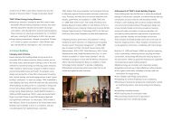
As part of our expansion plan, we held a ground breaking ceremony on July 16, <strong>20</strong>10 in Taichung’s Central Taiwan Science Park for Fab<br />
<strong>15</strong>, which will be our third Gigafab TM , or fab <strong>with</strong> capacity of more than 100,000 12-inch wafers per month when fully ramp up.<br />
Fab <strong>15</strong> will be our next “green fab” following Fab 12 and Fab 14, incorporating green concepts in energy conservation and pollution<br />
control in its design, including a process water conservation rate of 85%, reclamation of rainwater, recirculation and reuse of general exhaust<br />
heat, and development of solar power generation and LED lighting applications.<br />
Semiconductor Manufacturing Capacity and Technology<br />
We manufacture semiconductors on silicon wafers based on proprietary circuitry designs provided by our customers or third party<br />
designers. Two key factors that characterize a foundry’s manufacturing capabilities are output capacity and fabrication process technologies.<br />
Since our establishment, we have possessed the largest capacity among the world’s dedicated foundries. We also believe that we are the<br />
technology leader among the dedicated foundries in terms of our net sales of advanced semiconductors <strong>with</strong> a resolution of 65-nanometer and<br />
below, and are one of the leaders in the semiconductor manufacturing industry generally. We are the first semiconductor foundry <strong>with</strong> proven<br />
low-k interconnect technology in commercial production from the 0.13 micron node down to 40-nanometer node. Following our commercial<br />
production based on 65-nanometer Nexsys ® process technology in <strong>20</strong>06, we also unveiled 55-nanometer Nexsys ® process technology in <strong>20</strong>07.<br />
Our 65-nanometer and 55-nanometer Nexsys ® technologies are the third-generation proprietary processes that employ low-k dielectrics. In<br />
<strong>20</strong>08, we also qualified our 45-nanometer and 40-nanometer process technologies <strong>with</strong> ultra low-k dielectrics and advanced immersion<br />
lithography. We have commenced high volume production for 40-nanometer products in <strong>20</strong>10.<br />
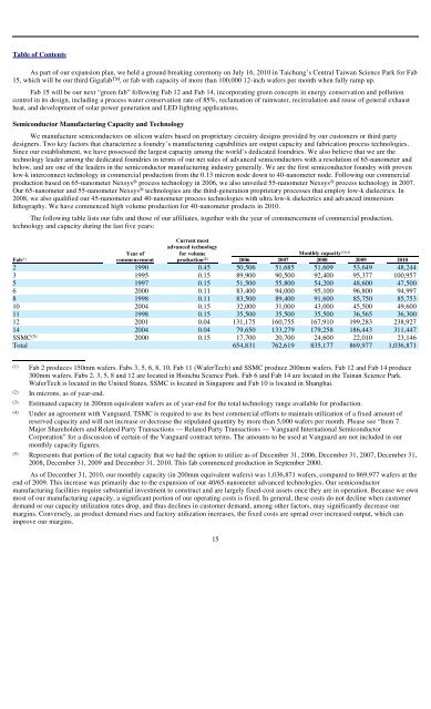
The following table lists our fabs and those of our affiliates, together <strong>with</strong> the year of commencement of commercial production,<br />
technology and capacity during the last five years:<br />
Current most<br />
advanced technology<br />
Year of for volume Monthly capacity (3)(4)<br />
Fab (1) commencement production (2) <strong>20</strong>06 <strong>20</strong>07 <strong>20</strong>08 <strong>20</strong>09 <strong>20</strong>10<br />
2 1990 0.45 50,506 51,685 51,609 53,649 48,244<br />
3 1995 0.<strong>15</strong> 89,900 90,500 92,400 95,377 100,957<br />
5 1997 0.<strong>15</strong> 51,500 55,800 54,<strong>20</strong>0 48,600 47,500<br />
6 <strong>20</strong>00 0.11 83,400 94,000 95,100 96,800 94,997<br />
8 1998 0.11 83,500 89,400 91,600 85,750 85,753<br />
10 <strong>20</strong>04 0.<strong>15</strong> 32,000 31,000 43,000 45,500 49,600<br />
11 1998 0.<strong>15</strong> 35,500 35,500 35,500 36,565 36,300<br />
12 <strong>20</strong>01 0.04 131,175 160,755 167,910 199,283 238,927<br />
14 <strong>20</strong>04 0.04 79,650 133,279 179,258 186,443 311,447<br />
SSMC (5) <strong>20</strong>00 0.<strong>15</strong> 17,700 <strong>20</strong>,700 24,600 22,010 23,146<br />
Total 654,831 762,619 835,177 869,977 1,036,871<br />
(1) Fab 2 produces <strong>15</strong>0mm wafers. Fabs 3, 5, 6, 8, 10, Fab 11 (WaferTech) and SSMC produce <strong>20</strong>0mm wafers. Fab 12 and Fab 14 produce<br />
300mm wafers. Fabs 2, 3, 5, 8 and 12 are located in Hsinchu Science Park. Fab 6 and Fab 14 are located in the Tainan Science Park.<br />
WaferTech is located in the United States, SSMC is located in Singapore and Fab 10 is located in Shanghai.<br />
(2) In microns, as of year-end.<br />
(3) Estimated capacity in <strong>20</strong>0mm equivalent wafers as of year-end for the total technology range available for production.<br />
(4) Under an agreement <strong>with</strong> Vanguard, <strong>TSMC</strong> is required to use its best commercial efforts to maintain utilization of a fixed amount of<br />
reserved capacity and will not increase or decrease the stipulated quantity by more than 5,000 wafers per month. Please see “Item 7.<br />
Major Shareholders and Related Party Transactions — Related Party Transactions — Vanguard International Semiconductor<br />
Corporation” for a discussion of certain of the Vanguard contract terms. The amounts to be used at Vanguard are not included in our<br />
monthly capacity figures.<br />
(5) Represents that portion of the total capacity that we had the option to utilize as of December 31, <strong>20</strong>06, December 31, <strong>20</strong>07, December 31,<br />
<strong>20</strong>08, December 31, <strong>20</strong>09 and December 31, <strong>20</strong>10. This fab commenced production in September <strong>20</strong>00.<br />
As of December 31, <strong>20</strong>10, our monthly capacity (in <strong>20</strong>0mm equivalent wafers) was 1,036,871 wafers, compared to 869,977 wafers at the<br />
end of <strong>20</strong>09. This increase was primarily due to the expansion of our 40/65-nanometer advanced technologies. Our semiconductor<br />
manufacturing facilities require substantial investment to construct and are largely fixed-cost assets once they are in operation. Because we own<br />
most of our manufacturing capacity, a significant portion of our operating costs is fixed. In general, these costs do not decline when customer<br />
demand or our capacity utilization rates drop, and thus declines in customer demand, among other factors, may significantly decrease our<br />
margins. Conversely, as product demand rises and factory utilization increases, the fixed costs are spread over increased output, which can<br />
improve our margins.<br />
<strong>15</strong>