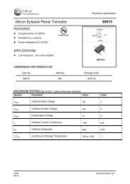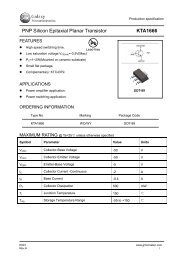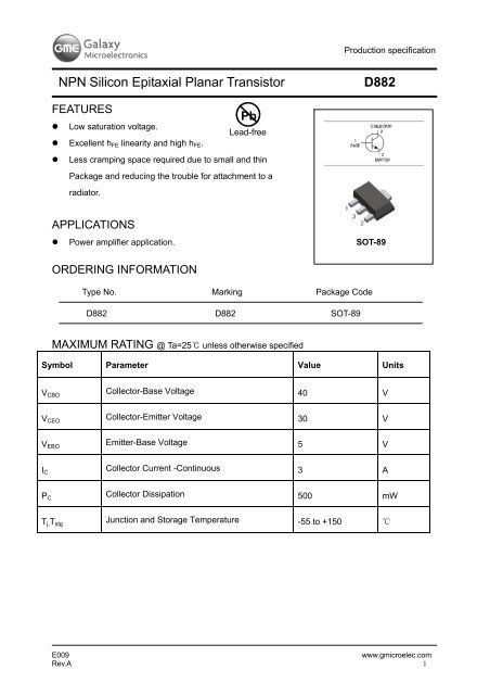
NPN Silicon Epitaxial Planar Transistor D882
NPN Silicon Epitaxial Planar Transistor D882
NPN Silicon Epitaxial Planar Transistor D882
- No tags were found...

You also want an ePaper? Increase the reach of your titles
YUMPU automatically turns print PDFs into web optimized ePapers that Google loves.
Production specification<br />
<strong>NPN</strong> <strong>Silicon</strong> <strong>Epitaxial</strong> <strong>Planar</strong> <strong>Transistor</strong><br />
<strong>D882</strong><br />
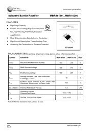
FEATURES<br />
• Low saturation voltage.<br />
• Excellent h FE linearity and high h FE .<br />
Pb<br />
Lead-free<br />
• Less cramping space required due to small and thin<br />
Package and reducing the trouble for attachment to a<br />
radiator.<br />
APPLICATIONS<br />
• Power amplifier application. SOT-89<br />
ORDERING INFORMATION<br />
Type No. Marking Package Code<br />
<strong>D882</strong> <strong>D882</strong> SOT-89<br />
MAXIMUM RATING @ Ta=25℃ unless otherwise specified<br />
Symbol Parameter Value Units<br />
V CBO<br />
Collector-Base Voltage 40 V<br />
V CEO<br />
Collector-Emitter Voltage 30 V<br />
V EBO<br />
Emitter-Base Voltage 5 V<br />
I C<br />
Collector Current -Continuous 3 A<br />
P C<br />
Collector Dissipation 500 mW<br />
T j, T stg<br />
Junction and Storage Temperature -55 to +150 ℃<br />
E009<br />
www.gmicroelec.com<br />
Rev.A 1
Production specification<br />
<strong>NPN</strong> <strong>Silicon</strong> <strong>Epitaxial</strong> <strong>Planar</strong> <strong>Transistor</strong><br />
<strong>D882</strong><br />
ELECTRICAL CHARACTERISTICS @ Ta=25℃ unless otherwise specified<br />
Parameter Symbol Test conditions MIN TYP MAX UNIT<br />
Collector-base breakdown voltage V (BR)CBO I C =100μA,I E =0 40 V<br />
Collector-emitter breakdown voltage V (BR)CEO I C =10mA,I B =0 30 V<br />
Emitter-base breakdown voltage V (BR)EBO I E =100μA,I C =0 6 V<br />
Collector cut-off current I CBO V CB =40V,I E =0 1 μA<br />
Collector cut-off current I CEO V CE =30V,I B =0 1 μA<br />
Emitter cut-off current I EBO V EB =3V,I C =0 1 μA<br />
V CE =2V,I C =20mA<br />
DC current gain h FE<br />
V CE =2V,I C =1A<br />
30<br />
60<br />
150<br />
160 400<br />
Collector-emitter saturation voltage V CE(sat)<br />
I C =2A, I B = 0.2A 0.3 0.5 V<br />
Base-emitter saturation voltage V BE(sat)<br />
I C =2A, I B =0.2A 1.0 2.0 V<br />
Transition frequency f T<br />
V CE =5V, I C = 0.1A 90 MHz<br />
Collector output capacitance C ob<br />
V CB =10V,I E =0,f=1MHz 45 pF<br />
CLASSIFICATION OF h FE<br />
Rank R Q P E<br />
Range 60-120 100-200 160-320 200-400<br />
E009<br />
www.gmicroelec.com<br />
Rev.A 2
Production specification<br />
<strong>NPN</strong> <strong>Silicon</strong> <strong>Epitaxial</strong> <strong>Planar</strong> <strong>Transistor</strong><br />
<strong>D882</strong><br />
TYPICAL CHARACTERISTICS @ Ta=25℃ unless otherwise specified<br />
E009<br />
www.gmicroelec.com<br />
Rev.A 3
Production specification<br />
<strong>NPN</strong> <strong>Silicon</strong> <strong>Epitaxial</strong> <strong>Planar</strong> <strong>Transistor</strong><br />
PACKAGE OUTLINE<br />
Plastic surface mounted package<br />
<strong>D882</strong><br />
SOT-89<br />
A<br />
H<br />
C<br />
SOT-89<br />
Dim Min Max<br />
A 4.30 4.70<br />
B 2.25 2.65<br />
K<br />
B<br />
C<br />
D<br />
1.50 Typical<br />
0.40 Typical<br />
E<br />
D<br />
L<br />
E 1.40 1.60<br />
F 0.48 Typical<br />
H 1.60 1.80<br />
J<br />
0.40 Typical<br />
L 0.90 1.10<br />
F<br />
J<br />
K 3.95 4.35<br />
All Dimensions in mm<br />
SOLDERING FOOTPRINT<br />
45°<br />
45°<br />
1.50<br />
0.90<br />
2.20<br />
0.90<br />
1.00 1.00<br />
1.50 1.50<br />
Unit:mm<br />
PACKAGE INFORMATION<br />
Device Package Shipping<br />
<strong>D882</strong> SOT-89 1000/Tape&Reel<br />
E009<br />
www.gmicroelec.com<br />
Rev.A 4