Intel - Bitsavers
Intel - Bitsavers
Intel - Bitsavers

Create successful ePaper yourself
Turn your PDF publications into a flip-book with our unique Google optimized e-Paper software.
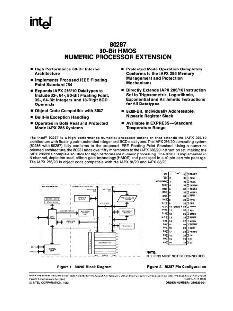
intel~<br />
80287<br />
80-Bit HMOS<br />
NUMERIC PROCESSOR EXTENSION<br />
• High Performance 80-Bit Internal<br />
Architecture<br />
• Implements Proposed IEEE Floating<br />
Point Standard 754<br />
• Expands iAPX 286/10 Datatypes to<br />
Include 32-, 64-, 80-Bit Floating Point,<br />
32-, 64-Bit Integers and 18-niqit BCD<br />
Operands<br />
• Object Code Compatible with 8087<br />
• Built-in Exception Handling<br />
• Operates in Both Real and Protected<br />
Mode iAPX 286 Systems<br />
• Protected Mode Operation Completely<br />
Conforms to the iAPX 286 Memory<br />
Management and Protection<br />
Mechanisms<br />
• Directly Extends iAPX 286/10 Instruction<br />
Set to Trigonometric, Logarithmic,<br />
Exponential and Arithmetic Instructions<br />
for All Datatypes<br />
• 8x80-Bit, Individually Addressable,<br />
Numeric Register Stack<br />
• Available in EXPRESS-Standard<br />
Temperature Range<br />
rhe <strong>Intel</strong>® 80287 is a high performance numerics processor extension that extends the iAPX 286/10<br />
architecture with floating point, extended integer and BCD data types. The iAPX 286/20 computing system<br />
(80286 with 80287) fully conforms to the proposed IEEE Floating Point Standard. Using a numerics<br />
oriented architecture, the 80287 adds over fifty mnemonics to the iAPX 286/20 instruction set, making the<br />
iAPX 286/20 a complete solution for high performance numeric processing. The 80287 is implemented in<br />
N-channel, depletion load, silicon gate technology (HMOS) and packaged in a 40-pin ceramic package.<br />
The iAPX 286/20 is object code compatible with the iAPX 86/20 and iAPX 88/20.<br />
t:==::=:=j,,,<br />
NOTE:<br />
___ L ____ -.'-_ ~,,~ _-,-- ____ ..J N.C. PINS MUST NOT BE CONNECTED.<br />
51<br />
So<br />
Vee<br />
Vss<br />
D10<br />
N.C.<br />
D9<br />
D8<br />
D7<br />
D8<br />
D5<br />
D4<br />
D3<br />
READY<br />
CKM<br />
HLDA<br />
CLK286<br />
PEACK<br />
RESET<br />
NPS1<br />
NPS2<br />
CLK<br />
CMD1<br />
Vss<br />
CMoo<br />
NPWR<br />
NPRD<br />
ERROR<br />
BUSY<br />
PEREQ<br />
DO<br />
Figure 1. 80287 Block Diagram<br />
Figure 2. 80287 Pin Configuration<br />
<strong>Intel</strong> Corporation Assumes No Responsibility for the Use of AnyCircuitry Other Than Circuitry Embodied in an <strong>Intel</strong> Product. No Other Circuit<br />
Patent Licenses are Implied. FEBRUARY 1983<br />
© INTEL CORPORATION. 1983. ORDER NUMBER: 210920·001
80287<br />
Table 1. 80287 Pin Description<br />
Symbols Type Name and Function<br />
ClK I Clock input: this clock provides the basic timing for internal 80287 operations.<br />
Special MaS level inputs are required. The 82284 or 8284A ClK<br />
outputs are compatible to this input.<br />
CKM I Clock Mode signal: indicates whether ClK input is to be divided by 3 or<br />
used directly. A HIGH input will select the latter option. This input may be<br />
connected to Vee or Vss as appropriate. This input must be either HIGH or<br />
lOW 20 ClK cycles before RESET goes lOW<br />
RESET I System Reset: causes the 80287 to immediately terminate its present activity<br />
and enter a dormant state. RESET is required to be HIGH for more than<br />
480287 ClK cycles. For proper initialization the HIGH-lOW transition must<br />
occur no sooner than 50 iJ-s after Vee and ClK meet their D.C. and A.C.<br />
specifications.<br />
015-00 I/O Data: 16-bit bidirectional data bus. Inputs to these pins may be applied<br />
asynchronous to the 80287 clock.<br />
BUSY a Busy status: asserted by the 80287 to indicate that it is currently executing<br />
a command.<br />
ERROR a Error status: reflects the ES bit of the status word. This signal indicates<br />
that an unmasked error condition exists.<br />
PEREa a Processor Extension Data Channel operand transfer request: a HIGH on<br />
this output indicates that the 80287 is ready to transfer data. PEREa will be<br />
disabled upon assertion of PEACK or upon actual data transfer, whichever<br />
occurs first, if no more transfers are required.<br />
PEACK I Processor Extension Data Channel operand transfer ACKnowledge: acknowledges<br />
that the request signal (PEREa) has been recognized. Will<br />
cause the request (PEREa) to be withdrawn in case there are no more<br />
transfers required. PEACK may be asynchronous to the 80287 clock.<br />
NPRD I Numeric Processor Read: Enables transfer of data from the 80287. l'his<br />
input may be asynchronous to the 80287 clock.<br />
NPWR I Numeric Processor Write: Enables transfer of data to the 80287. This input<br />
may be asynchronous to the 80287 clock.<br />
NPS1, NPS2 I Numeric Processor Selects: indicate the CPU is performing an ESCAPE<br />
instruction. Concurrent assertion of these signals (I.e., NPS1 is lOW and<br />
NPS2 is HIGH) enables the 80287 to perform floating point instructions. No<br />
data transfers involving the 80287 will occur unless the device is selected.<br />
These inputs may be asynchronous to the 80287 clock.<br />
CMD1, CMDO I Command lines: These, along with select inputs, allow the CPU to direct the<br />
operation of the 80287. No actions will occur if these Signals are both HIGH.<br />
These inputs may be asynchronous to the 80287 clock.<br />
2 210920-001
inter 80287<br />
Table 1. 80287 Pin Description (cont.)<br />
Symbols Type Name and Function<br />
ClK286 I CPU Clock: This input provides a sampling edge for the80287 inputs S1, SO,<br />
COD/INTA, READY, and HlDA. It must be connected to the 80286 ClK input.<br />
S1, SO __ I Status: These inputs allow the 80287 to monitor the execution of ESCAPE<br />
COD/INTA<br />
instructions by the 80286. They must be connected to the corresponding<br />
80286 pins.<br />
HlDA I Hold Acknowledge: This input informs the 80287 when the 80286 controls<br />
the local bus. It must be connected to the 80286 HlDA output.<br />
READY I Ready: The end of a bus cycle is signaled by this iriput. It must be connected<br />
to the 80286 READY input.<br />
VSS I System ground, both pins must be connected to ground.<br />
Vee I +5V supply<br />
FUNCTIONAL DESCRIPTION<br />
The 80287 Numeric Processor Extension (NPX)<br />
provides arithmetic instructions for a variety of<br />
numeric data types in iAPX 286/20 systems. It also<br />
executes numerous built-in transcendental functions<br />
(e.g., tangent and log functions). The 80287<br />
executes instructions in parallel with a 80286. It<br />
effectively extends the register and instruction set<br />
of an iAPX 286/10 system for existing iAPX 286<br />
data types and adds several new data types as well.<br />
Figure 3 presents the program visible register<br />
model of the iAPX 286/20. Essentially, the 80287<br />
can be treated as an additional resource or an<br />
extension to the iAPX 286/10 that can be used as a<br />
single unified system, the iAPX 286/20.<br />
80286<br />
15 FILE: o I 79 78<br />
AX I R1 SIGN EXPONENT<br />
BX<br />
CX<br />
DX<br />
Sl<br />
DI<br />
BP<br />
SP<br />
15<br />
I<br />
IP<br />
FLAGS<br />
~I<br />
I<br />
15<br />
I<br />
R2<br />
I R3<br />
I R4<br />
I R5<br />
I R6<br />
I R7<br />
I R8<br />
I<br />
L __ ,<br />
o I<br />
I :<br />
L ____ -,<br />
0 I<br />
I<br />
I<br />
I<br />
80287<br />
STACK:<br />
64 63<br />
SIGNIFICAND<br />
15<br />
CONTROL REGISTER<br />
STATUS REGISTER<br />
TAG WORD<br />
f- INSTRUCTION POINTER_<br />
t- DATA POINTER -<br />
Figure 3. iAPX 286/20 Architecture<br />
TAG FIELD<br />
0 1 0<br />
3<br />
210920-001
inter 80287<br />
The 80287 has two operating modes similar to the<br />
two modes of the 80286. When reset, 80287 is in<br />
the real address mode. It can be placed in the<br />
protected virtual address mode by executing the<br />
SETPM ESC instruction. The 80287 cannot be<br />
switched back to the real address mode except by<br />
reset. In the real address mode, the iAPX 286/20 is<br />
completely software compatible with iAPX 86/20,<br />
88/20.<br />
Once in protected mode, all references to memory<br />
for numerics data or status information, obey the<br />
iAPX 286 memory management and protection<br />
rules giving a fully protected extension of the<br />
80286 CPU. In the protected mode, iAPX 286/20<br />
numerics software is also completely compatible<br />
with iAPX 86/20 and iAPX 88/20.<br />
SYSTEM CONFIGURATION<br />
As a processor extension to an 80286, the 80287<br />
can be connected to the CPU as shown in Figure 4.<br />
Tbe data channel control signals (PEREa,<br />
PEACK), the BUSY signal and the NPRD, NPWR<br />
signals, allow the NPX to receive instructions and<br />
data from the CPU. When in the protected mode, all<br />
information received by the NPX is validated by the<br />
80286 memory management and protection unit.<br />
Once started, the 80287 can process in parallel<br />
with and independent of the host CPU. When the<br />
NPX detects an error or exception, it will indicate<br />
this to the CPU by asserting the ERROR signal.<br />
The NPX uses the processor extension request and<br />
acknowledge pins of the 80286 CPU to implement<br />
data transfers with memory under the protection<br />
model of the CPU. The full virtual and physical<br />
address space of the 80286 is available. Data for<br />
the 80287 in memory is addressed and represented<br />
in the same manner as for an 8087.<br />
The 80287 can operate either directly from the CPU<br />
clock or with a dedicated clock. For operation with<br />
the CPU clock (CKM=O), the 80287 works at onethird<br />
the frequency of the system clock (i.e., for an<br />
8 MHz 80286, the 16 MHz system clock is divided<br />
down to 5.3 MHz). The 80287 provides a capability<br />
to internally divide the CPU clock by three to produce<br />
the required internal clock (33% duty cycle).<br />
To use a higher performance 80287 (8 MHz), an<br />
8284A clock driver and appropriate crystal may be<br />
used to directly drive the 80287 with a 1/3 duty<br />
cycle clock on the ClK input (CKM=1).<br />
HARDWARE INTERFACE<br />
Communication of instructions and data operands<br />
between the 80286 and 80287 is handled by the<br />
CMDO, CMD1, NPS1, NPS2, NPRD, and NPWR signals.<br />
I/O port addresses 00F8H, OOFAH, and OOFCH<br />
are used by the 80286 for this communication.<br />
When any of these addresses are used, the NPS1<br />
input must be lOW and NPS2 input HIGH. The<br />
10RC and 10WC outputs of the 82288 identify I/O<br />
space transfers (see Figure 4). CMDO should be<br />
connected to latched 80286 A1 and CMD1 should<br />
be connected to latched 80286 A2.<br />
I/O ports 00F8H to OOFFH are reserved for the<br />
80286/80287 interface. To guarantee correct operation<br />
of the 80287, programs must not perform any<br />
I/O operations to these ports.<br />
The PEREa, PEACK, BUSY, and ERROR signals of<br />
the 80287 are connected to the same-named 80286<br />
input. The data pins of the 80287 should be directly<br />
connected to the 80286 data bus. Note that all bus<br />
drivers connected to the 80286 local bus must be<br />
inhibited when the 80286 reads from the 80287.<br />
The use of COD/INTA and M/IO in the decoder<br />
prevents INTA bus cycles from disabling the data<br />
transceivers.<br />
The S1, SO COD/INTA, READY, HlDA, and ClK pins<br />
of the 80286 are connected to the same named<br />
pins on the 80287. These signals allow the 80287 to<br />
monitor the execution of ESCAPE instructions by<br />
the 80826.<br />
PROGRAMMING INTERFACE<br />
Table 2 lists the seven data types the 80287 supports<br />
and presents the format for each type. These<br />
values are stored in memory with the least significant<br />
digits at the lowest memory address. Programs<br />
retrieve these values by generating the<br />
lowest address. All values should start at even<br />
addresses for maximum system performance.<br />
Internally the 80287 holds all numbers in the temporary<br />
real format. load instructions automatically<br />
convert operands represented in memory as<br />
16-, 32-, or 64-bit integers, 32- or 64-bit floating<br />
point number or 18-digit packed BCD numbers<br />
into temporary real format. Store instructions perform<br />
the reverse type conversion.<br />
4<br />
210920-001
80287<br />
RESET 1----,<br />
READY 1------,<br />
82284 ClK r----<br />
51f--<br />
SOf-<br />
82288<br />
---__j RESET<br />
READY I-~-+++---~ READY<br />
ClK<br />
ClK<br />
S11--t-'iH-1-t----I 51<br />
SO 1--1-+1-+---~ So<br />
M/iQ 1--~-+1-f-I1---I MIlO<br />
I<br />
A'5-Ao<br />
80286<br />
D'5-DO f---<br />
- ERROR PEREa f--<br />
- BUSY PEACK I--<br />
COD/iNTA HlDA<br />
DENI-~-+1-+--+1---+---+-~-+~<br />
-ii<br />
A2 A1 AD E1 I<br />
E2 8205<br />
E3 0,<br />
-I<br />
ADDRESS<br />
DT/RI-~-+1-+--+1---+---+-~-+~<br />
'---+-I~ READY<br />
0----+-1-1 ClK286<br />
'---t---+-+-I S1<br />
'---+----+-1-150 80287<br />
'-----+---+-+--1 NPRD<br />
AlEI--~-+1-t--+1---+---+-~-+1<br />
IORC<br />
COD/INTA HlDA<br />
'--+-1-1 RESET PEACK-<br />
PEREa-<br />
D'5-DO<br />
-<br />
NPS2 -Vee<br />
DATA<br />
- J D D D<br />
I-t-I~-----j(~ a a<br />
'--------f----f-t-;NPWR NPS11----------~<br />
r- ERROR CMD11------------J<br />
~ BUSY CMDOI------------~<br />
ClK CKM<br />
r;<br />
:286<br />
OR<br />
8287<br />
'--<br />
Figure 4. iAPX 286/20 System Configuration<br />
5<br />
210920·001
80287<br />
Data<br />
Range<br />
Table 2. 80287 Datatype Representation in Memory<br />
Most Significant Byte<br />
Precision<br />
Formats<br />
7 017 017 017 017 017 017 017 017 017 01<br />
Word Integer 10 4 16 Bits 115 10 I Two's Complement<br />
Short Integer 10 9 32 Bits 131 10 J Two's Complement<br />
Long Integer 10 19 64 Bits 163<br />
I 1 Two's<br />
o Complement<br />
Packed BCD 10 18 18 Digits 5 1 -I 017 0161 101 Dol<br />
Short Real 1o±38 24 Bits SlE7 Eol F1 F231 Fo Implicit<br />
Long Real 10±308 53 Bits s1<br />
E10 Eo J F1 F52 I Fo Implicit<br />
Temporary Real 1o±4932 64 Bits 5 I E14 Eo I Fo<br />
F631<br />
NOTES:<br />
(1) Integer: I s<br />
(2) Packed BCD (- 1) (017 ... 00)<br />
(3) Real: (- 1 )s(2E-BIAS){Fo Fl ... J<br />
(4) Bias =127 for Short Real<br />
1023 for Lon g Real<br />
16383 for Temp Real<br />
80287 computations use the processor's register<br />
stack. These eight 80-bit registers provide the<br />
equivalent capacity of 40 16-bit registers. The<br />
80287 register set can be accessed as a stack, with<br />
instructions operating on the top one or two stack<br />
elements, or as a fixed register set, with instructions<br />
operating on explicitly designated registers.<br />
Table 6 lists the 80287's instructions by class. No<br />
special programming tools are necessary to use<br />
the 80287 since all new instructions and data types<br />
are directly supported by the iAPX 286 assembler<br />
and appropriate high level languages. All iAPX<br />
86/88 development tools which support the 8087<br />
can also be used to develop software for the iAPX<br />
286/20 in real address mode. .<br />
Table 3 gives the execution times of some typical<br />
numeric instructions.<br />
6<br />
210920-001
80287<br />
Table 3. Execution Time for Selected 80287 Instructions<br />
Floating Point Instruction<br />
Add/Subtract<br />
Multiply (single precision)<br />
Multiply (extended precision)<br />
Divide<br />
Compare<br />
Load (double precision)<br />
Store (double precision)<br />
Square Root<br />
Tangent<br />
Exponentiation<br />
Approximate Execution<br />
Time (JLs)<br />
80287<br />
(5 MHz Operation)<br />
14/18<br />
19<br />
27<br />
39<br />
9<br />
10<br />
21<br />
36<br />
90<br />
100<br />
SOFTWARE INTERFACE<br />
The iAPX 286/20 is programmed as a single processor.<br />
All communication between th~ 80286 and<br />
the 80287 is transparent to software. The CPU automatically<br />
controls the 80287 whenever a numeric<br />
instruction is executed. All memory addressing<br />
modes, physical memory, and virtual memory of<br />
the CPU are available for use by the NPX.<br />
Since the NPX operates in parallel with the CPU,<br />
any errors detected by the NPX may be reported<br />
after the CPU has executed the ESCAPE instruction<br />
which caused it. To allow identification of the<br />
failing numeric instruction, the NPX contains two<br />
pointer registers which identify the address of the<br />
failing numeric instruction and the numeric<br />
memory operand if appropriate for the instruction<br />
encountering this error.<br />
INTERRUPT DESCRIPTION<br />
Several interrupts of the iAPX 286 are used to<br />
report exceptional conditions while executing<br />
numeric programs in either real or protected<br />
mode. The interrupts and their functions are<br />
shown in Table 4.<br />
PROCESSOR ARCHITECTURE<br />
As shown in Figure 1, the NPX is internally divided<br />
into two processing elements, the bus interface<br />
unit (BIU) and the numeric execution unit (NEU).<br />
The NEU executes all numeric instructions, while<br />
the BIU receives and decodes instructions, requests<br />
operand transfers to and from memory and<br />
executes processor control instructions. The two<br />
units are able to operate independently of one<br />
another allowing the BIU to maintain asynchronous<br />
communication with the CPU while the NEU<br />
is busy processing a numeric instruction.<br />
BUS INTERFACE UNIT<br />
The BIU decodes the ESC instruction executed by<br />
the CPU. If the ESC code defines a math instruction,<br />
the BIU transmits the formatted instruction to<br />
the NEU.lf the ESC code defines an administrative<br />
instruction, the BIU executes it independently of<br />
the NEU. The parallel operation of the NPX with the<br />
CPU is normally transparant to the user. The BIU<br />
generates the BUSY and ERROR signals for<br />
80826/80287 processor synchronization.<br />
The 80287 executes a si ngle numeric instruction at<br />
a time. When executing most ESC instructions, the<br />
7<br />
210921).001
80287<br />
Table 4. Interrupt Vectors<br />
Interrupt Number<br />
Interrupt Function<br />
7 An ESC instruction was encountered when EM or TS of the 80286 MSW was set.<br />
EM=1 indicates that software emulation of the instruction is required. When TS is<br />
set, either an ESC or WAIT instruction will cause interrupt 7. This indicates that the<br />
current NPX context may not belong to the current task.<br />
9 The second or subsequent words of a numeric operand in memory exceeded a<br />
segment's limit. This interrupt occurs after executing an ESC instruction. The saved<br />
return address will not point at the numeric instruction causing this interrupt. After<br />
processing the addressing error, the iAPX 286 program can be restarted at the<br />
return address with IRET. The address of the failing numeric instruction and<br />
numeric operand are saved in the 80287. An interrupt handler for this interrupt must<br />
execute FNINIT before any other ESC or WAIT instruction.<br />
13 The starting address of a numeric operand is not in the segment's limit. The return<br />
address will point at the ESC instruction (including prefixes) causing this error. The<br />
80287 has not executed this instruction. The instruction and data address in 80287<br />
refer to a previous, correctly executed, instruction.<br />
16 The previous numeric instruction caused an unmasked numeric error. The address<br />
of the faulty numeric instruction or numeric data operand is stored in the 80287.<br />
Only ESC or WAIT instructions can cause this interrupt. The 80286 return address<br />
will point at a WAIT or ESC instruction, including prefixes, which may be restarted<br />
after clearing the error condition in the NPX.<br />
80286 tests the BUSYpin and waits until the 80287<br />
indicates that it is not busy before initiating the<br />
command. Once initiated, the 80286 continues<br />
program execution while the 80287 executes the<br />
ESC instruction. In iAPX 86/20 systems, this<br />
synchronization is achieved by placing a WAIT instruction<br />
before an ESC instruction. For most ESC<br />
instructions, the iAPX 286/20 does not require a<br />
WAIT instruction before the ESC opcode. However,<br />
the iAPX 286/20 will operate correctly with these<br />
WAIT instructions. In all cases, a WAIT or ESC instruction<br />
should be inserted after any 80287 store<br />
to memory (except FSTSW and FSTCW) or load<br />
from memory (except FLDENVor FRSTOR) before<br />
the 80286 reads or changes the value.<br />
Data transfers between memory and the 80287,<br />
when needed, are controlled by the PEREQ<br />
PEACK, NPRD, NPWR, NPS1, NPS2 signals. The<br />
80286 does the actual data transfer with memory<br />
through its processor extension data channel.<br />
Numeric data transfers with memory performed by<br />
the 80286 use the same timing as any other bus<br />
cycle. Control signals for the 80287 are generated<br />
by the 80826 as shown in Figure 4, and meet the<br />
timing requirements shown in the AC requirements<br />
section.<br />
NUMERIC EXECUTION UNIT<br />
The NEU executes all instructions that involve the<br />
register stack; these include arithmetic, logical,<br />
transcendental, constant and data transfer instructions.<br />
The data path in the NEU is 84 bits wide<br />
(68 fraction bits, 15 exponent bits and a sign bit)<br />
which allows internal operand transfers to be performed<br />
at very high speeds.<br />
When the NEU begins executing an instruction, it<br />
activates the BIU BUSY signal. This signal is used<br />
in conjunction with the CPU WAIT instruction or<br />
automatically with most of the ESC instructions to<br />
synchronize both processors.<br />
REGISTER SET<br />
The 80287 register set is shown in Figure 5. Each of<br />
the eight data registers in the 8087's register stack<br />
8<br />
210920-001
80287<br />
DATA FIELD<br />
TAG FIELD<br />
~~79~T7_B ______ ~G4-r6~3 ________ ~ __ ~ ____ ~0 1<br />
SIGN EXPONENT SIGNIFICAND<br />
15<br />
CONTROL REGISTER<br />
STATUS REGISTER<br />
TAG WORD<br />
- INSTRUCTION POINTER -<br />
- DATAPOINTER -<br />
Figure 5. 80287 Register Set<br />
is 80 bits wide and is divided into "fields" corresponding<br />
to the NPX's temporary real data type.<br />
At a given point in time the TOP field in the status<br />
word identifies the cu rrent top-of-stack reg ister. A<br />
"push" operation decrements TOP by 1 and loads a<br />
value into the new top register. A "pop" operation<br />
stores the value from the current top register and<br />
then increments TOP by 1. Like 80286 stacks in<br />
memory, the 80287 register stack grows "down"<br />
toward lower-addressed registers.<br />
Instructions may address the data registers either<br />
implicitly or explicitly. Many instructions operate<br />
on the register at the top of the stack. These instructions<br />
implicitly address the register pointed<br />
by the TOP. Other instructions allow the programmer<br />
to explicitly specify the register which is to be<br />
used. Explicit register addressing is "top-relative."<br />
STATUS WORD<br />
The 16-bit status word (in the status register)<br />
shown in Figure 6 reflects the overall state of the<br />
80287. It may be read and inspected by CPU code.<br />
The busy bit (bit 15) indicates whether the NEU is<br />
executing an instruction (B = 1) or is idle (B = 0).<br />
The instructions FSTSW, FSTENV, and FSAVE<br />
which store the status word are executed exclusively<br />
by the BIU and do not set the busy bit<br />
themselves or require the Busy bit be cleared in<br />
order to be executed.<br />
The four numeric condition code bits (Co-Ca) are<br />
similar to the flags in a CPU: instructions that perform<br />
arithmetic operations update these bits to<br />
reflect the outcome of NDP operations. The effect<br />
of these instructions on the condition code bits is<br />
summarized in Tables Sa and 5b.<br />
Bits 14-12 of the status word point to the 80287<br />
register that is the current top-of-stack (TOP) as<br />
described above. Figure 6 shows the six error flags<br />
in bits 7-0 of the status word. The section on ex·<br />
ception handling explains how they are set and<br />
used.<br />
Bit 7 is the error status bit. This bit is set if any<br />
unmasked exception bit is set and cleared otherwise.<br />
If this bit is set, the ERROR signal is asserted.<br />
Bits 5-0 are set to indicate that the NEU has<br />
detected an exception while executing an<br />
instruction.<br />
9<br />
210920-001
80287<br />
15 o<br />
I B IC:JI TOplc.IC, ICoIESI x IPEIUEloEIZEIDEllEI<br />
I<br />
g:ES IS SET IF ANY UNMASKED EXCEPTION BIT IS SET, CLEARED OTHERWISE.<br />
(3)~6~ ~~~b~~ FOR CONDITION CODE INTERPRETATION.<br />
.<br />
000 ~ Register 0 is Top of Stack<br />
001 ~ Register 1 is Top of Stack<br />
111 ~ Register 7 is Top of Stack<br />
EXCE PTION FLAGS (1 ~ EXCEPTION HAS OCCURRED)<br />
INVALID OPERATION"<br />
DENORMALIZED OPERAND'<br />
ZERO DIVIDE'<br />
OVERFLOW'<br />
UNDERFLOW'<br />
PRECISION"<br />
(RESE RVED)<br />
ERRO R STATUSI1I<br />
COND ITION CODE (2 )<br />
TOP OF STACK POINTER13I<br />
NEU BUSY<br />
'For definitions, see the section on exception handling<br />
Figure 6. 80287 Status Word<br />
TAG WORD<br />
The tag word marks the content of each register as<br />
shown in Figure 7. The principal function of the tag<br />
word is to optimize the NPX's performance. The<br />
tag word can be used, however, to interpret the<br />
contents of 80287 registers.<br />
INSTRUCTION AND DATA POINTERS<br />
The instruction and data pointers (See Figures 8a<br />
and 8b) are provided for user-written error handlers.<br />
Whenever the 80287 executes a new instruction,<br />
the BIU saves the instruction address, the<br />
operand address (if present) and the instruction<br />
opcode. 80287 instructions can store this data into<br />
memory.<br />
The instruction and data pointers appear in one of<br />
two formats depending on the operating mode of<br />
the 80287. In real mode, these values are the 20-bit<br />
physical address and 11-bit opcode formatted like<br />
the 8087. In protected mode, these values are the<br />
32-bit virtual addresses used by the program<br />
which executed an ESC instruction. The same<br />
FLDENV/FSTENV/FSAVE/FRSTOR instructions as<br />
those of the 8087 are used to transfer these values<br />
between the 80287 registers and memory.<br />
The saved instruction address in the 80287 will<br />
point at any prefixes which preceded the instruction.<br />
This is different than in the 8087 which only<br />
pointed at the ESCAPE instruction opcode.<br />
CONTROL WORD<br />
The NPX provides several processing options<br />
which are selected by loading a word from memory<br />
into the control word. Figure 9 shows the format<br />
and encoding of fields in the control word.<br />
The low order byte of this control word configures<br />
the 80287 error and exception maski ng. Bits 5-0 of<br />
the control word contain individual masks for each<br />
of the six exceptions that the 80287 recognizes.<br />
The high order byte of the control word configures<br />
the 80287 operating mode including precision,<br />
10<br />
210920-001
inter 80287<br />
Table Sa. Condition Code Interpretation<br />
Instruction<br />
Type<br />
Ca<br />
C2<br />
C1<br />
Co<br />
Interpretation<br />
Compare, Test 0 0<br />
0 0<br />
1 0<br />
1 1<br />
Remainder 01 0<br />
U 1<br />
Examine 0 0<br />
0 0<br />
0 0<br />
0 0<br />
0 1<br />
0 1<br />
0 1<br />
0 1<br />
1 0<br />
1 0<br />
1 0<br />
1 0<br />
1 1<br />
1 1<br />
1 1<br />
1 1<br />
NOTES:<br />
1. ST = Top of stack<br />
2. X = value is not affected by instruction<br />
3. U = value is undefined following instruction<br />
4. Qn = Quotient bit n<br />
X<br />
X<br />
X<br />
X<br />
00<br />
U<br />
0<br />
0<br />
1<br />
1<br />
0<br />
0<br />
1<br />
1<br />
0<br />
0<br />
1<br />
1<br />
0<br />
0<br />
1<br />
1<br />
0 ST> Source or 0 (FTST)<br />
1 ST < Source or 0 (FTST)<br />
a ST = Source or a (FTST)<br />
1 ST is not comparable<br />
02 Complete reduction with<br />
three low bits of quotient<br />
(See Table 5b)<br />
U Incomplete Reduction<br />
0 Valid, positive unnormalized<br />
1 Invalid, positive, exponent =0<br />
0 Valid, negative, unnormalized<br />
1 Invalid, negative, exponent =0<br />
0 Valid, positive, normalized<br />
1 Infinity, positive<br />
0 Valid, negative, normalized<br />
1 Infinity, negative<br />
0 Zero, positive<br />
1 Empty<br />
0 Zero, negative<br />
1 Empty<br />
0 Invalid, positive, exponent = 0<br />
1 Empty<br />
0 Invalid, negative, exponent = 0<br />
1 Empty<br />
Table 5b. Condition Code Interpretation after<br />
FPREM Instruction As a Function of<br />
Dividend Value<br />
Dividend Range Q2 Q1 Qo<br />
Dividend < 2 • Modulus Cs C1 00<br />
Dividend < 4 • Modulus Cs 01 00<br />
Dividend;. 4 • Modulus 02 01 00<br />
NOTE:<br />
1. Previous valueof indicated bit. not affected by FPREM<br />
instruction execution.<br />
rounding, and infinity control. The precision control<br />
bits (bits 9-8) can be used to set the 80287<br />
internal operating precision at less than the<br />
default of temporary real (80-bit) precision. This<br />
can be useful in providing compatibility with the<br />
early generation arithmetic processors of smaller<br />
precision than the 80287. The rounding control<br />
bits (bits 11-10) provide for directed rounding and<br />
true chop as well as the unbiased round to nearest<br />
even mode specified in the IEEE standard. Control<br />
over closure of the number space at infinity is also<br />
provided (either affine closure: ± 00, or projective<br />
closure: 00, is treated as unsigned, may be<br />
specified).<br />
11<br />
210920·001
inter 80287<br />
TAG VALUES:<br />
00 ~ VALID<br />
01 ~ ZERO<br />
10 ~ INVALID or INFINITY<br />
11 ~ EMPTY<br />
Figure 7. 80287 Tag Word<br />
15<br />
MEMORY OFFSET<br />
CONTROL WORD +0<br />
STATUS WORD +2<br />
TAG WORD +4<br />
IP OFFSET +6<br />
CS SELECTOR +8<br />
DATA OPERAND OFFSET +10<br />
DATA OPERAND SELECTOR +12<br />
Figure 8a. Protected Mode Instruction and Data Pointer Image in Memory<br />
EXCEPTION HANDLING<br />
The 80287 detects six different exception conditions<br />
that can occur during instruction execution.<br />
Any or all exceptions will cause the assertion of<br />
ERROR signal if the appropriate exception masks<br />
are not set.<br />
The exceptions that the 80287 detects and the<br />
'default' procedures that will be carried out if the<br />
exception is masked, are as follows:<br />
Invalid Operation: Stack overflow, stack under·<br />
flow, indeterminate form (0/0, 00-00, etc.) or the use<br />
of a Non-Number (NAN) as an operand. An exponent<br />
value of all ones and non-zero significand<br />
is reserved to identify NANs. If this exception is<br />
masked, the 80287 default response is to generate<br />
a specific NAN called INDEFINITE, or to propagate<br />
already existing NANs as the calculation result.<br />
Overflow: The result is too large in magnitude to<br />
fit the specified format. The 80287 will generate an<br />
encoding for infinity if this exception is masked.<br />
Zero Divisor: The divisor is zero while the dividend<br />
is a non-infinite, non-zero number. Again, the<br />
80287 will generate an encoding for infinity if this<br />
exception is masked.<br />
Underflow: The result is non-zero but too small in<br />
magnitude to fit in the specified format. If this<br />
exception is masked the 82087 Will denormalize<br />
(shift right) the fraction until the exponent is in<br />
range. The process is called gradual underflow.<br />
12<br />
210920-001
inter 80287<br />
15<br />
MEMORY<br />
OFFSET<br />
CONTROL WORD<br />
+0<br />
STATUS WORD<br />
TAG WORD<br />
INSTRUCTION POINTER (15-0)<br />
INSTRUCTION )1 I INSTRUCTION<br />
POINTER (19-16) 0 OPCODE (10-0)<br />
+2<br />
+4<br />
+6<br />
+8<br />
DATA POINTER (15-0)<br />
+10<br />
DATA POINTER I<br />
(19-16)<br />
15 1211<br />
0<br />
+12<br />
Figure 8b. Real Mode 80287 Instruction and Data Pointer Image in Memory<br />
16<br />
I x x X IIC I RC I PC I x I x IPMluMloMlzMIDMllMI<br />
(1) PRECISION CONTROL<br />
00 ~ 24 BITS<br />
01 = RESERVED<br />
10 ~ 53 BITS<br />
11 ~ 64 BITS<br />
/1<br />
(2)ROUNDING CONTROL<br />
00 ~ ROUND TO NEAREST OR EVEN<br />
01 = ROUND DOWN (TOWARD -x)<br />
10 ~ ROUND UP (TOWARD +x)<br />
11 ~ CHOP (TRUNCATE TOWARD ZERO)<br />
EXCEPTION MASKS (l~EXCEPTION IS MASKED)<br />
INVALID OPERATION<br />
DENORMALIZED OPERAND<br />
ZERO DIVIDE<br />
OVERFLOW<br />
UNDERFLOW<br />
PRECISION<br />
(RESERVED)<br />
(RESERVED)<br />
PRECISION CONTROL (1)<br />
ROUNDING CONTROL(2)<br />
INFINITY CONTROL (0 ~ PROJECTIVE, 1 ~ AFFINE)<br />
(RESERVED)<br />
Figure 9. 80287 Control Word<br />
13 210920-001
80287<br />
Denormalized Operand: At least one of the<br />
operands is denormalized; it has the smallest exponent<br />
but a non-zero significand. Normal processing<br />
continues if this exception is masked off.<br />
Inexact Result: If the true result is not exactly<br />
representable in the specified format, the result is<br />
rounded according to the rounding mode, and this<br />
flag is set. If this exception is masked, processing<br />
will simply continue.<br />
If the error is not masked, the corresponding error<br />
bit and the error status bit (ES) in the control word<br />
will be set, and the ERROR output signal will be<br />
asserted. If the CPU attempts to execute another<br />
ESC or WAIT instruction, exception 7 will occur.<br />
The error condition must be resolved via an interrupt<br />
service routine. The 80287 saves the address<br />
of the floating point instruction causing the error<br />
as well as the address of the lowest memory location<br />
of any memory operand required by that<br />
instruction.<br />
iAPX 86/20 COMPATIBILITY:<br />
iAPX 286/20 supports portability of iAPX 86/20<br />
programs when it is in the real address mode.<br />
However, because of differences in the numeric<br />
error handing techniques, error handling routines<br />
may need to be changed. The differences between<br />
an iAPX 286/20 and iAPX 86/20 are:<br />
1. The NPX error signal does not pass through an<br />
interrupt controller (8087 INT signal does).<br />
Therefore, any interrupt controller oriented instructions<br />
for the iAPX 86/20 may have to be<br />
deleted.<br />
2. Interrupt vector 16 must point at the numeric<br />
error handler routine.<br />
3. The saved floating point instruction address in<br />
the 80287 includes any leading prefixes before<br />
the ESCAPE opcode. The corresponding saved<br />
address of the 8087 does not include leading<br />
prefixes.<br />
4. In protected mode, the format of the saved instruction<br />
and operand pointers is different than<br />
for the 8087. The instruction opcode is not<br />
saved-it must be read from memory if needed.<br />
5. Interrupt 7 will occur when executing ESC instructions<br />
with eitherTS or EM of MSW=1. IfTS<br />
of MSW=1 then WAIT will also cause interrupt<br />
7. An interrupt handler should be added to handle<br />
this situation.<br />
6. Interrupt 9 will occur if the second or subsequent<br />
words of a floating point operand fall<br />
outside a segment's size. Interrupt 13 will occur<br />
if the starting address of a numeric operand<br />
falls outside a segment's size. An interrupt<br />
handler should be added to report these programming<br />
errors.<br />
In the protected mode, iAPX 86/20 application<br />
code can be directly ported via recompilation if the<br />
'286 memory protection rules are not violated.<br />
14<br />
210920-001
80287<br />
ABSOLUTE MAXIMUM RATINGS*<br />
Ambient Temperature Under Bias .. O°C to 70°C<br />
Storage Temperature ........ -65°C to +150°C<br />
Voltage on Any Pin with<br />
Respect to Ground ............... -1.0 to +7V<br />
Power Dissipation .................... 3.0 Watt<br />
'NOTICE: Stresses above those listed under Absolute<br />
Maximum Ratings may cause permanent<br />
damage to the device. This is a stress rating only<br />
and functional operation of the device at these or<br />
any other conditions above those indicated in the<br />
operational sections of this specification is not<br />
implied. Exposure to absolute maximum rating<br />
conditions for extended periods may affect device<br />
reliability.<br />
D.C. CHARACTERISTICS TA = ooe to 70 0 e, Vcc = 5V ± 10%<br />
Symbol Parameter Min. Max. Units Test Conditions<br />
Vil Input low Voltage -0.5 +0.8 V<br />
VIH Input High Voltage 2.0 Vcc+0.5 V<br />
VOL Output low Voltage 0.45 V 10l = 3.0 mA<br />
VOH Output High Voltage 2.4 V 10H = .400 p.A<br />
Icc Power Supply Current 475 mA TA = 25°C<br />
III Input leakage Current ±10 p.A OV
80287<br />
A.C. CHARACTERISTICS TA=O°C to 70°C, VCC= 5V± 10%<br />
TIMING REQUIREMENTS<br />
Symbol Parameter Min.<br />
Test<br />
Max. Units Conditions<br />
TClCl<br />
ClK cycle period<br />
CKM=1 : 5MHz 200<br />
8M Hz 125<br />
CKM=O: 16MHz 62.5<br />
ns<br />
500<br />
500 at 1.5 V<br />
250<br />
TClCH ClK low time CKM=1 118<br />
CKM=O 15<br />
TCHCl ClK high time CKM=1 69<br />
CKM=O 20<br />
TCH1CH2<br />
ClK rise time<br />
ns at 0.6 V<br />
230 at 0.8 V<br />
ns at 3.8 V<br />
235 at 2.0 V<br />
10 ns from 1.0 to 3.5 V<br />
TCl2Cl1<br />
ClK fall time<br />
10 ns from 3.5 to 1.0V<br />
TDVWH Data valid set up to NPWR inactive 75<br />
TWHDX Data hold from NPWR inactive 0<br />
ns<br />
ns<br />
TWlWH,<br />
TRlRH<br />
NPWR, NPRD active time<br />
95<br />
ns<br />
TAVRl,<br />
TAVWl<br />
Command Valid to NPWR or NPRD<br />
active<br />
0<br />
ns<br />
at 1.5 V<br />
TMHRl<br />
Minimum response from PEREQ active<br />
set up to NPRD active<br />
130<br />
,<br />
ns<br />
TKlKH PEACK active time 95<br />
TKHKl PEACK inactive time 95<br />
TKHCH PEACK inactive to NPWR, NPRD 0<br />
inactive<br />
ns<br />
ns<br />
ns<br />
TCHKl<br />
Data Channel NPRD, NPWR inactive<br />
set up to PEACK active<br />
-25<br />
ns<br />
TWHAX, Command hold from NPWR, NPRD 0<br />
TRHAX inactive<br />
ns<br />
TKlCl<br />
PEACK active set up to command<br />
active<br />
0<br />
ns<br />
T2ClCl 80286 Clock period 62.5<br />
T2ClCH 80286 Clock low time 15<br />
T2CHCl 80286 Clock high time 20<br />
250 ns<br />
230 ns at 0.8V<br />
235 ns at 2.0V<br />
16<br />
21092()'001
inter 80287<br />
A.C. CHARACTERISTICS TA=O°C to 70°C, VCC= 5V± 10%<br />
TIMING REQUIREMENTS (cont.)<br />
Symbol Parameter Min.<br />
Max.<br />
Units<br />
Test<br />
Conditions<br />
TCLSH S1, SO hold time 0<br />
ns<br />
TSVCL S1, SO valid setup time 22.5<br />
ns<br />
TCIVCL COD/INTA valid setup time 0<br />
ns<br />
TCLCIH COD/INTA hold time 0<br />
TRVCL READY valid setup time 38.5<br />
ns<br />
ns<br />
at 1.5 V<br />
TCLRH READY hold time 25<br />
ns<br />
THVCL HLDA valid setup time 0<br />
ns<br />
TCLHH HLDA hold time 0<br />
ns<br />
TCLIH Input from CLK hold time 45<br />
TIVCH Input to CLK setup time 70<br />
NOTE:<br />
1. To guarantee a predetermined response for testing purposes.<br />
ns<br />
at 1.5V<br />
ns (See Note 1)<br />
A.C. CHARACTERISTICS-TIMING RESPONSES<br />
Symbol Parameter Min.<br />
Max.<br />
Units<br />
Test<br />
Conditions<br />
TRHQZ<br />
TRLQV<br />
NPRD inactive to data tri-state<br />
NPRD active to data valid<br />
37.5 ns CL=20pF-100pF<br />
at 1.5V<br />
60 ns<br />
TILBH ERROR active to BUSY inactive 100<br />
TWLBV<br />
TCLML<br />
TKLML<br />
NPWR active to BUSY valid<br />
NPRD, NPWR active to PEREQ<br />
inactive<br />
PEACK active to PEREQ inactive<br />
ns<br />
100 ns<br />
120 ns<br />
127 ns<br />
CL=100pF at 1.5V<br />
CL = 100pF at 1.SV<br />
(See Note 1)<br />
TCMDI<br />
Minimum command inactive time<br />
Write-Write 95<br />
Read-Read 150<br />
Write-Read 105<br />
Read-Write 95<br />
ns<br />
ns at 1.5V<br />
ns<br />
ns<br />
TRHQH Data valid hold from NPRD inactive 5<br />
ns CL=40pF at 1.5V<br />
NOTE:<br />
1. On last data transfer of numeric instruction.<br />
17<br />
21092()'001
80287<br />
WAVEFORMS<br />
CLOCK TIMING<br />
RESET<br />
NOTE:<br />
1. Shown for CKM=1, when CKM=O TIVCH is measured from the second falling edge of ClK. These inputs<br />
may be asynchronous to ClK. This input timing guarantees a predetermined response.<br />
18 2109211-001
inter<br />
80287<br />
WAVEFORMS (cont.)<br />
DATA TRANSFER TIMING<br />
CMDO CMD1<br />
iiiPSi,NPS2<br />
,<br />
VALID<br />
W<br />
_TRLRH_<br />
TRHAX<br />
TAVRL ..; r-<br />
-TRLQV t--<br />
/I///V<br />
VALID<br />
\\\\\\<br />
TAVWL<br />
TWLWH- II<br />
DATA OUT<br />
TWHAX<br />
I""<br />
TRANSFER<br />
FRDM<br />
80287<br />
~ ....<br />
\ 7<br />
TDVWH<br />
TWHDX<br />
BUSY<br />
.... TWLBV<br />
DATA MAY CHANGE<br />
\ DATA IN \f DATA MAY CHANGE<br />
J\ VALID J<br />
DATA<br />
~b=<br />
--/fc--<br />
TRANSFER<br />
TO<br />
DATA CHANNEL TIMING<br />
_M~~~<br />
NI':S1,NPS2<br />
~<br />
TAVWL<br />
TAVRL<br />
VALID<br />
""'l<br />
_TRHQZ~<br />
"'-TRHQH-<br />
TRHAX't<br />
TWHAX /~<br />
".., ~_T_M_:K-R:-C-L----4--------------M~----------~------------+------<br />
~--------TKLKH--------~<br />
19 21Q920-001
80287<br />
WAVEFORMS (cont.)<br />
ERROR OUTPUT TIMING<br />
J<br />
BUSY _j--'~<br />
~oo, l' 1<br />
80286 STATUS TIMING<br />
'---T2CLCL---o~TS<br />
CLK286<br />
COD/INTA<br />
HLDA<br />
NOTES:<br />
1. This input transition occurs before Ts.<br />
2. This input transition occurs after Te.<br />
20 210920-001
80287<br />
Table 6. 80287 Extensions to the 80286 Instruction Set<br />
Data Transfer<br />
I Optional<br />
8,16 BII<br />
Displacement<br />
Clock Count Range<br />
32 Bit 32 Bit 64 Bit 16 Bit<br />
Real Integer Real Integer<br />
FLO ~ LOAD<br />
1 MF<br />
00 01 10 11<br />
IntegerlReal Memory to ST(O)<br />
1 ESCAPE MF 1 1<br />
38-56 52-60 40-60 46-54<br />
long Integer Memory to ST(O)<br />
[ ESCAPE 1 1 1 [<br />
MOD<br />
1 a 1 RIM [==gl~P=J<br />
60-68<br />
Temporary Real Memory to<br />
ST(O)<br />
BCD Memory to ST(O)<br />
ST(i) to ST(O)<br />
[ ESCAPE a 1 1 [ MOD<br />
I ESCAPE 1 1 1 I MOD<br />
I ESCAPE<br />
a a 1 I 1 1 a a a ST(i) 1<br />
1 a 1 RIM [==gl~P==:<br />
_._._._._.-<br />
1 a a RIM 1_ _ _ ':H~P _ J<br />
53-65<br />
290-310<br />
17-22<br />
F5T ~ STORE<br />
ST(O) to IntegerlReal Memory<br />
ST(O) to ST(i)<br />
F5TP ~ STORE AND POP<br />
ST(O) to IntegerlReal Memory<br />
ST(O) to long Integer Memory<br />
ST(O) to Temporary Real<br />
Memory<br />
ST(O) to BCD Memory<br />
I ESCAPE MF 1 1 MOD a 1 a RIM 1- = = ~I~P = :<br />
I ESCAPE 1 a 1 I 1 1 a 1 a ST(i) I<br />
'E-S-C-A-P-E--M-F--1--rI-M-O-D--0-1-1-R-I-M'[ ~ ~ jl~P ~ J<br />
ESCAPE 1 1 1 I MOD 1 1 1 RIM [==~i~= :<br />
ESCAPE a 1 1 I MOD 1 1 1 RIM [=~~I~P~J<br />
ESCAPE 1 1 1 1 MOD 1 1 a RIM [~~'~I~~:<br />
84-90 82-92 96-104 80-90<br />
15-22<br />
86-92 84-94 98-106 82-92<br />
94-105<br />
52-58<br />
520-540<br />
ST(O) to 5T(i)<br />
ESCAPE 1 a 1 I 1 1 a 1 1 ST(i) 1<br />
17-24<br />
FXCH ~ Exchange ST(i) and<br />
ST(O)<br />
ESCAPE a a 1 1 1 1 a a 1 ST(i) 1<br />
10-15<br />
Comparison<br />
FCOM ~ Compare<br />
IntegerlReal Memory to ST(O)<br />
ST(i) to ST (0)<br />
1 ESCAPE MF a 1 MOD a 1 a RIM [~~I~~J<br />
I ESCAPE a a a I 1 1 a 1 a ST(i) I<br />
60-70 78-91 65-75 72-86<br />
40-50<br />
FCOMP ~ Compare and Pop<br />
IntegerlReal Memory to ST(O)<br />
ST(i) to ST(O)<br />
FCOMPP ~ Compare ST(1) to<br />
ST(O) and Pop Twice<br />
FTST ~ Test ST(O)<br />
FXAM ~ Examine ST(O)<br />
Mnemonics © <strong>Intel</strong> 1982.<br />
[ESCAPE MF a [ MOD a 1 1 RIM [jl~P=J<br />
1 ESCAPE a a a [ 1 1 a 1 1 ST(i)<br />
I ESCAPE 1 1 a I 1 1 a 1 1 a a 1<br />
I ESCAPE a a 1 I 1 1 1 a a 1 a a<br />
[ ESCAPE a a 1 [ 1 1 1 a a 1 a 1<br />
63-73 80-93 67-77 74-88<br />
45-52<br />
45-55<br />
38-48<br />
12-23<br />
21<br />
210920-001
80287<br />
Table 6. 80287 Extensions to the 80286 Instruction Set (cont.)<br />
I Optional<br />
Clock Count Range<br />
8,16 Bit 32 Bit 32 Bit 64 Bit 16 Bit<br />
Constants Displacement Real Integer Real Integer<br />
I MF<br />
~<br />
00 01 10 11<br />
FLoZ ~ LOAD + 0.0 into ST(O)<br />
I ESCAPE 0 0 I I I I I 0 I I I 0 I<br />
11-17<br />
FLol ~ LOAD + 1.0 into ST(O)<br />
I ESCAPE 0 0 I I I I I 0 I 0 0 0 I<br />
15-21<br />
FLoPI ~ LOAD 7r into ST(O)<br />
I ESCAPE 0 0 I I I I I 0 I 0 I I<br />
I<br />
16-22<br />
FLoL2l ~ LOAD log2 10 into<br />
I ESCAPE 0 0 I I I I I 0 1 0- 0 I I<br />
16-22<br />
ST(O)<br />
FLoL2E ~ LOAD log2 e into<br />
I ESCAPE 0 0 1 I I 1 1 0 I 0 I 0 I<br />
15-21<br />
ST(O)<br />
FLoLG2 ~ LOAD 10g,O 2 into<br />
ST(O)<br />
1 ESCAPE 0 0 I 1 I 1 I 0 I I 0 0 1<br />
18-24<br />
FLoLN2 ~ LOAD loge2 into<br />
I ESCAPE 0 0 I I I I I 0 I I 0 I 1<br />
ST(O)<br />
17-23<br />
Arithmetic<br />
FAoo ~ Addition<br />
-.-.- -,<br />
Integer/Real Memory with ST(O) ESCAPE MF 0 MOD 0 0 0 R/M DISP i 90-120 108-143 95-125 102-137<br />
I I<br />
1-<br />
ST(i) and Sl(O)<br />
1 ESCAPE d P 0 1 I I 0 0 0 ST(i) 70-100 (Note 1)<br />
1<br />
FSUB = Subtraction<br />
I I [ _.-.- -,<br />
Integer/Real Memory with ST(O) ESCAPE MF 0 MOD 1 0 R RIM DISP 90-120 108-143 95-125 102-137<br />
_._.-<br />
-'<br />
ST(i) and Sl(O)<br />
I ESCAPE d P 0 I I I I 0 R R/M I<br />
70-100 (Note I)<br />
FMUL = Multiplication<br />
Integer/Real Memory with ST(O)<br />
_. _. -.-<br />
_.-.-<br />
,<br />
1 ESCAPE MF 0 I MOD 0 0 I R/M [ -. DISP -.- ..!<br />
110-125 130-144 112-168 124-138<br />
ST(i) and ST(O)<br />
I ESCAPE d P 0 I I 1 0 0 I R/M I<br />
90-145 (Note I)<br />
FDIV = Division - _. -.-<br />
Integer/Real Memory with ST(O)<br />
_. _. _.- ..!<br />
1 ESCAPE MF 0 1 MOD I I R R/M I DISP -,<br />
215-225 230-243 220-230 224-238<br />
ST(i) and ST(O)<br />
1 ESCAPE d P 0 1 I 1 1 I R RIM 193-203 (Note I)<br />
I<br />
FSQRl ~ Square Root of ST(O)<br />
I ESCAPE 0 0 I I I I I I I 0 I 0 I<br />
180-186<br />
FSCALE ~ Scale Sl(O) by ST(1) 1<br />
ESCAPE 0 0 I<br />
I 1 I I I I I 0 I I<br />
32-38<br />
FPREM = Partial Remainder of ESCAPE 0 0 1<br />
1<br />
ST(O) +ST(I)-<br />
1 I I I I 1 0 0 0 1<br />
15-190<br />
FRNoINl ~ Round ST(O) to<br />
I ESCAPE 0 0 I I I I I I I I 0 0 I<br />
16-50<br />
Integer<br />
NOTE:<br />
1. If P=1 then add 5 clocks.<br />
22 21092()"OOl
inter 80287<br />
Table 6. 80287 Extensions to the 80286 Instruction Set (cont.)<br />
Optional<br />
8,16 Bit<br />
Displacement<br />
Clock Count Range<br />
FXTRACT ~ Extract<br />
Components of StIO)<br />
FABS = Absolute Value of<br />
STIO)<br />
FCHS ~ Change Sign of STIO)<br />
ESCAPE 0 0 1 I 1 1 1 1 0 1 0 0<br />
ESCAPE 11<br />
ESCAPE 0 o<br />
27-55<br />
10-17<br />
10-17<br />
Transcendental<br />
FPTAN = Partial Tangent of<br />
STIO)<br />
FPATAN = Partial Arctangent<br />
of STIO) +STll)<br />
F2XMl ~ 2ST(O)_1<br />
ESCAPE 0 0 1 1 1 1 1 0 0 1 0<br />
ESCAPE<br />
ESCAPE 0<br />
o<br />
30-540<br />
250-800<br />
310-630<br />
FYL2X ~ STll)' L092<br />
[STIO)l<br />
FYL2XPl ~ ST(l)' Log2<br />
[ST(O) +1[<br />
ESCAPE<br />
ESCAPE<br />
o<br />
o<br />
900-1100<br />
700-1000<br />
Processor Control<br />
FINIT = Initialize NPX<br />
ESCAPE<br />
2-8<br />
FSETPM ~ Enter Protected<br />
Mode<br />
FSTSW AX ~ Store Control<br />
Word<br />
FLDCW ~ Load Control Word<br />
FSTCW = Store Control Word<br />
FSTSW = Store Status Word<br />
ESCAPE<br />
ESCAPE<br />
o<br />
o I<br />
L-__________ ESCAPE 0 0 L-____________ MOD<br />
~<br />
RIM<br />
I_._.~.I~~_J<br />
LE_S_C_A_P_E __ O __.LM_O_D_____<br />
R_/M ___ I ~~~I~~~J<br />
LE_S_C_A_P_E ____.LM_O_D_____<br />
R_/M __....JI ~~~I~~~J<br />
2-8<br />
10-16<br />
7-14<br />
12-18<br />
12-18<br />
FCLEX = Clear Exceptions<br />
FSTENV = Store Environment<br />
FLDENV = Load Environment<br />
FSAVE ~ Save State<br />
FRSTOR ~ Restore State<br />
ESCAPE 1 1 010<br />
,------------,------------------, _._._.-.-.-.-<br />
'---E_S_C_A_P_E__ O __ l--L_M_O_D _____ R_/M __....JI __ ~~~_J<br />
L-__________ ESCAPE 0 L-____________ MOD RIM<br />
~<br />
I __ ~I~~._J<br />
ESCAPE MOD RIM -Disp--'<br />
._._._._._.J<br />
L-E_S_C_A_P_E __ 0 __ L-M_O_D __ 0 ___ R_/M __--'I_=9~~=J<br />
2-8<br />
40-50<br />
35-45<br />
205-215<br />
205-215<br />
FINCSTP ~ Increment Stack<br />
Pointer<br />
ESCAPE<br />
o<br />
6-12<br />
FDECSTP ~ Decrement Stack<br />
Pointer<br />
ESCAPE 0<br />
6-12<br />
23<br />
210920-001
80287<br />
Table 6. 80287 Extensions to the 80286 Instruction Set (cont.)<br />
Clock Count Range<br />
FFREE = Free ST(i) ESCAPE 1 0 1 I 1 1 0 0 0 ST(i)<br />
FNOP = No Operation ESCAPE 0 0 1 I 1 1 0 1 0 0 0 0 I<br />
9-16<br />
10-16<br />
NOTES:<br />
1. if mod=OO then DISP=O', disp-Iow and disp-high are absent<br />
if mod=01 then DISP=disp-Iow sign-extended to 16-bits, disp-high is absent<br />
if mod=10 then DISP=disp-high; disp-Iow<br />
if mod=11 then rim is treated as an ST(i) field<br />
2. if r/m=OOO thenEA=(BX) + (SI) +DISP<br />
if r/m=001 then EA=(BX) + (DI) +DISP<br />
if r/m=010 then EA=(BP) + (SI) H)ISP<br />
if r/m=Oll then EA=(BP) + (DI) +DISP<br />
if r/m=100 then EA=(SI) + DISP<br />
if r/m=101 then EA=(DI) + DISP<br />
if r/m=110 then EA=(BP) + DISP<br />
if r/m=111 then EA=(BX) + DISP<br />
'except if mod=OOO and r/m=110 then EA =disp-high; disp-Iow.<br />
3. MF= Memory Format<br />
00-32-bit Real<br />
01-32-bit Integer<br />
10-64-bit Real<br />
11-16-bit Integer<br />
4. ST(O) = Current stack top<br />
ST(il ith register below stack top<br />
5. d = Desti nation<br />
O-Destination is ST(O)<br />
1-Destination is ST(i)<br />
6. P= Pop<br />
O-No pop<br />
1-Pop ST(O)<br />
7. R= Reverse: When d=1 reverse the sense of R<br />
O-Destination (op) Source<br />
1-Source (op) Destination<br />
8. For FSQRT: -0 .. ST(O) .. +00<br />
For FSCALE: _2 15 .. ST(1) < +2 15 and ST(1) integer<br />
For F2XM1: 0 .. ST(O)" 2- 1<br />
For FYL2X: 0 < ST(O)