Displaytech Ltd - CompArt International
Displaytech Ltd - CompArt International
Displaytech Ltd - CompArt International

You also want an ePaper? Increase the reach of your titles
YUMPU automatically turns print PDFs into web optimized ePapers that Google loves.
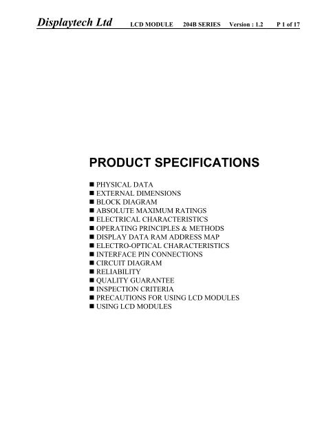
<strong>Displaytech</strong> <strong>Ltd</strong> LCD MODULE 204B SERIES Version : 1.2 P 1 of 17<br />
PRODUCT SPECIFICATIONS<br />
• PHYSICAL DATA<br />
• EXTERNAL DIMENSIONS<br />
• BLOCK DIAGRAM<br />
• ABSOLUTE MAXIMUM RATINGS<br />
• ELECTRICAL CHARACTERISTICS<br />
• OPERATING PRINCIPLES & METHODS<br />
• DISPLAY DATA RAM ADDRESS MAP<br />
• ELECTRO-OPTICAL CHARACTERISTICS<br />
• INTERFACE PIN CONNECTIONS<br />
• CIRCUIT DIAGRAM<br />
• RELIABILITY<br />
• QUALITY GUARANTEE<br />
• INSPECTION CRITERIA<br />
• PRECAUTIONS FOR USING LCD MODULES<br />
• USING LCD MODULES
<strong>Displaytech</strong> <strong>Ltd</strong> LCD MODULE 204B SERIES Version : 1.2 P 2 of 17<br />
• PHYSICAL DATA<br />
Item Contents Unit<br />
LCD type TN / STN / FSTN ---<br />
LCD duty 1/16 ---<br />
LCD bias 1/5 ---<br />
Viewing direction 6 / 12 o’clock<br />
Module size (W×H×T) 98 × 60 × 11.0 MAX (14.0 MAX W/LED BACKLIGHT) mm<br />
Viewing area (W×H) 76 × 25.2 mm<br />
Number of characters (characters×lines) 20 × 4 ---<br />
Character matrix (W×H) 5 × 8 dots<br />
Character size (W×H) 2.95 × 4.75 mm<br />
Dot size (W×H) 0.55 × 0.55 mm<br />
Dot pitch (W×H) 0.60 × 0.60 mm<br />
• EXTERNAL DIMENSIONS<br />
• BLOCK DIAGRAM
<strong>Displaytech</strong> <strong>Ltd</strong> LCD MODULE 204B SERIES Version : 1.2 P 3 of 17<br />
• ABSOLUTE MAXIMUM RATINGS ( Ta = 25°C )<br />
Parameter Symbol Min Max Unit<br />
Supply voltage for logic VDD -0.3 7.0 V<br />
Supply voltage for LCD VDD - VO -0.3 VDD+0.3 V<br />
Input voltage VI -0.3 VDD+0.3 V<br />
Normal operating temperature TOP 0 50 °C<br />
Normal storage temperature TST -10 60 °C<br />
Wide operating / storage TOP / TST -30 80 °C<br />
temperature (except FSTN)<br />
Wide operating / storage<br />
temperature (FSTN)<br />
TOP / TST -30 70 °C<br />
• ELECTRICAL CHARACTERISTICS ( VDD = +5V±10% , VSS = 0V, Ta = 25°C )<br />
DC Characteristics<br />
Parameter Symbol Condition Min Typ Max Unit<br />
Supply voltage for logic VDD --- 4.5 5.0 5.5 V<br />
Supply current for logic IDD --- --- 1.44 4 mA<br />
Operating voltage for LCD VDD - VO 25°C 4.5 4.8 5.1 V<br />
Input voltage ' H ' level VIH --- VDD - 2.2 --- VDD V<br />
Input voltage ' L ' level VIL --- 0 --- 0.8 V<br />
• Backlight operating information (Ta = 25°C )<br />
Supply voltage VF (V)<br />
Supply current IF (mA)<br />
LED Backlight Min Typ Max Min Typ Max<br />
Light box Y/G (-2) --- 4.2 4.6 --- 280 480<br />
EL Enable voltage EON (VAC)<br />
EL frequency LF (Hz)<br />
EL Backlight Min Typ Max Min Typ Max<br />
EL (B) --- 100 150 --- 400 1000<br />
AC Characteristics<br />
• Write mode<br />
Characteristic Symbol Min. Typ. Max. Unit Test pin<br />
E cycle time t C 500 --- --- ns E<br />
E rise time t r --- --- 25 ns E<br />
E fall time t f --- --- 25 ns E<br />
E pulse width (High, Low) t W 220 --- --- ns E<br />
R/W and RS set-up time t SU1 40 --- --- ns R/W, RS<br />
R/W and RS hold time t h1 10 --- --- ns R/W, RS<br />
Data set-up time t SU2 60 --- --- ns DB 0 ~ DB 7<br />
Data hold time t h2 10 --- --- ns DB 0 ~ DB 7
<strong>Displaytech</strong> <strong>Ltd</strong> LCD MODULE 204B SERIES Version : 1.2 P 4 of 17<br />
• Read mode<br />
Characteristic Symbol Min. Typ. Max. Unit Test pin<br />
E cycle time t C 500 --- --- ns E<br />
E rise time t r --- --- 25 ns E<br />
E fall time t f --- --- 25 ns E<br />
E pulse width t W 220 --- --- ns E<br />
R/W and RS set-up time t SU 40 --- --- ns R/W, RS<br />
R/W and RS hold time t h 10 --- --- ns R/W, RS<br />
Data output delay time t D --- --- 120 ns DB 0 ~ DB 7<br />
Data hold time t DH 20 --- --- ns DB 0 ~ DB 7<br />
• Interface mode with ,KS0063B<br />
Characteristic Symbol Min. Typ. Max. Unit Test pin<br />
Clock pulse width High t CWH 800 --- --- ns CLK<br />
Clock pulse width Low t CWL 800 --- --- ns CLK<br />
Data set-up time t SU 300 --- --- ns DB 0 ~ DB 7<br />
Data hold time t DH 300 --- --- ns DB 0 ~ DB 7<br />
Clock set-up time t CSU 500 --- --- ns CLK<br />
M Delay time t DM -1000 --- 1000 ns M
<strong>Displaytech</strong> <strong>Ltd</strong> LCD MODULE 204B SERIES Version : 1.2 P 5 of 17<br />
• OPERATING PRINCIPLES & METHODS<br />
Control and Display Command<br />
DB 7 DB 6 DB 5 DB 4 DB 3 DB 2 DB DB Command RS R/<br />
Time<br />
Remark<br />
Execution<br />
W<br />
1 0<br />
(f osc = 250kHz)<br />
DISPLAY L L L L L L L L L H 1.64ms<br />
CLEAR<br />
RETURN L L L L L L L L H X 1.64ms Cursor move to first digit<br />
HOME<br />
ENTRY MODE L L L L L L L H I/D SH 42µs • I/D : Set cursor move direction<br />
SET<br />
H Increase<br />
I/D<br />
L Decrease<br />
• SH : Specifies shift of display<br />
SH<br />
H<br />
L<br />
Display is shifted<br />
Display is not<br />
shifted<br />
DISPLAY<br />
ON/OFF<br />
L L L L L L H D C B 42µs • Display<br />
H<br />
D<br />
L<br />
• Cursor<br />
H<br />
C<br />
L<br />
• Blinking<br />
H<br />
B<br />
L<br />
Display on<br />
Display off<br />
Cursor on<br />
Cursor off<br />
Blinking on<br />
Blinking off<br />
SHIFT L L L L L H S/C R/L X X 42µs<br />
S/C<br />
H<br />
L<br />
Display shift<br />
Cursor move<br />
R/L<br />
H<br />
L<br />
Right shift<br />
Left shift<br />
SET<br />
FUNCTION<br />
L L L L H DL N F X X 42µs<br />
DL<br />
H<br />
L<br />
8 bits interface<br />
4 bits interface<br />
N<br />
H<br />
L<br />
2 line display<br />
1 line display<br />
F<br />
H<br />
L<br />
5 X 10 dots<br />
5 X 7 dots<br />
SET CG RAM<br />
ADDRESS<br />
SET DD RAM<br />
ADDRESS<br />
READ BUSY<br />
FLAG &<br />
ADDRESS<br />
L L L H CG RAM address<br />
(corresponds to cursor address)<br />
42µs CG RAM Data is sent and<br />
received after this setting<br />
L L H DD RAM address 42µs DD RAM Data is sent and<br />
received after this setting<br />
L H BF Address Counter used for<br />
0µs<br />
both DD & CG RAM address<br />
BF<br />
H Busy<br />
L Ready<br />
− Reads BF indication internal<br />
operating is being performed<br />
− Reads address counter contents<br />
WRITE DATA H L Write Data 46µs Write data into DD or CG RAM<br />
READ DATA H H Read Data 46µs Read data from DD or CG RAM<br />
X : Don’t care
<strong>Displaytech</strong> <strong>Ltd</strong> LCD MODULE 204B SERIES Version : 1.2 P 6 of 17<br />
Initializing by Internal Reset Circuit<br />
The KS0076B automatically initializes (resets) when the power is on using the internal reset circuit. The following<br />
instruction are executed in initialization. The busy flag is kept in busy state (BF=1) until initialization ends. The busy state<br />
is 10ms after VDD rises to 4.5V.<br />
(1) Display Clear<br />
(2) Function Set<br />
DL = 1 : 8-bit interface data<br />
N = 0 : 1-line display<br />
F = 0 : 5x7-dot character font<br />
(3) Display On/Off Control<br />
D = 0 : Display Off<br />
C = 0 : Cursor Off<br />
B = 0 : Blink Off<br />
(4) Entry Mode Set<br />
I/D = 1 : +1 (Increment)<br />
S = 0 : No Shift<br />
Initializing by Instruction<br />
Power On<br />
|<br />
Wait for more than 15ms after VDD rises to 4.5V<br />
|<br />
RS R/W DB7 DB6 DB5 DB4 DB3 DB2 DB1 DB0<br />
0 0 0 0 1 1 * * * *<br />
|<br />
Wait for more than 4.1ms<br />
|<br />
RS R/W DB7 DB6 DB5 DB4 DB3 DB2 DB1 DB0<br />
0 0 0 0 1 1 * * * *<br />
|<br />
Wait for more than 100µs<br />
|<br />
RS R/W DB7 DB6 DB5 DB4 DB3 DB2 DB1 DB0<br />
0 0 0 0 1 1 * * * *<br />
|<br />
|<br />
|<br />
|<br />
|<br />
|<br />
RS R/W DB7 DB6 DB5 DB4 DB3 DB2 DB1 DB0<br />
0 0 0 0 1 1 N F * *<br />
0 0 0 0 0 0 1 0 0 0 Display Off<br />
0 0 0 0 0 0 0 0 0 1 Display Clear<br />
0 0 0 0 0 0 0 1 I/D Entry Mode Set<br />
S<br />
|<br />
â<br />
Initialization ends<br />
BF cannot be checked before this instruction.<br />
Function Set<br />
BF cannot be checked before this instruction.<br />
Function Set<br />
BF cannot be checked before this instruction.<br />
Function Set<br />
BF can be checked after following<br />
instruction.<br />
When BF is not checked, the waiting time<br />
between instructions is longer than execution<br />
instruction time.<br />
Function Set (Specify the number of display<br />
lines and character font.) The number of<br />
display lines and character font cannot be<br />
changed afterwards.
<strong>Displaytech</strong> <strong>Ltd</strong> LCD MODULE 204B SERIES Version : 1.2 P 7 of 17<br />
Standard Character Pattern<br />
• DISPLAY DATA RAM ADDRESS MAP<br />
Characters 1 2 3 4 5 6 7 8 9 10 11 12 13 14 15 16 17 18 19 20<br />
First line (H) 00 01 02 03 04 05 06 07 08 09 0A 0B 0C 0D 0E 0F 10 11 12 13<br />
Second line (H) 40 41 42 43 44 45 46 47 48 49 4A 4B 4C 4D 4E 4F 50 51 52 53<br />
Third line (H) 14 15 16 17 18 19 1A 1B 1C 1D 1E 1F 20 21 22 23 24 25 26 27<br />
Fourth line (H) 54 55 56 57 58 59 5A 5B 5C 5D 5E 5F 60 61 62 63 64 65 66 67
<strong>Displaytech</strong> <strong>Ltd</strong> LCD MODULE 204B SERIES Version : 1.2 P 8 of 17<br />
• ELECTRO-OPTICAL CHARACTERISTICS ( VOP = 5.0V, Ta = 25°C, Transflective version)<br />
LCD mode<br />
Typ response<br />
time Tr (ms)<br />
Normal<br />
temp<br />
Wide<br />
temp<br />
Typ response<br />
time Tf (ms)<br />
Normal<br />
temp<br />
Wide<br />
temp<br />
Typ viewing angle q (deg)<br />
Typ contrast<br />
ratio Cr ˘ = 0 ˘ = 90 ˘ = 180 ˘ = 270<br />
TN (A) 28 20 40 5 40<br />
STN Y/G (B) 30 60 48 57 47<br />
STN Blue (C) 6 52 25 33 33<br />
STN Grey (D)<br />
275 147 61 57<br />
12 60 37 55 38<br />
FSTN (F) 38 65 49 58 48<br />
FSTN Negative (G)<br />
18 53 25 34 33<br />
Note1: Definition of response time.<br />
Note2: Definition of contrast ratio ‘Cr’ . Note3: Definition of viewing angle range ‘θ’.
<strong>Displaytech</strong> <strong>Ltd</strong> LCD MODULE 204B SERIES Version : 1.2 P 9 of 17<br />
• INTERFACE PIN CONNECTIONS<br />
Pin NO. Symbol Level Description<br />
1, 17 VSS 0V Ground<br />
2, 18 VDD 5.0V Supply voltage for logic<br />
3, 19 VO --- Input voltage for LCD<br />
4, 20 RS H/L H : Data signal, L : Instruction signal<br />
5, 21 R/W H/L H : Read mode, L : Write mode<br />
6, 22 E H, H → L Enable signal for KS0076<br />
7, 23 DB0 H/L Data bit 0<br />
8, 24 DB1 H/L Data bit 1<br />
9, 25 DB2 H/L Data bit 2<br />
10, 26 DB3 H/L Data bit 3<br />
11, 27 DB4 H/L Data bit 4<br />
12, 28 DB5 H/L Data bit 5<br />
13, 29 DB6 H/L Data bit 6<br />
14, 30 DB7 H/L Data bit 7<br />
15, 31 A --- Back light anode<br />
16, 32 K --- Back light cathode
<strong>Displaytech</strong> <strong>Ltd</strong> LCD MODULE 204B SERIES Version : 1.2 P 10 of 17<br />
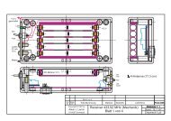
• CIRCUIT DIAGRAM
<strong>Displaytech</strong> <strong>Ltd</strong> LCD MODULE 204B SERIES Version : 1.2 P 11 of 17<br />
• RELIABILITY<br />
Content of Reliability Test<br />
Environmental Test<br />
No. Test Item Content of Test Test Condition Applicable<br />
Standard<br />
1 High temperature Endurance test applying the high storage 60 °C<br />
------<br />
storage<br />
temperature for a long time.<br />
200 hrs<br />
2 Low temperature Endurance test applying the low storage -10 °C<br />
------<br />
storage<br />
temperature for a long time.<br />
200 hrs<br />
3 High temperature<br />
operation<br />
Endurance test applying the electric stress<br />
(Voltage & Current) and the thermal stress to<br />
50 °C<br />
200 hrs ------<br />
the element for a long time.<br />
4 Low temperature Endurance test applying the electric stress 0 °C<br />
------<br />
operation<br />
under low temperature for a long time. 200 hrs<br />
5 High temperature /<br />
Humidity storage<br />
Endurance test applying the high temperature<br />
and high humidity storage for a long time.<br />
60 °C , 90 %RH<br />
96 hrs<br />
MIL-202E-103B<br />
JIS-C5023<br />
6 High temperature /<br />
Humidity operation<br />
Endurance test applying the electric stress<br />
(Voltage & Current) and temperature /<br />
humidity stress to the element for a long time.<br />
7 Temperature cycle Endurance test applying the low and high<br />
temperature cycle.<br />
25°C<br />
5min.<br />
-10°C<br />
30min<br />
.<br />
1 cycle<br />
60°C<br />
30min<br />
.<br />
40 °C , 90 %RH<br />
96 hrs<br />
-10°C / 60°C<br />
10 cycles<br />
MIL-202E-103B<br />
JIS-C5023<br />
------<br />
Mechanical Test<br />
8 Vibration test Endurance test applying the vibration during<br />
transportation and using.<br />
9 Shock test Constructional and mechanical endurance test<br />
applying the shock during transportation.<br />
10 Atmospheric<br />
pressure test<br />
Endurance test applying the atmospheric<br />
pressure during transportation by air.<br />
Others<br />
11 Static electricity test Endurance test applying the electric stress to<br />
the terminal.<br />
10∼22Hz → 1.5mmp-p<br />
22∼500Hz → 1.5G<br />
Total 0.5hrs<br />
50G half sign<br />
wave 1l msedc<br />
3 times of each<br />
direction<br />
115 mbar<br />
40 hrs<br />
VS=800V , RS=1.5 kΩ<br />
CS=100 pF<br />
1 time<br />
∗∗∗ Supply voltage for logic system = 5V. Supply voltage for LCD system = Operating voltage at 25°C.<br />
MIL-202E-201A<br />
JIS-C5025<br />
JIS-C7022-A-10<br />
MIL-202E-213B<br />
MIL-202E-105C<br />
MIL-883B-<br />
3015.1<br />
Failure Judgement Criterion<br />
Criterion Item Test Item No. Failure Judgment Criterion<br />
1 2 3 4 5 6 7 8 9 10 11<br />
Basic specification<br />
Out of the Basic Specification<br />
Electrical characteristic<br />
Out of the DC and AC Characterstic<br />
Mechanical characterstic<br />
Out of the Mechanical Specification Color<br />
change : Out of Limit Apperance Specification<br />
Optical characterstic<br />
Out of the Apperance Standard
<strong>Displaytech</strong> <strong>Ltd</strong> LCD MODULE 204B SERIES Version : 1.2 P 12 of 17<br />
• QUALITY GUARANTEE<br />
Acceptable Quality Level<br />
Each lot should satisfy the quality level defined as follows.<br />
- Inspection method : MIL-STD-105E LEVEL II Normal one time sampling<br />
- AQL<br />
Partition AQL Definition<br />
A: Major 0.4% Functional defective as product<br />
B: Minor 1.5% Satisfy all functions as product but not satisfy cosmetic standard<br />
Definition of ‘LOT’<br />
One lot means the delivery quantity to customer at one time.<br />
Conditions of Cosmetic Inspection<br />
• Environmental condition<br />
The inspection should be performed at the 1m of height from the LCD module under 2 pieces of 40W white<br />
fluorescent lamps (Normal temperature 20∼25°C and normal humidity 60±15%RH).<br />
• Inspection method<br />
The visual check should be performed vertically at more than 30cm distance from the LCD panel.<br />
• Driving voltage<br />
The VO value which the most optimal contrast can be obtained near the specified VO in the specification. (Within<br />
±0.5V of the typical value at 25°C.).<br />
• INSPECTION CRITERIA<br />
Module Cosmetic Criteria<br />
No. Item Judgement Criterion Partition<br />
1 Difference in Spec. None allowed Major<br />
2 Pattern peeling No substrate pattern peeling and floating Major<br />
3 Soldering defects No soldering missing<br />
No soldering bridge<br />
No cold soldering<br />
Major<br />
Major<br />
Minor<br />
4 Resist flaw on substrate Invisible copper foil (∅0.5mm or more) on substrate pattern Minor<br />
5 Accretion of metallic<br />
Foreign matter<br />
No soldering dust<br />
No accretion of metallic foreign matters (Not exceed ∅0.2mm)<br />
Minor<br />
Minor<br />
6 Stain No stain to spoil cosmetic badly Minor<br />
7 Plate discoloring No plate fading, rusting and discoloring Minor<br />
8 Solder amount<br />
1. Lead parts<br />
a. Soldering side of PCB<br />
Solder to form a ‘Filet’<br />
all around the lead.<br />
Solder should not hide the<br />
lead form perfectly. (too much)<br />
b. Components side<br />
( In case of ‘Through Hole PCB’ )<br />
Minor<br />
Solder to reach the Components side of PCB.<br />
2. Flat packages Either ‘toe’ (A) or ‘heal’ (B) of<br />
the lead to be covered by ‘Filet’. A<br />
B<br />
Minor<br />
Lead form to be assume over<br />
solder.<br />
3. Chips (3/2) H ≥ h ≥ (1/2) H Minor<br />
h H
<strong>Displaytech</strong> <strong>Ltd</strong> LCD MODULE 204B SERIES Version : 1.2 P 13 of 17<br />
Screen Cosmetic Criteria (Non-Operating)<br />
No. Defect Judgement Criterion Partition<br />
1 Spots In accordance with Screen Cosmetic Criteria (Operating) No.1. Minor<br />
2 Lines In accordance with Screen Cosmetic Criteria (Operating) No.2. Minor<br />
3 Bubbles in polarizer<br />
Size : d mm<br />
Acceptable Qty in active area<br />
Minor<br />
d ≤ 0.3<br />
Disregard<br />
0.3 < d ≤ 1.0 3<br />
1.0 < d ≤ 1.5 1<br />
1.5 < d 0<br />
4 Scratch In accordance with spots and lines operating cosmetic criteria. When the light Minor<br />
reflects on the panel surface, the scratches are not to be remarkable.<br />
5 Allowable density Above defects should be separated more than 30mm each other. Minor<br />
6 Coloration Not to be noticeable coloration in the viewing area of the LCD panels.<br />
Minor<br />
Back-lit type should be judged with back-lit on state only.<br />
7 Contamination Not to be noticeable. Minor<br />
Screen Cosmetic Criteria (Operating)<br />
No. Defect Judgement Criterion Partition<br />
1 Spots A) Clear<br />
Minor<br />
Size : d mm<br />
Acceptable Qty in active area<br />
d ≤ 0.1<br />
Disregard<br />
0.1 < d ≤ 0.2 6<br />
0.2 < d ≤ 0.3 2<br />
0.3 < d 0<br />
Note : Including pin holes and defective dots which must be within one pixel<br />
size.<br />
B) Unclear<br />
Size : d mm<br />
Acceptable Qty in active area<br />
d ≤ 0.2<br />
Disregard<br />
0.2 < d ≤ 0.5 6<br />
0.5 < d ≤ 0.7 2<br />
0.7 < d 0<br />
2 Lines A) Clear<br />
Minor<br />
L 5.0<br />
2.0<br />
∞<br />
(6)<br />
(0)<br />
See No. 1<br />
0.02<br />
0.05<br />
0.1<br />
W<br />
Note : ( ) - Acceptable Qty in active area<br />
L - Length (mm)<br />
W - Width (mm)<br />
∞ - Disregard<br />
B) Unclear<br />
L 10.0<br />
∞<br />
(6)<br />
(0)<br />
2.0<br />
0.05<br />
0.3<br />
0.5<br />
See No. 1<br />
W<br />
‘Clear’ = The shade and size are not changed by VO.<br />
‘Unclear’ = The shade and size are changed by VO.
<strong>Displaytech</strong> <strong>Ltd</strong> LCD MODULE 204B SERIES Version : 1.2 P 14 of 17<br />
Screen Cosmetic Criteria (Operating) (Continued)<br />
No. Defect Judgement Criterion Partition<br />
3 Rubbing line Not to be noticeable.<br />
4 Allowable density Above defects should be separated more than 10mm each other. Minor<br />
5 Rainbow Not to be noticeable. Minor<br />
6 Dot size To be 95% ∼ 105% of the dot size (Typ.) in drawing.<br />
Partial defects of each dot (ex. pin-hole) should be treated as ‘spot’.<br />
(see Screen Cosmetic Criteria (Operating) No.1)<br />
Minor<br />
7 Uneven brightness<br />
(only back-lit type<br />
module)<br />
Uneven brightness must be BMAX / BMIN ≤ 2<br />
- BMAX : Max. value by measure in 5 points<br />
- BMIN : Min. value by measure in 5 points<br />
Divide active area into 4 vertically and horizontally.<br />
Measure 5 points shown in the following figure.<br />
Minor<br />
◦ ◦<br />
◦<br />
◦ ◦<br />
◦ : Measuring points<br />
Note :<br />
(1) Size : d = (long length + short length) / 2<br />
(2) The limit samples for each item have priority.<br />
(3) Complexed defects are defined item by item, but if the number of defects are defined in above table, the total number<br />
should not exceed 10.<br />
(4) In case of ‘concentration’, even the spots or the lines of ‘disregarded’ size should not allowed. Following three<br />
situations should be treated as ‘concentration’.<br />
- 7 or over defects in circle of ∅5mm.<br />
- 10 or over defects in circle of ∅10mm.<br />
- 20 or over defects in circle of ∅20mm.<br />
• PRECAUTIONS FOR USING LCD MODULES<br />
Handing Precautions<br />
(1) The display panel is made of glass. Do not subject it to a mechanical shock by dropping it or impact.<br />
(2) If the display panel is damaged and the liquid crystal substance leaks out, be sure not to get any in your mouth. If the<br />
substance contacts your skin or clothes, wash it off using soap and water.<br />
(3) Do not apply excessive force to the display surface or the adjoining areas since this may cause the color tone to vary.<br />
(4) The polarizer covering the display surface of the LCD module is soft and easily scratched. Handle this polarizer<br />
carefully.<br />
(5) If the display surface becomes contaminated, breathe on the surface and gently wipe it with a soft dry cloth. If it is<br />
heavily contaminated, moisten cloth with one of the following solvents :<br />
- Isopropyl alcohol<br />
- Ethyl alcohol<br />
(6) Solvents other than those above-mentioned may damage the polarizer. Especially, do not use the following.<br />
- Water<br />
- Ketone<br />
- Aromatic solvents<br />
(7) Exercise care to minimize corrosion of the electrode. Corrosion of the electrodes is accelerated by water droplets,<br />
moisture condensation or a current flow in a high-humidity environment.
<strong>Displaytech</strong> <strong>Ltd</strong> LCD MODULE 204B SERIES Version : 1.2 P 15 of 17<br />
(8) Install the LCD Module by using the mounting holes. When mounting the LCD module make sure it is free of<br />
twisting, warping and distortion. In particular, do not forcibly pull or bend the I/O cable or the backlight cable.<br />
(9) Do not attempt to disassemble or process the LCD module.<br />
(10) NC terminal should be open. Do not connect anything.<br />
(11) If the logic circuit power is off, do not apply the input signals.<br />
(12) To prevent destruction of the elements by static electricity, be careful to maintain an optimum work environment.<br />
- Be sure to ground the body when handling the LCD modules.<br />
- Tools required for assembling, such as soldering irons, must be properly grounded.<br />
- To reduce the amount of static electricity generated, do not conduct assembling and other work under dry<br />
conditions.<br />
- The LCD module is coated with a film to protect the display surface. Exercise care when peeling off this protective<br />
film since static electricity may be generated.<br />
Storage Precautions<br />
When storing the LCD modules, avoid exposure to direct sunlight or to the light of fluorescent lamps. Keep the modules<br />
in bags (avoid high temperature / high humidity and low temperatures below 0°C). Whenever possible, the LCD modules<br />
should be stored in the same conditions in which they were shipped from our company.<br />
Others<br />
Liquid crystals solidify under low temperature (below the storage temperature range) leading to defective orientation or<br />
the generation of air bubbles (black or white). Air bubbles may also be generated if the module is subject to a low<br />
temperature.<br />
If the LCD modules have been operating for a long time showing the same display patterns, the display patterns may<br />
remain on the screen as ghost images and a slight contrast irregularity may also appear. A normal operating status can be<br />
regained by suspending use for some time. It should be noted that this phenomenon does not adversely affect performance<br />
reliability.<br />
To minimize the performance degradation of the LCD modules resulting from destruction caused by static electricity<br />
etc., exercise care to avoid holding the following sections when handling the modules.<br />
- Exposed area of the printed circuit board.<br />
- Terminal electrode sections.<br />
• USING LCD MODULES<br />
Liquid Crystal Display Modules<br />
LCD is composed of glass and polarizer. Pay attention to the following items when handling.<br />
(1) Please keep the temperature within specified range for use and storage. Polarization degradation, bubble generation<br />
or polarizer peel-off may occur with high temperature and high humidity.<br />
(2) Do not touch, push or rub the exposed polarizers with anything harder than an HB pencil lead (glass, tweezers, etc.).<br />
(3) N-hexane is recommended for cleaning the adhesives used to attach front/rear polarizers and reflectors made of<br />
organic substances which will be damaged by chemicals such as acetone, toluene, ethanol and isopropylalcohol.<br />
(4) When the display surface becomes dusty, wipe gently with absorbent cotton or other soft material like chamois soaked<br />
in petroleum benzin. Do not scrub hard to avoid damaging the display surface.<br />
(5) Wipe off saliva or water drops immediately, contact with water over a long period of time may cause deformation or<br />
color fading.<br />
(6) Avoid contacting oil and fats.<br />
(7) Condensation on the surface and contact with terminals due to cold will damage, stain or dirty the polarizers. After<br />
products are tested at low temperature they must be warmed up in a container before coming is contacting with room<br />
temperature air.<br />
(8) Do not put or attach anything on the display area to avoid leaving marks on.<br />
(9) Do not touch the display with bare hands. This will stain the display area and degradate insulation between terminals<br />
(some cosmetics are determinated to the polarizers).<br />
(10) As glass is fragile. It tends to become or chipped during handling especially on the edges. Please avoid dropping or<br />
jarring.
<strong>Displaytech</strong> <strong>Ltd</strong> LCD MODULE 204B SERIES Version : 1.2 P 16 of 17<br />
Installing LCD Modules<br />
The hole in the printed circuit board is used to fix LCM as shown in the picture below. Attend to the following items<br />
when installing the LCM.<br />
(1) Cover the surface with a transparent protective plate to protect the polarizer and LC cell.<br />
(2) When assembling the LCM into other equipment, the spacer to the bit between the LCM and the fitting plate should<br />
have enough height to avoid causing stress to the module surface, refer to the individual specifications for measurements.<br />
The measurement tolerance should be ±0.1mm.<br />
Precaution for Handing LCD Modules<br />
Since LCM has been assembled and adjusted with a high degree of precision, avoid applying excessive shocks to the<br />
module or making any alterations or modifications to it.<br />
(1) Do not alter, modify or change the the shape of the tab on the metal frame.<br />
(2) Do not make extra holes on the printed circuit board, modify its shape or change the positions of components to be<br />
attached.<br />
(3) Do not damage or modify the pattern writing on the printed circuit board.<br />
(4) Absolutely do not modify the zebra rubber strip (conductive rubber) or heat seal connector.<br />
(5) Except for soldering the interface, do not make any alterations or modifications with a soldering iron.<br />
(6) Do not drop, bend or twist LCM.<br />
Electro-Static Discharge Control<br />
Since this module uses a CMOS LSI, the same careful attention should be paid to electrostatic discharge as for an<br />
ordinary CMOS IC.<br />
(1) Make certain that you are grounded when handing LCM.<br />
(2) Before remove LCM from its packing case or incorporating it into a set, be sure the module and your body have the<br />
same electric potential.<br />
(3) When soldering the terminal of LCM, make certain the AC power source for the soldering iron does not leak.<br />
(4) When using an electric screwdriver to attach LCM, the screwdriver should be of ground potentiality to minimize as<br />
much as possible any transmission of electromagnetic waves produced sparks coming from the commutator of the motor.<br />
(5) As far as possible make the electric potential of your work clothes and that of the work bench the ground potential.<br />
(6) To reduce the generation of static electricity be careful that the air in the work is not too dried. A relative humidity of<br />
50%-60% is recommended.<br />
Precaution for soldering to the LCM<br />
(1) Observe the following when soldering lead wire, connector cable and etc. to the LCM.<br />
- Soldering iron temperature : 280°C ± 10°C.<br />
- Soldering time : 3-4 sec.<br />
- Solder : eutectic solder.<br />
If soldering flux is used, be sure to remove any remaining flux after finishing to soldering operation. (This does not<br />
apply in the case of a non-halogen type of flux.) It is recommended that you protect the LCD surface with a cover during<br />
soldering to prevent any damage dur to flux spatters.<br />
(2) When soldering the electroluminescent panel and PC board, the panel and board should not be detached more than<br />
three times. This maximum number is determined by the temperature and time conditions mentioned above, though there<br />
may be some variance depending on the temperature of the soldering iron.<br />
(3) When remove the electoluminescent panel from the PC board, be sure the solder has completely melted, the soldered<br />
pad on the PC board could be damaged.
<strong>Displaytech</strong> <strong>Ltd</strong> LCD MODULE 204B SERIES Version : 1.2 P 17 of 17<br />
Precautions for Operation<br />
(1) Viewing angle varies with the change of liquid crystal driving voltage (VO). Adjust VO to show the best contrast.<br />
(2) Driving the LCD in the voltage above the limit shortens its life.<br />
(3) Response time is greatly delayed at temperature below the operating temperature range. However, this does not mean<br />
the LCD will be out of the order. It will recover when it returns to the specified temperature range.<br />
(4) If the display area is pushed hard during operation, the display will become abnormal. However, it will return to<br />
normal if it is turned off and then back on.<br />
(5) Condensation on terminals can cause an electrochemical reaction disrupting the terminal circuit. Therefore, it must<br />
be used under the relative condition of 40°C , 50% RH.<br />
(6) When turning the power on, input each signal after the positive/negative voltage becomes stable.<br />
Storage<br />
When storing LCDs as spares for some years, the following precaution are necessary.<br />
(1) Store them in a sealed polyethylene bag. If properly sealed, there is no need for dessicant.<br />
(2) Store them in a dark place. Do not expose to sunlight or fluorescent light, keep the temperature between 0°C and<br />
35°C.<br />
(3) The polarizer surface should not come in contact with any other objects. (We advise you to store them in the<br />
container in which they were shipped.)<br />
(4) Environmental conditions :<br />
- Do not leave them for more than 168hrs. at 60°C.<br />
- Should not be left for more than 48hrs. at -20°C.<br />
Safety<br />
(1) It is recommended to crush damaged or unnecessary LCDs into pieces and wash them off with solvents such as<br />
acetone and ethanol, which should later be burned.<br />
(2) If any liquid leakes out of a damaged glass cell and comes in contact with the hands, wash off thoroughly with soap<br />
and water.<br />
Limited Warranty<br />
Unless agreed between DISPLAYTECH and customer, DISPLAYTECH will replace or repair any of its LCD modules<br />
which are found to be functionally defective when inspected in accordance with DISPLAYTECH LCD acceptance standards<br />
(copies available upon request) for a period of one year from date of shipments. Cosmetic/visual defects must be returned to<br />
DISPLAYTECH within 90 days of shipment. Confirmation of such date shall be based on freight documents. The warranty<br />
liability of DISPLAYTECH limited to repair and/or replacement on the terms set forth above. DISPLAYTECH will not be<br />
responsible for any subsequent or consequential events.<br />
Return LCM under warranty<br />
No warranty can be granted if the precautions stated above have been disregarded. The typical examples of violations are<br />
:<br />
- Broken LCD glass.<br />
- PCB eyelet’s damaged or modified.<br />
- PCB conductors damaged.<br />
- Circuit modified in any way, including addition of components.<br />
- PCB tampered with by grinding, engraving or painting varnish.<br />
- soldering to or modifying the bezel in any manner.<br />
Module repairs will be invoiced to the customer upon mutual agreement. Modules must be returned with sufficient<br />
description of the failures or defects. Any connectors or cable installed by the customer must be removed completely without<br />
damaging the PCB eyelet’s, conductors and terminals.