Volume 5 - Physics - Syracuse University
Volume 5 - Physics - Syracuse University
Volume 5 - Physics - Syracuse University

Create successful ePaper yourself
Turn your PDF publications into a flip-book with our unique Google optimized e-Paper software.
9<br />
The price of solar cells is a textbook case of an “experience curve”<br />
for how prices of manufactured items decline as the total production<br />
(and experience) increases. While most of the solar cells that<br />
have been produced use polycrystalline silicon, thin film cells have<br />
remained competitive. One company, First Solar of Toledo, Ohio,<br />
recently announced that its cost of production for thin-film cadmium<br />
telluride cells has dropped below $1/Watt.<br />
Solar Cells<br />
Eric Schiff<br />
Solar cells may be closer than you think to supplanting coal-fired power plants for<br />
electricity generation. The argument is largely an historical one: the price of solar<br />
cells has been dropping steadily since the 1970s, when they sold for nearly $100 per<br />
Watt of capacity (in 2006 $). Today’s price for a solar cell is about $2 per Watt.<br />
While this price is still several times higher than is required for solar cells to substitute<br />
widely for electricity from the grid, I’m optimistic that grid parity will be<br />
achieved within a few years.<br />
My own career as a physicist commenced in the 70s, and I’ve worked extensively<br />
with one of the solar cell materials – amorphous silicon. I’m going to use our group’s<br />
research to provide two examples of how physics is involved in contemporary thinking<br />
about solar cells. To start, let’s consider the factors that determine the useful<br />
thickness of a solar cell. Most of the material in a solar cell is used to absorb<br />
sunlight; the electrical current from the cell originates in mobile electrons and holes<br />
that are created when solar photons are absorbed. Since thicker layers absorb more of<br />
the sunlight, the current and efficiency of a cell increase with thickness – until the<br />
electrons and holes (the “carriers”) can’t be collected anymore. In cells based on<br />
crystalline silicon, the carriers need to diffuse to a “junction” near the top of the wafer<br />
to be collected. The diffusion constants are pretty much determined by the scattering<br />
of electrons by thermal vibrations of the atoms (i.e. phonons). What does vary is<br />
the perfection of the material and its junctions: the carriers must avoid capture by<br />
impurities or other defects until their collection. Practical cells of crystal silicon are a<br />
few tenths of a millimeter thick.<br />
Amorphous silicon is a good example of a thin-film semiconductor, which is a distinct<br />
class of materials currently used in electronics. Thin-film solar cells are typically<br />
about one hundred times thinner than crystal silicon cells, which is certainly a<br />
possible cost advantage. In order for a thinner material to be successful in a solar cell, it must absorb sunlight much more strongly than crystalline<br />
silicon. For amorphous silicon, the disorder implied by the absence of a crystalline lattice greatly increases optical absorption at certain wavelengths,<br />
and makes the thin layers effective in absorbing sunlight. It’s a good thing, since the disorder also profoundly diminishes the carriers’ diffusion<br />
constants. A hole’s diffusion constant in amorphous silicon is thousands of times smaller than it is in crystalline silicon.<br />
The insight that the useful thickness of amorphous silicon solar cells is mostly determined by the disorder-limited diffusion of the holes emerged<br />
from our research at <strong>Syracuse</strong>. We had been making fundamental measurements on the motions of electrons and holes in amorphous semiconductors<br />
for some time. They’re quite interesting scientifically; Harvey Scher, a <strong>Syracuse</strong> Ph.D., did seminal work that underlies our understanding, and<br />
Sir Nevill Mott’s Nobel Prize was for related work. We had presumed that our<br />
results would dutifully be used by our colleagues doing solar cell device modeling<br />
of amorphous silicon - until one day we realized that the device models were using<br />
diffusion constants that were quite a bit larger than the measured ones, and then<br />
adding in the properties of gross defects (dangling bonds) to compensate. When we<br />
started doing the modeling ourselves, we found that the thickness and efficiency of<br />
amorphous silicon solar cells are pretty close to predictions from the fundamental,<br />
disorder-limited properties.<br />
An implication of this insight is that further improvements in the efficiencies of<br />
thin-film solar cells aren’t very likely to come from improvements in their fundamental<br />
properties, which are largely dictated by the inexpensive (and energyefficient)<br />
methods used to deposit them. Correspondingly, both we and many other<br />
scientists have shifted to improving the optical design of thin film solar cells, and<br />
there’s optimism that the relatively new field of “plasmonics” will show how. This<br />
field exploits the surface plasmon electromagnetic waves that travel at metalsemiconductor<br />
interfaces. They’re somewhat different than ordinary light –<br />
they’ve got a longitudinal electric field! The basic idea in harnessing the effect for<br />
solar cells is to first convert sunlight into long-lived surface plasmons, which can<br />
then be slowly absorbed by the semiconductor. The idea is an example of “lighttrapping”.<br />
In my group at <strong>Syracuse</strong>, we are collaborating with a Michigan company,<br />
United Solar Ovonics, to use plasmonic concepts to improve their nanocrystalline<br />
silicon solar cell efficiencies. The grail of this field is to exceed a nonplasmonic,<br />
classical electromagnetic limit for light-trapping. No solar cell has ever<br />
been demonstrated that exceeds this classical limit, but we’re hopeful that this<br />
breakthrough will happen in the next year or so.<br />
So we may be closer than you think to practical solar electricity!<br />
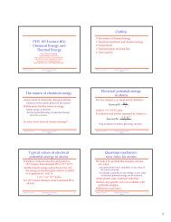
Optical energy stored in a solar cell generates electrons and<br />
holes (e - & h + ) through a photoelectric effect; these give rise to<br />
the electrical current from the working cell. For thicker solar<br />
cells, the energy storage is dominated by photons rattling<br />
around the semiconductor layer. The figure illustrates the<br />
transverse electric field E for photons propagating to the right<br />
(with wavevector k) near the interface of a metal contact and<br />
the semiconductor. It is also possible to store optical energy in<br />
surface plasmons that propagate along the metalsemiconductor<br />
interface; the figure illustrates the longitudinal<br />
(!) electric field for these. Storing optical energy as both photons<br />
and plasmons increases the efficiency with which the<br />
solar cell absorbs sunlight.