Microchip Manufacturing
Microchip Manufacturing
Microchip Manufacturing

Create successful ePaper yourself
Turn your PDF publications into a flip-book with our unique Google optimized e-Paper software.
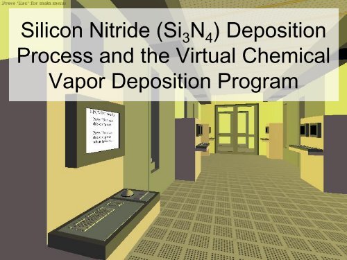
Silicon Nitride (Si 3 N 4 ) Deposition<br />
Process and the Virtual Chemical<br />
Vapor Deposition Program
Chemical Vapor Deposition A Closer Look: Si 3 N 4<br />
Overall Reaction:<br />
3 SiCl 2 H 2 (g) + 10 NH 3 (g) Si 3 N 4 (s)<br />
Dichlorosilane<br />
(DCS)<br />
Ammonia<br />
Silicon<br />
nitride<br />
+<br />
6 NH 4 Cl (g) +<br />
Ammonium chloride<br />
6 H 2 (g)<br />
Hydrogen<br />
NH 3 (gas)<br />
NH 4 Cl (gas)<br />
H 2 (gas) SiCl 2 H 2 (gas)<br />
Silicon<br />
nitride<br />
SiCl 2 H 2 (gas)<br />
NH 3 (gas)<br />
Graphics copy-write Pro. Milo Koretsky, Chemical Engineering Department at OSU<br />
Photo Courtesy of Silicon Run Educational Video
Chemical Vapor Deposition A Closer Look:<br />
Factors that Effect Film Thickness and Uniformity<br />
• Absolute flow rates of ammonia<br />
to DCS<br />
• Ratio of ammonia to DCS (fixed)<br />
• Temperature (5 zones)<br />
• Reaction time<br />
• Pressure (fixed)<br />
We’ll explore the results of changing<br />
some of these factors.<br />
DCS (gas)<br />
NH 3 (gas)<br />
NH 4 Cl (gas)<br />
H 2 (gas)<br />
NH 3 (gas)<br />
DCS (gas)<br />
Thickness<br />
Film<br />
Substrate
Virtual CVD Overview<br />
Choosing the Virtual CVD reactor parameters<br />
Pressure<br />
is Fixed<br />
Each run costs $
Film Thickness [A]<br />
Film Thickness [A]<br />
Measurement – Thickness & Uniformity<br />
• Film thickness is determined by the amount of material<br />
that reacts and is grown on the wafer<br />
• Uniformity describes the evenness of film thickness on<br />
the wafer<br />
45% Uniformity 100% Uniformity<br />
1000<br />
1000<br />
800<br />
600<br />
400<br />
200<br />
0<br />
-150 -50 50 150<br />
x position<br />
800<br />
600<br />
400<br />
200<br />
0<br />
-150 -50 50 150<br />
x position
Wafer #<br />
Measurement – Thickness & Uniformity<br />
• Film thickness is determined by the amount of material<br />
that reacts and is grown on the wafer<br />
• Uniformity describes the evenness of film thickness on<br />
the wafer<br />
NH 4 Cl (gas)<br />
H 2 (gas)<br />
NH 3 (gas)<br />
200<br />
150<br />
50% Overall Efficiency<br />
SiCl 2 H 2 (gas)<br />
0<br />
100<br />
50<br />
SiCl 2 H 2 (gas)<br />
NH 3 (gas)<br />
79% Overall Efficiency<br />
0 2000 4000 6000 8000 10000<br />
Thickness [A]
Measurement via Ellipsometer<br />
• The ellipsometer is used to measure the<br />
thickness and refractive index of<br />
transparent films.<br />
• It is made of a light source and polarizer<br />
on one side and a analyzer and detector<br />
on the other side.<br />
Detector<br />
Analyzing<br />
Polarizer<br />
Substrate<br />
Light Control<br />
Light Source<br />
Polarizing<br />
Sheet<br />
Analyzer &<br />
Detector<br />
Light Source,<br />
Control &<br />
Polarizing<br />
Sheet<br />
• Light from the source is polarized<br />
and reflected off the film.<br />
• The analyzer is rotated till no light<br />
passes through it.<br />
• The angle of rotation depends on the<br />
thickness of the film.
Virtual CVD Overview<br />
Choosing the locations on the wafer to measure<br />
Each measurement costs $
Virtual Chemical Vapor Deposition<br />
(VCVD) Program<br />
VCVD Program<br />
Semiconductor <strong>Manufacturing</strong> Fab<br />
Photo Courtesy of http://webmedia.national.com/gallery/06/06_rgb.jpg
Your Objectives:<br />
•Optimize “Recipe”<br />
◦high uniformity (within wafer and between wafers)<br />
◦meets a target thickness of 1000 Angstroms<br />
•Minimize Cost
Let’s Get Started<br />
•Open VCVD Program...