Focused ion beam technology, capabilities and ... - FEI Company
Focused ion beam technology, capabilities and ... - FEI Company
Focused ion beam technology, capabilities and ... - FEI Company

You also want an ePaper? Increase the reach of your titles
YUMPU automatically turns print PDFs into web optimized ePapers that Google loves.
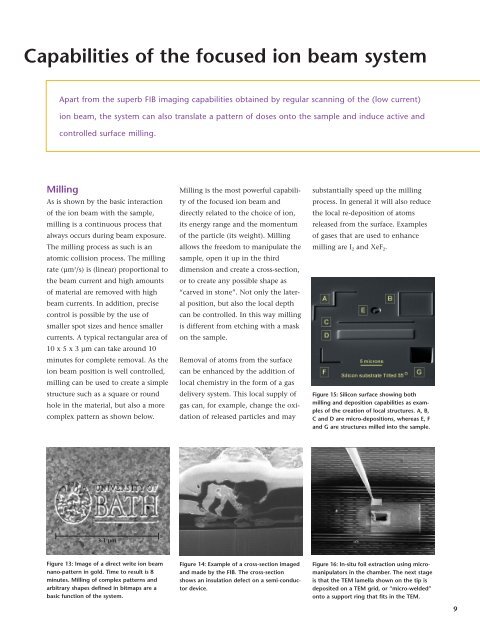
Capabilities of the focused <strong>ion</strong> <strong>beam</strong> system<br />
Apart from the superb FIB imaging <strong>capabilities</strong> obtained by regular scanning of the (low current)<br />
<strong>ion</strong> <strong>beam</strong>, the system can also translate a pattern of doses onto the sample <strong>and</strong> induce active <strong>and</strong><br />
controlled surface milling.<br />
Milling<br />
As is shown by the basic interact<strong>ion</strong><br />
of the <strong>ion</strong> <strong>beam</strong> with the sample,<br />
milling is a continuous process that<br />
always occurs during <strong>beam</strong> exposure.<br />
The milling process as such is an<br />
atomic collis<strong>ion</strong> process. The milling<br />
rate (µm3 /s) is (linear) proport<strong>ion</strong>al to<br />
the <strong>beam</strong> current <strong>and</strong> high amounts<br />
of material are removed with high<br />
<strong>beam</strong> currents. In addit<strong>ion</strong>, precise<br />
control is possible by the use of<br />
smaller spot sizes <strong>and</strong> hence smaller<br />
currents. A typical rectangular area of<br />
10 x 5 x 3 µm can take around 10<br />
minutes for complete removal. As the<br />
<strong>ion</strong> <strong>beam</strong> posit<strong>ion</strong> is well controlled,<br />
milling can be used to create a simple<br />
structure such as a square or round<br />
hole in the material, but also a more<br />
complex pattern as shown below.<br />
3.1 µm<br />
Figure 13: Image of a direct write <strong>ion</strong> <strong>beam</strong><br />
nano-pattern in gold. Time to result is 8<br />
minutes. Milling of complex patterns <strong>and</strong><br />
arbitrary shapes defined in bitmaps are a<br />
basic funct<strong>ion</strong> of the system.<br />
Milling is the most powerful capability<br />
of the focused <strong>ion</strong> <strong>beam</strong> <strong>and</strong><br />
directly related to the choice of <strong>ion</strong>,<br />
its energy range <strong>and</strong> the momentum<br />
of the particle (its weight). Milling<br />
allows the freedom to manipulate the<br />
sample, open it up in the third<br />
dimens<strong>ion</strong> <strong>and</strong> create a cross-sect<strong>ion</strong>,<br />
or to create any possible shape as<br />
“carved in stone”. Not only the lateral<br />
posit<strong>ion</strong>, but also the local depth<br />
can be controlled. In this way milling<br />
is different from etching with a mask<br />
on the sample.<br />
Removal of atoms from the surface<br />
can be enhanced by the addit<strong>ion</strong> of<br />
local chemistry in the form of a gas<br />
delivery system. This local supply of<br />
gas can, for example, change the oxidat<strong>ion</strong><br />
of released particles <strong>and</strong> may<br />
Figure 14: Example of a cross-sect<strong>ion</strong> imaged<br />
<strong>and</strong> made by the FIB. The cross-sect<strong>ion</strong><br />
shows an insulat<strong>ion</strong> defect on a semi-conductor<br />
device.<br />
substantially speed up the milling<br />
process. In general it will also reduce<br />
the local re-deposit<strong>ion</strong> of atoms<br />
released from the surface. Examples<br />
of gases that are used to enhance<br />
milling are I2 <strong>and</strong> XeF2. Figure 15: Silicon surface showing both<br />
milling <strong>and</strong> deposit<strong>ion</strong> <strong>capabilities</strong> as examples<br />
of the creat<strong>ion</strong> of local structures. A, B,<br />
C <strong>and</strong> D are micro-deposit<strong>ion</strong>s, whereas E, F<br />
<strong>and</strong> G are structures milled into the sample.<br />
Figure 16: In-situ foil extract<strong>ion</strong> using micromanipulators<br />
in the chamber. The next stage<br />
is that the TEM lamella shown on the tip is<br />
deposited on a TEM grid, or “micro-welded”<br />
onto a support ring that fits in the TEM.<br />
9