1973-02-03
1973-02-03
1973-02-03

Create successful ePaper yourself
Turn your PDF publications into a flip-book with our unique Google optimized e-Paper software.
Il<br />
Il<br />
II<br />
II<br />
Il<br />
11
We are living in an era of rapid and apparently unending advances in<br />
technology -so much so that the expression "exciting challenge" has become<br />
almost shop worn. Nonetheless, I believe the challenges of new technology in<br />
the radar and antenna design areas today are as exciting and stimulating as<br />
anything we have seen in this field since the early days of bedspring antennas.<br />
For years some form of the dish antenna was the bread and butter of the radar<br />
designer; feed techniques were the chief source of modifying sensor<br />
performance, but antenna design remained relatively stable. Communications<br />
systems and their antennas showed a similar sameness, remarkable more for the<br />
apparent static nature of antenna design than for any other feature.<br />
But no more. For more than ten years now we have been involved with all the<br />
problems and attendant opportunities of electronically steered array<br />
radars -the flat -faced array has arrived. Further, we've seen great antenna fields<br />
spreading over acres of land serving as antenna systems for high- frequency<br />
radars. Space work has opened up a virtually unlimited new area for imaginative<br />
antenna design. Even the staid old broadcast antenna is developing new dimensions<br />
and encountering new problems.<br />
The challenges are not limited to antennas alone. Computer control of radars is<br />
growing apace, presenting a whole new dimension of problems and -more important-<br />
opportunities for building better systems at lower cost. Moreover,<br />
refinements in technology now make it possible to obtain so much information<br />
that signal processing and data processing systems must be capable of<br />
immensely complex real -time performance.<br />
Perhaps the greatest challenge of all has come in the area of designing to cost.<br />
All modern major systems are inherently expensive, and Government funding<br />
for development effort has been unable to keep up with the capacity of our<br />
engineers to evolve more complex (and more costly) equipment. Accordingly,<br />
many of the most important technological advances in recent years have come<br />
from concerted efforts to provide performance at the lowest possible cost.<br />
These, then, are some of the challenges and opportunities that make the radar<br />
and antenna field a very exciting venture and promise even greater challenge as<br />
the technology continues to unfold.<br />
Editor<br />
Associate Editor<br />
Art Editor<br />
Editorial Secretary<br />
Subscriptions<br />
Composition<br />
Technical Publications Adm.,<br />
Electronic Components<br />
Technical Publications Adm.,<br />
Laboratories<br />
Technical Publications Adm.,<br />
Corporate Engineering Services<br />
Mgr., Quality and Reliability<br />
Assurance, Solid State Div.<br />
VP, Engineering, NBC<br />
Television Network<br />
Mgr., Technical Information<br />
Services, RCA Laboratories<br />
Manager, Consumer Products<br />
Adm., RCA Service Co.<br />
Chief Engineer,<br />
Record Division<br />
Chief Technical Advisor,<br />
Consumer Electronics<br />
Div. VP, Technical Planning<br />
Electronic Components<br />
Staff VP, Engineering<br />
Exec. VP, Leased Facilities<br />
and Engineering,<br />
Global Communications, Inc.<br />
Manager, Engineering<br />
Professional Development<br />
Division VP,<br />
Government Engineering<br />
Dudley M. Cottler<br />
Chief Engineer<br />
Missile and Surface Radar Division<br />
Moorestown, New Jersey<br />
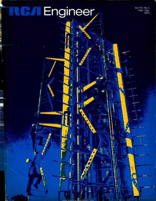
Our cover<br />
... features part of a new broadcast antenna complex being<br />
planned for the World Trade Center (New York City)<br />
installation. Climbing the antenna are engineer Frank<br />
Chwieroth (lower left) and wiremen Richard Carver (top<br />
left), Harold James (center), and Harry Crowthers (top<br />
right). Photo credit: Bill Eisenberg, GCS, Camden.
J.<br />
Dr.<br />
M.<br />
W.<br />
Dr.<br />
W.<br />
D.<br />
A.<br />
E.<br />
A.<br />
Vol. 18, No. 5<br />
Feb Mar<br />
<strong>1973</strong><br />
A technical journal published by<br />
RCA Corporate Engineering Services 2 -8,<br />
Camden, N.J.<br />
RCA Engineer articles are indexed<br />
annually in the April -May Issue and<br />
in the "Index to RCA Technical Papers."<br />
[ECM Engineer<br />
To disseminate to RCA engineers technical<br />
information of professional value To publish<br />
in an appropriate manner important technical<br />
developments at RCA, and the role of the engineer<br />
To serve as a medium of interchange of<br />
technical information between various groups<br />
at RCA To create a community of engineering<br />
interest within the company by stressing<br />
the interrelated nature of all technical contributions<br />
To help publicize engineering<br />
achievements in a manner that will promote<br />
the interests and reputation of RCA in the<br />
engineering field To provide a convenient<br />
means by which the RCA engineer may review<br />
his professional work before associates<br />
and engineering management To announce<br />
outstanding and unusual achievements of<br />
RCA engineers in a manner most likely<br />
to enhance their prestige and professional<br />
status.<br />
Contents<br />
Theme -radar, communication, and antennas<br />
Editorial input Reprints of RCA Engineer Articles J. P. Dunn 2<br />
Special Four RCA men elected IEEE Fellows 4<br />
Engineer and the Corporation Television receiving antennas in blue and gold. J. D. Callaghan I<br />
W. Peterson 6<br />
G &CS antenna range W. C. Wilkinson 11<br />
Broadcast antennas New VHF Filterplexer D. G. Hymas I<br />
J. Matta P. C. Nole I<br />
N. Schmitz 15<br />
Computer -aided design of vertical patterns for TV antennas Dr. Krishma Praba 18<br />
Radar Lunar sounder experiment for Apollo 17 Dr. S. L. Goldman<br />
I<br />
J. Nossen 22<br />
I<br />
Displays for modern radar systems G. A. Senior 26<br />
Phase shifter and driver design for the AN /SPY -1 phased array N. R. Landry H. C. Goodrich 29<br />
High- efficiency avalanche diodes (TRAPATT) Dr. K. K. N. Chang H. Kawamoto<br />
I I<br />
for phased -array radar systems Dr. V. A. Mikenas H. J. Prager J. Reynolds Rosen 34<br />
I I<br />
Communication<br />
High power latching ferrite phase shifters for AEGIS<br />
High- frequency high -power multi- octave distributed -amplifier transmitter<br />
Low backlobe antenna for airborne missile -warning system<br />
Ultra- lightweight deployable antennas<br />
L. J. Lavedan, Jr. 40<br />
D. L. Pruitt 44<br />
H. Honda 48<br />
W. S. Sepich 53<br />
Communication antennas for Viking Mars Lander W. C. Wilkinson<br />
I<br />
A. Harmening<br />
I<br />
O. M. Woodward 56<br />
Decoder for delay -modulation coded data J. Lewin 60<br />
Simple analytical model for the envelope distribution for a sinusoidal carrier in<br />
atmospheric radio noise C. V. Greenman 64<br />
Engineer and the Corporation RCA -MIT Research Conference W. O. Hadlock 66<br />
General interest Advanced packaging with thin -film microcircuits W. J. Grieg<br />
I<br />
R. Brown 74<br />
Charge -coupled devices and applications J. E. Carnes<br />
I<br />
F. Kosonocky 78<br />
Engineering and<br />
Research Notes<br />
Analog to digital (rolling sample) correlator H. C. Goodrich I E. C. Farnett 86<br />
Self- contained impact detector and reporter A. J. Lisicky<br />
I<br />
G. Staton I E. D. Grim 87<br />
Departments Pen and Podium 88<br />
Patents Granted 90<br />
Dates and Deadlines 91<br />
News and Highlights 93<br />
Copyright <strong>1973</strong><br />
All rights reserved
Reprints of RCA Engineer<br />
00 articles<br />
J. P. Dunn, Art Editor<br />
Although the RCA Engineer can be distributed only inside RCA, reprints of articles<br />
from any issue can be supplied quickly and economically, and may go to customers,<br />
opinion leaders, prospective employees, or students. RCA Technical Publications<br />
staff provides these reprints to divisions wishing to promote their products or to<br />
provide their clients, prospects, and customers with valuable information.<br />
Hd.4<br />
,6,e,,,e<br />
AS<br />
MANY OF OUR READERS KNOW, arti-<br />
cles appearing in the RCA Engineer<br />
can be reprinted on a single<br />
article basis or as an anthology of<br />
several articles (from several issues)<br />
devoted to a single theme, technology,<br />
or facility. Covers for reprints<br />
may be custom designed to<br />
suit a specific purpose. Assistance<br />
in cover design, brochure content,<br />
and utilization of reprints will be<br />
provided by the RCA Engineer editorial<br />
staff.<br />
Varied uses<br />
Over 100,000 copies per year of reprints<br />
of RCA Engineer articles are<br />
used by the various divisions<br />
throughout the company. Orders<br />
have varied from simple two -page<br />
leaflets to a 200 -page brochure with<br />
a full -color cover. Reprints are valuable<br />
for many purposes:<br />
as informative brochures or descriptive<br />
bulletins;<br />
to display engineering and technical<br />
skills;<br />
for marketing and sales mailings<br />
and handouts;<br />
for mailings to prospects. customers,<br />
and opinion leaders;<br />
for answering any inquiries that require<br />
technical explanations;<br />
for use with commercial and government<br />
proposals; and<br />
to give to personnel groups for<br />
orientation, training and recruiting.<br />
An additional fifty copies of each<br />
reprint ordered is kept on file by<br />
Staff Technical Publications, and a<br />
limited amount of these is available,<br />
should a division need backup. Certain<br />
other comprehensive booklets<br />
become available from time to time<br />
Heprint RE-18-5-9<br />
(usually an announcement is made<br />
in Trend) and limited quantities can<br />
be ordered by phoning or writing<br />
the RCA Engineer editorial office.<br />
(See section titled "How to Order ".)<br />
A catalogue listing all RCA Engineer<br />
reprints is available from your<br />
division TPA or library.<br />
Covers<br />
Single articles<br />
On single -article reprints, a simple<br />
title page imprint (article title, author,<br />
RCA logotype, and division) is<br />
included when a blank page is<br />
available. For economy, reprints<br />
are prepared in increments of four<br />
pages each; thus, a three -page article<br />
would be printed as a four -<br />
page reprint with the extra page<br />
used as a cover. In a four -page article,<br />
the cover information is placed<br />
on the title page of the article unless<br />
the separate title page is requested;<br />
the four -page article is<br />
then handled (and priced) as an<br />
eight -page reprint.<br />
Booklets<br />
On booklet reprints, covers are custom-<br />
designed to suit the "theme"<br />
of the articles, using typography and<br />
artwork to suit. These booklets can<br />
also utilize previous RCA Engineer<br />
covers in either full color or in<br />
black- and -white. Cover messages,<br />
marketing contacts, or other additional<br />
information appropriate to the<br />
purpose of the booklet may be<br />
placed on the inside front and back<br />
covers.<br />
2
Cost and delivery<br />
Delivery<br />
Four- and eight -page reprints can<br />
be supplied within two weeks of the<br />
receipt of the order. Reprint booklets<br />
are available on a four-to- eightweek<br />
time cycle, depending on the<br />
complexity of the additional cover<br />
material. Rush schedules may affect<br />
price and are handled on an individual<br />
basis.<br />
Cost<br />
Approximate prices for various reprints<br />
are tabulated below.<br />
How to order<br />
All policy on reprint content, availability<br />
and utilization is administered<br />
by the RCA Engineer editorial<br />
staff, since additional changes must<br />
be made to reprints before they can<br />
be distributed. Reprints can be obtained<br />
only through the RCA Engineer<br />
editorial office, RCA Building<br />
2 -8, Camden, N.J. For rush orders,<br />
phone WO 3 -8000, Ext. PC -4018. The<br />
following information must be supplied<br />
with order:<br />
1) Article or articles desired;<br />
2) Special instructions on cover requirements<br />
or special information<br />
to be added;<br />
3) Quantity desired;<br />
4) Delivery requirements (time and<br />
place); and<br />
5) Account No. (not a purchase order).<br />
An RCA Engineer article reprint is<br />
an easy, economical way to promote<br />
the work of your division. If you've<br />
never availed yourself of this useful<br />
service, or just haven't thought<br />
about it lately, we'd like to suggest<br />
that you try it.<br />
Reprint price list<br />
Quantity<br />
Size of<br />
reprint (pages) 100 500<br />
Self 2 20.00 22.00<br />
cover 4 38.00 41.00<br />
8 70.40 88.00<br />
12 84.70 123.20<br />
16 89.10 128.70<br />
With /- 32 237.60 328.90<br />
color 48 382.80 476.30<br />
enamel 64 429.00 616.00<br />
cover 72 540.10 715.00<br />
80 600.60 825.00<br />
86 697.40 891.00<br />
96 792.00 995.50<br />
Additional<br />
1000 2500 5000 7500 10,000 1000's<br />
27.00 51.00 68.20 84.70 104.50 9.00<br />
47.00 99.00 126.50 170.50 198.00 17.00<br />
104.50 209.00 3<strong>02</strong>.50 444.40 554.40 50.00<br />
171.60 257.40 481.80 664.40 830.50 75.00<br />
177.10 268.40 492.80 680.90 869.00 79.00<br />
425.70 630.30 1,150.00 1,570.00 1,910.00 174.00<br />
594.00 976.80 1,578.00 2,151.00 2,695.00 246.00<br />
764.50 ,250.00 2,005.00 2,719.00 3.350.00 320.00<br />
869.00 ,450.00 2,250.00 2,990.00 3,750.00 330.00<br />
946.00 ,550.00 2,440.00 3,310.00 4,140.00 360.00<br />
1,045.00 .640.00 2,610.00 3,515.00 4,405.00 390.00<br />
1,140.00 ,730.00 2,805.00 3,880.00 4,780.00 455.00<br />
Cost for 4 -color cover: add this cost to<br />
the price shown above for reprints with<br />
I -color enamel covers (color covers are<br />
picked up from an existing RCA Engineer cover.)<br />
305.00 380.00 450.00 515.00 590.00 56.00<br />
Extra typesetting is added to the above prices (e.g., for an added table of contents in booklets.)<br />
3
Four RCA men<br />
elected<br />
IEEE Fellows<br />
The four RCA men cited herein have been honored for<br />
their professional achievements by being elected Fellows<br />
of the Institute of Electrical and Electronics Engineers.<br />
This recognition is extended each year by the IEEE to<br />
those who have made outstanding contributions to the<br />
field of electronics.<br />
Dr. Heilmeier (now on leave of absence) was Head of the Device Concepts Research<br />
Group at RCA Laboratories before being appointed a White House Fellow, assigned to<br />
the Department of Defense, in September, 1970. In September 1971, Secretary of<br />
Defense Melvin Laird appointed Dr. Heilmeier Assistant Director of Defense Research<br />
and Engineering (Electronics and Computer Sciences).<br />
Dr. Heilmeier received the BSEE (with distinguished honors) from the University of<br />
Pennsylvania in 1958, and the MSE, MA, and PhD in solid state materials and electronics<br />
from Princeton in 1960, 1961, and 1962, respectively. His work at Princeton University<br />
was done under the sponsorship of the RCA Laboratories. In 1960 he received the RCA<br />
Laboratories Achievement Award for his work in parametric and tunnel diode devices,<br />
in 1962 for pioneering work in the field of crystalline organic semiconductors, and in<br />
1965 for research in the area of liquid crystalline phenomena. He as received two IR -100<br />
awards (1968, 1969) for outstanding new product developments in the field of liquid<br />
crystal display devices. He was also a co- recipient of the 1969 David Sarnoff Outstanding<br />
Team Award in Science for "basic studies of liquid crystals with imaginative ideas<br />
for their application to practical display." In March of 1968 he was the recipient of one of<br />
the "Outstanding Young Electrical Engineer" awards of Eta Kappa Nu. In March of 1969<br />
he received the Eta Kappa Nu award as the "Outstanding Young Electrical Engineer in<br />
the U.S.A."<br />
Dr. Heilmeier has fifteen U.S. patents issued or pending and has published or presented<br />
over 40 papers in the areas of microwave solid state devices, organic semiconductors,<br />
adaptive thin film ferroelectric devices, solid state devices, optical modulators and displays.<br />
In 1966 he became the Head of the Solid and Liquid State Device Research Group at<br />
RCA Laboratories and Head of the Device Concepts Research Group in 1968.<br />
Barton Kreuzer, Executive Vice President, RCA Corporate Headquarters, New York,<br />
N.Y., was appointed Executive Vice President, Consumer Electronics, of RCA in<br />
December 1969 and held that post until December 1972.<br />
As Executive Vice President, Consumer Electronics, Mr Kreuzer was responsible for the<br />
world -wide operation of RCA Consumer Electronics, which manufactures television<br />
sets, radios and other consumer products, and also includes the RCA Sales<br />
Corporation and RCA Distributing Corp. Mr. Kreuzer formerly was Executive Vice<br />
President, Commercial Electronics Systems, with headquarters in Camden, N.J. Prior<br />
to that he had served since June, 1968 as Vice President and General Manager of the<br />
division. Earlier, Mr. Kreuzer was Division Vice President and General Manager,<br />
Commercial Electronic Systems Division, a post to which he was named in August,<br />
1967. Before this assignment he served for more than seven years as Division Vice<br />
President and General Manager, Astro- Electronics Division. He joined that Division<br />
when it was formed in 1958 as Manager of Marketing and became its head in 1960.<br />
Mr. Kreuzer joined RCA in 1928, after receiving the BSEE Electrical Engineering from<br />
Brooklyn Polytechnic Institute. As a young engineer, he helped establish RCA's<br />
pioneer television station, W2XBS, in New York City, in 1928 -29. In 1935, Mr. Kreuzer<br />
became head of RCA film -recording equipment sales in the East, and six years later was<br />
named national manager. He was appointed Manager of RCA Theater Equipment activities<br />
in 1943. His promotion in 1946 to Manager, RCA Industrial Products<br />
Department, made him responsible for a wide range of products in the industrial and<br />
commercial electronics field. Mr. Kreuzer in 1950 was named General Product Manager<br />
of the former Engineering Products Division which produced defense, broadcast, communications,<br />
and industrial electronic systems. In 1954, he was appointed Director of<br />
Product Planning on the RCA Corporate Staff, a post he held until 1958 when he joined<br />
the newly established Astro- Electronics Division.<br />
Mr Kreuzer is a former President of the SMPTE of which he continues as a Fellow. Mr.<br />
Kreuzer is a director of RCA Ltd. (Canada) and of RCA Ltd. (Taiwan).<br />
4
Editor's note: In addition to these four recipients, three<br />
past RCA employees received the grade of Fellow from<br />
IEEE: Julian J. Bussgang, formerly with Aerospace<br />
Systems Division, Burlington, Mass., "for contributions to<br />
sequential detection theory, radar techniques, and statistical<br />
communications, "; Dr. Joseph J. Loferski, formerly<br />
with RCA Laboratories, "for contributions to radiation<br />
damage in semiconductors, solar cell technology, and<br />
education; and Arthur W. Vance, formerly with RCA<br />
Laboratories and Astro- Electronics Division, "for pioneering<br />
contributions to television, electronic instruments,<br />
regulated power supplies, weapons systems, and<br />
simulators."<br />
Dr. Sobol, Head, Communications Technology Research, Communications Research<br />
Laboratory, RCA Laboratories, Princeton, N.J. presently directs a research group<br />
concerned with the development of new microwave devices and technology for communication<br />
systems.<br />
Dr. Sobol received the BSEE from the City College of New York in 1952. He then<br />
attended the University of Michigan, receiving the MS and PhD in Electrical Engineering<br />
in 1955 and 1959, respectively. From 1952 to 1959, he did research in the radar,<br />
weapon guidance, and microwave fields at the Willow Run and Electron Physics<br />
Laboratories of the University of Michigan.<br />
From 1960 to 1962, Dr. Sobol investigated superconducting films at the IBM Watson<br />
Research Center. He joined the Microwave Research Laboratory, RCA Laboratories in<br />
1962. A year later he was named Head of Power Generation Research and in 1965, Head,<br />
Microwave Integrated Circuits Research. In the latter position, he directed the research<br />
and development of microwave integrated circuits in RCA's corporate -wide Blue Chip<br />
Program.<br />
He was Manager, Microwave Microelectronics, at the RCA Solid State Division in<br />
Somerville, N.J., from 1968 to 1970. Under his direction, the basic technology for<br />
fabricating microwave integrated circuits was advanced from laboratory status to a<br />
pilot production. He then served as a Corporate Staff Engineer from 1970 until his<br />
present appointment.<br />
Dr. Sobol is a member of the American Physical Society, Eta Kappa Nu, Tau Beta Pi,<br />
Sigma Xi and Phi Kappa Phi.<br />
He held a Sperry Fellowship in Electron Physics during 1955 -1956 and was the IEEE<br />
1970 National Lecturer in Microwaves. Dr. Sobol is listed in Who's Who in the East and<br />
American Men of Science. He is author or co- author of 28 papers in technical journals<br />
and has presented more than 35 papers at technical meetings.<br />
He was an Adjunct Lecturer in the Graduate School at Drexel University during 1963<br />
and 1964. He has lectured for several University of Michigan Summer Courses.<br />
Dr. Urkowitz, Missile and Surface Radar Division, Moorestown, N.J received the BSEE<br />
from Drexel University in 1948, and the MSEE and PhD from the University of<br />
Pennsylvania in 1954 and 1972, respectively. He was employed by the Philco<br />
Corporation from 1948 to 1964, and by General Atronics Corporation from 1964 to<br />
1970. He joined the RCA Missile and Surface Radar Division in 1970, where he is on the<br />
Scientific Staff of the Systems Engineering Department.<br />
Throughout his industrial career, Dr. Urkowitz has been involved in the analysis and<br />
design of signal processing techniques, particularly for signals which have been<br />
corrupted by, besides additive noise, unwanted clutter reflection and by passage<br />
through random and /or time varying media. His studies have been applied to radar,<br />
sonar, scatter communication, and to the processing of seismic signals.<br />
He is the author of more than 30 technical papers and has presented many papers to<br />
scientific meetings.<br />
Dr. Urkowitz is a member of the Information Theory and Aerospace and Electronic<br />
Systems Groups of the IEEE. He is a past chairman of the Philadelphia Chapter, IEEE<br />
Group on Circuit Theory, a founder and the first chairman of the Philadelphia Chapter,<br />
IEEE Group on Information Theory. He has served on the IEEE Philadelphia Section<br />
Meetings Committee and for several years was an industry representative to the Subcommittee<br />
on Ultrasonic Delay Lines of the Electronic Industries Association. He is<br />
presently chairman of the Signal Theory Subcommittee, Standards Coordinating Committee,<br />
IEEE Group on Information Theory.<br />
Dr. Urkowitz is an adjunct professor of electrical engineering at Drexel University's<br />
Graduate School of Engineering, where he presently teaches a course in stochastic<br />
processes. He has been associated with the graduate faculty since 1952. He introduced.<br />
wrote the texts, and taught the first graduate courses in modern netweork theory and in<br />
stochastic processes as applied to electrical engineering.<br />
5
Television receiving<br />
antennas in blue and gold<br />
J. D. Callaghan' D. W. Peterson<br />
The profitable television receiving antenna product -line, being designed and produced by<br />
RCA Parts and Accessories, demonstrates the success that can be obtained by entrepreneurship<br />
within divisional boundaries of a large corporation. The necessary elements<br />
of such success are the recognition of a viable market, the ability to reach it, and the talent<br />
to produce product at a competitive cost. Add a management team with the wisdom and<br />
foresight to identify and exploit these elements and the courage to make the necessary<br />
investment and the result is a new area of profit where none had previously existed. This<br />
paper describes the engineering effort behind the development of the current RCA<br />
product line of "blue and gold" TV receiving antennas and how its success has paved the<br />
way for the introduction of other product lines into market areas previously untouched by<br />
RCA.<br />
RCA PIONEERED in the design and<br />
sale of television receiving antennas.<br />
However, the antenna business was only<br />
an adjunct to the home instrument<br />
business and, as such. was isolated from<br />
the mainstream of television receiver<br />
design and manufacture. Consequently.<br />
RCA was an early dropout.<br />
In 196h, the RCA Parts and Accessories<br />
Division at Deptford, New Jersey, reentered<br />
the receiving antenna business<br />
and, in 1970, introduced a new line of<br />
RCA -designed antennas: this new line<br />
has proven to be an outstanding success.<br />
The "Permacolor" antenna line illustrates<br />
how RCA may profitably enter well -established<br />
small markets.<br />
The television receiving antenna industry<br />
produces a national aggregate gross income<br />
of about $50- million annually and<br />
is dominated by several relatively small<br />
manufacturers who have been in existence<br />
from the early days of TV. For<br />
most of the major manufacturers, antennas<br />
represent a substantial proportion of<br />
their total business. This means that they<br />
must organize their manufacturing along<br />
quite simple and efficient lines to make<br />
their product highly cost competitive. To<br />
re -enter this business, RCA had to implement<br />
an effective plan which would<br />
entail full control of engineering,<br />
manufacturing, and marketing -a plan<br />
that would equal or exceed the efficiency<br />
of major competitors.<br />
This was accomplished through several<br />
phases. The first phase involved specifying<br />
and procuring a line of antennas from<br />
Reprint RE- 18 -5 -5<br />
Final manuscript received November 29, 1972.<br />
6
a competitor for exclusive sale by RCA.<br />
There are many drawbacks to buying<br />
from a competitor; but there was no other<br />
practical way since, at the outset, it had<br />
been decided that marketing,<br />
engineering, and manufacturing<br />
organizations were to be established on a<br />
pay as- as- you -go basis utilizing profits<br />
from antenna sales. There are several major<br />
drawbacks to this approach:<br />
I ) A necessary economy in marketing antennas<br />
is the drop shipping of finished goods from<br />
factory to distributor. Thus, the competitor<br />
knows at all times who the RCA customers<br />
are; he knows their level of purchases; and<br />
can approach the more attractive accounts<br />
on the sale of their own "original" brand.<br />
2)The antennas are easily recognized in the<br />
marketplace as the competitor's product, a<br />
decided product identity disadvantage.<br />
3) RCA, as an intermediary between<br />
manufacturer. and distributor, must mark<br />
up the cost whereas a merchandising<br />
manufacturer can sell directly to<br />
distributors without this additional mark<br />
up. This cost disadvantage is probably the<br />
most serious drawback.<br />
Nevertheless, Parts & Accessories established<br />
an aggressive marketing<br />
organization which has been able to build<br />
sales to an attractive level.<br />
Once the ability to achieve a significant<br />
share of this market was established, the<br />
next step was to develop a highly distinctive<br />
line of antennas that could be<br />
produced by a non -competitive manufacturing<br />
source or by an RCA production<br />
facility. To accomplish this next phase,<br />
additional engineering and support personnel<br />
were hired and an engineering<br />
facility was designed and constructed.<br />
Antenna development facility<br />
Antenna development and design requires<br />
a special facility which must include<br />
outdoor antenna testing ranges.<br />
Such a facility was planned and built at<br />
Deptford, N.J., in 1968. Radio -wave<br />
reflections from an adjacent building can<br />
seriously limit the capabilities of an<br />
antenna range, so the antenna building<br />
was designed to minimize these reflections.<br />
Since television broadcasting employs<br />
horizontally polarized radiation,<br />
transverse horizontal wiring and plumbing<br />
in the building was avoided. Radio -<br />
frequency measurements of building<br />
materials were made as the basis for<br />
choosing non -reflecting materials. The<br />
sidewa Ils of the frame structure made use<br />
of vinyl siding with Celotex sheathing<br />
and interior walls, materials with far<br />
Fig. - 1 Antenna development facility at<br />
Deptford. The curved radio -transparent<br />
wall used for "indoor" testing of antennas<br />
is at this end of the building.<br />
lower reflection coefficients than most<br />
building materials. The roof material was<br />
corrugated fiberglass sheet. The net result<br />
was a building unusually free of radio -<br />
wave reflections.<br />
Special laboratory accommodations<br />
were incorporated in the design of the<br />
building to enable antenna development<br />
and design work to be carried on indoors<br />
despite inclement weather which often<br />
hinders antenna work on a conventional<br />
outdoor range. This "indoor" laboratory<br />
is a room 20 ft high by 30 ft wide by 20 ft<br />
Donald W. Peterson, Mgr., Product Development<br />
Engineering, RCA Parts and Accessories, Deptford, N.J.,<br />
joined RCA as an engineering trainee in 1936 and started<br />
in the radio receiver Service Department in 1937 as a<br />
technical writer. He transferred to the RCA Research<br />
Laboratories in Camden, N.J. in 1940, where his<br />
activities included development and research in<br />
antennas and radio wave propagation. As a member of<br />
the original technical staff of the Priceton Laboratories,<br />
he received a laboratory award and the IRE Scott Helt<br />
award for the development of time domain ref lectometry<br />
for television transmitting antenna testing. He also<br />
received a laboratory award for concepts in UHF broadcasting.<br />
In 1961 he transferred to the Missile and<br />
Surface Radar Division as an antenna development and<br />
design engineer. Projects included development of a<br />
circularly polarized feed for the lunar excursion erectable<br />
TV antenna. He received a citation for work on the "two<br />
pound radar" antenna. In 1967 Mr. Peterson joined Parts<br />
and Accessories where he was responsible for the<br />
development of the RCA line of TV receiving antennas.<br />
J. D. Callaghan, Mgr., Engineering, RCA Parts and<br />
Accessories, Deptford. N.J., was employed by RCA in<br />
1946 as a member of the RCA Service Company Home<br />
Instruments Engineering Department. His responsibilities<br />
included the development and approval of TV<br />
receiving antennas and antenna systems. He also<br />
engaged in the development of color TV test equipment,<br />
TV technician training and liaison between the TV<br />
service activity and Consumer Electronics Engineering.<br />
In addition, he received the RCA Award of Merit in 1951.<br />
In 1959 he joined the RCA Service Company BMEWS<br />
project where he became Engineering Manager with<br />
responsibility for on -site installation check -out and test<br />
of all BMEWS equipment. Mr Callaghan came to RCA<br />
Parts and Accessories in 1964 and organized the present<br />
Engineering group which develops accessory products<br />
such as TV antennas, rotators, signal distribution<br />
systems, color TV test jigs, and automobile stereo tape<br />
players. During the course of his employment with RCA,<br />
Mr. Callaghan has been granted nine U. S. patents.<br />
Fig. 2 -This end of the antenna<br />
development facility shows the tower at<br />
one end of the radiation -pattern<br />
measurement range.<br />
deep. It is situated at one end of the building<br />
and has a 20x30 -ft radio- transparent<br />
window in one wall facing an outdoor<br />
radiating source. The window was<br />
designed "in house "and is considered unique.<br />
It consists of dacron- reinforced vinyl<br />
sheeting stretched across a sturdy wood<br />
frame. The vinyl sheet is edge supported<br />
with heavy elastic ties to produce a<br />
natural tautness. The top and bottom<br />
edges curve outward while the side edges<br />
curve inward. The resulting compound<br />
curvature imparts stability to the sheet,<br />
even in high winds (see Appendix A).<br />
After four years of service, the radio window<br />
shows no deterioration. An outside<br />
view of this radio- transparent wall is<br />
shown in Fig. I.<br />
The indoor test room is ideal for gain and<br />
VSWR measurements. The room is part<br />
of a 100 -ft antenna test range and is used<br />
for gain measurement at all TV frequencies.<br />
An .v -t' plotter makes it possible to<br />
Authors Peterson (left) and Callaghan.<br />
7
plot antenna gain over the entire TV spectrum<br />
automatically in minutes.<br />
Equipment is also available in the room<br />
for automatically plotting VSWR<br />
measurements vs. frequency. The entire<br />
new RCA "Permacolor" outdoor line of<br />
antennas was developed and initial tests<br />
were performed in this room.<br />
The opposite end of the antenna building<br />
houses the operating terminal of a 250 -ft<br />
antenna test range set up primarily for<br />
radiation pattern measurement. The<br />
tower for the range is shown in Fig. 2.<br />
This tower can be lowered onto the building<br />
deck by remote control for access to<br />
the antenna mount. The range is<br />
instrumented with a polar pattern plotter<br />
which operates with a bandwidth of only<br />
5 Hz to eliminate extraneous<br />
interference.<br />
The antenna under test is operated as a<br />
signal source. The range receiving<br />
antenna may thus be situated at the<br />
remote end of the Range where its directional<br />
characteristics are used for<br />
minimizing local TV station interference<br />
to the extent that patterns may be<br />
measured between picture and sound carrier<br />
frequencies of the local TV stations if<br />
desired.<br />
Product development and design<br />
Having planned and built the antenna<br />
facility, the first activity was development<br />
of a complete line of outdoor TV receiving<br />
antennas. This meant that new electrical<br />
and mechanical design concepts<br />
were needed in an art which had been<br />
thoroughly worked over for many years<br />
by experienced competitors.<br />
It was clear at the outset that the new<br />
RCA line would, of necessity, be electrically<br />
similar to competitive lines. All<br />
competitors were using an end fire array<br />
for the V H F portion of the antenna with a<br />
54 -to -88 -MHz and a 174 -to -216 -MHz<br />
band. Fortunately, most of the basic electrical<br />
design ideas came from early RCA<br />
work on HF antennas. Common array<br />
elements for the low VHF and high V H F<br />
bands were obviously desirable for<br />
economy. This required creativeness and,<br />
similarly, the means of incorporating a<br />
UHF antenna for an all- channel line required<br />
new concepts.<br />
Existing competitive antenna designs<br />
were examined early in the program to<br />
Fig. 3- Antenna unfolding and interlocking<br />
apparatus.<br />
assess both their weaknesses and their<br />
strengths. A significant weakness that<br />
was common to all of the popular existing<br />
designs was soon discovered. In each of<br />
these designs, the antennas are packaged<br />
in a folded condition to facilitate storage<br />
and shipment. This requires them to be<br />
unfolded by the installing technician. In<br />
the usual design, each dipole element is<br />
folded by use of a rivet acting as a hinge<br />
pin. The contradiction in concept of setting<br />
the rivet loose enough for hinging<br />
and at the same time tight enough for<br />
reliable electrical conduction makes it<br />
almost inevitable that RF noise will<br />
develop when weathering causes corrosion<br />
at the hinge joint. Here was an opportunity<br />
for design improvement. An<br />
electrical design was developed which<br />
separated the hinge function from the<br />
electrical connecting function. This made<br />
it possible to accomplish a permanent<br />
electrical connection that is immune to<br />
atmospheric deterioration. The strap<br />
which permanently connects the dipole to<br />
the transmission line is solidly riveted and<br />
is shown in Fig. 3. Permanent electrical<br />
connection is further assured by the use of<br />
special..fluted aluminum rivets which cut<br />
into the sides of the holes in the material<br />
being riveted.<br />
A new feature was to overlap the dipoles<br />
at their insulating support. This overlap<br />
provided an easy means of transmission<br />
line transposition by simply reversing the<br />
overlap on successive dipoles. In the final<br />
product, the two halves of the insulator<br />
were designed to unfold and interlock as<br />
shown in Fig. 3, thus providing a<br />
noise -free dipole supporting structure of<br />
great strength.' The overlap also<br />
provided a new means for separating low -<br />
VHF and high -VHF antenna functions.'<br />
The shunt capacity needed to accomplish<br />
separation was provided inexpensively by<br />
merely lengthening the element overlap at<br />
the appropriate place in the array.<br />
Fig. 4 - Model 4BG36 "Permacolor"<br />
antenna.<br />
Another electrical feature introduced in<br />
the design provided for a novel means of<br />
placing low -VHF directors in front of the<br />
high -VHF antenna without degrading<br />
high -VHF performance. This feature was<br />
accomplished by the bugle- shaped<br />
members seen as part of model 4BG36 of<br />
the "Permacolor" line illustrated in Fig. 4.<br />
The UHF antenna was incorporated into<br />
the total configuration by placing a<br />
corner reflector type of antenna in front<br />
of the VH F antenna and tuning the reflector<br />
members to act as directors for the<br />
high VHF band.'<br />
Of economic necessity, the antennas are<br />
fabricated using the same kinds of parts<br />
and material as the competitors use: sheet<br />
metal stampings, butt -seam tubing,<br />
welded tubing, and plastic moldings.<br />
These are all parts that can be fabricated<br />
with high -speed automatic machines to<br />
make them cost competitive. A kit of<br />
about 75 common parts was designed for<br />
this project. From this kit, all of the<br />
antennas needed for a complete line of six<br />
VHF, three UHF, one FM and nine all -<br />
channel antennas could be made. There<br />
are also seven of these models packaged<br />
complete with all installation material<br />
and several types of transmission line for<br />
the do- it- yourself market.<br />
Colors for the new antenna line,<br />
predominately blue with gold support<br />
booms, were adopted by merchandising<br />
to add "eye appeal." The color choice also<br />
represented innovation since all -gold<br />
finish had become standard with the industry.<br />
Even the package size of the product is a<br />
significant cost factor because warehousing<br />
and shipping represent cost just as<br />
surely as do materials and labor. The<br />
antenna was, therefore, designed to be the<br />
ultimate in compactness when folded. All<br />
41410<br />
8
ut four antennas of the I9- antenna<br />
product line are packaged in standard<br />
long, slender cartons that are only 51/4 inches<br />
square. Despite their folded compactness,<br />
the antennas unfold with ease<br />
and lock positively and permanently into<br />
their functioning configuration.<br />
The antennas are marketed by the Parts<br />
and Accessories Division located at<br />
Deptford, N.J. The salesmen reach RCA<br />
Consumer Electronics distributors, as<br />
well as many other independent outlets<br />
throughout the entire nation. Sales<br />
volume has grown to the point where<br />
single distributors often order tractor<br />
trailer -size deliveries.<br />
The advertising of this product has been<br />
both straightforward and effective. The<br />
forthright character of the RCA advertising<br />
makes it stand out in an industry<br />
which has often grossly exaggerated in<br />
their advertising copy.<br />
The RCA product has strong and easily<br />
recognized sales features which give both<br />
the Advertising Department and the<br />
salesmen a story for their customers.<br />
All of the RCA antenna laboratory<br />
products and components are fully<br />
documented within the RCA drawing<br />
system. The general excellence of this<br />
system has permitted both precision and<br />
flexibility in dealing with vendors as well<br />
as tight control of the product in the<br />
antenna factory.<br />
Antenna factory<br />
Most of the metal parts used in production<br />
are fabricated "in- house ". The factory<br />
employs high -speed stamping<br />
machines, rolling mills, piercing<br />
machines, swaging machines, and other<br />
similar equipment. All aluminum sheet<br />
metal is pre -finished before stamping,<br />
rolling, or piercing. Even welded tubing,<br />
which is purchased, is finished before<br />
forming and welding. A tube -bending<br />
machine is shown in Fig. 5. Stamped<br />
parts are produced with automatic<br />
machines at a high rate with progressive<br />
dies. Plastic parts are produced from<br />
RCA molds by suppliers who specialize<br />
in these items.<br />
Antennas are assembled with<br />
automatically fed riveters along a 200 ft<br />
moving belt as shown in Fig. 6. Quality is<br />
assured by inspection of vendor -supplied<br />
parts, and by assembly line inspection.<br />
Antenna quality has remained high from<br />
the start of production.<br />
Entrepeneurship -Parts and Accessories<br />
style<br />
As a business enterprise, RCA<br />
engineering, manufacturing, and marketing<br />
of antennas is an unqualified success.<br />
The product is good, the price is right, the<br />
customers are pleased, and RCA shows a<br />
respectable profit. The entire undertaking<br />
has been carefully tailored to fit<br />
the product with no room for frills. Every<br />
member of the team plays a vital role and<br />
every member knows how he relates to<br />
the overall effort. Morale is high among<br />
the participants because everyone sees<br />
tangible results from his individual efforts.<br />
Business success becomes personal<br />
success.<br />
The antenna activity is integrated as part<br />
of RCA Parts and Accessories.<br />
Marketing, Advertising, Sales, Accounting,<br />
Purchasing, and Engineering<br />
activities are located in Deptford, N.J.<br />
The sales organization operates<br />
throughout the entire United States.<br />
The RCA investment in a sales<br />
organization, an engineering facility, the<br />
design effort, tooling, and the manufacturing<br />
facility, along with successful<br />
production and promotion, has convinced<br />
even the most skeptical that RCA<br />
is in this business to stay.<br />
RCA's superior position in marketing<br />
home instruments has, of course, helped<br />
in marketing RCA antennas. The RCA<br />
name and reputation have been of<br />
significant value in opening customer<br />
doors for this new product line. For<br />
growth to continue at a healthy rate,<br />
however, it has been necessary that the<br />
antenna line measure up to the name.<br />
Along with the relationship to the Cor-<br />
Fig. 5- Tube -bending machine.<br />
poration, at large, the new antenna activity<br />
has been able to create its own way<br />
of life -a way that is highly efficient in the<br />
production and sales of a product in an<br />
established and competitive market.<br />
After successfully launching the<br />
manufacture of the "Permacolor" outdoor<br />
line of antennas in the RCA antenna<br />
factory, other products were examined<br />
for possible addition. Similarly, a highly<br />
distinctive line of indoor antennas was<br />
also developed; these antennas are now<br />
produced in our manufacturing facility.<br />
In both cases, the advantages of in -house<br />
manufacture proved to be a substantial<br />
factor in achieving planned business<br />
results.<br />
The future<br />
I he RCA antenna laboratory building at<br />
Deptford also provides for an engineering<br />
activity engaged in investigating a<br />
variety of other potential products. There<br />
is a complete model shop, a design and<br />
drafting room, and general engineering<br />
laboratories.<br />
Other product items that have been<br />
developed by P. & A. Engineering include<br />
a TV- antenna- system accessories line of<br />
45 items. These consist of amplifiers and<br />
passive devices required for small home<br />
type MATV, (master-antenna TV)<br />
systems, a few of which are shown in Fig.<br />
7. There is an antenna rotator line with<br />
three models, plus a complete line of<br />
antenna- installation hardware. RCA<br />
Parts and Accessories also engages in<br />
other diversified product design. One of<br />
these is car stereo tape players, some<br />
items of which are shown in Fig. 8. The<br />
RCA engineering contribution to the<br />
design of these products varies from complete<br />
product design to critical review and<br />
modification. Careful factory production<br />
control is exercised on all product lines. It<br />
Fig. 6- Automated riveting operation.<br />
9
I 1)0.1<br />
lie<br />
.mo,,,,.,<br />
ncn<br />
Fig. 8 -Some of the car stereo -tape line.<br />
Fig. 7 -Some of the accessories -line for<br />
master -antenna TV systems.<br />
is expected that some of these products<br />
will eventually go the full way from outside<br />
procurement to RCA manufacture<br />
along the same lines patterned by the<br />
antenna business.<br />
The Deptford engineering group has<br />
already had substantial experience with<br />
antenna rotator and RF amplifier design.<br />
There has also been an advanced<br />
development project in cooperation with<br />
D<br />
(b)<br />
TIE POINTS ALONG<br />
EDGES OF SHEET<br />
PLASTIC<br />
SHEET<br />
Fig. 9- Sketches of radio transparent<br />
window.<br />
the David Sarnoff Research Center.' This<br />
has resulted in the creation of a new<br />
concept of a miniature transistorized,<br />
rotatable, outdoor antennas which is enclosed<br />
in a weatherproof housing. This<br />
product will be introduced early in <strong>1973</strong>.<br />
The development of this antenna will be<br />
fully described in a future issue of the<br />
RCA Engineer.<br />
Acknowledgments<br />
Neil Burwell and Frank DiMeo were responsible<br />
for the mechanical design and<br />
the product design of the "Permacolor"<br />
antenna line. Mr. Burwell died shortly<br />
after conclusion of the mechanical design<br />
phase of the antenna line.<br />
References<br />
vo. F. R. and Ris lI. \. N. I RCA). Collap.rihle<br />
structure tosuppurt antenna element, u.S. Patent 3.263.117<br />
Aos.. 19711.<br />
Pitman. I). AV. (RCA). Combiner/ I /IF( HI dipole<br />
nrrrrnna array, l _ S. Patent 3.653.1156.<br />
I. (Ilugh:m. I. I). ( RCA). tulli-lrequeme antenna, ILS.<br />
Patent 3.6:+3,391.<br />
4. I mere antenna concept w:m der eloped at Deptford under<br />
the leadership rl I Ir. Jantes Gibson of the l)acrd Sarnoff<br />
Research ( enter.<br />
Appendix A- Design of the radio -transparent window for the antenna<br />
development facility at Deptford, N.J.<br />
The radio -transparent window consists<br />
of an edge- suported, single plastic sheet<br />
600 ft' in area. A sheet of this size will be<br />
exposed to approximately 14,000 lbs of<br />
air pressure in a 90 mi h wind. It is not<br />
difficult to design a wood structure for<br />
the static load that this imparts to the supporting<br />
frame. However, if such a sheet is<br />
drawn taut to a flat surface, it tends to oscillate<br />
in the wind. It is the oscillation<br />
which makes the sheet self- destructive<br />
and adds substantially to the stresses imparted<br />
to the support members.<br />
A method for minimizing wind -induced<br />
oscillation was conveived by Neil<br />
Burwell. if ABCD of Fig. 9a represents<br />
the open end of a box, a vertical string attached<br />
to top and bottom can be rendered<br />
incapable of oscillation in its fundamental<br />
mode by pulling it toward the<br />
inside of the box at point 0 at the center.<br />
A second string stretched horizontally across<br />
the opening can be similarly<br />
rendered non -oscillating by pulling its<br />
center outward from the box. If the ends<br />
of the horizontal string are moved<br />
inward, EOF and (iOH become a stable<br />
system with neither string capable of fundamental-<br />
mode oscillation. A similar<br />
balance of forces may be accomplished in<br />
a sheet attached to points ABCD by curving<br />
the top and bottom outward and the<br />
sides inward as shown in Fig. 9b.<br />
The outside wall of the antenna<br />
laboratory is such a compound curved<br />
sheet. made of polyvinyl chloride reinforced<br />
with a dacron fibers. The sheet<br />
constitutes the entire end wall of the<br />
building shown in Fig. I. It was drawn<br />
taut and permitted to be self -equalizing<br />
by use of heavy elastic ties along the<br />
edges.<br />
Prior to the erection of the full -scale wall,<br />
a scale model of the plastic sheet and the<br />
elastic supports was constructed over a<br />
vacuum chamber. The behavior to be expected<br />
in high winds was studied by partially<br />
evacuating the chamber and<br />
measuring tension in the elastic ties.<br />
10
G &CS antenna range<br />
W. C. Wilkinson<br />
The antenna is a major element in most of the systems produced by the various<br />
divisions of G &CS. The development and measurement of these antennas requires<br />
increasingly sophisticated facilities and controlled conditions. A new RCA antenna<br />
test range for this work has been planned and is being implemented. Special attention<br />
has been paid to the problems of mutual and external interference from systems both<br />
in operation and under test. Management as well as technical design will play an<br />
important role in the solution of these everpresent problems.<br />
SINCE THE COMPANY was formed<br />
more than 50 years ago, RCA has<br />
had a major role in antenna research,<br />
design, and manufacture. One of the<br />
earliest was the Beverage' or wave antenna<br />
consisting of two horizontal<br />
wires 9 miles long. One of the latest is<br />
the AN /SPY -1 antenna,' consisting of<br />
4480 electronically steered elements.<br />
The types, sizes, and frequencies have<br />
been as varied and as extreme as the<br />
electronic communications art itself.<br />
A necessary adjunct to any antenna<br />
development is a test or measurement<br />
capability. In RCA, these measurement<br />
facilities have taken many forms<br />
Reprint RE- 18 -5 -16<br />
Final manuscript received October 25, 1972<br />
William C. Wilkinson, Ldr.<br />
Space and Airborne Antennas<br />
Radiation Equipment Engineering<br />
Missile and Surface Radar Division<br />
Moorestown, N.J.<br />
graduated from Purdue University in 1941, with<br />
the BSEE. Since then, he has been employed by<br />
RCA; in 1941 -1942, at the Manufacturing Co.,<br />
Camden, N. J.; in 1942 -1961 at the RCA Laboratories,<br />
Princeton, N.J.; and since March 1961 at<br />
the Missile and Surface Radar Division, Moorestown,<br />
N.J. His experience has been in applied<br />
research and advanced systems development, RF<br />
transmission and components, and in antennas.<br />
Particular areas of experience are: narrow -beam<br />
rapid- scanning antennas at microwave and millimeter<br />
waves; airborne high -resolution radar; and<br />
ground -space communication antennas. At present,<br />
he is engaged in developmental programs on<br />
antenna systems. Mr. Wilkinson is a member of<br />
Sigma Ki, Eta Kappa Nu, and a Senior Member of<br />
the IRE.<br />
in numerous locations: building roofs,<br />
vacant lots, unused baseball fields,<br />
specially designed buildings, and elaborately<br />
graded terrain. In the past<br />
(and to some extent even at present) ,<br />
the test locations and facilities represented<br />
the narrow needs of a single<br />
division or product line. Although<br />
such parochialism limited the resources<br />
that could be used for capital<br />
equipment, a competitive position<br />
could generally be maintained.<br />
However, the great strides made in<br />
electronics during and since the World<br />
War II, and the pressing requirements<br />
for communication by the world's increasing<br />
population have enormously<br />
increased the complexity and necessary<br />
capability of antennas. In addition,<br />
labor costs and schedule needs<br />
make high- data -rate test equipment<br />
mandatory. The result is that test<br />
facilities have increased manyfold in<br />
sophistication and cost. Hand -turned<br />
positioners and point -by -point hand -<br />
plotted data points exist only in the<br />
reminiscences of not -so -old engineers.<br />
History<br />
Somewhat over ten years ago, the<br />
defense group of RCA divisions consolidated<br />
the antenna personnel at<br />
Moorestown in the Missile and Surface<br />
Radar Division for the purpose<br />
of enhancing the development and design<br />
capability. The commonality of<br />
antenna experience would improve<br />
and cross -feed designs for the various<br />
divisions; the DEP Antenna Skill<br />
Center came into being. In the years<br />
since its formation, the grouped antenna<br />
skills have served all five divisions<br />
in many programs, and have<br />
contributed materially to the needs<br />
of the commercial divisions. (An antenna<br />
range is operated by CSD at<br />
Gibbsboro, N.J. for development and<br />
production test of FM and TV broadcast<br />
transmission antennas.' Another<br />
range for TV receiver antennas is operated<br />
at Deptford.'<br />
At about the same time that the Antenna<br />
Skill Center was instituted, the<br />
range facilities at Moorestown were<br />
seriously affected by operation of the<br />
prototype of the BMEWS tracker, the<br />
AN /FPS -49, a nearby very high<br />
power radar. A number of the antenna<br />
test programs were moved to<br />
the just previously relinquished Home<br />
Instruments receiver test site at Medford,<br />
N.J., approximately nine miles<br />
from the M &SR plant. This small site<br />
has been in continuous use since, for<br />
programs which could not tolerate the<br />
ambient electrical noise level at<br />
Moorestown. However, the site was<br />
only an expedient and never became<br />
a complete permanent range.<br />
The need for a consolidated permanent<br />
range has been recognized, but<br />
the apparent requirement for more<br />
suitable land became a stumbling<br />
block. As noted, the pressing needs<br />
for better facilities triggered an evaluation<br />
of previous range plans in light<br />
of existing constraints. The difficulties<br />
of obtaining land located sufficiently<br />
close and situated such that it would<br />
be in a noise -free enivronment for<br />
the reasonable future, forced a reexamination<br />
of the potential usefulness<br />
of the Moorestown property itself.<br />
Two conclusions were reached:<br />
1) This property could be used if a<br />
full program of noise control were<br />
carried out; and<br />
2) No other location would be markedly<br />
better.<br />
The particular and general range<br />
needs were assessed and a master plan<br />
developed for an orderly implemen-<br />
11
tation over a 4- to 5 -year period. This<br />
plan has been approved, and periodic<br />
reviews and assessments will modify<br />
the plan details, if necessary, as time<br />
goes on.<br />
Requirements<br />
As noted, the types and sizes of antennas<br />
developed at MSRD have<br />
spread over a large span. It is expected<br />
that this will continue. Thus a<br />
broad general capability must be met,<br />
recognizing of course that there will<br />
always be sizes and types so extreme<br />
that special techniques and facilities<br />
will be required. The general requirements<br />
for a range site are:<br />
Size adequate for developmental<br />
tests<br />
Interference minimal or within control<br />
Accuracy permanent calibrated ranges<br />
Support shop, laboratory,<br />
Location<br />
housekeeping<br />
convenient to the MSRD<br />
main plant<br />
All- weather sufficient to maintain<br />
schedules<br />
Fig. l shows the relationship of minimum<br />
required range length, antenna<br />
size, and frequency. Various representative<br />
antenna developments are spotted,<br />
illustrating that most of the programs<br />
can be satisfied with a range<br />
length of 3000 to 4000 ft.<br />
Interference is of two kinds, passive<br />
and active. Passive relates to those effects<br />
which prevent the antenna from<br />
being tested in a free -space environment:<br />
multi -path or unwanted scattering<br />
effects of ground reflections,<br />
buildings, and natural vegetation. Active<br />
interference includes all undesired<br />
radiation.<br />
The ever -present ground is handled<br />
by either of two techniques:5 the test<br />
antenna and source are elevated to<br />
minimize ground reflections, or the<br />
two end points are located close to the<br />
ground and the ground reflection controlled<br />
and used. The former is called<br />
an elevated range and the latter a<br />
ground -level range. In some instances<br />
advantage has been taken of two elevated<br />
points. separated by a valley.<br />
South Jersey, unfortunately, does not<br />
boast such features. More generally<br />
one or both terminals are placed on<br />
towers and residual spectral ground<br />
reflections broken up or absorbed to<br />
some tolerable level. This is a type of<br />
range employed at MS RD for many<br />
programs.<br />
The ground -level range requires carefully<br />
graded and controlled terrain<br />
between the test antenna and the<br />
source antenna to maintain a stable<br />
addition of the ground- reflection signal<br />
with the direct -link signal over the<br />
area of the test antenna aperture. This<br />
type of range is useful for certain<br />
sizes and frequencies.<br />
Active interference is generated by<br />
many sources: some are licensed<br />
transmitters, others are incidental<br />
noise generators. The ever -increasing<br />
number of radar and communication<br />
stations puts almost any test site in<br />
an interference area. In addition,<br />
MSRD itself has a continuing number<br />
of radar and high -power transmitters<br />
under test. Source radiation of multiple<br />
ranges themselves may cause intrarange<br />
problems. Tolerable levels can<br />
be reached and maintained only by an<br />
across -the -board attack:<br />
1) Elimination or reduction of the interference<br />
2) Discrimination against the interference<br />
YIMIYW RANGE CENSTR PON PATTERN MEASUREMENTS<br />
liluliuuli<br />
ia<br />
missi `r<br />
m,,1i<br />
\\<br />
biii<br />
GE,. T<br />
'<br />
-,,1--,1e<br />
",'1"<br />
\-\<br />
2<br />
ezrwr<br />
ANTENNA SIZE- FEET<br />
Fig. 1- Relationship of minimum range length.<br />
antenna size, and frequency.<br />
The first works on the interference<br />
source, the second on the test antenna<br />
receiver.<br />
Range plan<br />
General<br />
The general plan consists of four<br />
elements:<br />
t) Location and layout<br />
2) Building modifications<br />
3) Interference control<br />
4) Facilities and equipment<br />
The major location of the range and<br />
its parts will be on the RCA Moorestown<br />
property, a triangular- shaped<br />
400 -acre piece of land (Fig. 2) . The<br />
nucleus or hub of the range will be an<br />
existing building (Fig. 3) ; this can be<br />
used with only minor interior modifications.<br />
The interference control will<br />
extend to all phases, from prevention<br />
of interference generation to the op-<br />
z<br />
F T<br />
I<br />
N<br />
MSRD<br />
MOORESTOWN<br />
912 ACRES<br />
RANGES<br />
- - - - DEVELOPMENT<br />
SYSTEM<br />
ANTENNA<br />
LABORATORY<br />
BUILDING<br />
PACE<br />
TRACK<br />
MAIN<br />
PLANT<br />
12<br />
1000'<br />
Fig. 2 -Radar test ranges, MSRD.<br />
Fig. 3- Antenna laboratory building.
eration in interference using sophisticated<br />
discrimination equipment. It includes<br />
technical management as well<br />
as techniques. The facilities and<br />
equipment consist of anechoic rooms,<br />
source towers, test equipment, surveyed<br />
and calibrated test ranges, and<br />
the accessory shop, laboratory, and<br />
computer support.<br />
Location<br />
The antenna laboratory building (Fig.<br />
3) is located about 1/2 mile north of<br />
the main plant buildings and is surrounded<br />
by more -or -less open fields.<br />
It formerly housed the equipment<br />
used for outdoor backscatter and signature<br />
analysis measurements. After<br />
lying almost idle for some years, it<br />
was recently put into service for the<br />
AN /SPY -1 antenna measurements.<br />
This latter equipment and its arrangements,<br />
a major capital investment itself,<br />
will be incorporated into the<br />
overall range plans. Fig. 2 shows the<br />
relationship of the building to the<br />
property.<br />
All but one of the ranges will have<br />
their terminus here. A short range is<br />
tentatively planned to be located on<br />
the existing RCA Gibbsboro site.'<br />
This is about 14 miles, or 18 to 20<br />
minutes, from Moorestown. The need<br />
and use for this range will depend on<br />
particular interference problems at<br />
Moorestown. Plans also include the<br />
use, if needed, of a small piece of land<br />
suitable for a source tower located at<br />
Arney's Mount, about 13 miles northeast<br />
of Moorestown. Activity at the<br />
leased Medford test site is to be<br />
phased out and terminated.<br />
The plan includes renovation of the<br />
antenna laboratory building and some<br />
modifications. The basic building layout<br />
and major supporting walls fit<br />
into the range needs quite well. Fig. 4<br />
shows the layout and planned use of<br />
the building interior.<br />
Interference control<br />
The interference control plan includes<br />
those areas of activity which will permit<br />
antenna measurements to be<br />
made throughout the Moorestown<br />
ranges with a minimum of interference.<br />
it is clear that there is no single<br />
solution, that there will be some periods<br />
of unavoidable conflict, and that<br />
the problems will require continual<br />
attention and periodic activity. On the<br />
other hand, there is probably no locaation<br />
which is either completely free<br />
or could be sheltered from similar<br />
kinds of interference for any long period<br />
of time.<br />
The interference control consists of<br />
two kinds of activity: technical investigation<br />
and control, and range management<br />
and control. The first has<br />
these steps:<br />
Interference measurement and<br />
analysis<br />
Development of techniques for<br />
discrimination<br />
Construction or modification of test<br />
equipment<br />
Existing and potential interference<br />
sources have been defined by measurements<br />
and by tabulation of licensed<br />
transmitters. This data will be used<br />
to influence location and orientation<br />
of ranges as well as allocation of individual<br />
ranges to programs. It will<br />
pinpoint excessive levels and identify<br />
those which can be reduced.<br />
Range management will include the<br />
establishment of a Range Control<br />
Board which will guide and control:<br />
all planned range use<br />
all range modifications<br />
all MSRD land use<br />
all range capital equipment<br />
By these means, potentially serious<br />
conflicts can be averted, planned time<br />
sharing can be influenced, major interference<br />
sources can be prevented, and<br />
undesirable interacting activity can be<br />
minimized. This board will seek to<br />
optimize solutions for short -term<br />
problems while maintaining the long<br />
term integrity of the range capability<br />
and capital investment.<br />
Radar -type Interference<br />
One particularly troublesome type of<br />
interference is that from nearby radars,<br />
both operational and experimental<br />
or in test. These are located both<br />
off and on RCA property and naturally<br />
tend to be in the same general<br />
frequency bands as antennas to be developed.<br />
While frequency discrimination<br />
and modulation coding can do<br />
much, it cannot handle all situations.<br />
The pulse nature of the interference<br />
suggests that a blanking technique can<br />
have value. The low duty cycle of<br />
most antenna measurements will<br />
allow, in effect, time sharing of the<br />
same spectrum.<br />
An experimental evaluation and<br />
equipment development for this technique<br />
is underway and initial results<br />
are quite promising. Synchronization<br />
with the interference pulse is obtained<br />
from the leading edge for equipments<br />
off -property and beyond control.<br />
Those on- property can be synchronized<br />
likewise, or, for extreme high -<br />
level problems and pulse- rate -agile<br />
systems, hard -wired video or RF links<br />
can be used to completely blank the<br />
pulse. It is unlikely at a given frequency<br />
and situation, that more than<br />
one to three interfering equipments<br />
will be operational simultaneously.<br />
Thus the potential reduction in measurement<br />
data rate does not appear<br />
severe.<br />
Description of ranges<br />
The various existing and planned<br />
ranges are listed in Table I and their<br />
locations delineated in Figs. 2 and 5.<br />
Two important guidelines are being<br />
used in their design and construction:<br />
1) Ranges will have permanent calibrated<br />
capabilities using dedicated<br />
equipment; and<br />
2) Operating equipment and procedures<br />
will incorporate labor- saving and<br />
time -saving features.<br />
A major portion of the required<br />
equipment is already owned and in<br />
general use. This will be rearranged<br />
and supplemented. Ranges 1 and 2<br />
exist in part. Forms of ranges 5, 6,<br />
and 7 exist at other locations. Ranges<br />
3 and 4 are in process of being built.<br />
The remaining three will be implemented<br />
as their need becomes more<br />
imminent.<br />
All the ranges consist of the receiving<br />
end where the antenna under test is<br />
rotated through its various look angles,<br />
and the transmitting or source<br />
end from which a test signal is radiated.<br />
The receiving end will have a<br />
pad and pedestal with a drive system<br />
for rotating the antenna, a receiver,<br />
and recording equipment for sensing<br />
and documenting variations in the antenna<br />
performance. The transmitting<br />
source will generally be located on a<br />
tower and will be remotely controlled<br />
in orientation, polarization, and frequency.<br />
The use of phone lines and<br />
digital circuitry for control is planned.<br />
Some receiving sites will be enclosed<br />
for all- weather operation and to<br />
allow tests on antennas with particular<br />
environmental limitations, such as<br />
13
ROOM<br />
4, CNORTH ALLED<br />
those for space. A capability down to<br />
200 MHz will be available in these<br />
chambers.<br />
Range No. 1 is already in existence<br />
and in use. It was designed to test the<br />
AN /SPY -1 antenna -a high data -rate,<br />
wide- coverage, broad -band, electronic<br />
scanning antenna. This is a 900 -ft-long<br />
elevated range, operating between a<br />
150 -ft- source tower and a 50 -ft-high<br />
tower- mounted pedestal. The measurement<br />
and data requirements of<br />
this program dramatically illustrate<br />
the magnitude of modern antenna<br />
testing. This array has a 100 x 90°<br />
coverage with a less -than 2° beam. For<br />
each beam position, three monopulse<br />
patterns must be assessed: one sum<br />
and two difference patterns, and these<br />
at several frequencies. Gain, beam -<br />
width, lobe level, beam position, and<br />
error slope are only some of the data<br />
that must be gathered.<br />
The pedestal and signal source as well<br />
as the antenna beam steering are controlled<br />
by a programmed computer<br />
(Digital Equipment Corp., Model<br />
PDP -11, with 18k core memory).<br />
Measured data is stored on magnetic<br />
tapes for evaluation and reprocessing<br />
for presentation. The computer also<br />
analyzes and presents spot data in real<br />
time to validate measurements being<br />
taken.<br />
Ranges 3 and 4 are being built as a<br />
pair, using a common control room<br />
and source tower. Certain specialized<br />
recording and control equipment will<br />
also be shared. The two ranges have<br />
different but over -lapping frequency<br />
ranges. Likewise Ranges 1 and 2 will<br />
share a common control room and<br />
some equipment.<br />
Conclusion<br />
The complement of ranges as proposed<br />
will give RCA an antenna development<br />
and measurement facility<br />
fully suitable to the needs of the foreseeable<br />
future. These will support the<br />
product lines (other than broadcast)<br />
of the other four G &CS divisions as<br />
well as MSRD.<br />
References<br />
1. Beverage, H. H., "The Wave Antenna" Trans.<br />
of AIEE, Vol. 42 (1923).<br />
2. See AEGIS papers in RCA Engineer, Vol. 17.<br />
No. 1 (June -July 1972).<br />
3. Gehring, H. E., "The Broadcast Antenna Faculty"<br />
RCA Engineer, Vol. 8, No. 3 (1962).<br />
4. Callaghan, f and Peterson, D., "Television<br />
receiving antennas in blue and gold," this<br />
issue.<br />
EOUIPMENTi<br />
ROOM I<br />
MACHINE SHOP 1,.1 ANECHOIC<br />
29X28<br />
/y I<br />
BOILER<br />
ROOM<br />
UTILITIES AND ASSEMBLY<br />
43 x 28<br />
a<br />
a<br />
CHAMBER<br />
68'X 28'<br />
v<br />
BENCH TEST<br />
LABORATORY<br />
18 X 28<br />
112' e<br />
TEST<br />
EQUIPMENT<br />
STORAGE<br />
13X20<br />
MEN<br />
i<br />
COAT<br />
I FEED<br />
ICHAMBER<br />
RECEPTION<br />
AND<br />
MEETING ROOM<br />
20X18<br />
ENTRY<br />
9X8<br />
Fig. 4 -Floor plan of antenna laboratory building.<br />
NZ<br />
Fig. 5- Configuration of antenna laboratory facility.<br />
Table I- Developmental ranges.<br />
No.<br />
Type<br />
COMPUTER<br />
AND DATA<br />
PROCES<br />
12 X 28<br />
TO BORTONt<br />
LANDING ROAD<br />
Height (ft) Length Min. /reg.<br />
Transmit Receive (Ft) (MHz) Remarks<br />
1 Elevated open 150 50 900<br />
150 50 2500<br />
200 50 3700<br />
2 Elevated open 150 2400<br />
200 3700<br />
3 Ground level and 0 to 40 26 0 to 300 1000<br />
elevated semi- 200 26 2400 1000<br />
anechoic<br />
4 Ground level and 0 to 40<br />
elevated semi- 200<br />
anechoic<br />
5 Ancchoic room<br />
6 Shielded anechoic room -<br />
7 Ground plane 0 to 150<br />
8 Elevated range Various<br />
9 Elevated<br />
10 Line of sight<br />
26 0 to 300 400*<br />
26 2400 400*<br />
s6'- d<br />
10 1000 Feed and element tests<br />
40 1000 Feed and element tests<br />
o<br />
HF scale model tests<br />
75 Variable For high front -to -back and main -tominor<br />
lobe ratios.<br />
25 25 0 to 100 Located at Gibbsboro for specalinterference<br />
problems.<br />
300 50 70,000 Potentially useful.<br />
* Useful to 200 MHz at some performance accuracy reduction.<br />
14
P.<br />
A.<br />
New VHF filterplexer<br />
D. G. Hymas J. J. Matta<br />
I<br />
C. Noll<br />
I<br />
N. Schmitz<br />
The recently introduced RCA TT5OFH television transmitters for Channels 7 through 13<br />
have a new filterplexer at the output shaping the lower sideband visual signal (50kW peak)<br />
and combining the aural signal (10kW) into a single coaxial transmission line. More<br />
stringent transmission standards have been introduced with increasingly more emphasis<br />
on idealized performance in all parts of the transmitter including the filterplexer.<br />
Anthony N. Schmitz, Antenna Engineering Center. Broadcast Systems, Gibbsboro, New Jersey, received<br />
the BSME from California State Polytech in 1959. From 1959 to 1963, Mr. Schmitz was with the Missile and<br />
Surface Radar Division where he worked on the design of bandpass filters, temperature stabilized<br />
klystrons and high power RF loads. Since joining the Antenna Engineering Center, he has been engaged<br />
in the design of filterplexers, cavity temperature compensation systems, transmission -line components.<br />
3 -dB. couplers, notch diplexers. sidebased filters. antennas and RF load systems. He has a patent for a<br />
method to improve the average power capability of coaxial transmission lines and a patent pending on a<br />
heat resistant ferrite coating.<br />
Joseph J. Matta. Antenna Engineering Center, Broadcast Systems, Gibbsboro, New Jersey. received the<br />
BS in Physics from St. Joseph's College in 1951. He subsequently completed post -graduate courses in<br />
Advanced Math from the Moore School of Engineering. His experience includes development of high<br />
power RF loads and transitions for the BMEWS project and includes a patent in conjunction with this<br />
project. In Commercial Broadcast TV Systems, he was project engineer for the first high power UHF<br />
waveguide filterplexer, also FM and VHF notch diplexers, tiplexers. UHF hybrid filterplexer and the VHF<br />
coaxial filterplexer.<br />
Donald G. Hymas, Ldr., Antenna Engineering Center, Broadcast Systems, Gibbsboro, New Jersey,<br />
received the BSEE from the University of Alberta, Canada in 1949 and the MSEE from Moore School,<br />
University of Pennsylvania in 1960. Following graduation, he worked for Canadian General Electric from<br />
1949 to 1953 in radio receiver design and on various communication systems projects. the principal one<br />
of which was one linking Pinetree early warning radar sites. Since 1954 he has been with RCA working in<br />
the microwave communications field involving message, data, and television relaying, and since 1970 as<br />
Leader in Filter Products, Transmission Line and FM antennas at Gibbsboro, New Jersey. Mr. Hymas is a<br />
Registered Professional Engineer of the Province of Ontario and a member of the IEEE.<br />
Authors (left to right) Schmitz, Matta, and Hymas.<br />
MODERN television transmitting<br />
antennas for the VHF high -band<br />
channels (such as the RCA traveling -<br />
wave antennas) employ a single coaxial<br />
line as the feeder from the television<br />
transmitter to the tower -mounted antenna.<br />
The visual and aural transmitter outputs<br />
must be diplexed onto the single<br />
transmission -line feeder and in addition<br />
the double sideband visual signal from<br />
the transmitter must be filtered forming a<br />
vestigial sideband signal to confine the<br />
radiated modulation components within<br />
a 6 -MHz channel assignment (see Fig. I).<br />
A filterplexer combines the functions of<br />
vestigial sideband filter and cliplexer.<br />
The electrical operation of the filterplexer<br />
may be visualized by reference to the e-<br />
quivalent circuit (Fig. 2). Here, the<br />
resonant coaxial cavities actually used in<br />
the filterplexer are represented by lumped<br />
circuits. The 3 -dB coaxial couplers used<br />
Reprint RE- 18 -5 -19<br />
Final manuscript received October 12, 1972.<br />
Phillip C. Noll, Antenna Engineering Center, Broadcast<br />
Systems, Gibbsboro. New Jersey received the BSEE<br />
from Purdue University in 1952 and MSEE from Drexel<br />
Institute of Technology in 1965. He continued with additional<br />
post -graduate study at the University of<br />
Pennsylvania . He joined RCA in 1952, working in the<br />
Vacuum Tube Division at Cincinnati, Ohio. In 1953, he<br />
transferred to the Antenna Engineering Center. Since<br />
that time, he has participated in design projects on<br />
sideband filters, filterplexers, and other high power<br />
circuit components. Mr. Noll's recent projects include<br />
Television and FM multiplexing equipment for the new<br />
World Trade Building in New York City. He is a member<br />
of Eta Kappa Nu, and IEEE.<br />
I.5
TRANSMITTED<br />
6 MHz CHANNEL<br />
s<br />
CO<br />
4-<br />
ó um<br />
VISUAL<br />
HYBRID<br />
IN A I D<br />
RI<br />
NOTE<br />
oo<br />
é :4( o<br />
C<br />
B<br />
2 3 4<br />
A -2.05 -1.32 -3.58 +4.5<br />
NOTCH FREQUENCIES SHOWN ARE<br />
RELATIVE TO PICTURE CARRIER<br />
ti<br />
CAVITY NO. NOTCH<br />
FREQUENCY (MHz)<br />
-<br />
HYZRIDD<br />
A<br />
AURAL<br />
D Co ANTENNA<br />
Fig. 1<br />
- Idealized transmission characteristics.<br />
Fig. 2 - Filterplexer equivalent circuit.<br />
+20<br />
at input and output are identified as<br />
hybrid I and hybrid 2. These 4 -port<br />
devices may be visualized as tightly<br />
coupled directional couplers that have<br />
the following properties:<br />
Power splitting<br />
a) A signal applied at port A divides with half<br />
the power delivered to port C and half to<br />
port D and little or none at port B. The<br />
signals at ports C and D are in phase<br />
quadrature.<br />
Combining<br />
b) If equal -power quadrature -phase signals are<br />
applied at port A and B, the signals add at<br />
port C and little or none appears at port D.<br />
c) The bandwidth is 30 to 40 M Hz. Despite the<br />
physical length of / 4, the quadrature phase<br />
relationship holds for frequencies far off<br />
band center.<br />
Diplexing<br />
d) From b) above since port D is effectively<br />
isolated from port A, a second signal may<br />
be applied at port D and this signal from<br />
the symmetrical property of this device will<br />
be divided with half delivered to port A and<br />
half to port B with little or none to port C.<br />
The signals at port A and port B will be in<br />
phase quadrature.<br />
Consider now the visual signal applied at<br />
port A of hybrid 1. The signal splits<br />
(quadrature phase, equal power) to feed<br />
the two coaxial lines (A and B), each with<br />
four cavities, series resonated at the<br />
following frequencies (referenced to picture<br />
carrier):<br />
goo'<br />
43.5% INVAR B 56.5% STEEL<br />
30 40 60 80 70 H0 90 loo<br />
AMBIENT TEMP F<br />
/00..<br />
eck,,,<br />
I l0 170<br />
Fig. 3 - Frequency drift vs. ambient temperature.<br />
Cavity No. Resonant freq. (MHz)<br />
1 -2.05<br />
2 -I.32<br />
3 -3.58<br />
4 +4.5<br />
The four cavities are parallel resonated<br />
near picture carrier. Each cavity places a<br />
low impedance across the line at the<br />
series- resonant frequency so the energy at<br />
this frequency is almost totally reflected<br />
back to hybrid I. The spacing of cavities<br />
on line A with respect to hybrid 1, port D.<br />
are the same as those on line B with<br />
respect to hybrid 1, port C. Therefore, the<br />
reflected signal from cavity IA, for example,<br />
adds in phase with that from cavity<br />
lB at hybrid 1, port B, where the<br />
unwanted signal is absorbed in load R 1.<br />
Very little of this reflected signal is<br />
returned to hybrid I, port A. The portion<br />
of the visual signal between -0.75 MHz<br />
and +4.18 MHz, relative to the picture -<br />
carrier frequency, passes through branches<br />
A and B with little attenuation and is<br />
delivered to the antenna at hybrid 2,<br />
port C.<br />
The aural signal is applied to port D of<br />
hybrid 2.and is split (quadrature phase, e-<br />
qual power) to feed the two coaxial lines<br />
-A and B. Most of this signal is reflected<br />
by cavities 4A and 4B and returned to the<br />
antenna via hybrid 2, port C. Leakage of<br />
the aural signal past cavities 4A and 4B is<br />
absorbed in the terminating load RI<br />
connected to hybrid 1.<br />
Design program<br />
The initial design was assisted by analysis<br />
of a mathematical model using a computer<br />
program developed in Fortran IV.<br />
A 2x2 matrix was formed for each of the<br />
parallel coaxial lines with cavities. These<br />
were combined into a 4x4 matrix which<br />
was then analyzed in tandem with a 4x4<br />
matrix for each hybrid. Cavity slopes,<br />
resonant frequencies, and spacings were<br />
then varied to establish required production<br />
tolerances for the required transmission<br />
performance specification.<br />
The next phase of the program was the<br />
development of the resonant cavities with<br />
the required parameters. Particular<br />
attention at this phase was directed to<br />
designing safe voltage margins into the<br />
product. Each of the parallel lines of the<br />
filterplexer must handle 25 kW, peak<br />
visual power. Thus the peak voltage is<br />
given by<br />
Vpcak _ N/2 X 25,000 X 50<br />
= 1580 V<br />
The cavities were successfully tested with<br />
a transmitter at these peak powers. Tests<br />
were not extended to actual breakdown,<br />
as the transmitter power was not<br />
available at this time.<br />
A most critical part of the design was the<br />
frequency stabilization of cavities against<br />
ambient temperature variation. The principle<br />
used is discussed in the next section.<br />
Principle of cavity temperature<br />
compensation<br />
The resonant frequency of a cavity can be<br />
represented by a series LC circuit where<br />
the resonant frequency is a function of the<br />
inductance and capacitance of the cavity.<br />
The inductance L is a function of the<br />
length the probe protrudes into the cavity<br />
and the capacitance C is a function of the<br />
gap between the probe tip and the cup. As<br />
the ambient temperature rises, the outer<br />
shell of the cavity and the probe increases<br />
in length causing the cavity to detune.<br />
The problem then becomes one of controlling<br />
the probe length so the product<br />
LC remains constant. This was accomplished<br />
by making a compound rod<br />
with a portion of the length of invar and<br />
the remaining portion steel. Typical frequency<br />
shift curves are shown in Fig. 3.<br />
16
Table I<br />
- Filterplexer specifications.<br />
Visual amplitude response<br />
(dB normalized)<br />
-4.25 to -1.25 MHz<br />
-3.58 MHz<br />
-0.75 to 4.0 MHz<br />
-0.5 MHz<br />
New<br />
Filterplexer<br />
-20<br />
-42<br />
-0.6<br />
Previous<br />
product<br />
-20<br />
-42<br />
-0.75<br />
Oto +4.0MHz +0.3 to -1.0<br />
+4.18 MHz -I<br />
-1.5<br />
Input return loss (dB)<br />
Visual<br />
-4.25 to -1.25 MHz 20.9 20.9<br />
-1.25 to +4.0 MHz 31 26.5<br />
+4.0 to -4.18 MHz 26.5 23.2<br />
Aural 20.9 20.9<br />
Elliciem.r (%)<br />
Visual 95.5 94<br />
aural 90 92<br />
Size LxWxH (in.)<br />
Cooling<br />
96x47x34 90x87 -112x29<br />
Forced air<br />
Water<br />
All cavities are cooled from a single<br />
forced -air blower and manifold distribution<br />
system properly portioning the<br />
flow to cavity pairs in relation to the heat<br />
dissipation requirements.<br />
The probe is designed so that the power<br />
losses (due to heating of the probe assembly)<br />
influence the compensation. Air that<br />
is heated in proportion to power losses is<br />
circulated around the compound rod.<br />
Thus stabilization is optimized for<br />
varying power input level to the cavity as<br />
well as varying ambient temperatures.<br />
This portion of the design program was<br />
accomplished in the following sequence:<br />
1) Analysis of mathematical model of each<br />
cavity which included the temperature<br />
distribution along the cavity axis and radial<br />
distribution.<br />
2) Synthesis of a model in breadboard form,<br />
using suitably placed heaters to achieve the<br />
temperature distribution postulated in the<br />
model.<br />
3) Temperature compensation of the<br />
breadboard.<br />
4) Power tests on the cavity model.<br />
5) Selection of air -cooling system with<br />
proper manifolding for the complete<br />
filterplexer.<br />
6) Power tests on the complete filterplexer.<br />
Performance standards<br />
What are the ideal standards for<br />
filterplexer performance and how closely<br />
are they approched with the new model<br />
The standards are based on transmission<br />
characteristics for visual and aural<br />
channels and effective isolation between<br />
these channels.<br />
The Federal Communications Commission,<br />
the regulatory body governing<br />
domestic broadcast transmission,<br />
specifies that the shape of the transmitted<br />
visual channel shall be in accordance with<br />
Fig. I. This illustrates the lower sideband<br />
shaping of the amplitude modulated<br />
visual signal required to confine the<br />
radiated modulation components in the<br />
assigned 6 -M Hz television channel band.<br />
In addition to the amplitude shaping requirements,<br />
the filterplexer must provide<br />
a good impedance match throughout the<br />
modulation band to the transmitter and<br />
must have low attenuation (high<br />
transmission efficiency) at the visual<br />
channel carrier frequency.<br />
The aural channel requires no amplitude<br />
shaping; however, a good impedance<br />
match and low attenuation must be<br />
provided across a band of ±50 kHz<br />
centered at picture carrier frequency plus<br />
4.5 MHz. The standards on isolation<br />
between visual and aural channels are set<br />
by the transmitter designer to:<br />
I) Control level of intermodulation products<br />
that may be generated in the transmitter<br />
Table II - Filterplexer measured data.<br />
New product,<br />
chan. 8<br />
Frequency (MHz) Normalized<br />
Rel. to Atten. VSWR<br />
pix carrier (dB)<br />
Previous product.<br />
chan. 8<br />
Normalized<br />
Alten. VSWR<br />
(dB)<br />
-4.5 21.7 1.<strong>03</strong> 25.6 1.<strong>03</strong><br />
-3.58 54.8 1.<strong>02</strong> 51.6 1.<strong>03</strong><br />
-3.2 31.1 1.01 21.6 1.<strong>02</strong>5<br />
-2.75 26.5 1.<strong>02</strong> 21.1 1.<strong>02</strong>5<br />
-2.05 57.2 1.<strong>03</strong>5 20.6 1.<strong>02</strong><br />
-1.42 42.6 1.01<br />
-1.6 21.7 1.050 42.6 --<br />
-1.32 36.0 1.070 -- -<br />
-1.25 21.0 1.065 21.6 1.01<br />
-1.0 2.7 1.040 10.4 1.<strong>02</strong><br />
-0.75 0.3 1.040 3.6 1.<strong>03</strong><br />
-0.5 0 1.<strong>03</strong>5 0.4 1.<strong>02</strong><br />
0 o 1.<strong>03</strong>5 0 1.<strong>02</strong><br />
0.75 0 1.<strong>03</strong>5 0 1.04<br />
1.75 0.1 1.045 0.6 1.06<br />
2.75 0.28 1.045 0.8 1.09<br />
3.25 0.32 1.040 0.8 1.10<br />
3.75 0.21 1.<strong>03</strong>5 0.6 1.10<br />
4.0 0.47 1.<strong>02</strong>0 0.2 1.08<br />
4.18 0.95 1.<strong>03</strong>5 1.0 1.14<br />
4.5 25.6 1.125 31.7 1.24<br />
4.75 6.4 1.092 10.5 1.11<br />
Isolation (dB) 36.4 31<br />
Visual to Aural 36.41 31<br />
Aural to Visual 50 47<br />
Widener NO<br />
Aural 90 91<br />
Visual 95.5 95.5<br />
Aural VSWR 1.<strong>02</strong> 1.17<br />
output amplifiers if such isolation is not<br />
provided. These products may be radiated<br />
if not properly attenuated in the design.<br />
2) Minimize effect on the output metering<br />
circuits of visual and aural transmitters<br />
particularly those monitoring output load<br />
VSWR.<br />
A comparison of specifications for the<br />
new filterplexer and those for the<br />
predecessor are shown in Table I.<br />
Measured performance data on a production<br />
unit are shown in Table II together<br />
with corresponding data for the previous<br />
product.<br />
Principal differences in this design from<br />
previous units are the following:<br />
1) Addition of pair of cavities in the lower<br />
sideband to improve the response at -0.75<br />
M Hz.<br />
2) Improved passband response.<br />
3) Use of 3 -dB coaxial coupler instead of bridge<br />
diplexer. This resulted in a more compact<br />
assembly despite the two additional cavities.<br />
4) Forced -air cavity cooling instead of water.<br />
5) Cavity temperature compensation.<br />
Conclusions<br />
Some of the design considerations of a<br />
television transmitter filterplexer have<br />
been described. Emphasis in the<br />
development program was placed on<br />
performing full power tests on cavity<br />
models as early in the program as possible<br />
to verify calculated voltage margins and<br />
temperature compensation requirements.<br />
Full power tests were also performed on a<br />
complete filterplexer prior to production<br />
for customer orders.<br />
Future improvements in the design are<br />
under review. Significant product cost<br />
reduction might be achieved with the<br />
advent of high power circulators to<br />
isolate transmitter output amplifier from<br />
the filterplexer. With the consequent possible<br />
relaxation of input impedance requirements<br />
three visual cavities might be<br />
eliminated in the present eight cavity<br />
design. Improvements in material plating<br />
technology are being studied for possible<br />
lower cost substitutes for copper presently<br />
used in the cavities for high electrical<br />
and thermal conductivity as well as structural<br />
strength.<br />
Acknowledgment<br />
This development program was initiated<br />
under the direction of Roger E. Wolf<br />
now Manager Television Transmitter<br />
Engineering Meadow Lands, Pa.<br />
17
Computer -aided design of<br />
vertical patterns for<br />
TV antenna arrays<br />
Dr. Krishna Praba<br />
A method for filling nulls in the vertical pattern of a broadcast TV antenna has been<br />
developed and applied. This computer -based technique, now being used by the<br />
Communication System Division, compares favorably with other methods. The computer<br />
program is versatile and the synthesis technique has been especially successful<br />
since the designer is in the decision loop. However, further work is needed to<br />
improve the optimization methods.<br />
EVERAL METHODS of synthesizing<br />
S the vertical patterns of antenna<br />
arrays for television broadcasting<br />
have been developed.''''" All of them<br />
refer to arrays having identical elements.<br />
In arrays consisting of panels<br />
that are themselves several wavelengths<br />
long, the vertical pattern of<br />
the panel itself may have, in effect, a<br />
null in the region of interest. To avoid<br />
such a null, the array can be made up<br />
of shorter panels, but the number of<br />
feed points is increased thus reducing<br />
reliability. Another method for overcoming<br />
the problem is to combine one<br />
short panel with several longer panels<br />
to make up the aperture. This combination<br />
of short and long panels established<br />
a need for a general method of<br />
solving a variety of null -filled patterns<br />
with simplified illumination currents.<br />
A computer -aided design technique<br />
was developed a few years ago to<br />
Reprint RE- 18 -5 -18<br />
Final manuscript received October 12, 1972.<br />
Dr. Krishna Praba<br />
(formerly Dr. P. B. Krishnaswamy)<br />
Antenna Engineering Center<br />
Broadcast Systems<br />
Gibbsboro, N. J.<br />
received the BSc in Physics from Madras University<br />
(India) in 1951, the MSEE from Princeton<br />
University in 1962 and the PhD from the University<br />
of Pennsylvania in 1964. Prior to joining RCA, he<br />
was associated with Fischer & Porter Co., Warminster,<br />
Pa. where he developed flow instruments<br />
and process control systems, and with Drexel Institute<br />
of Technology as an Assistant Professor of<br />
Electrical Engineering. Since joining RCA in 1967,<br />
he has mainly been responsible for analytical<br />
work on antenna arrays. He has developed several<br />
computer programs for antenna design and has<br />
worked on the various multiple antenna installations<br />
that have been developed, or are under development,<br />
by the Antenna Engineering Center.<br />
He has published several papers on the above<br />
subjects and holds five U.S. Patents. Dr. Praba<br />
is a member of IEEE, a member of Sigma Xi, and<br />
a fellow of the British Computer Society.<br />
assist in the synthesis of such arrays.<br />
The program, now available on a<br />
time -sharing terminal, allows the user<br />
to fill the nulls to the desired extent<br />
and also to reduce side lobes. When<br />
necessary, constraints may be imposed<br />
on the amplitude or phase of the currents<br />
in one or several panels.<br />
The magnitude of the unfilled array<br />
pattern around the main beam is, of<br />
course, considerably greater than that<br />
at other angles. Further, the main<br />
beam may be tilted to any desired location<br />
by progressively phase- shifting<br />
the currents of the panels. A null -filled<br />
pattern can be considered to be made<br />
up of an unfilled primary pattern<br />
whose main beam is located at the<br />
desired angle and one or several more<br />
unfilled patterns whose main beams<br />
are located at the primary pattern<br />
nulls to be filled. The illumination<br />
currents for the final pattern are the<br />
sum of all these illuminations. Adjust-<br />
1a111i<br />
rim<br />
lra<br />
NI<br />
MIR<br />
M as.<br />
18
0<br />
2<br />
p<br />
I<br />
I<br />
I<br />
¢<br />
0.9<br />
0.8<br />
0.7<br />
0.6<br />
o 0.5<br />
W<br />
<<br />
0.4<br />
Cr 0.3<br />
0.2<br />
0.1<br />
3 2 1<br />
1<br />
3. 5<br />
EOUISPACED ARRAY<br />
SPACING 6.0 WAVELENGTHS<br />
PANEL AMPL- PHASE<br />
NO. ITUDE (DE6.1<br />
1.0 0.0<br />
2 1.0 0.0<br />
3 1.0 0.0<br />
4 1.0 0.0<br />
5 P.O 0.0<br />
6 1.0 0.0<br />
6 7 8<br />
DEGREES FROM HORIZONTAL<br />
Fig. 1- Uniformly illuminated equiphase<br />
array.<br />
ment of the phase of the secondary<br />
illuminations results in reducing or<br />
increasing the magnitude of the pattern<br />
at the desired angle, thus accomplishing<br />
null fill or side -lobe reduction.<br />
In general, the starting point is not<br />
restricted to unfilled array illumination.<br />
Thus, previous solutions can be<br />
improved upon, reducing the solution<br />
time considerably.<br />
The technique compares favorably<br />
with all the other methods and has<br />
been extensively used in antenna array<br />
synthesis. When the current in a panel<br />
is constrained in magnitude or phase,<br />
that particular panel current is readjusted<br />
to the constrained value. The<br />
method is faster in that the null filling<br />
is restricted to the desired nulls only,<br />
instead of specifying the entire range.<br />
In addition, no gradient calculations<br />
are necessary, as is the case in steepest<br />
descent techniques.<br />
General considerations<br />
The vertical pattern P(0) of an antenna<br />
consisting of N panels, at a<br />
depression angle O is given by<br />
P(B.1=<br />
N<br />
4-,pi(0)A.; exp(jod<br />
;-,<br />
exp [j (2ir /X) ] d< sin O<br />
(1)<br />
where p,(0) is the vertical pattern of<br />
the i`h panel; A; is the amplitude of<br />
the current in the i`h panel; sls, is the<br />
phase of the current in the i`h panel;<br />
and d, is the location of the i`h panel.<br />
In TV applications, only the normal-<br />
s<br />
NI<br />
ized magnitude of the pattern is of<br />
interest.<br />
For an array consisting of N identical<br />
panels spaced uniformly apart and<br />
carrying identical currents, the expression<br />
of the vertical radiation pattern<br />
is given by<br />
P (0) I=<br />
I<br />
(B) I<br />
sin[<br />
I (NYTd/x)<br />
sin 8]/N sin [ (ad /X) sin 6]<br />
(2)<br />
where p(0) is the vertical radiation<br />
pattern of the panel and d is the spacing.<br />
When p(0) is a constant (unity<br />
since it is a relative field pattern) , the<br />
function P(0) repeats itself for every<br />
Aid in sin O and has nulls at (Nd sin<br />
B /A = ±m, for m =1, 2, ). A plot of<br />
Eq. 2 for p(0)=1 is available in many<br />
texts.' The unfilled pattern for a six -<br />
layer Zee -panel array is shown in<br />
Fig. 1.<br />
To provide adequate coverage for<br />
television broadcasting, the nulls in<br />
the radiation pattern in the coverage<br />
area cannot be tolerated. In most<br />
cases, the customer specifies the extent<br />
to which the nulls are to be filled.<br />
The desired amount varies with the<br />
type of coverage area, their distances<br />
from the antenna, the height of the<br />
antenna, its effective radiated power,<br />
etc. The desired pattern to achieve a<br />
100 -mV /m signal in the coverage<br />
area, is shown in Fig. 2, based on the<br />
FCC data.'<br />
Any specified tilting of the beam below<br />
the horizontal is easily achieved<br />
by progressive phase shifting of the<br />
currents in each panel by an amount<br />
equal to -2 (-Tr /À) d, sin OT, where<br />
07 is the required amount of tilt.<br />
Minor corrections, necesssary to account<br />
for the panel pattern, can be<br />
easily determined by iteration.<br />
When the nulls of a pattern are filled,<br />
the directivity of the pattern is reduced.<br />
This reduction in gain is to be<br />
kept as low as possible. A typical gain<br />
loss of 1 to 2 dB is generally encountered.'<br />
A good approximation of the<br />
gain reduction is the ratio of the beam<br />
maximum of Eq. 1 to that of an array<br />
in which the beam maximum is maximized<br />
for the same power input. In a<br />
uniformly spaced array with identical<br />
elements, the beam maximum is maximized<br />
when all the currents are equal<br />
in magnitude and the beam is tilted to<br />
z<br />
lei,<br />
1.0-<br />
0.9 -<br />
0.8-<br />
0.7<br />
0.6<br />
N<br />
a 0.5<br />
W<br />
> O.A -<br />
a<br />
0.3-<br />
0.2-<br />
0.1-<br />
ABOVE<br />
<strong>03</strong> 2 I<br />
0 1<br />
BELOW<br />
REQUIRED RELATIVE<br />
PATTERN TO<br />
MAINTAIN<br />
FIELD<br />
A FIELD OF IOO WV /METER<br />
FOR AN ANTENNA WITH AN<br />
EFFECTIVE RADIATED POWER<br />
OF<br />
1000 KW, ASSUMING CENTER<br />
OF RADIATION TO BE 1300'<br />
ABOVE AVERAGE<br />
TERRAIN,<br />
( BASED ON FCC DATAI<br />
I I I I l l 1 I<br />
2 3 4 5 6 7 8<br />
DEGREES FROM HORIZONTAL<br />
Fig. 2- Desirable relative field pattern.<br />
9 10 II<br />
coincide with the maximum of the<br />
element pattern.<br />
In the case of an array with two different<br />
element patterns, the power<br />
into the panels is to be proportional<br />
to the gain of the panel pattern, assuming<br />
that the panel beam tilts are<br />
the same and mutual coupling between<br />
panels can be neglected.<br />
In some cases, it is not only necessary<br />
to fill the nulls, but it is also desirable<br />
to reduce the levels of the sidelobes,<br />
so as to increase the gain of the<br />
pattern.<br />
Null- filling methods<br />
The variables available for pattern<br />
null filling are the spacings of the<br />
panels and the amplitudes and phases<br />
of the exciting currents. The spacings<br />
are generally chosen for the full utilization<br />
of aperature and the gaps between<br />
the panels are just sufficient<br />
to reduce mutual coupling between<br />
adjacent panels. Hence, the only<br />
variables available are the 2(N -1)<br />
amplitudes and phases.<br />
In split -feed systems, one of the simple<br />
methods of null filling is by power<br />
division between the panels. For example,<br />
a 70:30 power division between<br />
each half of the array produces<br />
a 13% fill of the first null, but the<br />
even nulls are not filled. If this method<br />
is extended to fill all the nulls, the<br />
resultant power division is not acceptable<br />
in practice. But power division<br />
is usually employed where only the<br />
first null is to be filled. A typical pattern<br />
is shown in Fig. 3.<br />
19
I .655<br />
EOU (SPACED ARRAY<br />
SPACING 6.0 WAVELENGTHS<br />
PANEL AMPLITUDE PHASE<br />
= 0.7<br />
NO<br />
(DEGREES)<br />
z<br />
¢ 0.6<br />
.655<br />
0.0<br />
0.0<br />
2<br />
3 .655 0.0<br />
0<br />
W 0.5<br />
4<br />
5<br />
1.000<br />
1.000<br />
0.0<br />
0.0<br />
6 1.000 0.0<br />
>_ 0.4<br />
vr<br />
3 O 1 2 3 4 5 6 7 6<br />
DEGREES FROM HORIZONTAL<br />
Fig. 3- Equiphase array with power division.<br />
A similar approach to null filling by<br />
changing the phases of the currents is<br />
very useful, since the power fed to<br />
the antenna is maximized. In an array<br />
are equal for maximum power input;<br />
in some other arrays, the amplitudes<br />
are adjusted in proportion to the<br />
power ratings. For example, if the<br />
bottom and the top layers of an N-<br />
layer array differ in phase by ¢ from<br />
the rest, the first [ (N /2) -1] nulls are<br />
filled. The amount of null fill is apof<br />
identical elements, the amplitudes<br />
proximately<br />
(4 /N) sin (0/2) cos [TNd sin O/X ]<br />
The side -lobe levels tend to be high.<br />
One of the classical methods of null<br />
filling in which both phases and amplitudes<br />
are modified, is the "Woodward<br />
Quadrature Method. ' The successive<br />
nulls are filled by the elementary<br />
uniform array which is shifted<br />
by progressive phase to the required<br />
null location and is in quadrature<br />
with the main illumination. The solution<br />
is the algebraic sum of all such<br />
elemental illuminations. The method<br />
has been used successfully in the design<br />
of antenna arrays.' Generally,<br />
one has no control on the side lobes<br />
and constraints are not applicable.<br />
Equal amplitude constraint can also<br />
be imposed by correcting the amplitudes<br />
of the current back to unity.'<br />
Computer -aided design<br />
The following method is similar to<br />
"Woodward's" procedure except that<br />
the quadrature requirement for the<br />
10<br />
N<br />
null filling part of the illumination is<br />
removed. A plot of the array pattern,<br />
as in Fig. 1, indicates that the magnitude<br />
around the main beam is considerably<br />
greater than that at other<br />
angles. The panel element pattern further<br />
enhances this effect by reducing<br />
the secondary main lobes as well. The<br />
main beam is shifted to any depres-<br />
sion angle B<br />
by progressively phasing<br />
the panel current by an amount equal<br />
to (- 27rd( /A) sin B. If the pattern is<br />
to be raised or lowered at any angle B,,,<br />
a second illumination of the array<br />
with a progressive phase shift in the<br />
current and an additional constant<br />
phase is added to the primary illumination.<br />
In this case, the current I in<br />
the panel i is modified to<br />
I(=A(exp(jysO+<br />
11=1<br />
exp<br />
{ j[ (-2ar IX) d( sin 9e,+ a]<br />
(3)<br />
If a is in phase with the pattern corresponding<br />
to all the A; and ¢(, the<br />
resultant pattern due to the new<br />
currents is increased by an amount<br />
proportional to k at 8,,. If a is out of<br />
phase, the resultant pattern is reduced.<br />
If k is proportional to A;, the<br />
normalization is accomplished. Minor<br />
variations in the pattern around the<br />
angle O. can be accounted for by successive<br />
iterations. If the currents are<br />
SYNTHESISE WITH<br />
REDUCED<br />
NULL FILL<br />
SYNTHESISE<br />
UNDER<br />
CONSTRAINTS<br />
CHOOSE<br />
NEW STARTING<br />
POINT<br />
y<br />
START<br />
ELEMENT PATTERN (S1<br />
SPECIFIED<br />
NULL FILL &GAIN<br />
ISEARCH DATA FILE<br />
/SEFUL PATT ERNN<br />
CHOOSE NITIAL<br />
ILLUMINATION<br />
o<br />
(SYNTHESISE REO'D<br />
NULL FILL<br />
CONSTRAINTS<br />
SÁTSIED <br />
ly"<br />
INSPECT<br />
ILLUMINAT ION<br />
POS SIBLE MENT<br />
o<br />
FIELD<br />
PATTERN<br />
a DATA<br />
Fig. 4- Computer aided pattern synthesis,<br />
flow chart.<br />
0.9<br />
0.8<br />
= 0.7<br />
_<br />
it 0.6<br />
o<br />
e 0.5<br />
= 0.4<br />
a<br />
iti 0.3<br />
0.2<br />
0.1<br />
2 0 1<br />
EOUISPACED<br />
ARRAY<br />
SPACING 6.0 WAVELENGTHS<br />
PANEL AMPLITUDE PHASE<br />
NO.<br />
(DEGREES)<br />
.0 -30.0<br />
2 .0 0.0<br />
3 .0 0.0<br />
4 .0 0.0<br />
5 .0 0.0<br />
6 .0 -30.0<br />
2 3 4 5 6 7 8<br />
DEGREES FROM HORIZONTAL<br />
9 10 11<br />
Fig. 5- Uniformly illuminated array with variable<br />
phasing.<br />
to be fixed in any of the panels (for<br />
example, in the case of power constraint)<br />
, the magnitude of the current<br />
is readjusted to the original value. In<br />
such a case, the resultant pattern improvement<br />
is reduced and more than<br />
one iteration is necessary. It has been<br />
found that the number of iterations<br />
to arrive at the final solution are reduced<br />
considerably if a partially filled<br />
pattern is chosen as a starting point.<br />
Hence, most of the derived solutions<br />
are generally stored for future use as<br />
a starting point.<br />
Results<br />
A computer program (Fig. 4) using<br />
the above method has been in use for<br />
several years. The following examples<br />
are illustrative of the results that have<br />
been obtained.<br />
Example 1 (Fig. 5): With all the amplitudes<br />
equal, the first two nulls are<br />
filled by phase perturbation of the top<br />
and bottom panels of a six -layer antenna.<br />
This solution is often used as a<br />
starting point, as is the case for examples<br />
given below.<br />
Example 2 (Fig. 6) : The third null is<br />
filled by shifting the pattern to the depression<br />
angle where it occurs with an<br />
in -phase illumination. Two iteration<br />
steps were required to achieve 5%<br />
null, since all the amplitudes were constrained<br />
to be equal.<br />
Example 3 (Fig. 7) : From the above pattern,<br />
all the nulls were raised by removing<br />
the amplitude constraint. A<br />
second iteration was needed to raise<br />
the fourth null to 7.5% from 4.7 %.<br />
The maximum power in any panel is<br />
20
2<br />
I<br />
BELOW<br />
I.0<br />
0-<br />
0 9-<br />
0.9<br />
0.9<br />
O8-<br />
T. 0 7-<br />
z<br />
W 05-<br />
W<br />
04<br />
a<br />
¢ <strong>03</strong><br />
EOUISPACED ARRAY<br />
SPACING 10 WAVELENGTHS<br />
PANEL<br />
NO<br />
2<br />
3<br />
4<br />
5<br />
6<br />
AMPLITUDE<br />
PHASE<br />
(DEGREES)<br />
.0 -36.4<br />
.0 6.7<br />
.0 -7,6<br />
.0 4.0<br />
.0 -7.6<br />
.0 -30.0<br />
0.8<br />
0.7<br />
0.6<br />
0.5<br />
0,4<br />
0.3<br />
EOUISPACED<br />
ARRAY<br />
SPACING 6.0 WAVELENGTHS<br />
PANEL<br />
NO.<br />
2<br />
3<br />
4<br />
6<br />
5<br />
AMPLITUDE<br />
0.958<br />
0.941<br />
1.059<br />
0.935<br />
1.227<br />
0.83<br />
PHASE<br />
(DEGREES)<br />
-39.6<br />
10.4<br />
-10.1<br />
4.3<br />
- 5.8<br />
-37.3<br />
0.8<br />
s 07<br />
ú z<br />
06<br />
N<br />
C<br />
yJj 0.5<br />
1.0<br />
= 0.4<br />
i<br />
¢ 0.1<br />
EOUISPACED ARRAY<br />
SPACING 6.0 WAVELENGTHS<br />
PANEL<br />
NO.<br />
AMPLITUDE PHASE<br />
IDEGREESI<br />
0.782 -39.2<br />
2 0.952 7.4<br />
3 0.967 -9.4<br />
4 1.<strong>02</strong>7 8.0<br />
5 1.169 -8.2<br />
6 0.686 -34.2<br />
<strong>02</strong><br />
0.2<br />
0.2<br />
0.1<br />
OI ABOVE BELOW W<br />
l 1 I<br />
1 1 1 I I I I t 1<br />
0 3 4 5 6 7 8 9 10 II<br />
3 2<br />
DEGREES FROM HORIZONTAL<br />
0<br />
3 2<br />
10 I<br />
2 3 4 5 6 7 8 9<br />
DEGREES FROM HORIZONTAL<br />
10 II<br />
0<br />
ABOVE<br />
I<br />
l I I 1 I I I l_1_-1 L L L<br />
2 I 0 I 2 3 4 5 6 7 8 9 10 11<br />
DEGREES FROM HORIZONTAL<br />
Fig. 6- Uniformly illuminated array with variable<br />
phasing, improved.<br />
Fig. 7 -Array with power division under<br />
phasing.<br />
Fig. 8 -Array with power division under<br />
phasing, improved.<br />
24% instead of 16.7% in the equal -<br />
amplitude case.<br />
Example 4 (Fig. 8): The second lobe at<br />
3.7° below the horizontal in example 3<br />
is almost equal to the first lobe at<br />
2.2 °. This was reduced to produce a<br />
smoother pattern. Two iterations were<br />
required to keep the nulls filled to the<br />
same level.<br />
Example 5 (Fig. 9): In this high gain<br />
antenna consisting of eleven panels,<br />
one of the middle panels is shorter than<br />
the other panels. The longer panels<br />
have a null at 9 °. The array is tilted to<br />
0.75° and the coverage is compared<br />
with 100 -mv/mm curve derived from<br />
FCC data.<br />
Only simple examples have been<br />
shown. The pattern shaping is not<br />
necessarily restricted to a null or side<br />
lobe. The computer program is quite<br />
versatile and the synthesis technique<br />
has been especially successful since<br />
the designer is in the decision making<br />
loop.<br />
ticular solution of the antenna array<br />
synthesis is the optimal one or whether<br />
a higher gain could still be obtained.<br />
An extension of the earlier work is<br />
underway.<br />
References<br />
1. "Woodward, P. M.." A method for calculating<br />
the field over a plane aperture required<br />
to produce a given polar diagram" /IEE<br />
Vol. 93 pt ILIA (1946) pp. 1554 -1558.<br />
2. Hill, P. C. 1.. "Methods for shaping vertical<br />
patterns of VHF and UHF transmitting aerials,"<br />
Proc. IEEE, Vol. 116, No. 8, (Aug.<br />
1969) pp. 1325-1337.<br />
3. DeVito, G., "Considerations on antennas<br />
with no null radiation pattern and pre- established<br />
maximum -minimum shifts in the ver-<br />
0 9<br />
0 8-<br />
07.<br />
tical plane," Alta Frequenza, Vol. XXXVIII,<br />
No. 6 (1969).<br />
4. Perini. J. and Ideslis, M. H., "Radiation<br />
pattern synthesis for broadcast antennas ",<br />
IEEE Trans. on Broadcasting Vol. BC -18,<br />
No. 3 (Sept. 1972) p. 53.<br />
5. Kraus, J. D., Antennas (McGraw-Hill Book<br />
Co.; 1950) pp. 521 -534.<br />
6. FCC Rules and Regulations, para. 3.699,<br />
Fig. 9.<br />
7. Siukola, M. S. and Clark, R. N., "Various<br />
methods of determining the gain of a proposed<br />
TV Antenna ", RCA Engineer, Vol. 16,<br />
No. 1.<br />
8. Gihring, R. E. "Latest trends in TV broadcast<br />
antennas" RCA Broadcast News Vol.<br />
105, (Sept. 1959) pp. 56 -65.<br />
9. Hill, P. C. J. "A method for synthesizing a<br />
cosecant radiation pattern by phase and variation<br />
of a constant amplitude equispaced<br />
array ", in Electromagnetic wave theory"<br />
(Pergamon; 1967), pp. 815 -850.<br />
10. Crane, R. L., et al, RCA Laboratories,<br />
Princeton, N. J. Private correspondence.<br />
TYPICAL VERTICAL PATTERN<br />
HIGH GAIN ZEE PANEL ANTENNA<br />
TPU -60<br />
GAIN = 60<br />
ERP = 5 MEGAWATTS<br />
BEAMTILT 3/4<br />
Further work<br />
One of the major problems in antenna<br />
arrays is pattern stability across the<br />
channel bandwidth. The problem is<br />
more severe in the case of multiplexed<br />
antennas. Simplified feed -system compensation<br />
is not economical. In such<br />
cases, the compensation for phase<br />
changes in the feed system has to be<br />
accounted for. Work has been done<br />
on the optimization of antenna illumination<br />
taking into account the feed<br />
system of the array.'° Another problem<br />
is to determine whether any par-<br />
z )6.<br />
¢<br />
o O51-<br />
i 04.<br />
Q<br />
CC 0 3-<br />
<strong>02</strong>.<br />
-100NV/M AT 1500FT HT<br />
NOTE: THE 100MV /METER CURVE IS CALCULATED FROM<br />
PUBLISHED FCC 50/50 CURVES. IT IS SHOWN<br />
ONLY FOR THE PURPOSE OF ILLUSTRATION AND<br />
SHOULD<br />
NOT BE CONSTRUED AS INDICATING<br />
ACTUAL COVERAGE TO BE EXPECTED.<br />
5 6 7 8<br />
DEGREES FROM HORIZONTAL<br />
Fig. 9- Typical antenna patterns.<br />
21
Lunar sounder experiment<br />
for Apollo 17<br />
Dr. S. L. Goldman E. J. Nossen<br />
Table I- Resolution goals.<br />
Freq.<br />
(MHz)<br />
Resolution (meters)'<br />
Along -track<br />
(down- range) Depth Crosstrack<br />
150 20 10 900<br />
15 60 100 1500<br />
5 360 600 3500<br />
Early in 1971, North American Rockwell was authorized by NASA to request bids to<br />
design and develop a chirp radar for the Apollo 17 mission. The goal of the chirp<br />
radar (a coherent, synthetic- aperture type called the Lunar Sounder) was to record,<br />
on photographic film, radar signatures of the Lunar surface and sub -surface. RCA's<br />
part in this program was to design, develop and deliver a space -qualified chirp generator,<br />
transmitter, T/R switch, and receiver for installation in the Command Service<br />
Module.<br />
Dr. Stephen L. Goldman<br />
Communication Systems Engineering<br />
Government Communication Systems<br />
Communications Systems Division<br />
Camden, N.J.<br />
received the BSEE from Tufts University in 1962<br />
and the MSE and PhD (EE) from the University of<br />
Pennsylvania in 1966 and 1971, respectively. Dr.<br />
Goldman's first assignment was altimeter circuit<br />
design for RCA -ACCD in Camden, N.J. From 1963<br />
to 1965, at AED, he was concerned with satellite<br />
communication system analysis. From 1965 to<br />
1967, at ASD, he was involved in the design, synthesis<br />
and analysis of FM and pulse radar altimeters<br />
and cavity design for Gunn Oscillators. In<br />
1967 he was awarded a David Sarnoff Fellowship<br />
for PhD study. Since 1969 Dr. Goldman has been<br />
employed by GCS in Camden, N.J., where he has<br />
participated in the development of Time Division<br />
Multiple Access Communication Systems and the<br />
Apollo 17 Coherent Synthetic Aperature Radar. His<br />
tasks have also included the analysis of tracking<br />
loops, digital frequency synthesizer evaluation and<br />
analysis, HF /UHF subsystem design for the Integrated<br />
Radio Room and analysis of Nuclear EMP<br />
effects on various communication systems. He has<br />
participated as an associate instructor in RCA's<br />
after hours Education Program. Dr. Goldman is a<br />
member of Tau Beta Pi and IEEE.<br />
HE LUNAR SOUNDER MISSION is<br />
I illustrated in Fig. 1. The chirp<br />
radar is housed in the Command Service<br />
Module (CSM) , which orbits the<br />
moon at an altitude of 110 ± 10 km<br />
with a nominal velocity of 1600 meters<br />
per second, thus completing a full revolution<br />
in about two hours. The Lunar<br />
Sounder uses three separate carrier<br />
frequencies -5 MHz, 15 MHz, and<br />
150 MHz -to map the lunar surface<br />
and subsurfaces to a depth of as much<br />
as one kilometer directly beneath the<br />
orbital path of the CSM. By providing<br />
sufficient resolution and dynamic<br />
range in the reflected signal and by<br />
subsequent signal processing, the Lu-<br />
Table Il- Coherent synthetic aperture radar (CSAR).<br />
*To achieve a high resolution in depth, each frequency<br />
band uses a 10% bandwidth as follows:<br />
5.0 to 5.53 MHz; 15.0 to 16.6 MHz; and 150 to<br />
166 MHz.<br />
nar Sounder should provide information<br />
about the location and characteristics<br />
of lunar subsurfaces and<br />
reflectors. The desired dynamic range<br />
is 60 dB, and the resolution goals are<br />
given in Table I.<br />
Pulse- compression system<br />
To avoid the use of high -peak -power<br />
narrow -pulse transmissions, a linear<br />
FM pulse- compression technique is<br />
used. This technique uses a periodic<br />
pulsed transmission whose instantaneous<br />
transmission frequency is linearly<br />
swept over a passband of width<br />
of. This type of pulsed transmission is<br />
known as a chirp. The received chirp<br />
echoes are compressed by a dispersive<br />
delay device so that most of the echo<br />
energy occurs within a much smaller<br />
time interval than the time interval<br />
Parameter HF: 5 MHz HF: 15 MHz VHF: 150 MHz<br />
22<br />
Edward J. Nossen<br />
Communication Systems Engineering<br />
Government Communication Systems<br />
Communications Systems Division<br />
Camden, N.J.<br />
received the BSEE from Newark College of Engineering<br />
in 1953; the MSEE from Drexel Institute of<br />
Technology in 1956; and has taken graduate<br />
courses at University of Pennsylvania. From 1953<br />
to 1955 Mr. Nossen worked for Minneapolis -<br />
Honeywell in the instrumentation and process -<br />
control field. After joining RCA in 1955, he participated<br />
in the modernization of missile control<br />
auxiliaries of the MG3 airborne fire control system,<br />
design of the antenna and feedhorn nutation servos<br />
of the TALOS missile guidance radar, and special -<br />
purpose digital computers for airborne fire control<br />
and navigation. Mr. Nossen was responsible for<br />
system analysis and technique development in the<br />
field of electronic reconnaissance and electronic<br />
countermeasures. His study responsibilities have<br />
also included operation analysis and evaluation<br />
of military systems in an ECM environment. Recently<br />
he has been responsible for studies and<br />
technique development of pseudo- random noise<br />
and tone -ranging systems for communications and<br />
navigation applications. He is a member of Tau<br />
Beta Pi, Eta Kappa Nu, the IEEE and he was<br />
awarded RCA's 1969 David Sarnoff Outstanding<br />
Achievement Award in Engineering for his conception<br />
of and contributions to the Apollo VHF Ranging<br />
program. He holds three U.S. Patents.<br />
Reprint RE- 18 -5 -7<br />
Final manuscript received April 25, 1972.<br />
Initial frequency, Jo (MHz)<br />
5<br />
15<br />
150<br />
Frequency sweep, 4f (MHz)<br />
0.533<br />
1.6<br />
16<br />
Frequency rate, JF (kHz/us) 2.222 20.0 2000<br />
Pulse duration, T (us) 240 80 8<br />
Pulse repetition period (us) 2520 2520 504<br />
Time -Bandwidth Product, TA/ 128 128 128<br />
Pulse energy (Joules) 0.<strong>02</strong> to 0.<strong>02</strong>6 0.007 to 0.009 0.0007 to 0.0009<br />
Risetime (%) 3.6 ± 0.4 3.6 -± 0.4 10 ± 0.5<br />
Receiver output freq. range (MHz) 0.233 to 0.766 0.9 to 2.5 3.0 to 19.0<br />
Authors Nossen (left) and Goldman with a model of the lunar sounder.
I<br />
1 r,<br />
I<br />
' =<br />
DIELECTRIC CONSTANT<br />
to.'<br />
LINEAR<br />
FREOUD Y--<br />
SWEEP<br />
x1MTTER<br />
SWITCH<br />
y OPTICAL<br />
RECORCER<br />
LUNAR<br />
'SI-SURFACE<br />
CLOCK<br />
STAIA<br />
R<br />
STATUS<br />
S -RAID<br />
TELEMETRí<br />
To<br />
EARTH<br />
TRANSMITTER<br />
- 240 Me<br />
-.1 X h- RECEIVER<br />
\1CORDER<br />
2NO<br />
SURFACE<br />
that the transmitted chirp occupied.<br />
The ratio of the time duration of the<br />
transmitted chirp to the time duration<br />
of the compressed chirp is the pulse -<br />
compression ratio. The pulse- compression<br />
ratio is also equal to the product<br />
of the time duration and the spectral<br />
bandwidth (time- bandwidth product)<br />
of the transmitted signal.<br />
With a pulse- compression system, the<br />
increased detection capability of a<br />
long -pulse radar system is achieved<br />
while retaining the range -resolution<br />
capability of a narrow -pulse system.<br />
Several advantages are obtained.<br />
Transmission of long pulses allows<br />
more efficient use of the average -power<br />
capability of the radar. Generation of<br />
high -peak -power signals is avoided.<br />
The average power of the radar can be<br />
increased without increasing the PRF<br />
(pulse repetition frequency) and<br />
hence decreasing the radar's unambiguous<br />
range. An increased system resolving<br />
capability in doppler is also<br />
obtained as a result of the use of the<br />
long pulse. In addition, the radar is<br />
less vulnerable to interfering signals<br />
that differ from the transmitted chirp<br />
signal. Some of the radar parameters<br />
are shown in Table II.<br />
Optical processing<br />
Rather than compressing the chirp<br />
echoes during Lunar Orbit, the uncompressed<br />
chirp echoes are recorded on<br />
photographic film by an optical recorder.<br />
On earth, the film is developed<br />
and fed into an optical correlator to<br />
produce a map. This correlator processes<br />
the information on the developed<br />
film to extract the lunar surface<br />
and subsurface features. One of the<br />
correlator functions is to perform the<br />
pulse compression; its other function<br />
is doppler processing to achieve improved<br />
resolution along the spacecraft's<br />
track as projected on the Lunar<br />
surface. The block diagram of the<br />
3<br />
FILM<br />
PROCESSING<br />
OPTICAL<br />
OOIAELATOR<br />
=6 Fig. 1 (left)-Lunar sounder mission.<br />
Fig. 2 (above)-Lunar sounder block diagram.<br />
MAP<br />
Lunar Sounder is shown in Fig. 2 and<br />
the signal flow is shown in Fig. 3.<br />
Time sidelobes<br />
If the Lunar target were an isolated<br />
corner reflector, the received echo<br />
would be an attenuated, time -delayed,<br />
doppler- shifted replica of the transmitted<br />
chirp. Thus, the received echo<br />
of the transmitted envelope would essentially<br />
be maintained intact. Cornpression<br />
of the received chirp echo,<br />
whether done by a compression line or<br />
by an optical correlator, would yield<br />
approximately a (sin t /t) envelope in<br />
the time domain. A preferred time domain<br />
envelope would be<br />
y(t) =sin t/t (for It'
, 200<br />
"aé<br />
400<br />
600<br />
800<br />
20<br />
o<br />
60<br />
80<br />
COMPRESSED PULSE TIME - NANOSECONDS<br />
0 625 1250 1675 2500 3125 3750 4375 5000<br />
COMPRESSED PULSE TIME - NANOSECONDS<br />
(9<br />
2.25<br />
Fig. 7 -HF2 (15 MHz) resolution.<br />
0 62.5 125 167.5 250 312.5 375 437.5 500<br />
SWEEP<br />
GENERATOR<br />
SWEEP<br />
VCO<br />
GENERATOR.<br />
- VCO - XMITTER-.<br />
XMTR GATE<br />
SWEEP<br />
VOLTAGE<br />
FREQUENCY<br />
TRAJECTORY<br />
SWEEP<br />
CORRECTION<br />
VOLTAGE<br />
CORRECTED<br />
SWEEP<br />
VOLTAGE<br />
CORRECTED<br />
FREQUENCY<br />
TRAJECTORY<br />
SHAPING<br />
ODULATOR<br />
.. t<br />
4--t<br />
4--t<br />
i<br />
TIR<br />
SWITCH<br />
- RP<br />
AMP<br />
CLOCK<br />
9<br />
TIMING<br />
FILTRP ER<br />
[=9<br />
c=4<br />
=2.25<br />
Fig. 8 -VHF resolution.<br />
111<br />
AM<br />
¡ 1_<br />
STALO<br />
VIDEO<br />
OPTICAL<br />
RECORDER<br />
are much lower than the unweighted<br />
chirp sidelobes, thus reducing the<br />
masking effect of sidelobes. An undesired<br />
side -effect of weighting is broadening<br />
of the main lobe (see Fig. 4) .<br />
Cosine squared weighting doubles the<br />
time duration of the main lobe between<br />
nulls, thus halving its range<br />
resolution. It was for the convenience<br />
of specifying and testing the radar by<br />
itself that a cosine -squared weighting<br />
function was postulated. However, for<br />
the Apollo 17 mission, the optical proccessor<br />
will use since weighting which<br />
exhibits sidelobes as illustrated in<br />
Fig. 5.<br />
In most applications of range measurement,<br />
the velocity of wavefront propagation<br />
can be assumed to equal the<br />
velocity of light in a vacuum. However,<br />
in mapping the sub -lunar profile,<br />
the geometric distance between reflecting<br />
interfaces can not be determined<br />
without knowledge of the dielectric<br />
constant of the sub -lunar soil. Since a<br />
relative dielectric constant greater than<br />
1.0 slows down the velocity of a wave -<br />
front, the effective resolution of the<br />
chirp radar is improved for higher<br />
values of relative dielectric constant, E.<br />
This effect is illustrated by Figs. 6, 7,<br />
and 8 which relate the lunar depth vs.<br />
sidelobe location as a function of E for<br />
the three Lunar Sounder transmission<br />
bands.<br />
CORRECTION<br />
Effects of amplitude and<br />
phase non -linearities<br />
Fig. 9--Typical CSAR channel<br />
If the chirp frequency -time trajectory<br />
is non -linear, or if the chirp transmit-<br />
- ter, antenna, or receiver exhibits either<br />
non -flat amplitude response or non -<br />
linear phase over the chirp passband,<br />
the time sidelobes illustrated by Fig. 4<br />
are distorted. The most serious types<br />
of distortion are either significant<br />
broadening of the main lobe or elevation<br />
of one or several of the sidelobes.<br />
Fig. 10- Frequency sweep linearization sequence.<br />
T<br />
TIR Rf LIM<br />
XMITTER- SWITCH' AMP - - FILT9P ER AMP<br />
SHAPING<br />
MODULATOR<br />
TIMING<br />
STALO<br />
VIDEO<br />
OPTICAL<br />
RECORDER<br />
Fig. 11- Open -loop chirp transmitter and receiver.<br />
The former effect reduces resolution<br />
close to the main target while the latter<br />
misleads the radar by simulating the<br />
presence of a false target. Amplitude or<br />
phase ripple that is virtually immeasureable<br />
by standard techniques can<br />
cause significant distortion to the time<br />
sidelobes illustrated by Fig. 4.<br />
The solid line on Fig. 4 illustrates the<br />
original goal for Lunar Sounder sidelobes.<br />
At t =0, the line intersects the<br />
ordinate at -16.1 dB below the main<br />
lobe, rolling off to -65 dB at t= ±8 /4<br />
The amplitude and phase linearity<br />
goals were such that all distortion sidelobes<br />
should fall beneath this line. For<br />
example, if 8 cycles of amplitude ripple<br />
existed over the chirp passband,<br />
the peak magnitude of amplitude ripple<br />
that would generate an interference<br />
echo (simulated false target) 65 dB below<br />
the main lobe would be 0.1%<br />
peak (0.008 dB peak) . Similarly, 8<br />
cycles of phase ripple of peak magnitude<br />
0.07 degrees would also generate<br />
an interference echo -65 dB<br />
below the main lobe.<br />
System block diagram<br />
The original concept for the Coherent<br />
Synthetic Aperture Radar (CSAR)<br />
used a closed -loop chirp generator that<br />
promised to equalize the effects of<br />
transmitter /receiver phase non- linearities.<br />
Fig. 9 illustrates the closed -loop<br />
chirp generator block diagram. The<br />
video output is sampled and error -correction<br />
voltages synthesized over a<br />
sequence of many chirps. The error -<br />
correction voltages are applied to the<br />
sweep generator where they pre- distort<br />
the chirp frequency -time trajectory so<br />
that, at the video amplifier output, the<br />
chirp frequency -time trajectory will be<br />
linear. Fig. 10 shows the frequency<br />
sweep linearization sequence. The first<br />
chirp sweep voltage increases linearly<br />
with time. However, the VCO frequency<br />
trajectory is non -linear. Thus,<br />
at the sample times, voltage zero- crossings<br />
do not occur. The zero -crossing<br />
time displacements result in sampled<br />
error voltages that pre- distort the<br />
linear sweep voltage to minimize the<br />
video waveform voltage zero- crossing<br />
time deviations from the closed -loop<br />
sampling times. Ultimately, the corrected<br />
sweep voltage increases non -<br />
linearly with time to generate a chirp<br />
frequency -time trajectory that is linear<br />
at the CSAR video amplifier output.<br />
The combination of schedule constraints<br />
and excellent performance of<br />
the CSAR chirp generator with an<br />
open loop resulted in the program decision<br />
to provide an open -loop chirp<br />
generator for the Lunar Sounder experiment.<br />
Fig. 11 illustrates the open -<br />
loop chirp generator. Since the effects<br />
of transmitter /receiver phase non -<br />
linearities are not equalized by an<br />
adaptive closed loop, the transmitter/<br />
receiver filter phase functions must be<br />
24
carefully controlled over the chirp<br />
passband. The open and closed loop<br />
systems are described in detail in Ref.<br />
1. Figs. 9 and 11 indicate that the transmitted<br />
chirp envelope is "shaped" by<br />
a shaping modulator. The effects of<br />
varying the envelope rise and fall times<br />
is examined in detail in Ref. 2.<br />
Techniques for evaluating<br />
chirp quality<br />
Three techniques were identified for<br />
evaluating the quality of the chirp and<br />
the effects of transmitter, antenna, and<br />
receiver non -linearities upon it. They<br />
are illustrated in Fig. 12.<br />
1) Use of a dispersive delay line as a pulse<br />
compression line;<br />
2) Crosscorrelation of the chirp with a<br />
reference chirp; and<br />
3) Autocorrelation of the chirp.<br />
Pulse- compression line<br />
Since classical chirp radars use compression<br />
lines, the obvious technique<br />
for evaluating the chirp quality was by<br />
means of a compression line. However,<br />
the performance goal illustrated by<br />
Fig. 4 represented more of a technical<br />
challenge than any vendor was willing<br />
to assume in the time interval available.<br />
If the first few attempts at building<br />
a compression line to achieve this<br />
goal failed, an unacceptably high floor<br />
would be imposed on the demonstratable<br />
quality of the chirp and its associated<br />
transmit -receive chain.<br />
Crosscorrelation<br />
A second technique is the multiplication<br />
(correlation) of the Lunar<br />
Sounder chirp with a reference chirp<br />
to yield a constant frequency (dechirped)<br />
pulse. However, with this<br />
technique, the non -linearities of the<br />
reference might dominate and mask<br />
any distortion echoes due to the chirp<br />
being measured. Furthermore, since<br />
the non -linearities of both chirps are<br />
virtually immeasureable without an<br />
CHIRP --»<br />
CHIRP<br />
CHIRP<br />
MATCHED<br />
FILTER<br />
REFERENCE<br />
CHIRP<br />
DELAY<br />
EIGHTING<br />
WEIGHTING<br />
WEIGHTING<br />
SCOPE<br />
SPECTRUM<br />
ANALYZER<br />
SPECTRUM<br />
ANALYZER<br />
ideal compression line, the better of the<br />
two chirps could not be identified.<br />
Autocorrelation<br />
Autocorrelation is similar to cross -<br />
correlation except that the Lunar<br />
Sounder chirp is split into two paths,<br />
one of which contains a non -dispersive<br />
delay line. The two paths then join at<br />
separate input ports of a correlator<br />
(balanced modulator) . The correlator<br />
output is the dechirped pulse whose<br />
spectrum envelope is analogous, with<br />
a few minor but defineable exceptions,<br />
to the time envelope of a chirp waveform<br />
at the output of a compression<br />
line. The only disadvantages of the<br />
autocorrelation technique are the discrepancies<br />
between the time envelope<br />
at a compression line output and the<br />
spectrum envelope of the autocorrelated<br />
chirp."<br />
Using the autocorrelation technique,<br />
the reference display of Fig. 13 was<br />
generated. As explained in Ref. 3, the<br />
display of Fig. 13 was photographed<br />
from the CRT of a spectrum analyzer;<br />
the straight -line sidelobe goal levels of<br />
Fig. 4 are reproduced. If a chirp is perfectly<br />
linear, its display would appear'<br />
as illustrated by Fig. 13 .<br />
Fig. 14 is the spectrum of a chirp before<br />
compression. Fig. 15a illustrates<br />
the quality of a chirp generated by one<br />
of the early vco breadboards. Fig. 15b<br />
illustrates the quality of a chirp generated<br />
by an engineering model of the<br />
vco (final mechanical and electrical<br />
configuration) . Note the improved<br />
definition of sidelobe structure. Also<br />
note that the main lobe of the engineering<br />
model vco is significantly narrower<br />
than the main lobe of the breadboard<br />
vco. As the main lobe narrows, system<br />
resolution improves.<br />
The sensitivity function of the chirp<br />
autocorrelator magnifies or suppresses<br />
interference sidelobes generated by<br />
COMPRESSED<br />
PULSE<br />
COMPRESSED<br />
SPECTRUM<br />
COMPRESSED<br />
SPECTRUM<br />
r'<br />
HIGHER<br />
LOBES<br />
A z 6dB<br />
Fig. 13- Sidelobe levels of Fig. 14- Spectrum of an<br />
a linear chirp.<br />
uncompressed chirp.<br />
111111111Milla<br />
:4.421111111.11W<br />
a) Early VCO breadboard b) Engineering model VCO<br />
Fig. 15- Sidelobe- measurement -equipment display of<br />
autocorrelated chirps.<br />
immiwic ...aM.11MM<br />
a ar.ïiliNIEW<br />
a) Early VCO breadboard b) Engineering model VCO<br />
Fig. 16- Sidelobe- measurement -equipment display of auto -<br />
correlated chirps with modified -sidelobe -goal levels.<br />
amplitude and phase non- linearities.'<br />
This effect results in a modification of<br />
the straight -line sidelobe goals illustrated<br />
in Figs. 4, 13, and 15. The side -<br />
lobe- goal line, modified to illustrate the<br />
autocorrelator's sensitivity function, is<br />
illustrated by Fig. 16.<br />
Figs. 15 and 16 indicate the improvement<br />
achieved between breadboard<br />
and engineering model vco implementation.<br />
They also demonstrate the successful<br />
achievement by the CSAR of the<br />
program goals: low- interference side -<br />
lobe levels.<br />
Acknowledgment<br />
The authors acknowledge the efforts<br />
of S. Klein, J. Daniel and D. Wem in<br />
the development of the sidelobe measurement<br />
equipment which was used<br />
to generate the displays illustrated in<br />
Fig. 13, 15, and 16.<br />
References<br />
I. Goldman, S. L. and Nossen, E. J.. private<br />
communication.<br />
2. Volertas, V. F., private communication.<br />
3. Goldman, S. L. and Nossen, E. T.. private<br />
communication.<br />
4. Goldman, S. L., private communication.<br />
Fig. 12- Sidelobe test methods.<br />
25
Displays for modern radar<br />
systems<br />
G. A. Senior<br />
Introduction of the digital computer into radar systems has made possible great flexibility<br />
of operation, adaptability of the system to the environment, sophistication of<br />
signal processing, and nearly fully automatic operation. However, a system with these<br />
features can produce an overwhelming volume of data with far too great resolution for<br />
effective visual display. Means of editing this wealth of data to a level useful to the<br />
operator are described in terms of the Video Formatter designed and built for the<br />
AN /SPY -1 radar.<br />
RADAR SYSTEMS have evolved into<br />
vastly complex electronic systems<br />
that are no longer well served by the<br />
relatively simple traditional displays.<br />
Features that contribute to this complexity<br />
are the use of one or more electronically<br />
steerable phased -array antennas,<br />
digital computer control, frequency<br />
agility over wide bandwidth, a<br />
variety of coded waveforms that permit<br />
sophisticated signal processing,<br />
and the means for automatic detection<br />
and classification of targets. With these<br />
operational features, the function of<br />
the display has been significantly modified<br />
and reduced in importance.<br />
Display problem<br />
The character of the display problem<br />
is greatly altered from that of more<br />
simple days. The agility of the antenna<br />
beam allows interleaving of both<br />
search and track functions in near real<br />
time. Computer control of operation<br />
mode permits the utilization of different<br />
waveforms, different pulse repetition<br />
frequency, different frequency of<br />
operation, and different signal processing<br />
techniques as the situation requires.<br />
In fact, more than one antenna<br />
face may radiate simultaneously. The<br />
result of these widely varying operating<br />
conditions is that the data accumulated<br />
are far too great in volume and<br />
resolution for meaningful display. The<br />
displays also are called on to show the<br />
nature of the electronic environment<br />
so the operator can select radar features<br />
to counter the environment.<br />
Operator training requires that the<br />
data be displayed in conventional<br />
Reprint RE- 18 -5 -4<br />
Final manuscript received December 6, 1972.<br />
form: plan position indicator (PPI) ,<br />
range height indicator (RHI) , range<br />
versus amplitude (A- scope) , etc. The<br />
problem, then, becomes one of editing,<br />
compressing, storing, and formatting<br />
the wealth of radar returns to a meaningful<br />
data set to be displayed for human<br />
supervision of the automatic operation<br />
of the system.<br />
The Missile and Surface Radar Divi-<br />
George A. Senior, Ldr.<br />
Displays and Monitoring<br />
Signal and Data Processing Engineering<br />
Missile and Surface Radar Division<br />
Moorestown, New Jersey<br />
attended the U.S. Naval Academy from 1934 to<br />
1937 and received the BSEE and MSEE from MIT<br />
in 1940. He served in the U.S. Navy until 1946,<br />
where his duties were related to instruction and<br />
preparation of manuals on maintenance and tactical<br />
use of radar. He joined RCA in 1946, where<br />
his assignments have included RF heating applications,<br />
a radar coordinate -translation display system,<br />
closed- circuit TV design and application,<br />
supervision of development and design of the<br />
high -power RF equipment for the C- Stellerator<br />
nuclear fusion research center, and 12 years of<br />
supervision. of a wide variety of digital data handling,<br />
radar display and performance monitoring<br />
systems. Mr. Senior is a registered professional<br />
engineer in the State of New Jersey. He is one of<br />
the authors of the widely known Army -Navy texts<br />
Radar Electronic Fundamentals and Radar System<br />
Fundamentals.<br />
Fig. 1 -AN /UYA -4 Data Display Group.<br />
sion is currently participating in design<br />
and testing of the AN /SPY -1 radar<br />
system for the AEGIS Program. This<br />
system features phased array antennas,<br />
extensive digital data processing,<br />
computer control of signal processing<br />
and mode of operation, and coverage<br />
of a large volume of space with high -<br />
resolution search and tracking beams.<br />
Thus, the display problems encountered<br />
in this system may be taken as<br />
typical of current large radars. The<br />
solutions are discussed in this paper,<br />
although security restrictions prevent<br />
detailed explanations that would involve<br />
sensitive operating parameters.<br />
No new display devices are used in<br />
this radar; the novelty lies in the manner<br />
of handling and formatting data in<br />
a way useful to the operator. The radar<br />
is intended to be fully automatic.<br />
Thus, the displays are not operationally<br />
critical. Instead the displays<br />
are provided for the following reasons:<br />
1) To permit monitoring of radar performance<br />
by the observer, but not<br />
operation of the radar in the older<br />
sense,<br />
2) To permit operator analysis of the<br />
electromagnetic environment, and<br />
3) To allow operator intervention and<br />
assistance in detecting and tracking<br />
under adverse conditions.<br />
The existing AN /UYA -4 Data Display<br />
Group (Fig. 1) is used with the AN/<br />
SPY -1 radar. This system, which has<br />
been designated as standard display<br />
equipment for shipboard use, provides<br />
a number of functions. It will accept<br />
radar data from several sources, generate<br />
symbology and alphanumerics<br />
to identify targets on the screen, and<br />
provide widely different display range<br />
scales, sector coverage, formats, and<br />
character of video shown, under the<br />
independent selection of each of the<br />
observers at the display consoles. Data<br />
26
are displayed on a screen consisting<br />
of long -persistence P19 phosphor.<br />
Additionally, several special -purpose<br />
A -scope formats are provided in the<br />
radar control console of the AN/<br />
SPY -1.<br />
AN /SPY -1 radar features<br />
A summary of the salient operating<br />
features of the AN /SPY -1 radar will<br />
indicate the versatility of the system,<br />
and hence the difficulty of displaying<br />
its data. Four array faces are disposed<br />
about the ship to provide essentially<br />
hemispheric coverage. The scan is<br />
performed in discrete beam positions,<br />
with each dwell normally limited to<br />
one interpulse period which is variable<br />
with the range suitable to the<br />
beam. The computer normally produces<br />
an orderly scan program, with<br />
the beam scanned upward from the<br />
horizon in a fan, and counterclockwise<br />
in azimuth. The scan pattern is stabilized<br />
in space against the ship's motion.<br />
However, the orderly scan may be<br />
interrupted periodically for special<br />
scans, for tracking of targets, for moving<br />
target processing, or for other similar<br />
requirements. It is apparent then,<br />
that the radar may be considered a surface<br />
search unit, a conventional fan -<br />
beam air search radar, a height- finding<br />
radar, or a tracking radar. These multiple<br />
functions are carried out under<br />
computer control, and the amount of<br />
time allowed for each is adapted to the<br />
operational environment.<br />
Radar returns digitized to 6 bits of amplitude<br />
are fed from the signal processor<br />
to the Video Formatter. This<br />
unit converts the radar data to a form<br />
suitable for use by the display systems.<br />
The radar returns may be processed to<br />
furnish at least four kinds of digitized<br />
video outputs:<br />
1) Ungated (sometimes called non -cross<br />
gated) -high -resoluion data processed<br />
through the pulse compression<br />
network.<br />
2) Gated -video returns from all targets<br />
not being tracked by the computer.<br />
3) Log video -signals of relatively low<br />
resolution but capable of showing<br />
all targets in view, including clutter.<br />
4) Moving target indication (MTI)-<br />
produced automatically by computer<br />
command when appropriate, or manually<br />
under the operator's control.<br />
Resolution of the video available is of<br />
sufficiently high order that approximately<br />
10' target cells exist in the coverage<br />
area, which could be overwhelming<br />
to the display, but necessary<br />
to the automatic operation of the<br />
system.<br />
Video formatter<br />
Fig. 2 shows a simplified block diagram<br />
of the Video Formatter. Information<br />
on the mode, range, etc. of the<br />
next dwell is fed for control purposes<br />
to the Formatter from the computer.<br />
Digitized video of several types is<br />
made available from the signal processor,<br />
and reduced in precision from<br />
6 bits to 2 bits of amplitude as the<br />
first step in limiting the volume of data<br />
to be handled. Next, signals in four<br />
adjacent range cells are tested to determine<br />
the greatest amplitude among<br />
the four. The four cells are collapsed<br />
to one, in which this maximum value<br />
is reported. The result of these two<br />
operations is a significant saving in<br />
memory requirements. These involve<br />
the processing, the reduction of resolution<br />
of data to a level compatible<br />
with the display surface capability,<br />
and the development of enough processing<br />
time to allow sequential transfer<br />
of data to the display from fore<br />
and aft faces, even though the data<br />
are received simultaneously. The<br />
range -collapsed digital video is stored<br />
in buffer memories as received, but is<br />
read out under display and timing control<br />
for feed through the D/A converter<br />
to the radar data distribution switchboard<br />
of the AN /UYA -4 display system.<br />
A -scope digital video is processed in<br />
full 6 -bit amplitude precision. Appropriately<br />
selected data are stored as received<br />
during a track beam, read out<br />
at reduced bandwidth, reconverted to<br />
analog form, and fed to radar control<br />
computers along with associated timing<br />
signals.<br />
Precision reduction<br />
The 6 bits of amplitude data for each<br />
range cell represent a greater dynamic<br />
range than can be observed in the<br />
brightness modulation of a long -persistence<br />
phosphor. Accordingly, the<br />
precision of each sample is reduced so<br />
that there are only 2 bits in each sample<br />
for PPI and RHI video data fed<br />
to the AN /UYA -4 displays. The two<br />
bits, which represent black and three<br />
brightness levels, are defined in terms<br />
of threshold values that range from<br />
zero to 63, corresponding to the 6 bit<br />
input video data. The threshold values<br />
are a function of the radar mode, but<br />
are fixed for each mode. Thresholds<br />
are identical for fore and aft Channel<br />
A and Channel B video. Each radar<br />
mode, except MTI modes, is assigned<br />
three threshold values.<br />
A simplified block diagram of the precision<br />
reduction function is shown in<br />
Fig. 3. Threshold values are stored in<br />
programmable logic matrix boards,<br />
from which the required threshold<br />
values are transferred to the buffer.<br />
During the interval between radar<br />
dwells, the mode information for the<br />
next dwell is made available from the<br />
FORE VIDEO_<br />
B TIMING<br />
AFT VIDEO_<br />
8 TIMING<br />
CONTROL<br />
INSTRUCTIONS<br />
INPUT<br />
INTERFACE<br />
6-BIT<br />
VIDEO<br />
PRECISION<br />
REDUCTION<br />
MODE<br />
8<br />
TIMING<br />
FORMAT<br />
TIMING 8<br />
CONTROL<br />
2-BIT<br />
VIDEO<br />
CONTROL 8<br />
TIMING<br />
RANGE<br />
COLLAPSE<br />
WRITE SELECT B TIMING<br />
SWEEP GENERATOR CONTROL<br />
STORE SELECT<br />
D/A<br />
ALO<br />
VIDNAEO<br />
RANGE<br />
!DIGITAL<br />
COLLAPSED 1" VIDEO<br />
VIDEO<br />
'<br />
DISPLAY<br />
MEMORY ., BUFFER<br />
WRITE<br />
CONTROL B<br />
G<br />
MEMORY<br />
READ<br />
TIMING 8<br />
CONTROL<br />
DISPLAY<br />
TIMING B<br />
SWEEP<br />
GENERATION<br />
CLOCK<br />
6 -BIT VIDEO<br />
CHANGE MODE<br />
TIMING<br />
J CONTROL<br />
COUNTER<br />
MATRIX<br />
THRESHOLD<br />
NO.I<br />
COMPARATOR<br />
I I<br />
TI T2 T3<br />
THRESHOLD<br />
BUFFER<br />
1 t<br />
MATRIX<br />
THRESHOLD<br />
NO 2<br />
2 -BIT VIDEO<br />
MATRIX<br />
THRESHOLD<br />
NO 3<br />
A -SCOPE<br />
FORMATTER<br />
DIGITAL<br />
VIDEO<br />
D/A<br />
ANALOG<br />
VIDEO<br />
FORE<br />
RADAR<br />
MODE<br />
MUS<br />
TIMING<br />
B SWEEP START<br />
AFT RADAR<br />
MODE<br />
Fig. 2- Simplified block diagram of Video Formatter.<br />
Fig. 3- Simplified block diagram<br />
tion function.<br />
of precision reduc-<br />
27
adar computer. The "change mode<br />
timing" signal causes the control<br />
counter to generate the buffer transfer<br />
pulses and multiplexer (MUX) control<br />
pulses to transfer the required<br />
threshold numbers. The comparison<br />
logic consists of comparators, parallel<br />
decoders, serial -to- parallel converters,<br />
and control logic. The 6 -bit word is<br />
applied to three comparators which<br />
compare the three thresholds (T T2,<br />
and T,) stored in the threshold buffers.<br />
Five outputs from the three comparators<br />
are processed in the parallel decoder<br />
to determine the reduced precision<br />
output 2 -bit word. The decoder<br />
produces a "one" for the most significant<br />
bit if the comparators indicate<br />
that the video is not less than T,. As<br />
shown in the tabulation below, the<br />
least significant bit is a "one" if the<br />
video is greater than T,, or greater than<br />
T, and less than T,, or equal to T, or<br />
T,. The two output bits are loaded into<br />
Threshold<br />
6 -bit precision<br />
T1 but T, but
Phase shifter and driver<br />
design for the AN /SPY -1<br />
phased array<br />
N. R. Landry H. C. Goodrich<br />
Norman R. Landry<br />
Radiation Equipment Engineering<br />
Missile and Surface Radar Division<br />
Moorestown, New Jersey<br />
received the BSEE with High Distinction from<br />
Worcester Polytechnic Institute in 1957 and the<br />
MSEE from Drexel Institute of Technology in 1965.<br />
Prior to joining RCA, Mr. Landry served two years<br />
in the U.S. Army as an electronics instructor. His<br />
first assignment with RCA was in the design, fabrication<br />
and checkout of a very high power, high -<br />
frequency transmitter. He was then associated<br />
with a full -scale radar range where he designed<br />
system improvements and wrote several technical<br />
articles on radar cross -section measurement techniques<br />
and results. His major designs were the<br />
microwave system of an L -band cross- section<br />
measurement range and. at a later date. a coherent<br />
transmitter using microwave pulse shaping<br />
and traveling- wave -tube amplification to 50 kW of<br />
peak power. With this equipment, the phase and<br />
amplitude of the backscattered radar energy could<br />
be simultaneously measured. Mr. Landry has done<br />
applied research into an L -band super -cooled<br />
Tunnel Diode Amplifier which operated at cryogenic<br />
temperatures, and he has designed and<br />
built a low -loss, high -isolation PIN diode limiter<br />
for C -band. For the past seven years, he has been<br />
involved in the design of ferrite phase shifters for<br />
use in microwave phased array radar systems.<br />
Two designs were used in model arrays while three<br />
designs were produced for the AN /SPY -1 radar for<br />
the AEGIS system. He has written several technical<br />
articles and made ten patent disclosures relative<br />
to phase shifters. During this later period he<br />
has also contributed to various system and component<br />
designs and proposals. In a recent effort,<br />
he was a member of the task team that worked on<br />
the successful CAMEL proposal. Mr. Landry is a<br />
member of the Eta Kappa Nu, Signa Xi, and the<br />
IEEE.<br />
Three microwave garnet phase shifter designs are used in the AEGIS weapon system.<br />
The microwave design is straightforward except that the toroid assembly is<br />
potted with silicone rubber to increase its power handling capability and the magnetizing<br />
wires are shielded with a spiral -wrapped wire to prevent the propagation of<br />
higher order modes. The driver circuit uses a new "flux feedback" concept for improved<br />
accuracy and employs monolithic circuits, hybrid circuits, and discrete corn -<br />
ponents. Design of the interfaces with mating components is an important cost<br />
consideration and the chosen designs are described in detail. A table of typical<br />
performance data for each of the phase shifters is followed with a discussion of<br />
three techniques for improving factory yield.<br />
HE AN /SPY -1 phased -array radar<br />
I uses subarray steering to minimize<br />
the number of phase commands that<br />
must be generated. This requires three<br />
phase shifter designs (Fig. 1) . Transmit<br />
phasers are used at the inputs to<br />
the final crossfield amplifier tubes, receive<br />
phasers are used at the inputs to<br />
the receive beamformer, and antenna<br />
phasers are associated with each radiating<br />
element.<br />
Authors Landry (left) and Goodrich.<br />
All three designs can be described as<br />
being of the waveguide, non- reciprocal,<br />
flux -drive, latching -garnet variety.'<br />
The garnet used is manufactured by<br />
Trans -Tech, Inc. and is their G -1004<br />
with manganese substitution' Each<br />
phaser has a rectangular toroid of garnet<br />
mounted in the longitudinal center<br />
of a rectangular waveguide. The toroid<br />
Reprint RE- 18 -5 -11<br />
Final manuscript received December 4, 1972.<br />
Hunter C. Goodrich<br />
Advanced Systems and Technology<br />
Missile and Surface Radar Division<br />
Moorestown, New Jersey<br />
received the BA in physics from Wayne State University<br />
in 1942 and the MSEE from Drexel University<br />
in 1967. After three years as a civilian engineer<br />
with the Signal Corps Engineering Laboratories, he<br />
joined RCA's Advanced Development Group of the<br />
Consumer Product Division in 1945. For the next<br />
fifteen years, he produced numerous consumer<br />
product advance developments in the area of transistorized<br />
radio and TV circuits, remote control,<br />
signal seeking and electronic tuners, and color TV<br />
demodulation and convergence systems. In 1960,<br />
he transferred to the Advanced Signal Processing<br />
Group of MSRD. There he has developed a variety<br />
of signal processors and correlation devices and<br />
also received the Chief Engineer's Technical Excellence<br />
Award for his work on the flux feedback<br />
driver, used in the AEGIS system. He has published<br />
several technical papers and has over thirty -<br />
five issued U.S. patents.<br />
-)9
slot contains two magnetizing wires<br />
and is otherwise filled with a ceramic<br />
that has a relative dielectric constant<br />
of 50, except for the transmit phaser<br />
for which the dielectric constant is 16.<br />
An impedance- matching transformer is<br />
used at each end of the toroid to provide<br />
a low VSWR over the frequency<br />
band. The transmit and receive phase<br />
shifters require greater phase accuracy<br />
than the antenna phaser. To accomplish<br />
this, the precision units have<br />
sturdy housings with waveguide interfaces<br />
and have a mated driver which is<br />
adjusted during production for optimum<br />
performance.<br />
Microwave design<br />
Phase -shifter design usually starts with<br />
the selection of the toroid and wave -<br />
guide cross sections. Using an analytical<br />
model, a number of characteristics<br />
are considered:<br />
Differential phase versus frequency,<br />
Power handling capability,<br />
Propagation of higher order modes,<br />
Matching transformer design, and<br />
Toroid switching requirements.<br />
The model used to predict the performance<br />
of various phase shifter designs<br />
has been described in the literature.'"<br />
A sketch of this model with a list of<br />
variants is given in Fig. 2. The characteristic<br />
equation is obtained by incorporating<br />
the garnet tensor permea-<br />
° 4 8I +282+ 14<br />
0<br />
MAGNETIZATION<br />
DIELECTRIC SLOT<br />
FERRITE<br />
Fig. 2 -Cross section of analytical model of<br />
phase shifter.<br />
bility into Maxwell's equations and<br />
solving the appropriate boundary<br />
value problem; this technique gives a<br />
good approximation to device performance.<br />
This is true even though<br />
the top and bottom bridges between<br />
the twin garnet slabs are ignored and<br />
internal magnetization is generated<br />
with external fields; whereas in the<br />
actual device, internal magnetization<br />
is generated through hysteresis effects<br />
and the applied field is zero.<br />
Interaction between the DC magnetization<br />
and the propagating RF field<br />
causes the propagation constant to<br />
either increase or decrease from the<br />
value that would exist if only the<br />
dielectric properties of the material<br />
were considered. The amount of interaction<br />
is a function of the level and<br />
direction of magnetization and the<br />
direction of propagation. For a given<br />
Fig. 1 -Three phase shifter designs. At upper left is a transmit phase shifter assembly, at the<br />
right a receive phase shifter assembly, in the middle is an antenna phase shifter, and at the<br />
bottom, drivers for four antenna phase shifters.<br />
AIR<br />
design, differential phase shift is obtained<br />
by changing remanent magnetization<br />
to whatever is required for the<br />
desired change in propagation constant.<br />
This characteristic is nearly<br />
linear for the phasers being described.<br />
Toroid and waveguide widths for the<br />
three designs were chosen to provide a<br />
nearly constant differential- phase -shift<br />
vs. frequency characteristic. High -<br />
dielectric- constant inserts were used<br />
to reduce phase- shifter size, weight,<br />
cost, and switching time and energy<br />
requirements. Matching transformers<br />
for the waveguide phase shifters can<br />
be designed using the model of Fig. 2<br />
and setting the width of the garnet<br />
slabs to zero. In general, a ceramic<br />
transformer with two quarter -wave<br />
matching sections (maximally flat)<br />
was used at each end of each toroid<br />
assembly.<br />
The analytical model can also be used<br />
to calculate electric and magnetic field<br />
strengths across the waveguide cross<br />
section. Such a calculation for the antenna<br />
phaser shows than an electric<br />
field strength of 3<strong>02</strong>0 V /in. can be expected<br />
for a power level of 6 kW. At<br />
small air gaps, this field strength is<br />
multiplied by the dielectric constant of<br />
the inserts and becomes 151 kV /in.<br />
From Cobine,e the arc -over strength of<br />
air increases with reduced air gap and<br />
is 45 kV /cm for a distance of 0.1 cm<br />
and 95 kV /cm for a distance of 0.01<br />
cm. A 40 -mil air gap, then, should have<br />
a breakdown strength of 114 kV /in.<br />
while that of a 4 -mil air gap is 240<br />
kV /in. To insure that all air gaps are<br />
small, the toroid assembly is potted<br />
with a silicone rubber that is injected<br />
under pressure. This encapsulant tends<br />
to fill all air gaps and reduces the voltage<br />
stress by its dielectric constant<br />
which is 2.6. The resulting stress in the<br />
silicone is about 60 V /mil while its<br />
rating is 550 V /mil. Without potting,<br />
the design would be marginal; with<br />
potting, it is conservative and much<br />
more reliable. The transmit and receive<br />
phasers are also potted to improve<br />
their power -handling capability<br />
and reliability.<br />
The plot of insertion phase vs. toroid<br />
magnetization shown in Fig. 3 illustrates<br />
a shortcoming of the analytical<br />
model. The problem results from assuming<br />
that magnetization is uniform<br />
across the toroid leg while the squareness<br />
of the B -H loop requires switch-<br />
30
-400 -300 -200 -100 0 100 200<br />
MAGNETIZATION (GAUSS)<br />
Fig. 3- Insertion phase vs magnetization, antenna phaser (calculated and expected).<br />
ing to start from the internal edge of<br />
the toroid and progress outward. The<br />
two experimental curves are useful in<br />
describing the phase characteristics of<br />
a phaser. The curve labeled "forward"<br />
has a nearly linear characteristic and is<br />
the one used in generating differential<br />
phase shift. As temperature is increased,<br />
the maximum remanent<br />
magnetization is decreased and the ex<br />
tremities of the curves are reduced. To<br />
a first -order approximation, the curve<br />
labeled "forward" decreases its slope<br />
slightly and the curve labeled "reverse"<br />
moves upward to close the two<br />
curves at their extremities. This tends<br />
to stabilize insertion phase over temperature<br />
and is the result of several<br />
compensating effects. The two -way<br />
electrical length, sometimes called reciprocal<br />
phase, at any bit setting is the<br />
sum of the insertion phases represented<br />
by the two curves. This characteristic<br />
may be important in some<br />
applications and for the antenna<br />
phaser amounts to a variation of -_*30°<br />
over the bit settings.<br />
One of the problems associated with<br />
garnet phase shifter design is the<br />
potential existence of narrow -VSWR<br />
and insertion -loss spikes within the<br />
operating band of frequencies. These<br />
resonances are due to the propagation<br />
of undesired modes within the garnet -<br />
loaded portion of the phaser. At appropriate<br />
resonant frequencies, the garnet<br />
section acts as a cavity and energy is<br />
absorbed. The amount of energy absorbed<br />
is a function of the Q of the<br />
resonant cavity and the coupling coefficient<br />
of the mode exciter.<br />
Propagation of undesired modes is<br />
controlled by lowering the Q of the<br />
cavity by selective absorption and by<br />
reducing the coupling coefficient by<br />
careful assembly. To lower the Q, the<br />
magnetizing wires are shielded with a<br />
fine wire wrapped in a spiral around<br />
them. This spiral -wrapped wire presents<br />
a larger resistance and inductance<br />
to longitudinal RF currents and<br />
effectively suppresses the undesired<br />
modes. To reduce the coupling coefficient,<br />
a good fit between the inserts<br />
and the toroids and between the<br />
toroids and the housing must be obtained.<br />
Driver design<br />
Fig. 4 illustrates the magnetic cycle<br />
through which the garnet toroid is<br />
driven during a transmit /receive<br />
-13 A.<br />
TR. RESET<br />
RECEIVE<br />
SET REGION<br />
3A<br />
« ;<br />
1<br />
o<br />
B<br />
e<br />
O 3A.<br />
TRANSMIT<br />
SET REGION<br />
REC RESET<br />
13A y<br />
sequence. The "past history" of the<br />
core is first wiped out by applying a<br />
negative RESET pulse whose magnetizing<br />
force is several times the<br />
coercive force. At the conclusion of the<br />
RESET pulse, the core is left at its<br />
major loop remanent state B,,. This<br />
represents a reference point from<br />
which the SET flux is measured. The<br />
transmit SET pulse is a positive pulse<br />
of amplitude eo. During the pulse, the<br />
core flux changes according to the relationship<br />
dsb/dt= -e0. When the flux<br />
has changed by the desired amount -<br />
AO, plus a small fall -back increment<br />
..c, -the SET pulse is terminated. The<br />
phaser will now produce the desired<br />
phase shift for the transmitted pulse.<br />
The core is RESET and SET for receive<br />
in a similar manner, except that<br />
the polarity of the pulses is reversed.<br />
To control the phase shift to the order<br />
of a few degrees, the flux placed in the<br />
garnet core must be controlled to an<br />
accuracy of 1 to 2 %. The flux feedback<br />
concept' shown in Fig. 4 was developed<br />
to achieve accurate control in<br />
a reliable and economical manner. The<br />
dual windings, A and B, are used for<br />
bidirectional magnetization of the garnet<br />
core. For RESET, the appropriate<br />
amplifier A or B (depending on the<br />
desired magnetizing polarity) is gated<br />
on. The magnetizing current flows<br />
through a sampling resistor R,. The<br />
voltage across R. is applied to an integrated-<br />
circuit RESET comparator,<br />
which is also supplied with a reference<br />
voltage. When the desired RESET<br />
current level is reached, the voltage<br />
from RH exceeds the reference, causing<br />
the comparator to change state and<br />
turn off the gated amplifier.<br />
ó<br />
ANALOG<br />
COMMAND<br />
VOLTAGE<br />
COMMAND<br />
VOLTAGE<br />
REFERENCE<br />
VOLTAGE<br />
Fig. 4 -Flux feedback driver.<br />
START GATE A<br />
GATED<br />
AMPLIFIE<br />
A<br />
es<br />
GATEO<br />
AMPLIFIER<br />
B<br />
SET<br />
COMPARATOR<br />
t-e-<br />
INTEGRATOR<br />
RAMP<br />
CUTOFF TIME<br />
RESET<br />
COMPARATOR<br />
eD<br />
10<br />
=CI<br />
-<br />
CONTROL<br />
WINDOWS<br />
B ) ( A<br />
RI<br />
D 2 R<br />
r<br />
NTGRTOR<br />
INTEGRATOR<br />
DISCHARGE<br />
31
When the phaser is to be SET for a<br />
given phase shift, an analog command<br />
voltage, proportional to the desired<br />
phase shift, is applied to an integrated -<br />
circuit SET comparator. The appropriate<br />
amplifier is next gated on, and the<br />
undriven winding A or B is used as a<br />
sense winding to measure the level of<br />
flux change. This winding develops a<br />
voltage, e,,=- dO /dt, that is exactly<br />
equal to the instantaneous rate of flux<br />
change. This voltage is integrated via<br />
R,C, to produce a voltage ramp. The<br />
level of the voltage ramp at any instant<br />
is proportional to the induced flux at<br />
that instant. When the flux has built<br />
up to the desired level, the integrated<br />
voltage will exceed the command voltage,<br />
causing the SET comparator to<br />
change state and quickly shut off the<br />
gated amplifier.<br />
In the flux -feedback approach, the<br />
driver accuracy is primarily determined<br />
by the comparator thresholds<br />
and the integrator time constant R,C,.<br />
Long -term stability can be readily<br />
achieved for these parameters. Substantially<br />
eliminated as causes of flux<br />
variation are normal garnet permeability<br />
changes, amplifier temperature<br />
and aging effects, drive lead voltage<br />
drop, and supply voltage fluctuations<br />
as thousands of high current drivers<br />
turn on simultaneously. Its tolerance to<br />
amplifier characteristic variations<br />
makes flux feedback readily adaptable<br />
to integrated- circuit construction.<br />
Present drivers use hybrid integration<br />
(incorporating a standard monolithic<br />
comparator) for the control circuit, a<br />
specially developed monolithic dual -<br />
gated amplifier, and discrete amplifier<br />
output transistors. An LSI monolithic<br />
control circuit is under development.<br />
Mechanical interfaces<br />
Mechanical packaging of the phase<br />
shifters into the array antenna often<br />
requires special input and output<br />
matching structures. The transmit and<br />
receive phase shifters mate with wave -<br />
guide components and pose no special<br />
problems. The antenna phaser, however,<br />
must provide an end -launched<br />
coaxial connector' at one end to mate<br />
the loaded waveguide to a coaxial<br />
power divider and a blind connection<br />
with a radiating horn at the other end<br />
where no mechanical fasteners are<br />
allowed.<br />
Fig. 5- Antenna phaser interfaces.<br />
The coaxial connector, exciter, and<br />
transformer, together with a phase<br />
shifter inserted in a radiating horn, are<br />
shown in Fig. 5. The coaxial connector,<br />
exciter, and transformer were designed<br />
empirically. The resultant connector<br />
has a 60 -ohm section, the exciter<br />
has a trapezoidal cross section,<br />
and the transformer has a dielectric<br />
constant of 16. The transformer is<br />
bonded to the garnet stack while the<br />
connector butts against the transformer,<br />
with the exciter fitting into the<br />
transformer slot and attached to one<br />
of the waveguide broadwalls with a<br />
small screw. The exciter shape provides<br />
the . capacitance required between<br />
the exciter and the side walls of<br />
the transformer and automatically<br />
provides centering of the exciter in the<br />
transformer slot. The exciter is formed<br />
through powder metallurgy, has no<br />
sharp edges, and preserves the high -<br />
power- handling capability of the garnet<br />
toroid assembly. Nickel plating is<br />
used on the coaxial center conductor<br />
to make it compatible with the gold<br />
plating in the power divider; the exciter<br />
is tin plated to make it compatible<br />
with the aluminum phaser housing.<br />
Nickel and tin also form a compatible<br />
couple.<br />
The phase shifter is mounted to the<br />
power divider with a spring clamp that<br />
allows misalignment from perpendicularity<br />
by ±0.5 °. The other end of the<br />
phaser uses a standard two -step wave -<br />
guide transformer. The first step is of<br />
ceramic and the second step is of<br />
Duroid. This end of the phaser slips<br />
into the radiating horn and uses nickel -<br />
plated stainless -steel spring contacts to<br />
make the connection between the<br />
phaser and horn. Electrical performance<br />
of this design provides a VSWR<br />
and insertion loss which are essentially<br />
independent of the position of the<br />
phaser in the horn; insertion phase<br />
changes by ±4.5° for a change in insertion<br />
depth of ±0.062 in. The spring<br />
mounts at each end of the antenna<br />
phaser satisfy the design concept of<br />
providing self -alignment between the<br />
power divider and the horn cluster.<br />
Performance data<br />
Data measured on production units of<br />
the three phaser and driver designs<br />
show that differential phase shift is<br />
linear with command within an RMS<br />
error of less than 2.5.° Over a ±40 °F<br />
temperature range, insertion phase<br />
changes ±5.0° and differential phase<br />
at the maximum bit command changes<br />
±6.0 °. Differential phase errors as<br />
functions of operating frequency are<br />
small and are included in the above<br />
figures.<br />
Insertion loss for the antenna phaser is<br />
typically 0.95 dB when averaged over<br />
32
frequency and command settings,<br />
while that of the transmit and receive<br />
phasers is typically 0.90 dB. VSWR is<br />
low in all designs and power handling<br />
capability is tailored to the various requirements.<br />
Table I lists the specification<br />
requirements and typical performance<br />
of the three designs. Differential<br />
and insertion phase errors include the<br />
effects of ambient temperature, RF<br />
power, DC power supply drift, and an<br />
estimate for aging. Phase errors for the<br />
antenna phaser are considerably below<br />
the specification values. This is attributable<br />
to the limited production (5000<br />
units) where each constituent part is<br />
purchased from one vendor. As the<br />
number of suppliers for each part<br />
is increased, variability will also increase.<br />
Switching energy includes that<br />
which is delivered to the toroid and<br />
switching wires as well as driver efficiency.<br />
MTBF for the antenna phaser<br />
and driver is allocated as 200,000<br />
hours for the phaser and 160,000 hours<br />
for the driver. Since they are not a<br />
mated pair, malfunctioned drivers can<br />
be replaced during normal maintenance<br />
while defective phasers will<br />
wait for depot repair. Testing during<br />
vibration has indicated several small<br />
mechanical vibrations, but these had<br />
no measurable effect on the performance<br />
characteristics.<br />
Production considerations<br />
Several techniques for improving production<br />
yield are being used in phaser<br />
production. These are, in addition to<br />
the normal purchased material inspection,<br />
care in assembly, in- process tests<br />
and inspections, and quality -control<br />
procedures. One technique is to measure<br />
the maximum remanent magnetization<br />
of the garnet toroids, their most<br />
sensitive parameter, and select a set of<br />
three toroids for each phase shifter. In<br />
this manner, a toroid with low rem -<br />
anence can be paired with one of high<br />
remanence to partially balance their<br />
effects. Toroids are being purchased<br />
with a remanence tolerance of ±5%<br />
and the selection is reducing this to<br />
±2.5% for the toroid sets.<br />
Another technique used for the antenna<br />
phasers is to categorize them as<br />
A, B, or C depending on their differential<br />
-phase vs. switched -flux characteristics.<br />
Type A provides too much<br />
differential phase for a level of<br />
switched flux; type B is average; and<br />
type C provides too little. By having<br />
three types of drivers, it is possible to<br />
compensate the A- and C -type phasers<br />
and, for a given population, either reduce<br />
overall error or increase yield. In<br />
practice, sets of 32 A -, B -, or C -type<br />
phasers are assembled into array modules<br />
so that an array module has all of<br />
one type and is so marked.<br />
A third technique is to trim insertion<br />
phase. This is done electronically in<br />
the mated drivers of the transmit and<br />
receive phase shifters. For the antenna<br />
phaser, it is done with inductive iris<br />
triplets that can be inserted in the side<br />
of the phaser housing. Three triplets<br />
provide a trim of ±24° in steps of 8 °,<br />
change insertion loss by about ±0.04<br />
dB and have a negligible effect on<br />
VSWR.<br />
Acceptance testing<br />
Phaser acceptance testing is done with<br />
Hewlett- Packard Automatic Network<br />
Analyzers.' Special computer programs<br />
and interface equipment allow the<br />
analyzer to automatically measure the<br />
VSWR, insertion loss, and insertion<br />
phase of the units at selected frequencies<br />
and bit settings. Nine frequencies<br />
and 32 bits are measured for the transmit<br />
and receive phasers, while five frequencies<br />
and eight bits are used for the<br />
antenna phasers. Typical temperature<br />
characteristics are stored in the corn -<br />
puter and the computer translates the<br />
room -temperature data to expected<br />
performance at an average operating<br />
temperature. Analysis has shown that<br />
this temperature extrapolation is not<br />
critical over the specified temperature<br />
range, and extrapolation errors as<br />
large as ±40% can be tolerated. Actual<br />
error is probably less than -±10% and<br />
is small compared to the savings enjoyed<br />
by testing phasers at room temperature<br />
rather than average operating<br />
temperature.<br />
References<br />
Table I- Phase- shifter characteristics.<br />
Antenna phaser<br />
Spec Typical<br />
Receiver phaser<br />
Spec Typical<br />
Transmit phaser<br />
Spec Typical<br />
Freq (GHz)<br />
VSWR, (max) 1.35 1.25 1.25 1.20 1.25 1.15<br />
Insertion loss (dB, ave) 1.1 0.95 0.9 0.90 1.2 0.90<br />
Insertion loss (dB, peak) 1.5 1.15 1.2 1.10 1.5 1.15<br />
No. of bits 5 5 5 5 5 5<br />
AO error (deg., RMS) 9.5 5.0 4.5 4.0 4.5 4.0<br />
IP error (deg., RMS) 14.2 6.0 4.0 3.0 4.0 3.0<br />
120 120<br />
15 15<br />
Power (ave, W)<br />
Power (peak, kW)<br />
12<br />
1.5<br />
12<br />
1.5<br />
Power (peak survive,<br />
kW) 6.0 16.0 10.0 16.0 40 80<br />
Temp (operating, °F) 80 to 160 80 to 160 80 105 105 80 105 105<br />
Temp (survive, °F) -80 to 167 -80 to 167 -80 to 167 -80 to 167 -80 to 167 -80 to 167<br />
to 80 to to 80 to<br />
Sw speed (RESET, its) 10 for both 4 7 5 13 6<br />
Sw. speed (SET, Cs) 2 6 3 10 4<br />
Sw. rate (ave, Hz) 800 800 800 800 800 800<br />
Sw. energy, per PRF<br />
(AD 600 600 800<br />
Sw. current (peak, A) 13 ±1 13 13 18<br />
MTBF (hrs.)<br />
88,700<br />
83,333<br />
83,300<br />
Shock<br />
MIL-STD-2<strong>02</strong>D<br />
MIL-STD-2<strong>02</strong>D<br />
MIL-STD-2<strong>02</strong>D<br />
Vibration MIL-STD-167 MIL -STD-167 MIL -STD -167<br />
Humidity (dewpoint,<br />
°F) 50 50 50<br />
Note: Typical values include an estimate for measurement error, power supply drift, and aging.<br />
1. Ince, W. J. and Temme, D. H.. "Phasers and<br />
Time Delay Elements ", Project Report RDT-<br />
14, Contract AF19(628) -5167, MIT Lincoln<br />
Laboratory, (July 11, 1967).<br />
2. Ince, W. J., Temme, D. H., Willwerth, F. G.,<br />
and Huntt, R. L., "The Use of Manganese-<br />
Doped Iron Garnets and High Dielectric Constant<br />
Loading for Microwave Latching Ferrite<br />
Phasers ", GMTT 1970 International Microwave<br />
Symposium Digest, pp. 327 -331.<br />
3. Ince, W. j. and Stern, E., "Nonreciprocal<br />
Remanence Phase Shifters in Rectangular<br />
Waveguide," IEEE Transactions on Microwave<br />
Theory and Techniques, Vol. MTT -15,<br />
No. 2 (Feb. 1967) pp. 87 -95.<br />
4. Whicker, L. R. and Jones, R. R., "Design<br />
Guide to Latching Phase Shifters ", Microwaves<br />
(Nov. 1966) pp. 31 -39 and (Dec. 1966)<br />
pp. 43 -47.<br />
5. Landry, N. R., "Microwave Phase Shifters ",<br />
RCA Reprint RE- 15 -3 -5; RCA Engineer, Vol.<br />
15, No. 3 (Oct./Nov. 1969) pp. 20 -25.<br />
6. Cobine, J. D., Gaseous Conductors, Theory<br />
and Engineering Applications, (Dover Publications,<br />
Inc.; New York, N.Y.; 1958) p. 166.<br />
7. Goodrich, H. C. and Tomsic, R. J., "Flux<br />
Feedback Boosts Accuracy of Phased Array<br />
Radar Systems ", Electronics, Vol. 43, No. 24<br />
(Nov. 23, 1970) pp. 77 -80.<br />
8. Wheeler, G. J., "Broadband Waveguide to<br />
Coax Transitions ", IRE National Convention<br />
Record, Part 1 (1957) pp. 182 -185.<br />
9. Hackborn, R. A., "An Automatic Network<br />
Anaylzer System ", Microwave Journal (May<br />
1968) pp. 45 -52.<br />
33
High -efficiency avalanche<br />
diodes (TRAPATT)* for<br />
phased -array radar systems<br />
Dr. K. K. N. Chang Dr. H. Kawamoto H. J. Prager<br />
Dr. J. Reynolds A. Rosen Dr. V. A. Mikenas<br />
The high- efficiency avalanche (TRAPATT)* diode is capable of generating high pulsed<br />
microwave powers. The progress made at RCA Laboratories both in theory and in<br />
technology under a continuous and intensive development program has firmly established<br />
this device as one of the front contenders for solid -state phased -array radar<br />
systems. Current effort has resulted in significant advances in diode performance<br />
capabilities, as, for example, 50 W peak output power was obtained over a 10% bandwidth<br />
at S -band with 10 dB gain, 16% efficiency, 5.6% duty cycle and 10 µs pulse<br />
width. Under different test conditions, substantially better individual performance<br />
results have been demonstrated.<br />
*TRAPATT (Trapped Plasma Avalanche Triggered Transit)<br />
THE RAPID DEVELOPMENT of microwave<br />
solid -state sources has resulted<br />
in considerable interest in a<br />
solid -state approach to phased -array<br />
radar design. Several solid -state<br />
phased -array radar systems have already<br />
been designed using the transistor<br />
as the basic building block for<br />
the microwave power source. Indeed,<br />
it has been shown that such an approach<br />
offers many advantages over<br />
the conventional design approach<br />
(which uses a high -power -tube transmitter)<br />
in the areas of reliability,<br />
size, weight, cost, flexibility, etc. Unfortunately,<br />
the transistor is basically<br />
a CW device and is peak -power<br />
limited. In many cases, this characteristic<br />
imposes severe limitations on<br />
radar system design making it a much<br />
less attractive candidate. On the<br />
other hand, TRAPATT (Trapped -<br />
Plasma Avalanche- Triggered- Transit)<br />
devices offer very high peak -power<br />
capabilities, making them excellent<br />
candidates for radar system applications.<br />
In addition, recent development<br />
work by RCA has advanced the<br />
TRAPATT diode performance capabilities<br />
to a point that is very attractive<br />
to radar system designers. This<br />
paper discusses some of this recent<br />
progress in S -band TRAPATT amplifiers.<br />
Basic TRAPATT diode -circuit<br />
interactions<br />
When the high -efficiency (TRAP-<br />
ATT) mode was discovered at RCA,<br />
it was considered to be "anomalous":<br />
the oscillation efficiencies were markedly<br />
higher than had been observed<br />
with existing IMPATT avalanche<br />
diodes, and the oscillation frequencies<br />
were lower than those predicted<br />
by the transit -time theory for an<br />
avalanche diode. The subsequent<br />
computer simulations and detailed<br />
analytic theory have established the<br />
basic physics of the operating mechanism<br />
-the existance of a high -<br />
density, slow- moving electron -hole<br />
plasma during part of the oscillation<br />
cycle.<br />
In very simple terms, an electron -hole<br />
plasma is "turned" on and trapped<br />
in the presence of an RF signal. The<br />
operation 'thus drastically deviates<br />
from that of the IMPATT mode<br />
where no plasma is formed. Furthermore,<br />
one of the prerequisites for the<br />
formation of such a plasma is a substantially<br />
higher current density than<br />
that required for the IMPATT mode.<br />
The TRAPATT -mode operation involves<br />
a complex interaction between<br />
AVALANCHE<br />
DIODE<br />
If(II<br />
(TIME DOMAIN)<br />
d<br />
PUL SE<br />
POWER SUPPLY<br />
INTERACTION<br />
the device and the RF circuit. In<br />
essence, the device can be viewed as<br />
a nonlinear switch that poss °sses a<br />
specific I -V characteristic [I= func.<br />
(V) ] for a given doping profile. The<br />
RF circuit is a linear network with<br />
an impedance matrix (Z). Impedance<br />
values at the various Fourier components<br />
of the signal frequency are of<br />
specific interest. The circuit can be<br />
realized either by a lumped- element<br />
circuit, or by distributed transmission<br />
lines, such as coaxial lines, micro -<br />
strip, waveguides, etc. A simple schematic<br />
representation of the TRA-<br />
PATT amplifier is shown in Fig. 1.<br />
The avalanche diode has DC terminals<br />
for the bias supply. The linear<br />
network has four -terminals: two for<br />
the diode, and two for the oscillator<br />
output load or the circulator amplifier<br />
output. The model shown in Fig. 1 is<br />
a simplified representation of the<br />
actual physical mechanisms. The<br />
reader should, for example, be reminded<br />
that the switching -time function<br />
of the diode is not independent<br />
of the frequency characteristic of the<br />
network and that switching time and<br />
impedance characteristics are interrelated<br />
because the plasma is turned<br />
on by the RF signal at the circuit<br />
terminals.<br />
In principle, the frequency of the signal<br />
delivered to the load can be at<br />
any desired Fourier component of<br />
the interaction; therefore a low -pass<br />
filter is necessary for the fundamental<br />
power output, while a band -pass filter<br />
is needed for a harmonic power extraction.<br />
Microstrip line has been an<br />
attractive medium for circuits in the<br />
frequency range of 1 to 8 GHz. Compared<br />
with other distributed circuits,<br />
like coaxial lines and waveguides,<br />
the microstrip circuit is more compact<br />
and more accessible to testing.<br />
Also, the microstrip ground plate<br />
lends itself to device heat sinking.<br />
LINEAR NETWORK<br />
Z(W)<br />
(FREQUENCY<br />
DOMAIN)<br />
INPUT<br />
SIGNAL AT<br />
FREQUENCY WI<br />
Fig. 1- Diode -circuit interaction.<br />
AMPLIFIER<br />
OUTPUT<br />
o<br />
o<br />
OSCILLATOR<br />
OUTPUT<br />
FREQUENCY Wo<br />
34
Device fabrication problems increase<br />
as the desired frequency of operation<br />
is increased. Diodes operating in the<br />
fundamental mode above 3 GHz require<br />
very thin depletion layers. To<br />
ease processing problems on diodes<br />
that operate at frequencies above S-<br />
band, harmonic instead of fundamental<br />
power extraction has been considered<br />
to be more practical. The<br />
advantage lies in the fact that the<br />
high- frequency results can be<br />
achieved with relatively inexpensive<br />
low -frequency diodes and simple circuits.<br />
Device technology<br />
Diode design and fabrication<br />
The approach to diode fabrication<br />
was based on theoretical guidelines'<br />
Reprint RE- 18 -5 -13<br />
Final manuscript received October 24, 1972.<br />
The research reported in this paper was concurrently<br />
sponsored by the Army, Navy, and RCA<br />
Laboratories, Princeton, N.J.<br />
Dr. Vitas A. Mikenas<br />
Advanced Microwave Techniques<br />
Missile and Surface Radar Division<br />
Moorestown, N. J.<br />
received the BASc from the University of Toronto<br />
in 1962 and the MSc and PhD from the<br />
University of Illinois in 1964 and 1967 respectively.<br />
In 1967, he joined RCA where he has<br />
been engaged in research and development related<br />
to numerous aspects of microwave phased -<br />
array technology. In 1967 he was involved in a<br />
cooperative program with RCA Laboratories In<br />
the development and evaluation of ferrite materials<br />
for high power phase shifters. Subsequent<br />
to this program, he performed analyses of HF<br />
log- periodic dipole arrays and investigated the<br />
effect of practical ground and ground screen<br />
systems on HF antenna performance. In 1968,<br />
he undertook an IR&D program to investigate<br />
new techniques of designing low cost HF phased<br />
array antenna systems. From 1970 to the present<br />
time, he has been concerned with the development<br />
and evaluation of the microwave portion<br />
of various solid state radar systems including<br />
LITS, CAMEL, AN /TPS-59 and the S -Band Module.<br />
At the present time, he is engaged in a<br />
cooperative program with RCA Laboratories In<br />
the development of a solid state S -band module<br />
using Trapatt diode technology.<br />
Dr. Kern K. N. Chang, Communications Research Laboratory, RCA Laboratories, Princeton, N.J. received<br />
the BS from National Central University, Chungking, China in 194C; the MSEE from the University of<br />
Michigan in 1948; and the PhD from the Polytechnic Institute of Brooklyn in 1954. From 1940 to 1945,<br />
he was associated with the Central Radio Manufacturing Works, Kumming, China, working on broadcasting<br />
and communication receivers, and from 1945 to 1947, he was a radio instructor in the Office of<br />
Strategic Services, U.S. Army, China Theatre. Since 1948, Dr. Chang has been a member of the technical<br />
staff at RCA Laboratories. In 1953 he did original work on periodic field focusing for traveling -wave<br />
tubes which has culminated in an RCA commercial line of traveling -wave tubes. In 1957 he was one<br />
of the pioneers who explored the principle of parametric amplification and conversion. In 1959 he<br />
invented a low -noise tunnel diode amplifier and converter. In 1967 he and his co- workers discovered<br />
a new high efficiency mode of cperation in silicon avalanche dicdes. Dr. Chang is the author<br />
of 50 original technical papers and holds 40 U.S. patents in the field of microwave tubes and solid -state<br />
devices. He is the author of Parametric and Tunnel Diodes. He was the recipient of 1956 and 1960<br />
RCA Achievement Awards. He was also the 1964 achievement award winner of the Chinese Institute<br />
of Engineers, New York, Inc. In 1967 he received the David Sarnoff Outstanding Achievement Award<br />
in Science. Also, in 1967 he was appointed a Fellow of the RCA Laboratories. He is a member of<br />
Sigma Xi. He has also been selected for listing in the American Men of Science.<br />
Hirohisa Kawamoto, Communications Research Laboratory, RCA Laboratories. Princeton, N.J., received<br />
the BS in Electronics from Kyoto University in 1961. He received the MS in 1966 and the PhD in 1970,<br />
both in Electrical Engineering and Computer Sciences from the University of California at Berkeley,<br />
where he held a University Scholarship and a Research Assistantship. From 1961 to 1964 and from<br />
1966 to 1968 he worked at Matsushita Electronics Corporation, Osaka, Japan. He studied the second<br />
breakdown of p -n junctions and contributed to the development of high- frequency transistors that<br />
were resistive to a high pulsed -power dissipation. He developed several transistor circuits for television<br />
sets. In 1967, he was responsible for the entire operation of quality assurance in the Integrated<br />
Circuit Division. From 1964 to 1966 and from 1968 to 1969, he worked for the Electronics Research<br />
Laboratory at the University of California. In 1970, he was an Acting Assistant Professor at the<br />
Department of Electrical Engineering and Computer Sciences at the University of California. He Joined<br />
RCA Laboratories in 1970 and has been working on high- efficiency microwave avalanche diodes. Dr.<br />
Kawamoto is a member of IEEE, Eta Kappa Nu, and Sigma Xl.<br />
H. John Prager, Communications Research Laboratory, RCA Laboratories, Princeton., N.J., received<br />
the BSEE from the University of Vienna in 1938 and the MSEE from the University of Michigan in<br />
1940. From 1940 to 1942, he was associated with the Research Laboratory of the Detroit Edison Company.<br />
In 1943 he joined the Electron Tube Division of RCA as a production engineer of small power<br />
and receiving tubes. In 1944 he transferred to the Receiving Tube Development Group where he<br />
worked as Design Engineer, Technical Coordinator and Unit Leader until 1959. In 1959 he became<br />
a Member of the Technical Staff at RCA Laboratories. He has since been engaged in various studies<br />
on microwave semiconductor devices, such as varactors, tunnel diodes, Hall- effect devices, solid -<br />
state optical devices and avalanche diodes. In 1960 he was co- recipient of an RCA Achievement<br />
Award for team work on research leading to the first tunnel diode amplifier and down- converter. In<br />
1967 he was again presented with an RCA Laboratories Achievement Award for outstanding team<br />
performance "In the development of greatly improved avalanche -diode oscillators ". Mr. Prager is a<br />
member of the IEEE.<br />
Dr. James F. Reynolds, Microwave Technology Center, RCA Laboratories, Princeton, N.J. received the<br />
BEE, MEE, and PhD from Rensselaer Polytechnic Institute in 1964, 1965, and 1967, respectively.<br />
Since joining the RCA Microwave Technology Center in 1967, Dr. Reynolds has been engaged In<br />
work on silicon and GaAs active microwave devices. In 1968, he received an RCA Laboratories<br />
Achievement Award for his research on transferred electron oscillators. His recent work has been<br />
concerned with the development of TRAPATT diode sources for military and commercial systems.<br />
Dr. Reynolds is the author of 20 technical papers and holds 1 patent with 2 patents pending. He is a<br />
members of Tau Beta Pi, Eta Kappa Nu, and an associate member of Sigma Xi.<br />
Arye Rosen, Microwave Technology Center, RCA Laboratories, Princeton, N.J., received the BSEE<br />
from Howard University in 1963, and the MScE from Johns Hopkins University in 1965. He was an<br />
instructor at Johns Hopkins during the year 1963 -64, and presently is enrolled in the PhD program at<br />
Jefferson University. From 1964 to 1967, Mr. Rosen was concerned with systems design at General<br />
Telephone and Electronics International, and with antenna and circuit design at Channel Master, Inc.,<br />
and American Electronic Laboratories, Inc. In 1967, Mr. Rosen joined the RCA Microwave Technology<br />
Center where he is presently engaged in the study and development of microwave circuits for solid<br />
state microwave oscillators and amplifiers. Mr. Rosen is a member of Tau Beta Pi, Sigma Xl, and<br />
the Association of Professional Engineers of British Columbia. He is the author of 15 technical<br />
papers and presentations and holds 3 patents with 2 patents pending in the microwave field.<br />
Authors (left to right) Prager, Reynolds, Kawamoto, Chang, and Rosen.<br />
35
and practical experience, which in<br />
the past has resulted in successful<br />
TRAPATT diodes. The design theory<br />
was developed for p` -n -n` structures,<br />
but is also useful for complementary<br />
n` -p -p` diodes; both types are being<br />
explored in current programs. Diodes<br />
for fundamental- and harmonic -power<br />
extraction are under development.<br />
Thus for the S -band radar, the fundamental-<br />
extraction diode is a 3.2 -GHz<br />
diode, while for the second -harmonic<br />
extraction the diode is designed as a<br />
1.6 -GHz diode.<br />
The first step in the design of a<br />
TRAPATT diode relates the depletion<br />
width, W, of the n- region (in the<br />
conventional p' -n -n` structure) to the<br />
center frequency, f., of the operating<br />
band,<br />
W =7 /f. (1)<br />
For f, =1.6 GHz (a second harmonic<br />
diode) , the depletion width should<br />
be approximately 5 µm. The next<br />
step concerns the doping density of<br />
the n- region. For operation with high<br />
peak -power output and high duty factor<br />
the doping- density x depletion -<br />
width product (nW) should be<br />
nW =4x 10 11cm'<br />
This corresponds to a doping density<br />
of 8x 10 "cm' for a second harmonic<br />
diode. The design theory shows that<br />
TRAPATT diodes of the area x impedance<br />
product (AZ,) have an optimum<br />
value equal to 0.15 ohm-cm-2;<br />
thus for a 25 -ohm characteristic impedance,<br />
the area, A is 6 x 10 -'cm'<br />
(875-µm diameter) . Similarly for<br />
fundamental frequency operation, the<br />
depletion width, W =2.2 µm; the<br />
doping density, n= 1.8x10 "cm'; and<br />
for an optimized AZ,= 1.2x10' ohm -<br />
cm', the area, A is 5x 10 -4cm' (250 µm<br />
diameter) .<br />
Diodes were fabricated following the<br />
above -outlined design and fabrication<br />
guidelines. The wafers were prepared<br />
with a borosilicate glass deposition,<br />
followed by a diffusion. Both the indiffusion<br />
depth from the surface and<br />
the out -diffusion from the substrate<br />
must be considered in determining<br />
the required overall thickness of the<br />
depletion layer. It has been demonstrated<br />
in the past that in order to<br />
consistently fabricate reliable large -<br />
area TRAPATT diodes, it is important<br />
to have a certain amount of<br />
out -diffusion from the substrate, thus<br />
n+ -25µm WE<br />
SILICON p 5µm<br />
p +^ 10µm= 1111111<br />
NOT TO SCALE<br />
Fig. 2 -Diode configuration.<br />
eliminating a possible failure mechanism<br />
associated with an abrupt<br />
epitaxial- substrate interface. In the<br />
p' -n-n* diodes, the required amount<br />
of out -diffusion from the n` to the<br />
n- region necessitates an accompanying<br />
deep diffusion from the p' into<br />
the n- region. This is required because<br />
the available substrate (n') material<br />
is either antimony- or arsenic -doped,<br />
and therefore has a diffusion coefficient<br />
about two orders of magnitude<br />
lower than that of boron, the dopant<br />
of the p' layer. For these reasons, epitaxial<br />
layers were chosen to be of<br />
substantial thickness, i.e., 20 to 30µm,<br />
thus allowing 15 to 20µm for the<br />
required in- diffusion depth of the<br />
junction. Diodes made according to<br />
this procedure have given reliable<br />
operation and high peak -power output<br />
at moderate duty factors and<br />
pulse widths. At high duty factors or<br />
long pulse widths, the thickness of<br />
the in- diffused region and its contribution<br />
to the thermal resistance becomes<br />
increasingly critical.<br />
Complementary diodes<br />
Although most of the silicon avalanche<br />
diodes (both TRAPATTS and<br />
IMPATTS) have been made of p--<br />
n-n structures, there has recently<br />
been a great deal of interest in the<br />
complementary n' -p -p' structures. The<br />
complementary structure attracted<br />
this interest because several studies<br />
had indicated that better efficiencies<br />
for IMPATT diodes could be expected<br />
from this structure. The reasons<br />
for turning toward the complementary<br />
structure were dictated not<br />
only by the expectation of better<br />
efficiencies and lower threshold current,<br />
but also by the promise of better<br />
thermal dissipation, which is one of<br />
the goals of our research.<br />
The improved thermal dissipation is<br />
feasible with the complementary<br />
diodes since it is possible to use<br />
thinner in- diffused junctions, and<br />
therefore the heat sink can be placed<br />
Au-10µm<br />
Cr-Au -<br />
- CrAu ^' lµm<br />
Cu 250µm<br />
- Au- Ip.<br />
-. 500µm<br />
1.5 mm<br />
50:1 SCALE DRAWING<br />
38µm<br />
r 38µm<br />
23 µm<br />
closer to the junction. To accomplish<br />
this with the complementary n' -p -p+<br />
structures, boron was chosen as the<br />
dopant for the substrate (if), while<br />
the junction is formed by diffusion of<br />
phosphor (n') into the epitaxial<br />
p- layer. Because the boron and the<br />
phosphor have nearly identical diffusion<br />
coefficients, the device has a<br />
nearly symmetrical diffusion profile;<br />
that is, the out -diffusion depth (from<br />
p+ into p) is the same as the indiffusion<br />
depth (from n' into p) .<br />
This feature allows one to fabricate<br />
reproducible high -power large -size<br />
TRAPATT diodes with a much thinner<br />
diffused junction depth.<br />
The proper choice of doping density<br />
and thickness of the active region in<br />
the complementary TRAPATT diodes<br />
can be designed following the same<br />
guideline described for the conventional<br />
TRAPATT diodes. Starting<br />
with an epitaxial layer of only 9µm,<br />
and diffusing to a junction depth of<br />
only 3µm, an almost symmetrical<br />
doping structure results. The out -<br />
diffusion is sufficient to give reliable<br />
and reproducible operation, free from<br />
microplasmas and premature failures,<br />
while the in- diffusion is of a very<br />
shallow type consistent with the design<br />
goal of improved thermal<br />
resistance.<br />
Integrated heat sink<br />
In addition to developing these basic<br />
diode fabrication techniques, we are<br />
developing a technology of heat sinking<br />
that will help us toward the<br />
design goals of long -pulse and high -<br />
duty -cycle operation. The heat sinking<br />
of TRAPATT diodes is especially<br />
important since the generation of<br />
high -power microwave output depends<br />
on the adequate dissipation of<br />
the heat generated at the p` -n junction.<br />
A generally applied technique<br />
for heat dissipation consists of "flip -<br />
chip" bonding, in which the p' surface<br />
is brought in contact with the<br />
heat sink through thermal compres-<br />
36
I<br />
BIAS<br />
50.1<br />
TERMINATION<br />
sion. While this technique is effective<br />
for very small diode diameters, it<br />
becomes quite poor for the large<br />
diodes with which we are dealing.<br />
The reason is found in the inadequacy<br />
of surface finishes over a large area,<br />
and the incomplete thermal contact<br />
resulting from it. Therefore, we have<br />
chosen to use an integral copper heat<br />
spreader that is achieved by either<br />
electroplating a heavy copper layer<br />
or diffusion- welding a heavy copper<br />
disk' to the p' side of the metallized<br />
wafer.<br />
The procedure for electroforming is<br />
as follows:<br />
1) After the wafer has been diffused, a<br />
chromium -gold film is evaporated on<br />
the p' surface. Chromium is used primarily<br />
for adherence between the silicon<br />
and gold. The chromium layer has<br />
a thickness of a few hundred Angstroms<br />
thick.<br />
2) A layer of copper is then electroplated<br />
on the gold surface. The structure<br />
and appearance of the copper<br />
layer are carefully watched to obtain<br />
a dense and clean deposit. Usually<br />
150 -µm -thick copper can be plated. A<br />
thin layer of gold is applied for further<br />
protection.<br />
3) The silicon wafer, which was about<br />
200 to 250 µm thick at the start, is<br />
now thinned (from the n' side) by<br />
lapping and chemical etching to approximately<br />
25 to 40 µm thickness.<br />
4) A chromium -gold film is then evaporated<br />
on the n' surface, with the same<br />
thicknesses as before on the p' side.<br />
5) Photoresist is applied to this back<br />
contact, and 500 -µm diameter holes<br />
are opened in it.<br />
6) A heavy gold layer is electroplated<br />
through these holes into the gold contact<br />
of the n' surface.<br />
7) The photoresist is removed and mesas<br />
are etched (using the heavy gold layer<br />
BERYLLIA STAND<br />
INTEGRATED COPPER<br />
BERYLL IA<br />
J<br />
COPPER<br />
TOP<br />
DIODE<br />
VIEW<br />
RIBBON<br />
MICROSTRIP LINE<br />
11r7111<br />
SIDE<br />
HEAT SINK<br />
SECTION VIEW<br />
MICROSTRIP<br />
SUBSTRATE<br />
GROUND<br />
PLANE<br />
rl<br />
Fig. 3 -Top and side views of a long striped<br />
diode mounted with a copper heat sink in a<br />
microstrip line circuit.<br />
as masks for the silicon etch) . The<br />
resultant mesas are shown in Fig. 2.<br />
8) Photoresist is applied to the copper -<br />
plated surface, and a grid- raster 1.5x<br />
1.5 mm (with 125 µm line thickness)<br />
is obtained in concentric alignment<br />
with the 500 -,um mesas (of the silicon<br />
side).<br />
9) The copper is etched along the grid<br />
lines, and hence the individual chips<br />
are separated from each other. The<br />
completed diode chip is shown in Fig.<br />
2.<br />
In addition to producing good thermal<br />
contact, this procedure offers<br />
proper shaping of the electric field<br />
profile at the surface of the mesa.<br />
Secondly, the heavy copper layer supports<br />
the silicon mesa and allows<br />
handling of the chips, even after they<br />
have been thinned down to about 25<br />
!,m. This becomes especially important<br />
in the case of certain geometrical<br />
structures such as multiple stripes,<br />
rings, and dots (described later) .<br />
Specially shaped structures<br />
One method to increase the diode's<br />
input -power capability is to reduce<br />
the thermal resistance by using special<br />
structures other than the disk<br />
shape. Investigation of special multiple-<br />
stripe and ring structures has<br />
been done in a past program. In extending<br />
the idea of the stripe structure,<br />
we now plan to use a long single -<br />
stripe, 0.13 x2.3 mm (5 x 90 mils) in<br />
shape. The advantages in using the<br />
long- stripe structure are as follows:<br />
1) The thermal resistance is reduced;<br />
2) The long- stripe diode geometrically<br />
matches the microstrip line better than<br />
other shaped diodes, (Fig. 3); and<br />
3) parasitic inductances due to connecting<br />
wires are reduced.<br />
The thermal resistance of the stripe<br />
is given by:<br />
0,,= (yKWL)-' [W Binh- '(L /W) +<br />
L sinh -' (W /L) ]<br />
where y is a constant determined by<br />
the shape of the heat sink, K the<br />
thermal conductivity, W the width of<br />
the stripe, and L the length of the<br />
stripe. For a stripe of 127 x 2285 µm,<br />
for instance, the thermal resistance,<br />
0,,,= 2.2 °C /W. The maximum input<br />
power is 1<strong>02</strong> W for a junction temperature<br />
of 250 °C and 25 °C ambient<br />
temperature, which is just equal to<br />
the power required from our specification,<br />
and therefore one striped<br />
structure should be sufficient to handle<br />
the required average power.<br />
COUPLED -<br />
LINE ARM<br />
Fig. 4a- Duroid- substrate microstrip- circuit amplifier.<br />
o 1°1<br />
Fig. 4b- Alumina- substrate microstrip -circuit amplifier.<br />
Circuit development<br />
Two types of microstrip circuits for<br />
fundamental and second -harmonic<br />
power extraction, namely the singly -<br />
coupled and the multiple -coupled circuits,<br />
have been used experimentally<br />
in this program. The coupled circuit<br />
has proven itself an excellent wide -<br />
band amplifier circuit. Both circuits<br />
are usually operated in a class -A<br />
mode, i.e., the diode is biased at a<br />
nominal operating current level. Recently,<br />
class -C mode, which biases<br />
the diode at very low currents, has<br />
also been successfully demonstrated.<br />
Singly- coupled microstrip circuit<br />
1) Duroid Substrate<br />
Fig. 4a shows a new circuit developed<br />
for 3 -GHz operation. The diode is<br />
placed in the middle of the transmission<br />
line. One end of the transmission<br />
line is open- circuited and the other<br />
end is terminated by a 50 -ohm load.<br />
The distance between the diode and<br />
the open end is 2.7 cm. The input -<br />
output line makes a 90° angle with<br />
the main line, and the end of the<br />
input- output line forms a coupled<br />
transmission line with the open end<br />
of the main line. A narrow bar, A,<br />
bridges the output line and the main<br />
line. The tuning plates, B and C, cornprise<br />
a reflection plane for all frequencies.<br />
The circuit was tested with a variety<br />
of diodes. Representative results are:<br />
I,,, =4 A<br />
V;n =80 V<br />
Po., = 50 W<br />
Efficiency= 16%<br />
Frequency= 3.3 GHz (fundamental<br />
mode)<br />
Bandwidth= 330 MHz (10% at 3dB)<br />
Gain = 10 dB<br />
Pulse width= 5µs<br />
Duty cycle= 1%<br />
Fig. 5 shows the frequency spectrum<br />
of the power output. Waveforms of a<br />
37
FRED. SPELT. NEAR EDGE<br />
OF BANDWIDTH: f' 3.35GHz<br />
QfIMHz<br />
div.<br />
FRED. SPECT. NEAR EDGE<br />
OF BANDWIDTH :f". 3.15 GHz<br />
IMHz<br />
dir.<br />
FREQUENCY SPECTRUM: fo 3.25 GHz<br />
QfIMHz<br />
dir.<br />
Fig. 5- Frequency spectrum of the RF output from the second -harmonic amplifier.<br />
similar amplifier operating with a<br />
second -harmonic extraction were<br />
measured with a 12 -GHz sampling<br />
oscilloscope. The bottom picture of<br />
Fig. 6 shows the waveform measured<br />
at the output terminal. This output<br />
waveform is sinusoidal and has a<br />
repetition period of 320 ps corresponding<br />
to the output frequency of<br />
3.15 GHz. The top picture of Fig. 6<br />
shows the waveform at the diode as<br />
measured through a 1000 -ohm microwave<br />
resistor connected to the diode.<br />
The diode waveform is similar to<br />
those generally observed in actual<br />
and computer -simulated performances<br />
of high -efficiency avalanche diodes:<br />
an over -voltage followed by a voltage<br />
drop representing the sequence leading<br />
to the trapped -plasma state. Note,<br />
however, that the repetition period of<br />
the trapped -plasma occurrence is twice<br />
as long as the repetition period of the<br />
output signal. This indicates that both<br />
the input and output signal are second<br />
harmonics of the trapped -plasma occurrence.<br />
2) Alumina substrate<br />
Compared with the organic duroid,<br />
alumina is an inorganic material and<br />
has a higher dielectric constant<br />
(F =10) . Therefore, microstrip circuits<br />
7<br />
1^<br />
s<br />
ti<br />
0<br />
0100E VOLTAGE<br />
VERT. 42 V /di,<br />
ATRIO' 100 ps /dip<br />
OUTPUT VOLTAGE<br />
VERT; 31.6 V /dj,<br />
NORIG 100 ps /div<br />
Fig. 6 -RF voltage waveform at the diode<br />
(top) and the output terminal (bottom) of<br />
the second -harmonic amplifier circuit.<br />
made of alumina substrate are small<br />
in size. A standard S -band reflection -<br />
type circuit shown in Fig. 4b, for<br />
example, has an overall dimension<br />
1 x 5 x 1/4 in. This circuit has been<br />
used to evaluate most diode samples<br />
in the fundamental mode as both<br />
oscillators and amplifiers. To the left<br />
of the diode is an open- circuited section<br />
of transmission line which determines<br />
the frequency of operation.<br />
The tuning elements to the right of<br />
and around the diode are used to impedance<br />
match the diode at the<br />
fundamental frequency and to reflect<br />
the harmonics in the correct phase.<br />
An external three -port circulator is<br />
used to provide the duplexing function<br />
for the input and output ports.<br />
Typical results achieved with this<br />
circuit include oscillator performance<br />
in which 84 W were generated at<br />
2.91 GHz with an efficiency of 35 %.<br />
Some typical amplifier results obtained<br />
with this circuit are shown<br />
below:<br />
P..,= 133 W<br />
Freq.= 3.2 GHz<br />
V =65 V<br />
1 =10A<br />
Efficiency= 20.5%<br />
Gain =8.7 dB<br />
Bandwidth= 1.2%<br />
The relatively narrow bandwidth<br />
results shown above prompted an<br />
investigation of diode -circuit requirements<br />
at the fundamental as well as<br />
at the second, third, and fourth harmonic<br />
frequencies. This investigation<br />
resulted in an improved circuit design<br />
in the form of a coupled bar circuit<br />
which increased the operating bandwidth<br />
to almost 4 %. Further computer<br />
-aided design techniques resulted<br />
in a circuit consisting of a two- section<br />
low -pass filter on a 10 -mil alumina<br />
substrate. This circuit resulted in a<br />
9.5% operating bandwidth but at a<br />
slightly reduced power output level<br />
of 50 W.<br />
T<br />
Fig. 7- Photograph of coupled -line circuit.<br />
Microstrip -coupled -line circuit<br />
Another circuit configuration that has<br />
been used to achieve broadband amplification<br />
is the second -harmonic<br />
coupled -line circuit shown in Fig. 7.<br />
It consists basically of two coupled<br />
lines whose length and spacing can<br />
be varied to achieve a given impedance<br />
transformation and operating<br />
frequency. The larger pair of lines<br />
introduces a high reactive impedance<br />
at the trapped -plasma (fundamental)<br />
frequency, thus trapping the fundamental<br />
component. The smaller pair<br />
provides tuning and matches the<br />
device to the output load at the<br />
second -harmonic frequency.<br />
By use of this circuit, S -band amplifiers<br />
have been developed that provide<br />
a 3 -dB bandwidth of 15% with<br />
maximum gain of 4.2 dB, and 3 -dB<br />
bandwidth of 10% with maximum<br />
(a)<br />
Ñ 60<br />
á<br />
40<br />
0<br />
20<br />
3<br />
á<br />
-86 VOLT<br />
BATTERY<br />
o<br />
_ 4, 1 1<br />
23 24 25 26 27<br />
FREQUENCY (GHz)<br />
BIAS<br />
NETWORK<br />
COMPLEMENTARY TRAPATT<br />
DIODES<br />
(b)<br />
BROADBAND<br />
MIC FILTER<br />
NETWORKS<br />
CIRCULATOR<br />
PULSED RF INPUT<br />
Fig. 8 -(a) Power output vs. frequency characteristic<br />
of a wideband class -C amplifier<br />
and (b) a diagram of the setup for the<br />
class -C amplifier.<br />
AMPLIFIED<br />
PULSED<br />
RE OUTPUT<br />
38
gain of 6 dB with output power in<br />
the order of 50 W.<br />
Class -C operation<br />
The modulator for TRAPATT amplifiers<br />
is usually provided by switching<br />
the DC bias on and off with the<br />
desired pulse width and duty cycle.<br />
In a practical system, this would<br />
mean using a transistor -driven pulse<br />
modulator. Such an approach has a<br />
number of disadvantages: it is complex,<br />
expensive, and bulky; the<br />
modulator can be almost as large<br />
and expensive as the basic amplifier.<br />
For this reason, class -C operation<br />
of TRAPATT amplifiers is highly<br />
desirable. In class -C operation, the<br />
TRAPATT diodes are DC biased<br />
below breakdown, so that only negligible<br />
DC current, mainly leakage<br />
current in the order of 10 µA is<br />
drawn by the diode when there is no<br />
RF input to the amplifier. When RF<br />
is applied to the amplifier, the diodes<br />
are driven into the trapped -plasma<br />
state, large DC currents are drawn<br />
from the power supply, and the RF<br />
input signal is amplified. As soon as<br />
the RF drive is removed, the amplifier<br />
is automatically shut off again.<br />
The feasibility of wide -band TRA-<br />
PATT amplifiers operating under<br />
class -C conditions has been demonstrated.<br />
A diagram of the setup for a class -C<br />
amplifier is shown in Fig. 8b. Typical<br />
amplifier results are shown in Fig.<br />
8a. A 3 -dB bandwidth of 14.2 %,<br />
maximum gain of 6.5 dB, and 60 W<br />
maximum output have been obtained<br />
in a microstrip -coupled -line circuit.<br />
Phase measurements on TRAPATT<br />
amplifiers<br />
Phase characteristics, and phase and<br />
gain tracking characteristics, are important<br />
in phased -array radar applications.<br />
To perform the phase measurements,<br />
it was necessary to set up a<br />
special test station suitable for pulsed<br />
measurements of the TRAPATT device.<br />
The method used to make the<br />
measurements is a straight forward<br />
phase bridge that makes use of the<br />
precision line stretcher in the standard<br />
Hewlett- Packard reflectometer<br />
head.<br />
Fig. 9 is a plot of the gain and relative<br />
phase characteristics as a func-<br />
K 12O<br />
110<br />
a 10<br />
x<br />
Z<br />
4<br />
80°<br />
7<br />
6<br />
5<br />
4<br />
3<br />
2<br />
o<br />
28 29 30<br />
FREQUENCY IGH,1<br />
Fig. 9- Relative phase and gain characteristics<br />
of TRAPATT amplifier as a function of<br />
frequency. Power output is 62 watts.<br />
tion of frequency for a microstripcoupled<br />
-line amplifier. The amplifier<br />
circuit used in the measurement is the<br />
microstrip -coupled -line circuit. The<br />
amplifier was delivering 62 W with a<br />
4% bandwidth. As can be seen, the<br />
phase shift deviates from linear by<br />
+3.5° and -2.5 °.<br />
Fig. 10 shows phase and gain tracking<br />
measurements on two separate<br />
amplifiers. These amplifiers incorporated<br />
three coupling bars in each<br />
resonator instead of the usual two in<br />
order to obtain increased bandwidth.<br />
i70°<br />
160°<br />
150°<br />
140°<br />
á<br />
x 130°<br />
a<br />
120°<br />
'<br />
Q 110'<br />
J<br />
100°<br />
m<br />
z<br />
a<br />
u<br />
4<br />
2<br />
o<br />
26<br />
7\<br />
27 28 2.9 30<br />
FREQUENCY (GHz)<br />
Fig. 10- Relative phase and gain characteristics<br />
of two TRAPATT amplifiers.<br />
Table I- Maximum individual characteristics<br />
for S -band amplifier.<br />
Characteristics<br />
Individually<br />
Frequency<br />
3.3 GHz<br />
Bandwidth<br />
14.6 %( -3 dB)<br />
Output peak power<br />
150 W<br />
Duty Cycle 15.6%<br />
Pulse width<br />
40 As<br />
Gain<br />
18 dB<br />
Efficiency 19.3%<br />
Phase linearity +3.5 °, -2.5°<br />
Unit -to -unit gain<br />
variation<br />
1 dB<br />
Unit -to -unit<br />
phase variation 18°<br />
Table II- Overall performance of an S -band<br />
Amplifier- characteristics achieved simultaneously<br />
in an amplifier.<br />
Characteristics<br />
Frequency<br />
Bandwidth<br />
Output peak power<br />
Duty Cycle<br />
Pulse width<br />
Gain<br />
Efficiency<br />
Overall<br />
3.3 GHz<br />
10% ( -3 dB)<br />
50 W<br />
5.6%<br />
10 µs<br />
10 dB<br />
16%<br />
The gain between the two amplifiers<br />
varies less than 1 dB and the phase,<br />
less than 20° over a 12 °ío bandwidth.<br />
Summary of achievements<br />
The present status of the S -band<br />
TRAPATT program is summarized<br />
in Tables I and II. Table I summarizes<br />
the maximum performance for<br />
each characteristic individually, without<br />
regard to other characteristics.<br />
Table II is an overall performance<br />
summary and shows characteristics<br />
that have been achieved simultaneously.<br />
Future work on the program will be<br />
aimed at achieving higher power,<br />
gain, pulse width, and efficiency.<br />
Reference<br />
1. Clorfeine, A. S.; Ikola, R. J.; and Napoli, L.<br />
S.; "A Theory for the High- Efficiency Mode<br />
of Oscillation in Avalanche Diodes," RCA<br />
Review, Vol. 30 (Sept 1969) 397 -421.<br />
2. Assour, J. M.; Murr, J., Jr.; and Tarangioli;<br />
"On the Fabrication of High -Efficiency Silicon<br />
Avalanche Diodes," RCA Review, Vol.<br />
31 (1970) p. 499.<br />
3. Rosen, A.; Reynolds, J. F.; Liu, S. G.; and<br />
Thcriault, G. E.; "Wideband class -C TRA-<br />
PATT Amplifiers," RCA Review, Vol. 33<br />
(1972) p. 729.<br />
Acknowledgment<br />
The authors acknowledge the technical<br />
assistance of E. L. Allen, V. Lawson,<br />
L. Semenistow, and S. Weisbrod.<br />
39
High power latching ferrite<br />
phase shifters for AEGIS<br />
L. J. Lavedan, Jr.<br />
As part of the AEGIS AN /SPY-1<br />
radar, a high power, ultra -precision phase shifter<br />
was designed and later produced in quantity. The design, as produced, is a complete<br />
entity and includes microwave and electronic hardware as an integrated package. To<br />
attain the required performance, it was necessary to combine microwave, electronics,<br />
thermal, and materials disciplines in a manner that would optimize production yield.<br />
Adequacy of the design is evidenced by a study of production data which indicates<br />
that the phase shifters produced equal or better all initial design criteria, with a<br />
yield approaching 100 %.<br />
0<br />
1.60<br />
1.50<br />
1.40<br />
T0ROIDGARNET<br />
.16<br />
FREO, SBAND<br />
4vMs800 GAUSS<br />
8R =400 GAUSS<br />
H . 870 IN<br />
A 1.0<br />
RELATIVE<br />
LOSS /360°<br />
0#/INCH<br />
439<br />
(62)<br />
442<br />
(60)<br />
451<br />
(57)<br />
.457<br />
(55)<br />
/TOROID WALL<br />
441<br />
(54)<br />
448<br />
(52)<br />
o<br />
437<br />
(49)<br />
446<br />
(46)<br />
OTC)<br />
447<br />
(41)<br />
W2 - INCHES<br />
437<br />
(44)<br />
THE THEORY of latching- phaseshifter<br />
operation has been discussed<br />
in detail in the literature.''"<br />
For high power operation, this basic<br />
design information must be expanded<br />
to include the effects of arc -over, limiting,<br />
and internally -generated (due to<br />
RF losses) thermal variations and<br />
gradients.<br />
This paper describes these high power<br />
effects and the necessary design concepts<br />
for obtaining a practical high<br />
power phase shifter. In addition, a design<br />
example of a high power phase<br />
shifter used on the AN /SPY -I phased<br />
array radar is included along with a<br />
summary of production data evaluation.<br />
Design consideration<br />
Typically, a waveguide latching "ferrite"<br />
phase shifter for use at low to<br />
moderate powers consists of a microwave<br />
magnetic material with toroidal<br />
geometry (to assure remanent properties)<br />
centrally located within a wave -<br />
guide structure (see Fig. 1). A dielectric<br />
material may be used internally to<br />
the toroid to enhance RF field concen-<br />
MAGNETIC MATERIAL<br />
(TOROID) \<br />
WAGE GUi DE<br />
W2<br />
W3<br />
WAVEGUIDE<br />
INSERT<br />
I SLOTW<br />
1DTH<br />
TORPID WALL<br />
THICKNESS<br />
WIDTH<br />
}<br />
CHARGING<br />
WIRE PATH<br />
Fig. 1- Typical cross -section of a latching<br />
ferrite phase shifter.<br />
Reprint RE- 18 -5 -2<br />
40 Final manuscript received September 20, 1972.<br />
tration within the magnetic material<br />
and a wire, oriented for minimum RF<br />
coupling is threaded through the toroid<br />
such that the magnetization of the toroid<br />
can be modified by external<br />
means.<br />
From suitable theoretical design equations<br />
and with the aid of computer<br />
Louis J. Lavedan, Jr.<br />
Radiation Equipment Engineering<br />
Missile and Surface Radar Division<br />
Moorestown, New Jersey<br />
received the BS in Physics from Loyola University<br />
of the South in 1954 and the MS in Physics from<br />
Louisiana State University in 1956. From 1956 to<br />
1962, Mr. Lavedan was a member of the microwave<br />
component development activity at RCA Moorestown,<br />
specializing in high power effects and<br />
duplexer design for BMEWS and TRADEX radars.<br />
In 1962, he joined the Sperry Rand Corporation,<br />
Clearwater, Florida, where he began specialization<br />
in the field of microwave ferrite phase shifters. In<br />
1970, he returned to RCA and continued work in<br />
the specialized field of microwave phase shifter<br />
design and production assistance on the AEGIS<br />
AN /SPY-1<br />
development program. He is currently<br />
engaged in continuing AEGIS Program work as<br />
well as related efforts on other microwave component<br />
design programs.<br />
><br />
3<br />
.90<br />
80<br />
420<br />
(61)<br />
407<br />
(58)<br />
456<br />
1381<br />
.464<br />
(36)<br />
8°O<br />
.475<br />
(33)<br />
411 .452<br />
(521 (40)<br />
415<br />
(52)<br />
.457<br />
(40)<br />
70<br />
0 .050 .100 .150 .200 .250<br />
SLOT WIDTH W1- INCHES<br />
Fig. 2 -Phase shifter design curves.<br />
programs, the typically specified device<br />
parameters of differential phase per<br />
linear inch of material, insertion phase<br />
length for the demagnetized toroid<br />
state, relative insertion loss, frequency<br />
response, and RF fields within the microwave<br />
material can be generated as<br />
a function of mechanical dimensions<br />
and magnetic and dielectric properties.<br />
Such a resulting computer -produced<br />
design curve is given in Fig. 2. Using<br />
these curves for a fixed set of magnetic<br />
and dielectric properties, performance<br />
characteristics are modified as a function<br />
of dimensional parameters.<br />
All such theories necessarily assume<br />
that all properties, especially microwave<br />
material properties as entered<br />
into the equations are realizable; in<br />
practice, this is not possible. Within<br />
the bounds of practical design, typical<br />
limitations include:<br />
1) The loss properties of magnetic and<br />
dielectric microwave materials cannot<br />
be made vanishingly small.<br />
2) Physical fit between dielectric insert,<br />
toroid, and waveguide cannot be made<br />
perfect.<br />
3) Magnetic properties of the material<br />
employed are temperature sensitive.<br />
4) The changing wire has physical dimensions<br />
and will influence RF response.<br />
5) End use usually places restrictions on<br />
overall device physical characteristics<br />
of weight, length, height and width.
High peak -power effects<br />
At high peak powers, it is necessary to<br />
consider two potential failure mechanisms:<br />
arcover (which is usually catastrophic)<br />
resulting from excessive E<br />
field stress and limiting (which is a<br />
magnetic material phenomenon) resulting<br />
in increased losses over those<br />
encountered at low power and in itself<br />
is reversible.<br />
Arc -over<br />
The first of these effects is primarily a<br />
physical assembly problem, the magnetic<br />
and dielectric materials themselves<br />
(all ceramic) possessing sufficient<br />
breakdown characteristics to<br />
withstand the fields encountered. Referring<br />
to Fig. 1, ionization of air within<br />
the microwave structure is the<br />
primary source of arc -over with a permanent<br />
deterioration resulting from<br />
the generation of carbon paths. Air in<br />
a region of high electrical stress can<br />
occur at the boundaries between toroid<br />
and waveguide wall, and toroid and<br />
dielectric insert. Voltage gradients<br />
across the air gaps can become excessive<br />
due to the high dielectric constant<br />
materials (toroid and insert) normally<br />
employed. Thus, to minimize breakdown,<br />
air gaps are filled with a suitable<br />
Dotting material. This technique has<br />
been successfully employed and has resulted<br />
in increases in arc -over power<br />
levels of 2 to 5 times the value without<br />
potting.<br />
Limiting<br />
Limiting is a magnetic material phenomenon<br />
related to frequency, RF field<br />
strength, saturation magnetization of<br />
the material, and spin wave line width<br />
of the material by the following equation:<br />
PLIM= (HCRITIh)2<br />
(1)<br />
where h is the field strength per watt of<br />
RF power within the magnetic material,<br />
and P,,,, is the peak limiting power.<br />
H,R,T is the minimum field strength for<br />
limiting, expressed by<br />
H,R,T' =A (oHK /m,) (2)<br />
where OH,; is the spin -wave line<br />
width; A is a variable inversely proportioned<br />
to ms (for ms>0.5, A= 1 and for<br />
ms= y (41rMs) if (3)<br />
with y as the gyromagnetic ratio (2.8) ;<br />
47M,. representing the magnetic material<br />
saturation magnetization; and f<br />
representing the frequency (in GHz) .<br />
Fig. 3 is a plot of H, HIT as a function of<br />
m. for various realizable values of<br />
AHh based upon experimental results.<br />
For typical cross sections. h =0.<strong>03</strong>/<br />
Oersteds. Therefore, for any given<br />
physical geometry and frequency of<br />
operation, all values of OH,, and ms<br />
which produce P,.,,, greater than that<br />
required by operating specifications are<br />
acceptable. This is definitely constrained<br />
by:<br />
1) Overall device loss increases with OH,;,<br />
2) Overall device length increases with<br />
1 /m.,, and<br />
3) The number of proven material choices<br />
available is severely limited.<br />
High average -power effects<br />
Fig. 4 includes typical response curves<br />
for microwave ferrite and garnet materials<br />
as functions of temperature. [The<br />
word ferrite as used here applies to the<br />
family of materials which includes<br />
compositions of magnesium -manganese,<br />
nickel, and lithum; whereas<br />
ferrite, as used in the title of this article,<br />
applies to industry terminology<br />
wherein devices employing any microwave<br />
magnetic materials are misnamed<br />
ferrite devices.] Since these material<br />
parameters indicate varying degrees of<br />
temperature sensitivity, the device em-<br />
100<br />
60<br />
ú 60<br />
P40<br />
20<br />
AHX<br />
HCRIT` ,A5<br />
,<br />
l<br />
I<br />
2 00.28 a<br />
MS<br />
SOLID LINES = EXPERIMENTAL DATA<br />
DASH LINE REPRESENTS<br />
ANX<br />
RELATIONSHIP N<br />
CRIT' 6<br />
AANX<br />
HCRIT=<br />
M5<br />
r14.MS1.6<br />
Fig. 3 -Hc,,, vs. M, for various OHk<br />
ploying these materials will also show<br />
a similar sensitivity.<br />
The RF losses appear as heat generated<br />
within the toroid and the insert used in<br />
the phase shifter. Because of the typical<br />
configuration employed and the poor<br />
thermal conductivity of these materials<br />
(ceramics) , these RF losses can result<br />
in large temperature rises and gradients<br />
within the toroid structure.<br />
In addition to the variations shown in<br />
Fig. 4, one must include magnetostrictive<br />
effects wherein a stress within the<br />
magnetic material from any cause will<br />
appear as a change in magnetic properties.<br />
Gradients in temperature create<br />
such stresses which therefore influence<br />
operational device properties. The RF<br />
magnetic materials in the garnet family<br />
possess such magnetostrictive properties<br />
unless specially doped with impurities,<br />
whereas the ferrite family is<br />
typically lacking in such variations.<br />
It is theoretically possible to attain<br />
adequate high average power performance<br />
by proper doping of the material.<br />
For practical designs, however,<br />
f<br />
20 é<br />
1000<br />
DRIVE FIELD -50ER.<br />
1000<br />
DRIVE FIELD -50ER<br />
800<br />
800<br />
600<br />
600<br />
400<br />
200<br />
400<br />
200<br />
4.0 o<br />
() á<br />
o<br />
20 40 60 80<br />
TEMPERATURE -C<br />
100<br />
0 40 80 120 160 200 240<br />
TEMPERATURE -C<br />
x<br />
a) Magnesium- manganese ferrite.<br />
b) Gadolinium -aluminum -doped yttrium iron garnet.<br />
Fig. 4- Typical response curves for ferrite and garnet vs. temperature.<br />
41
I<br />
5<br />
I<br />
WAVEGUIDE<br />
B HEATSINK<br />
ADDITIONAL THERMAL<br />
PATHS<br />
TOROID<br />
DIELECTRIC<br />
INSERT<br />
THERMAL<br />
STRUCTURE<br />
CHARGING<br />
WIRE<br />
Fig. 5- Modified cross -section of latching<br />
ferrite phase shifter for high average power.<br />
electrical and physical constraints<br />
along with material availability are imposed,<br />
and it is necessary to devise<br />
other methods to directly control temperature<br />
rise, and therefore gradients,<br />
rather than relying on material performance<br />
over temperature. Specifically,<br />
auxiliary thermal paths from the toroid<br />
structure must be designed. Fig. 5<br />
shows a cross section with such a path<br />
added.<br />
It is of importance to consider the<br />
properties of this added thermal path:<br />
1) It is located within the waveguide in<br />
the RF field;<br />
2) It must not only reduce overall temperature<br />
rise but must reduce gradients;<br />
3) While accomplishing its prime task of<br />
temperature stabilization, it must create<br />
a minimum perturbation to the RF<br />
properties.<br />
4) It must be a non -conductor with minimum<br />
dielectric constant.<br />
Two such materials are available:<br />
boron nitride and beryllium oxide.<br />
Although boron nitride possesses a<br />
lower thermal conductivity, it is easily<br />
machinable, non -toxic, and has a lower<br />
dielectric constant; therefore, it is used<br />
extensively throughout the industry to<br />
TEMPERATURES IN DEG .F<br />
DISCIPATION H3 WATTS PER INCH<br />
(ASSUME (0 INCHES TOTAL)<br />
A GAP BETWEEN<br />
TOROID AND WAVEGUIDE<br />
IS ASSUMED 001 AIR<br />
a 8 INCHES<br />
RE F<br />
DIELECTRIC<br />
INSERT<br />
improve thermal efficiency of RF devices.<br />
Fig. 6 shows a plot of anticipated temperature<br />
superimposed upon the cross -<br />
section of Fig. 5 for the condition of<br />
approximately 3 W RF dissipation per<br />
inch within the toroid material. If the<br />
boron nitride structure was removed,<br />
there would be a notable increase in<br />
temperature near the center of the<br />
toroid. Since both thermal transfer<br />
materials referenced above possess<br />
dielectric constants other than 1,<br />
curves similar to Fig. 2, with suitable<br />
loading factors, can be generated. The<br />
introduction of such loading results in<br />
a change in waveguide width and a reduction<br />
in differential phase of less<br />
than 10% when properly designed for<br />
minimum RF interaction.<br />
Design verification<br />
Based upon design criteria outlined<br />
above, a high power phase shifter was<br />
developed for operation in the transmit<br />
signal path of the AN /SPY-1<br />
phased<br />
array radar. This array, using subarray<br />
steering, requires the use of phase shift<br />
elements in transmit and receive signal<br />
paths to permit adjustment between<br />
subarrays.<br />
Instantaneously a phase shifter can<br />
have only one value of electrical<br />
length for each direction of RF propagation.<br />
(For non -reciprocal devices,<br />
the values are not equal for the two<br />
propagation directions.) In any array<br />
employing multiple phase -shift elements,<br />
it is the instantaneous difference<br />
in path lengths between elements that<br />
is of prime importance. To obtain this<br />
information directly at test would not<br />
THERMAL STRUCTURE<br />
(BORON NITRIDE)<br />
115<br />
112<br />
113<br />
115 115<br />
115 IIS<br />
115 115<br />
109 \ 108 108<br />
114<br />
115<br />
114<br />
113<br />
113<br />
114<br />
115<br />
114<br />
112<br />
112<br />
112 112<br />
09<br />
110 108<br />
III<br />
III<br />
IIO<br />
IOB<br />
WAVEGUIDE<br />
WALLS (ALUMINUM)<br />
10 107<br />
ó<br />
08<br />
108 107 á<br />
109<br />
Y<br />
2á<br />
w<br />
Ñ 2<br />
109 108 107 ¿D<br />
2 N<br />
109<br />
2S<br />
08 108 107<br />
108 10B 107<br />
IOB<br />
GAP SPACING J 1 GAP SPACING<br />
001 AIR .0001 AIR<br />
MAGNETIC TOROID<br />
Fig. 6- Cross- section of high power phase shifter with temperature profile.<br />
Ñ<br />
co<br />
z<br />
O<br />
u<br />
be feasible; therefore, a set of practical<br />
test definitions has been devised.<br />
Insertion phase<br />
Each phase shifter is switched into a<br />
predetermined magnetic state at test<br />
and the resultant phase length is compared<br />
to an arbitrary reference, usually<br />
the mean of all phase shifters. Deviations<br />
of all units about the mean are<br />
converted into a standard deviation for<br />
the array. In addition to the array<br />
standard deviation, any one unit is usually<br />
specified as to maximum error<br />
allowable from the reference, assuring<br />
minimum drift in the mean over production.<br />
Differential phase<br />
Each phase shifter is switched through<br />
a series of predetermined magnetic or<br />
phase states, and the insertion phase<br />
length of each phase state is compared<br />
to the reference state: thus, a difference<br />
or differential phase. Again these<br />
differential phase values are compared<br />
to the ideal response and<br />
errors in terms of RMS deviation can be<br />
noted.<br />
Because of the random nature of these<br />
errors, the array RMS error is the sum<br />
of insertion and differential phase errors.<br />
Note that only the error from the<br />
mean is important for insertion phase<br />
whereas the absolute error from the<br />
ideal is important for differential<br />
phase.<br />
Phase shifter tolerances<br />
Each transmit phase shifter must produce<br />
the desired phase shift with a<br />
maximum differential phase error of<br />
n.5° RMS and a maximum insertion<br />
phase error of 4.0° RMS over all operating<br />
conditions of temperature and<br />
power.<br />
To meet the close phase tolerances specified,<br />
the unit was designed for water<br />
cooling with a water temperature variation<br />
of 80 °F to 105 °F and a maximum<br />
instantaneous water temperature gradient<br />
of 5 °F and with the electronic<br />
driver as an integral part of the device.<br />
It was determined that instantaneous<br />
power levels could vary from half to<br />
full power, which corresponds to RF<br />
average input powers of 60 to 120 W.<br />
A study of internal losses and thermal<br />
transfer characteristics yielded a possible<br />
toroid temperature of 80 °F to<br />
120 °F with a maximum unit to unit<br />
42
(4)<br />
temperature gradient of 12.5 °F (5° due<br />
to water, 7.5° due to power) . Worst -<br />
case peak power was 15 kW.<br />
From Eq. 1, assuming the conditions<br />
ms >_ 0.5 and hu0.1 Oe.<br />
Thus,<br />
Pr,,er=15x 10'=<br />
(Hoxrr/0.1)2<br />
H GRIT= 12.25 Oe.<br />
and, from Eqs. 2 and 3,<br />
Alin/ (4n7"Ms) =1.11 x 10⁻² (5)<br />
Referring to Fig. 3, any value Heim,<br />
>_ 12.25 Oe will yield the desired limiting<br />
threshold. It is, however, necessary<br />
to choose values of OHa and 4rM.,<br />
which yield a unit of reasonable physical<br />
length.<br />
Because of physical length limitations,<br />
the maximum allowable toroid length<br />
was 10 in. A minimum value of B,=<br />
550 gauss was required to attain the<br />
desired phase shift in this 10 -in. length<br />
throughout the range of temperatures<br />
and practical drive conditions, while<br />
limiting the insert dielectric constant to<br />
a maximum of 16 (h increases as dielectric<br />
constant, requiring higher values<br />
of H, a,r) .<br />
To attain this minimum value of Ba.<br />
it was necessary to select a value of<br />
4rM., of 800 gauss or greater, and from<br />
Eq. 5, Allis > 8.9 oersteds is required.<br />
The requirements of high spin -wave<br />
line width (,:7Ha) and temperature<br />
stability point directly to the use of<br />
garnet rather than ferrite as the magnetic<br />
medium for the device.<br />
The material finally chosen had the<br />
properties:<br />
4rH,.= 800 gauss<br />
Ba= 560 gauss for drive =4H,.<br />
H . 0.8 Oe<br />
and is a garnet of the YIG (yttrium<br />
iron garnet) family doped with<br />
gadolinium -for temperature stability;<br />
aluminum -for 4 M., adjustment;<br />
homium -for adjustment of AHK; and<br />
manganese -for reduction in magneto -<br />
strictive effects.<br />
The cross section chosen was based<br />
on the data presented in Fig. 2 where:<br />
Slot width was held to a maximum,<br />
consistent with good design practices<br />
for minimum overall waveguide width<br />
to minimize thermal paths;<br />
Wall thickness was also minimized to reduce<br />
thermal paths; and<br />
Fig. 7- Transmit high power phase shifter for AN /SPY -1 radar.<br />
Waveguide height (0.800 in.) was chosen<br />
as a compromise between limiting threshold<br />
(which is directly proportional to<br />
height) and proper suppression of unwanted<br />
nodes within the structure.<br />
The production result was the phase<br />
shifter shown in Fig. 7. Thirty -three<br />
such units were produced for the array<br />
(32 for system plus one qualification<br />
unit) with the following results:<br />
Parameter<br />
Peak VSWR<br />
Avg. insertion<br />
loss (dB)<br />
Peak insertion<br />
loss (dB)<br />
Differential phase<br />
error* (Bruts- degrees)<br />
Standard deviation of<br />
insertion phase*<br />
(degrees)<br />
Total differential<br />
phase error<br />
(RMs- degrees)<br />
Total standard<br />
deviation of<br />
insertion phase<br />
(degrees)<br />
Specification<br />
1.25<br />
1.20<br />
1.50<br />
3.0<br />
2.0<br />
4.5<br />
4.0<br />
Response<br />
1.1<strong>03</strong><br />
0.79<br />
1.009<br />
2.<strong>03</strong>3<br />
0.7<br />
3.20<br />
2.26<br />
*These values were measured on each unit at<br />
nine frequencies and 32 bits (phase states) at<br />
room temperature translated to a base -line temperature<br />
of 100 °F.<br />
The total values of phase error are<br />
based upon experimental results over<br />
power (peak and average) and temperature<br />
assuming a maximum instantaneous<br />
unit -to -unit temperature gradient<br />
of 12.5 °F anywhere in the operating<br />
temperature range.<br />
The unit was evaluated for limiting<br />
(design specification of 15 kW) and<br />
was found to exceed 20 kW. This margin<br />
of safety is considered necessary<br />
because of the normal tolerances of<br />
47M., associated with material manufacture.<br />
Each unit was internally (between<br />
toroid and dielectric insert) filled with<br />
a silicone gel to minimize voids. With<br />
such filling of voids, the unit was subjected<br />
to formal testing of 40 kW peak<br />
power in the presence of a radioactive<br />
source for two hours (equivalent to<br />
several hundred hours of life test) with<br />
no arc -over or damage. The unit was<br />
also informally subjected to powers in<br />
excess of 80 kW peak. The anticipated<br />
arc -over level is in excess of 150 kW<br />
peak.<br />
Summary<br />
A high power phase shifter was designed<br />
with constraints imposed on<br />
maximum length and cross section. This<br />
design was placed in production and<br />
subjected to extensive evaluation. The<br />
results of test indicate that all parameters<br />
were sufficiently below specification<br />
levels that the unit can be<br />
produced with an expected yield approaching<br />
100 %.<br />
References<br />
1. Ince, W. I. and Stern, E., "Nonreciprocal<br />
Remanence Phase Shifters in Rectangular<br />
Waveguide ", IEEE Transactions on Microwave<br />
Theory and Techniques, Vol. MTT -15,<br />
No. 2 (Feb. 1967) pp. 95 -97.<br />
2. Landry, N. R., "Microwave Phase Shifters ",<br />
RCA reprint booklet, Microwave Technology,<br />
PE -452; RCA Engineer, Reprint RE- 15 -3 -5,<br />
(Oct. /Nov. 1969) pp. 20 -25.<br />
3. Goodrich, H. C. and Tonisie, R. 1., "Flux<br />
Feedback Boosts Accuracy of Phased Array<br />
Radar Systems ", Electronics, Vol. 43, No. 24,<br />
(Nov. 23, 1970) pp. 77 -80.<br />
4. Hodges, L. R. and Harrison, G. R., Temperature<br />
Stability in Yttrium- Gadolinium -Aluminum<br />
-Iron Garnets ", I. of the Amer. Ceramic<br />
Soc., Vol. 48, No. 10 (Oct. 1965).<br />
43
they<br />
High- frequency high -power<br />
multi- octave distributed -<br />
amplifier- transmitter<br />
D. L. Pruitt<br />
A multimegawatt distributed -amplifier transmitting system for use in a VHF radar system<br />
was designed and constructed by the Missile and Surface Radar Division in the late 1960's.<br />
This transmitting system occupies 18,000 square feet of floor space and employs 72 power<br />
tetrode tubes. The system -believed to be the world's highest -power distributed- amplifier<br />
transmitter -isnowoperational. This paper describes the basic transmitter configuration,<br />
including the high -power amplifier chains, the protection of power tubes from arcing, the<br />
high -voltage power supply system, the intermediate -power driver amplifiers, and the<br />
transmitter cooling system.<br />
DISTRIBUTED- AMPLIFIER techniques<br />
have been used for years. At first, in<br />
1936, I were used in "low -power<br />
video" amplifiers.'' Distributed amplifiers<br />
were developed in later years for<br />
high -power applications, such as ionospheric<br />
sounding and ECM in the VHF<br />
and low -UHF ranges.<br />
Since the mid -50's, the prospect of VHF<br />
radar systems has been an intriguing one,<br />
but one that required new approaches to<br />
power amplification. Broadband<br />
transmitter systems were most desirable,<br />
with goals of 21/2 -to-3- octave instantaneous<br />
bandwidths, set for operation in<br />
the low -VHF range. In the late -60's, the<br />
Missile and Surface Radar Division<br />
undertook the development of a very -<br />
high -power broadband VHF transmitter<br />
system; distributed- amplifier techniques<br />
were successfully applied to solve the<br />
technical problems involved.<br />
The transmitter system described in this<br />
paper was developed for broadband<br />
operation, and achieved a bandwidth of<br />
almost three octaves with multimegawatt<br />
peak -power output and duty cycles up to<br />
11%. The development and subsequent<br />
analysis of this transmitter system included<br />
extensive analytical computer<br />
studies of high -power distributed -amplifier<br />
operation.5 6 1 x 9 Ill<br />
Configuration and performance<br />
Fig. I is a block diagram of the<br />
transmitter system. Six high -power amplifier<br />
(H PA) chains are used to generate<br />
the total output power. Each H PA has a<br />
separate distilled -water cooling system;<br />
one "raw water" cooling system is used<br />
for the entire transmitter. A single high -<br />
voltage DC power supply and capacitor<br />
storage bank system supplies DC power<br />
to all six amplifier chains. Four levels of<br />
D. L. Pruitt<br />
Radiation Equipment Engineering<br />
Missile and Surface Radar Division<br />
Moorestown, New Jersey<br />
received the BSEE from Iowa State College in 1949. He<br />
joined RCA in April of that year, and after a year on the<br />
specialized training program, moved to the Radar section<br />
in Camden, N.J. in 1950. Since then, he has been involved<br />
in the design of microwave components,<br />
modulators, and transmitters for various radar systems.<br />
His experience has ranged from transistorized pulse and<br />
RF circuitry to a two -megawatt- average -power ignitron<br />
pulse modulator and multimegawatt peak -power tetrode<br />
transmitters. He had primary technical responsibility<br />
for the RF circuitry of the transmitter described<br />
in this paper.<br />
high -voltage DC are fed to each amplifier:<br />
4, 11, 13, and 15 kVDC. As indicated<br />
in Fig. I, each HPA feeds a<br />
separate antenna, with the total output<br />
power combined in space.<br />
The transmitter system, exclusive of the<br />
high -voltage power supply (H V PS) and<br />
cooling equipment, occupies 90x100 ft<br />
(9,000 square feet) of high- overhead floor<br />
space. The HVPS capacitor bank occupies<br />
an additional 20x120 ft of floor<br />
space. The HVPS units are located outdoors.<br />
The distilled -water cooling system<br />
occupies 60x120 ft of floor space. Total<br />
floor space required by the transmitter<br />
system is then 18,600 square feet.<br />
High -power amplifiers<br />
Fig. 2 is a simplified schematic of a single<br />
high -power amplifier (H PA). Each of the<br />
six HPAs uses 12 RCA 4641 power tetrodes<br />
in a distributed -amplifier circuit.<br />
Grid -line impedance is 51/ ohms. Broad -<br />
hand ferrite core transformers are used to<br />
match the grid line to a 50 -ohm source at<br />
the input end and to a 50 -ohm termination<br />
at the output end. Operation is<br />
essentially Class A, with all 12 H PA tubes<br />
operated at the same grid -bias voltage.<br />
The screen grid of each power tetrode is<br />
individually pulsed, and the peak -pulse<br />
voltages are adjusted to obtain the desired<br />
"video" plate currents. These video plate<br />
currents are set with zero RF input drive.<br />
When RF drive is applied, the peak -pulse<br />
plate currents increase due to non -<br />
linearity in the 4641 tube characteristics.<br />
As shown in Fig. 2, the low -pass grid line<br />
is made up of inductors L40, L41, ..., L52<br />
in conjunction with the tube -input<br />
capacitances plus the circuit capacitance.<br />
As mentioned previously, impedance is<br />
51A ohms. Networks (C53, L55, R 14) introduce<br />
high frequency loading to help<br />
suppress parasitic oscillation. The input<br />
drive power is transformed from 50 to 51/2<br />
ohms by RF transformer TI. The drive<br />
power is terminated in R26 (50 ohms).<br />
The plate line consists of inductors<br />
LI, ..., L13 in conjunction with tube -output<br />
capacitances plus circuit<br />
capacitances. The plate -line cutoff frequency<br />
is the same as that of the grid line,<br />
so that plate -line phase shifts match the<br />
grid -line phase shifts. Plate -line<br />
impedance is tapered from a high<br />
impedance (at reverse termination R I ) to<br />
44<br />
Reprint RE- 18 -5 -8<br />
Final manuscript received December 6, 1972.
is<br />
4160 VAC<br />
30<br />
HIGH VOLTAGE POWER SUPPLY SYSTEM<br />
4KVOC KVDC I3KVDC ISKVDC<br />
L<br />
L2<br />
INPUT<br />
(6(6INPUGNÁLS)<br />
DISTRIBUTED AMPLIFIER CHAIN<br />
I(TOTAL OF 6 AMPLIFIER CHAINS)<br />
OUTPUT<br />
())I<br />
( OUTPUT<br />
COMBINED IN<br />
SPACE)<br />
C25<br />
L16 (12 TUBES<br />
TOTALI<br />
L28<br />
INPUTI<br />
DISTRIBUTED AMPLIFIER<br />
CHAIN<br />
OUTPUT<br />
6<br />
RF INPUT<br />
C51<br />
L40<br />
L4I<br />
TRANSMITTER<br />
CONSOLE<br />
PRIME<br />
POWER<br />
DISTRIBUTION<br />
COOLING SYSTEM<br />
(6 SEPARATE DISTILLED<br />
WATER<br />
SYSTEMS)<br />
Fig. 1<br />
- Transmitter System block diagram.<br />
11<br />
TI<br />
L53<br />
L67<br />
C67<br />
Fig. 2 - Simplified schematic of a single high -power<br />
amplifier; six HPA's are used in the transmitter system.<br />
BIAS<br />
a lower impedance at the RF output. The<br />
output line is a 6 /K -in.- diameter 50 -ohm<br />
coax.<br />
Harmonic content in the plate- current<br />
waveform is high because of characteristic<br />
tube nonlinearity-as high as - 12dB<br />
for the second harmonic and -I5dB for<br />
the third harmonic. These harmonics are<br />
removed in a high -power harmonic filter,<br />
located between the transmitter and the<br />
antenna.<br />
Since the plate and grid line mid shunt<br />
impedances theoretically go to infinity at<br />
the cutoff frequency, the amplifier will<br />
tend to oscillate at or near cutoff. This<br />
tendency is prevented by plate -line<br />
networks (C25 L16 L28 C39 R2) and<br />
eleven other identical networks. These<br />
"oscillation suppressors" are double -<br />
tuned circuits, tuned slightly below the<br />
cutoff frequency, which couple 50 -ohm<br />
loads tightly to each plate at the tuned frequency.<br />
The DC plate voltage is fed to the H PA<br />
tube plates via RF choke coils RFCI,<br />
RFC2, ..., RFCI2. The RF voltage<br />
present on the plate line builds up<br />
gradually from input end to output end,<br />
i.e., the maximum RF voltage appears at<br />
the plate of tube V12, and minimum RF<br />
voltage appears at tube VI, as a general<br />
rule. Reflected power from the load<br />
(VSWR) and plate -line imperfections<br />
may partially upset this simple picture,<br />
without changing the general pattern.<br />
Since the RF voltage varies from tube to<br />
tube, efficiency can be maximized by<br />
"grading" or "tapering" the DC plate<br />
voltage. In the H PA's of this equipment,<br />
the DC plate voltage is graded as follows:<br />
tubes VI to V4, I I kVDC; tubes V5 to V8,<br />
13 kVDC: and tubes V9 to VI2, 15<br />
kVDC.<br />
The I5 -kVDC level used on V9 through<br />
\ 12 provides a generous minimum plate<br />
voltage for ideal conditions. High VSWR<br />
loads, coupled with the rise in circuit mid -<br />
shunt impedance at the top of the band,<br />
cause a reduction in the minimum plate<br />
voltage for some tubes. For example, a<br />
VSWR of 2: I coupled with maximum frequency<br />
operation could cause inadequate<br />
minimum plate voltage at tube #12. Ex-<br />
cessive screen current is prevented by use<br />
of a "soft" screen supply (using a series<br />
resistor). This also causes a small drop in<br />
total power output, which is tolerated for<br />
these extreme conditions.<br />
The H PA tubes are screen pulsed, from<br />
individual screen pulse "regulators."<br />
Peak screen voltages are adjusted at the<br />
H PA local control panel, which also displays<br />
the resulting peak plate currents.<br />
Fig. 3 shows a finished H PA unit. Several<br />
of the RCA 4641 tetrode tubes may be<br />
seen in this photograph. Fig. 4 is a<br />
photograph of the HPA control panel<br />
(local control console) outside the HPA<br />
room. H PA tube filament and screen<br />
voltages are individually controlled, and<br />
peak plate currents, peak screen currents,<br />
and peak screen voltages are monitored<br />
on peak reading meters at this console.<br />
Each HPA assembly is 5 ft wide, 20 ft<br />
long, and about 8 ft high; it is housed in a<br />
shielded HPA Room measuring 30 ft<br />
square and 12 ft high. The 12 HPA screen<br />
voltage pulsers and 3 crowbar units are<br />
also housed in the HPA Room.<br />
HPA tube arc protection<br />
It is well known that high -power tubes<br />
are subject to internal flash arcs during<br />
operation -the "Rocky Point effect."' If<br />
not interrupted, the arc will damage, or<br />
destroy, the tube.<br />
In the design, a conventional ignitron<br />
I<br />
crowbar' used to interrupt the power -<br />
tube arc. Plate arcs are sensed by<br />
thresholding the signal from a plate -pulse<br />
current transformer, feeding logic circuitry<br />
which fires the appropriate<br />
crowbar for the tube concerned. A<br />
memory circuit lights a lamp to show<br />
which tube arced. There is one crowbar<br />
for each voltage level on each H PA -<br />
i.e., three crowbars per HPA and 18<br />
crowbars per transmitter system.<br />
Each H PA crowbar chassis receives plate<br />
voltage from the high -voltage power supply<br />
system via a high -voltage silver/ sand<br />
fuse. When the crowbar fires, the associated<br />
fuse opens up, thus isolating the<br />
faulted unit from the HVPS. The remaining<br />
five HPA's continue to operate as if<br />
nothing had happened. A remotely<br />
operated fuse changer is used to switch to<br />
a new fuse, thus returning the HPA involved<br />
to operational status. Each fuse<br />
Fig. 3 - High -power amplifier.<br />
45
_<br />
Fig. 4 - HPA control panel<br />
Fig. 8 - Capacitor -bank room.<br />
Fig. 5 - HPA room.<br />
Fig. 9 - Transmitter control console.<br />
Fig. 7 - Hugh-voltage DC power supplies.<br />
Fig. 10 - IPA -driver, fault logic, and load center.<br />
46
OUTDOOR<br />
EQUIPMENT<br />
MVPs<br />
u6<br />
HVPS<br />
$3<br />
HVPS<br />
tt3<br />
I NDOOÿ<br />
EQUIPMENT<br />
j .OIF<br />
- .<strong>02</strong>F<br />
.<strong>03</strong>F<br />
.<strong>03</strong>F<br />
.<strong>03</strong>F<br />
A<br />
B<br />
(15KV)<br />
(13KV)<br />
(IIKV<br />
A t-<br />
B .--r-- -""<br />
C<br />
0--'fy<br />
(6 SETS<br />
TOTAL)<br />
TO<br />
TO<br />
PA<br />
6<br />
HPA<br />
pl<br />
75-ohm coaxial line which carries the 3<br />
W IPA output to the driver input.<br />
The driver grid -line impedance is 75<br />
ohms, and the driver plate -line output<br />
impedance is 200 ohms. The driver is<br />
another small distributed amplifier, using<br />
12 type -8121 tetrodes. The driver output<br />
power (800 to 1000 W peak) is<br />
transformed to the 50 -ohm level by a 2:l<br />
(voltage ratio) ferrite transformer, and<br />
fed to the HPA via 7/8 -inch 50 -ohm<br />
coaxial line.<br />
Fig. 6 - High -voltage power supply (HVPS) system.<br />
changer contains five fuses. After five<br />
operations of a given crowbar chassis, the<br />
HPA room is opened up to replace the<br />
blown fuses. The fuse is designed to allow<br />
for easy field replacement of the fuse wire.<br />
Fig. 5 shows a view inside the H PA room,<br />
with the fuse changer in the foreground.<br />
The row of 12 screen -pulse regulators is in<br />
the middle of the room, with the high -<br />
power amplifier in the background.<br />
High -voltage power supply system<br />
Fig. 6 is a block diagram/ simplified<br />
schematic of the HVPS and capacitor<br />
bank system.<br />
Six identical high -voltage DCpowersupplies<br />
are used, with the outputs connected<br />
in series. Each supply is fed from a 4I60V<br />
AC, three -phase source, and each supply<br />
contains its own 4160V AC three -phase<br />
circuit breaker. Each supply is 121/2x14x9<br />
ft high. The output rating per supply is 2<br />
to 5 kVDC (variable by remotely -controlled<br />
load -tap changer). Thus, the<br />
HVPS system is capable of a maximum<br />
output voltage of 30 kVDC, although the<br />
typical operating value is 15 kVDC maximum.<br />
imum rated energy storage capacity is<br />
1.875 mi: normal storage is 0.55 mi.<br />
Twenty -four large coaxial cables (similar<br />
to RG -17) feed the four high -voltage<br />
levels (4,11,13, and 15 kVDC) to the six<br />
H PA's. Each line has a protective input<br />
fuse, or backup fuse for the crowbar fuse.<br />
The six high -voltage power supplies are<br />
individually controlled from a remote,<br />
centrally located console. ON /OFF and<br />
RAISE; LOWER controls are provided,<br />
with complete voltage and current<br />
metering.<br />
Fig. 7 shows the six outdoor -mounted<br />
HVPS units. Fig. 8 is a view of the<br />
capacitor room, with the switching matrix<br />
on the wall to the left and the<br />
capacitor banks to the right in the<br />
photograph. Fig. 9 is a view of the central<br />
transmitter control console (TCC). The<br />
HVPS controls and various monitoring<br />
functions are located at the TCC.<br />
Driver amplifiers<br />
The intermediate -power amplifier /driver<br />
must supply a minimum of 800W peak<br />
RF drive power to each HPA input. Six<br />
driver units are used, one for each HPA.<br />
Fig. 10 shows the IPA- Driver, fault -sensing<br />
logic, and "local-load- center"<br />
cabinets. The IPA- driver circuitry occupies<br />
a 2/ 1 cabinet at the left, while the<br />
fault -sensing logic occupies a single<br />
cabinet in the center.<br />
Cooling system<br />
The six outdoor units of the HVPS are<br />
self -cooled, with oil -to -air radiators to<br />
transfer the waste heat to the atmosphere.<br />
All indoor units are in an air conditioned<br />
environment, with forced, cooled air circulated<br />
continuously.<br />
Waste heat from the HPA tubes, HPA<br />
filament power supplies, and H PA screen<br />
pulsers, is removed by a distilled -water<br />
system. Each H PA tube plate is cooled by<br />
a 60 gal/ min flow of high purity water<br />
(720 gal/ min for all 12 tubes in an H PA).<br />
Typical flow for the remaining water<br />
courses is 1 to 2 gal /min /water course.<br />
The watersystem (for each H PA) consists<br />
of a 2000 -gal stainless -steel storage tank,<br />
demineralizing equipment, a 1000 -gal<br />
min, 100 psig pump, and copper distribution<br />
piping with flow interlock switches.<br />
Secondary (raw water) cooling is<br />
provided by outdoor cooling towers.<br />
References<br />
An indoor switch matrix permits<br />
isolation of any of the six supplies for<br />
repair or maintenance as required. The<br />
system can supply full required voltage<br />
with any one supply down, though the<br />
tapered- plate- voltage feature is partially<br />
lost if either supply #5 or #6 is down.<br />
The pulse currents are drawn from the<br />
series- connected capacitor banks. As<br />
shown in Fig. 6, the six capacitor banks<br />
vary in size from 0.01 to 0.<strong>03</strong> F. Max-<br />
The input from the system exciter is 60<br />
MW peak to each of the six IPA /driver<br />
cabinets. The intermediate -power amplifier<br />
(IPA) is a small distribuited amplifier<br />
containing six type -8233 tetrodes.<br />
IPA grid -line impedance is 50 ohms, thus<br />
matching the 50 -ohm exciter cable with<br />
no requirement for impedance transformation.<br />
IPA plate -line impedance is 300<br />
ohms, and typical power output is 3 W<br />
peak. A 2:1- voltage -ratio RF transformer<br />
matches the 300 -ohm IPA plate line to a<br />
I. Percival. W. S., British Patent Specification No. 460,562,<br />
applied for 24 July 1936.<br />
2. Ginzton, Hewlett. Jasberg, and Noe, "Distributed<br />
Amplification," Proceedings of the IRE. (Aug. )94d).<br />
3. Horton. Jasberg, and Noe, "Distributed Amplifiers:<br />
l'ractical Considerations and Experimental Results."<br />
Proceedings of the /RE. (July. 1950).<br />
4. Rodgers. P. H. "Large Signal Analysis of Distributed<br />
Amplifiers," Engineering Research Institute. University of<br />
Michigan. technical Report No.52, Contract No. DA -36-<br />
1139 s e 632<strong>03</strong>, July . 1955.<br />
5. Douma. I.. Private Communication.<br />
6. Douma. I.. Private Communication.<br />
7. Douma. r., Private Communication.<br />
,e. Douma. I., Private Communication.<br />
4. Douma, I., Private Communication.<br />
10. Hoover. W. and Pruitt. D.. Private Communication.<br />
II. Parker. W. N. and Hoover, M. V., "Gas Tubes Protect<br />
High Power t ransmitters." Electronics, (Jan., 19561.<br />
47
Low backlobe antenna for<br />
airborne missile- warning<br />
system<br />
H. Honda<br />
Antennas used in certain airborne applications, must have very low backlobes to<br />
reduce ground clutter, yet they must be as compact and simple as possible for aircraft<br />
installation. This paper describes techniques for reducing the backlobes of a dielectric<br />
-rod antenna over a broad angular region (namely, over the entire rear hemisphere<br />
of the radiator) while providing wide angular coverage by the use of devices that are<br />
simple to implement. A method of enhancing the directivity for such a radiator by<br />
step- indexing of the material is also discussed. The theory of these techniques is<br />
briefly described, and experimental results showing verification of the theory are<br />
presented. The theoretical effects of metal structures close to the radiator and of the<br />
presence of radomes are discussed, and experimental data are presented.<br />
DEFENDING AN AIRCRAFT against<br />
missiles and other aircraft requires<br />
a tail warning system with low<br />
false alarm and a capability of providing<br />
an automatic alert for appropriate<br />
maneuvers. For a sensor system<br />
that consists of a pulse doppler radar<br />
(PDR), the false alarm may arise<br />
from ground clutter. Clutter rejection<br />
in a simple and cost -effective PDR<br />
system may be accomplished by use of<br />
a low sidelobe antenna, if that radiator<br />
is simple and cost -effective. Such<br />
a radiator is the dielectric rod antenna.<br />
Because of its low profile, the dielectric<br />
rod radiator is attractive from the<br />
standpoint of use in a rear- looking<br />
antenna system on high speed air -<br />
crafts. However, this type of radiator<br />
is not generally noted for its low back -<br />
lobes. A technique has been developed<br />
to reduce these lobes. This technique.<br />
as well as a method of enhancing the<br />
gain, and the measured performances<br />
of the radiators implementing these<br />
H Honda<br />
Radiation Systems Engineering<br />
Aerospace Systems Division<br />
Burlington, Mass.<br />
received the BSEE from the University of Pennsylvania,<br />
the MSEE from Drexel Institute of Technology,<br />
and MS (physics) from Northeastern University.<br />
Mr. Honda worked for four years on the design<br />
and development of microwave components<br />
for airborne radars and communications relay systems.<br />
He has worked for six years on the design<br />
and development of microwave and UHF antennas<br />
for radar, communication sonobuoy systems, and<br />
in the analysis of communication antennas from<br />
the standpoint of anti -jam capabilities. Mr. Honda<br />
has spent two years supervising the development<br />
of low cost microwave relay systems and printed<br />
microwave circuitry. He has also applied microwave<br />
techniques to computer systems and, in particular,<br />
has investigated variable capacitance phase -locked<br />
oscillators. He investigated optical radar processing<br />
techniques for ICBM detection and advanced<br />
microwave antenna techniques, including integrated<br />
circuit active element phase array. He has<br />
analyzed monopulse systems, particularly as related<br />
to antenna systems from the standpoint of<br />
boresight shift and spurious responses. He has investigated<br />
electrically small UHF and VHF antennas.<br />
His most recent activities include the development<br />
of broad -beam low -backlobe antennas for<br />
applications to PDR systems on tactical and strategic<br />
aircrafts, and analysis of the minor lobe<br />
requirement for these radiators from the standpoint<br />
of ground clutter reception. Mr. Honda is a member<br />
of IEEE, of Eta Kappa Nu, and of RESA (the<br />
industrial branch of Sigma Xi).<br />
(ri<br />
techniques are discussed in this paper.<br />
The salient electrical requirements to<br />
which this type of antenna was developed<br />
are:<br />
Operating Frequency in the upper D-<br />
band and in the E -band;<br />
Gain in the 11 to 13 dBi range;<br />
Minor lobes in the entire rear hemisphere<br />
of the antenna (backlobes) of<br />
the order of 35 dB down from the peak<br />
of the main beam.<br />
Compact size.<br />
Backlobe suppression<br />
The technique used for backlobe suppression<br />
over a wide angular region is<br />
a simple concept, and its principle<br />
may be described as follows: It is a<br />
well established concept that the total<br />
radiation pattern of the dielectric rod<br />
antenna may be considered to be the<br />
vector sum of the feed point and terminal<br />
radiations. For the radiators of<br />
interest, the patterns of the feed point<br />
radiation and of the terminal radiation<br />
in the rear hemisphere are at most<br />
within the first few sidelobes of the<br />
pattern. If the energy in these lobes is<br />
anti -phase, the lobes tend to cancel. By<br />
spacing the "phase centers" of the feed<br />
point and terminal radiations, so that<br />
the end -fire condition is met, the radiation<br />
in the rear hemisphere tends to<br />
cancel and is enhanced in the forward<br />
hemisphere. For good cancellation<br />
over wide angular region, the rear -<br />
lobes for the two components must<br />
match in amplitude. Thus, the techniques<br />
become a function of the two<br />
d0 BO 170<br />
DEGREES<br />
160 180<br />
Fig. 1- Effect of phase center distance.<br />
48
40 80 120<br />
ANGLE (DEG)<br />
160 180<br />
Fig. 2- Resultant pattern with tapered distribution.<br />
radiation patterns and the launching<br />
efficiency.<br />
In practice, these factors are not<br />
easily controlled. However, if we introduce<br />
auxiliary radiators of proper<br />
amplitude and phase, the radiation in<br />
the backlobe region can be further<br />
suppressed. For dielectric rods, the<br />
auxiliary radiators may take the form<br />
of a simple band on the cylindrical<br />
portion of the rod, which introduces<br />
a discontinuity in a normally non -<br />
radiative line. The width of the band<br />
controls the amplitude of radiation;<br />
its position controls the phase.<br />
Calculations were made to check the<br />
backlobe suppression principle assuming<br />
the backlobes of the feed point<br />
and terminal radiations to be equal,<br />
using theoretical patterns for the feed<br />
point and terminal radiations. Fig. 1<br />
and 2 show the resultant pattern assuming<br />
uniform and tapered aperture<br />
distribution, respectively, for the terminal<br />
radiation. Fig. 2 shows that<br />
backlobe suppression of over 40 dB<br />
(relative to the peak of the main<br />
beam) over a 70° region about the<br />
rear axis of the radiator is possible<br />
under these conditions. These calculations<br />
were made for shorter rods than<br />
those of primary interest in this paper.<br />
Enhancement of directivity<br />
If relatively high gains are desired in<br />
the radiator, the rod radiator loses<br />
some of its attractiveness because of<br />
-20<br />
-40<br />
-60<br />
dB<br />
its increased length. If high gain is<br />
achievable with short lengths, while<br />
maintaining a small cross -sectional<br />
area, the usefulness of the radiator is<br />
enhanced.<br />
In a surface -wave transmission line,<br />
most of the energy propagates outside<br />
the dielectric. For such a line, the<br />
smaller the diameter the lesser is the<br />
field confined near the rod; or more<br />
precisely, the lesser the difference in<br />
phase velocity between that in the rod<br />
and that in free space, the greater is<br />
the extent of the field outside the rod.<br />
If a discontinuity is introduced so<br />
that radiation occurs (as in the case<br />
of the dielectric rod radiator) the directivity<br />
of this radiation depends on<br />
the extent of the field at the plane<br />
where the discontinuity occurs. This<br />
then implies that the smaller the radiator<br />
diameter, the greater is its directivity.<br />
Further, since the field is more<br />
confined by higher dielectric constant,<br />
the lower the constant, the higher the<br />
directivity for a given diameter rod.<br />
In a practical radiator, there is a limit<br />
to the minimum diameter utilizable,<br />
since the dipole mode field is usually<br />
launched from a circular waveguide,<br />
which would prevent propagation if<br />
the diameter becomes too small. Also,<br />
with decrease in aperture size, the<br />
launching efficiency is decreased and<br />
energy is directed into the direct<br />
radiation (feed point) which tends to<br />
spread the energy and thus reduce the<br />
gain.<br />
To circumvent this restriction, a material<br />
of lower dielectric constant may<br />
be introduced between the basic rod<br />
and air (free space) . This reduces the<br />
difference between the phase velocities<br />
and the field decays less rapidly<br />
away from the rod (while propagating<br />
parallel to the rod) . The effective<br />
aperture is thus increased. [The layers<br />
of dielectric is referred to as a "liner."<br />
The liner was first used for mechanical<br />
consideration by P. Tremblay.]<br />
This is perhaps an oversimplified description<br />
of the theory, since it is<br />
based upon the surface -wave propagation<br />
concept. A tapered rod also radiates<br />
by leaky wave, so that the<br />
mechanism for increased gain is not<br />
so simple as stated above. On this<br />
basis, it may be expected that the rod<br />
with more gradual taper may be influenced<br />
more by a liner.<br />
Experimental results of radiators<br />
in free space<br />
Both the techniques of backlobe suppression<br />
and gain enhancement discussed<br />
above were implemented and<br />
measurements made on radiators of<br />
various lengths, i.e., for radiators of<br />
various gain. Radiators with gains<br />
ranging from 11 dBi to 13 dBi were<br />
tested. In previous studies, rods with<br />
about 5 dBi and 14 dBi gains were<br />
measured.<br />
In much of the present study, the two<br />
techniques were implemented at the<br />
same time and the best performance<br />
characteristics were obtained by this<br />
simultaneous application, i.e., the<br />
sharp "cut-off" in beam characteristics<br />
obtained by the liner aids in reducing<br />
the rearlobes over a broader angular<br />
region, as well as enhancing the gain.<br />
An example of such a radiator used in<br />
the experimental studies is shown in<br />
Fig. 3, where a fiberglass liner is fitted<br />
over a rod of high -K styrene -based<br />
material (E =9E °) incorporating a<br />
band.<br />
A typical example of the backlobe reduction<br />
achieved by use of the band<br />
(no liner) is shown in Fig. 4. The<br />
pattern shown is that in the E- plane,<br />
for a 0.244 -A- diameter rod with an<br />
0.81 -A- diameter ground plane. Reduction<br />
in rearlobe level from -22 dB<br />
(relative to peak of main beam) to<br />
-31 dB, over ±90° about the rear<br />
axis of the antenna is seen.<br />
As mentioned, the backlobe level depends<br />
on the feed -point -to- terminal<br />
spacing. The E -plane pattern characteristic<br />
as a function of this spacing is<br />
shown in Fig. 5 for a particular rod.<br />
The characteristic is also dependent<br />
upon the ground plane size, as may<br />
be expected -not only because it<br />
changes the feed -point radiation pattern<br />
but also because it tends to diffract<br />
the terminal radiation. For small<br />
Fig. 3- Experimental dielectric -rod radiator.<br />
49
e<br />
,<br />
. ..<br />
.....<br />
.<br />
1<br />
. . .<br />
II<br />
I<br />
I<br />
1<br />
I<br />
I<br />
I<br />
I<br />
Ì<br />
r<br />
7<br />
----r-<br />
--<br />
. .<br />
1<br />
1<br />
I-n<br />
-4<br />
--0<br />
'I<br />
i<br />
2 I<br />
l<br />
7<br />
.<br />
B.<br />
:ii<br />
.. e<br />
c<br />
D=.<br />
--86-2<br />
/- \<br />
*i._'q.#<br />
Jo<br />
J<br />
-I,<br />
.<br />
I<br />
T i<br />
1<br />
2 t<br />
1<br />
-4<br />
'<br />
.<br />
__<br />
----<br />
1..----- -- -<br />
1<br />
1<br />
I<br />
i<br />
1<br />
I-<br />
E<br />
1 I<br />
I<br />
6'<br />
{ß'<br />
i<br />
1<br />
I<br />
4<br />
-- r<br />
1<br />
E<br />
6<br />
- ---<br />
.<br />
l-- -r<br />
Fig. 4- Backlobe reduction by use of bands.<br />
11.5<br />
11.0<br />
s<br />
Z 10.5<br />
3<br />
a<br />
r<br />
9.5<br />
.13<br />
/<br />
T<br />
WITHOUT<br />
BAND<br />
WITH<br />
60<br />
50<br />
1<br />
I<br />
^<br />
-<br />
t.i<br />
WITH BAND<br />
WITHOUT<br />
WITHOUT<br />
BAND<br />
_L<br />
,t<br />
rt\<br />
,T<br />
_t- -<br />
I<br />
ANC,<br />
'{<br />
1<br />
_<br />
----<br />
40 -p<br />
.2 1 5 .2 .15 .2<br />
i<br />
i<br />
-20<br />
-<br />
-- - - - - -<br />
I_<br />
I--- --<br />
--- 1-'<br />
_<br />
___ f -_. S<br />
i<br />
`I<br />
A-<br />
-__1.-_L..-. 2<br />
----{ '<br />
IIITHOUT<br />
Fig. 5 -E -plane characteristics with bands as function of feed -point -to-taper spacing.<br />
12<br />
11<br />
$ w<br />
s<br />
z<br />
3<br />
9<br />
12<br />
n<br />
10<br />
s<br />
\{ IHI°<br />
ta<br />
\ W. LINER<br />
\<br />
.5 10<br />
Do/A<br />
60<br />
é50<br />
{0<br />
{-J<br />
7 \.r<br />
Fig. 6- Characteristics of 0.244 rod with teflon liner.<br />
{,t<br />
0.5<br />
D4/A<br />
/`<br />
a<br />
60<br />
50<br />
p<br />
{-{<br />
Y<br />
ó<br />
a<br />
10<br />
a 20<br />
Fig. 7 -E -plane pattern characteristics with backlobe suppression.<br />
.4<br />
DG,<br />
.8<br />
f<br />
A<br />
a<br />
g<br />
30<br />
.3<br />
20<br />
30<br />
p<br />
WITH<br />
o<br />
\<br />
W/O<br />
DdA<br />
s<br />
c<br />
ú<br />
10 C<br />
2<br />
atti<br />
.(<br />
_I.._<br />
__-.<br />
s<br />
<<br />
1<br />
1<br />
;<br />
-<br />
E-PLANEl"I - I<br />
L 1<br />
I_-,18<br />
i<br />
E /<br />
1 I<br />
II'<br />
30<br />
1I<br />
f't<br />
I,<br />
!<br />
u<br />
11<br />
dl<br />
tE-<br />
4<br />
J<br />
=<br />
s<br />
--<br />
+<br />
b.I 1<br />
r<br />
PA11ER'1 NO<br />
PROIGCI<br />
EN4Ni<br />
RENARY,<br />
1<br />
H-PLANE<br />
OIE<br />
REMARKS<br />
0.244A DIA. ROD<br />
=0.163A<br />
DG=1.070<br />
_I__<br />
H.<br />
- -4<br />
1<br />
_I<br />
.<br />
[ 3 : 4 ^^ I<br />
1<br />
,<br />
le<br />
inl<br />
11I<br />
J7<br />
e<br />
_i<br />
Al<br />
.<br />
-r<br />
r=-<br />
4__<br />
-. ._..<br />
T<br />
-<br />
1<br />
H<br />
Fig 8- Principal plane patterns with teflon liner.<br />
.8<br />
ground planes, there is a cyclic change<br />
in rearlobe characteristics as the plane<br />
is increased in size.<br />
The investigation of the increase in<br />
directivity engendered by the use of<br />
liners was rather limited, primarily<br />
because of the cost of the material and<br />
of the fabrication. The materials used<br />
in the study were teflon, fiberglass,<br />
and foams of various density. Liners<br />
of these materials were tested with<br />
rods of various diameter and lengths.<br />
Fig. 6 and 7 summarize some of the<br />
results of this investigation.<br />
The use of liners is most effective for<br />
small ground planes with the higher -<br />
dielectric- constant materials, as seen<br />
from the gain characteristics of Fig.<br />
6, where the performance of a rod<br />
with teflon liner but without backlobe<br />
suppression are summarized. The results<br />
in Fig. 7 are for teflon liners with<br />
backlobe suppression. The liner dimension<br />
was held constant and the<br />
ground plane diameter varied.<br />
Representative of the patterns resulting<br />
from a rod with liner and back -<br />
lobe suppression are those shown in<br />
Fig. 8, where the principal plane patterns<br />
of a rod with teflon liner (base<br />
diameter: 0.305À) and with 1.07-A.-<br />
diameter ground plane are plotted.<br />
Fig. 9 shows the pattern for a rod<br />
with a high- density foam liner.<br />
1<br />
!<br />
50
13<br />
CONDITIONS<br />
Dc,A DG/2, DL/1 LINER<br />
Of<br />
o .244 .61 .305 TEFLON<br />
b .244 .81 .305 TEFLON<br />
.244 .81 .27 FIBERGLASS<br />
d .244 .81 .81 FOAM<br />
.223 .81 .335 TEFLON<br />
f .223 .81 - -<br />
g .223 .71 - -<br />
9<br />
DL - LINER RASE DIA.<br />
D = ROD DIAMETER<br />
DG = GROUND PLANE DIA.<br />
lo<br />
0<br />
a) E-plane<br />
b) H-plane<br />
Fig. 9 -Polar pattern of dielectric rod with foam liner.<br />
Fig. 10- Effectiveness of liners.<br />
The effectiveness of the backlobesuppression<br />
technique has been demonstrated,<br />
but that of gain enhancemen<br />
by the mechanism discussed above is<br />
less evident. Increase in gain by use<br />
of stepped -index dielectric is obtained.<br />
but other mechanisms, such as "backfire"<br />
and focusing effects may be the<br />
more dominant factors. Regardless of<br />
the mechanism, the results can be assessed<br />
by comparing them with those<br />
obtained by other investigators using<br />
more conventional techniques.<br />
Zucker gives a plot of gain and<br />
beamwidth versus electrical length for<br />
surface -wave antennas. For a given<br />
gain, there is a range of values for the<br />
length, dependent upon the design:<br />
the lower limit determined by maximum<br />
gain design and the upper limit<br />
by minimum sidelobe design. The<br />
latter is of interest here.<br />
The results of the liner investigation<br />
are summarized in Fig. 10, where the<br />
measured gains are plotted as functions<br />
of the overall length of the liner,<br />
for the best backlobe characteristics<br />
obtained. In some of the cases, the<br />
plotted points are without liners, since<br />
the liners used resulted in large degradation<br />
in backlobe characteristics<br />
without appreciable improvement in<br />
gain. The results indicate that the<br />
length of the radiator is reduced to<br />
almost one -half that of the "conventional"<br />
low -sidelobe rod.<br />
Applications<br />
This type of radiator may be installed<br />
on either tactical or strategic aircraft;<br />
studies were made to determine the<br />
effect of installation upon the antenna<br />
performance, where mockups of parts<br />
of aircraft structures were prepared<br />
and the radiator performance was<br />
measured in the proximity of such<br />
structures. For a high performance<br />
tactical aircraft, a representative location<br />
of the radiator is atop the vertical<br />
stabilizer; in the study of this<br />
type of installation, a mechanically<br />
positioned antenna was considered to<br />
be located in a radome as shown in<br />
Fig. 11. The effect of the radome and<br />
of the support structure were examined.<br />
The resulting principal plane<br />
patterns are shown in Figs. 12 and 13.<br />
In the E- plane, the radome aids in the<br />
suppression of the backlobes. The<br />
radome mounting structure does not<br />
degrade the performance a large<br />
amount.<br />
For the strategic aircraft application,<br />
installation on the side of the fuselage<br />
was considered. (Installation on the<br />
tip of the horizontal stabilizer will be<br />
2<br />
-6<br />
lo T<br />
o<br />
4<br />
}<br />
I-<br />
20<br />
1<br />
-/<br />
Fig. 11 (above) -Single- radiator configura- t ! 1<br />
tion. Fig. 12 (right) -E -plane pattern of me- t /4. p 1<br />
chanically switched rod. Fig. 13 (far right) - I<br />
11-plane pattern of mechanically switched<br />
rod.<br />
L14 I<br />
51
investigated. Here, the radiation characteristics<br />
are essentially those of free<br />
space.) The backlobe suppression<br />
technique previously discussed makes<br />
the radiator relatively insensitive to<br />
backlobe degradation by proximity to<br />
structures near the radiator. Theory<br />
and measurements indicate the back -<br />
lobes are formed quite close to the<br />
radiator, so that the structures in back<br />
of the radiator do not appreciably<br />
affect the performance. Structures to<br />
the side of the radiator may have<br />
appreciable effect. They may be considered<br />
as those in the near zone,<br />
metal surfaces may be as close as a<br />
wavelength from the radiator without<br />
appreciably degrading the backlobe<br />
characteristics. Thus the radiator<br />
which is canted at an angle to the<br />
fuselage may be recessed some distance<br />
within the fuselage, without<br />
appreciably altering the characteristics.<br />
Structures in the Fresnel zone is<br />
less obvious to assess. However, the<br />
field in this region tends to be "collimated"<br />
for short distances from the<br />
effective aperture. In fact, the 3 -dB<br />
width of the pattern is equal to the<br />
aperture width at a distance of D2 /,l<br />
(for uniform illumination) . In the far<br />
field, the multipath condition exists<br />
and the reflections from the metal<br />
structures perturb the pattern. The<br />
amount, of course, depends on the<br />
cant angle.<br />
Measurements were made with radiators<br />
mounted on a flat metal surface<br />
simulating the aircraft fuselage. The<br />
pattern is dependent upon the location<br />
of the radiator with respect to<br />
the edge of the fuselage and upon its<br />
separation from the fuselage. Fig. 14<br />
shows the E -plane pattern for a radiator<br />
canted 30° from the surface.<br />
A radar system utilizing this type of<br />
radiator installed in a strategic aircraft<br />
(Fig. 15) was successfully flight<br />
tested. The radiator was mounted in<br />
the tail section of the aircraft.<br />
Acknowledgment<br />
Most of the work in the development<br />
of this radiator was done under IR &D<br />
funds. The author thanks the many<br />
individuals in the Aerospace Systems<br />
Division for their assistance. In particular,<br />
the support of L. Andrade,<br />
Dr. W. C. Curtis, and P. A. Michitson<br />
is gratefully acknowledged.<br />
_J<br />
- ó<br />
111-<br />
Fig. 14 -E -plane pattern for radiator canted 30° from<br />
ground.<br />
Fig. 15- Photograph of clusters of four dielectric rod radiators on aircraft.<br />
2<br />
a<br />
2<br />
-4<br />
w 8<br />
o-<br />
30<br />
52
Ultra- lightweight deployable<br />
antennas<br />
W. S. Sepich<br />
Two deployable antennas were used on the Apollo program for direct communications<br />
between the lunar surface and earth. Other publications have described the LM erectable<br />
antenna used on earlier Apollo missions. This paper makes a technical comparison<br />
between the two antennas, concentrating on the S -band high -gain antenna used on the<br />
Lunar Rover Vehicle with the Lunar Communications Relay Unit.<br />
Fig. - 1 LM erectable antenna on the<br />
Moon during Apollo 12 mission.<br />
FOR BETTER communication with<br />
earth during the astronauts'<br />
extravehicular activity (EVA) on the<br />
lunar surface, early Apollo missions required<br />
a high -gain antenna that could be<br />
easily and quickly erected on the surface<br />
of the moon. The astronauts communicated<br />
directly with earth through<br />
this S -band antenna which was first used<br />
on Apollo 11. The Missile and Surface<br />
Radar Division (MSRD) successfully<br />
designed and built the 10 -ft- diameter<br />
erectable antenna.' The antenna was<br />
fabricated with 21 ribs that were spring<br />
William S. Sepich, Mgr.<br />
Mechanical and Structural Engineering<br />
Missile and Surface Radar Division<br />
Moorestown, New Jersey<br />
received the BSME from the University of Pennsylvania<br />
in 1954 and the MSME from Drexel University in 1960. He<br />
joined RCA in 1954 as a design engineer on antenna<br />
pedestals. In 1960 he was promoted to group Leader. He<br />
hinged near the parabola vertex and also<br />
at the halfway point to reduce package<br />
size for the trip to the moon. The reflecting<br />
surface was formed across the ribs<br />
from a tricot -knit wire mesh of 0.0005 -<br />
in.- diameter nickel chromium wire, gold<br />
plated to improve reflectivity. The<br />
antenna feed was a single- element, end -<br />
fire helix with a cup -shaped reflector<br />
mounted on a telescoping boom. The entire<br />
antenna was tripod mounted and the<br />
reflector was deployed through the use of<br />
stored energy in leaf -type springs at the<br />
joints of the reflector rib sections. This<br />
has been responsible for design studies of the SAM -D<br />
missile launcher and for the design of the AN /MPS -36<br />
antenna, pedestal, and trailer. He has been Manager of<br />
Mechanical and Structural Engineering since 1969,<br />
where his responsibilities have included the design of<br />
the LCRU antenna, mechanical design of the AEGIS AN-<br />
/SPY-1 phased array, and the antennas to be landed on<br />
Mars for the Viking program.<br />
antenna is shown in Fig. I during the<br />
Apollo 12 mission on the lunar surface.<br />
The early Apollo missions required one<br />
astronaut to remain within sight of the<br />
Lunar Module (LM) to maintain contact<br />
with the earth. This restricted EVA to<br />
within one or two miles of the LM and<br />
prevented both astronauts from exploring<br />
deep craters together. To give the<br />
astronauts greater mobility, the Lunar<br />
Rover Vehicle was developed for use on<br />
Apollo 15 for the first time. The use of the<br />
Rover required a new communications<br />
system that could be mounted on the<br />
vehicle to maintain direct communications<br />
with earth. The Communications<br />
Systems Division developed<br />
the Lunar Communications Relay Unit<br />
(LCRU) for this purpose, and MSRD<br />
provided the S -band high -gain<br />
deployable antenna for the LCRU. (The<br />
UHF and S -band low -gain antennas on<br />
the LCRU are not discussed in this<br />
paper.)<br />
The LCRU has successfully transmitted<br />
voice, telemetry, and color TV from the<br />
Fig. 2 - LCRU antenna mounted on lunar<br />
roving vehicle on the Moon during Apollo<br />
15 mission.<br />
Reprint RE- 18 -5 -6<br />
Final manuscript received December 6, 1972.<br />
53
I<br />
1 ransmit<br />
I<br />
Table - I Comparison of the LM erectable<br />
and LCRU S -band high -gain antennas.<br />
Parameter LM erectable LCRU S -band<br />
antenna high -gain antenna<br />
Weight (lbs) 14.0<br />
Diameter (in.) 120<br />
Dimensions<br />
stowed lin.) 10 dia. x 39<br />
F D ratio 0.54<br />
Surface tolerance<br />
RMS) 0.15<br />
Number of ribs 21<br />
Pointing accuracy<br />
(°. max.) ±0.25<br />
ransmit f req.<br />
(MHz) 2282.5±10<br />
Receive Urey.<br />
(MHz) 2101.8±10<br />
Polarization RH circular<br />
Axial ratio 2dB ±1.3 °BW<br />
gain 32d13±1.3 °BW<br />
Receive gain 31.2dB ±1.3 °BW<br />
Side -lobe level<br />
(dB) 20<br />
Transmit VSWR 1.2<br />
Receive VSWR 1.8<br />
Impedance<br />
(ohms) 50<br />
Power handling<br />
(WSW) 10<br />
*Without optical sight<br />
2.6*<br />
38.8 (max.)<br />
5.5 dia. x 24.88<br />
0.38<br />
0.15<br />
12<br />
±0.8<br />
2265.5 ± 10<br />
2101.8 ± 10<br />
RH circular<br />
3dB±2.5 °BW transmit<br />
23d Bß.5° BW<br />
22.0dB±2.5 °BW<br />
astronauts and has received transmissions<br />
from earth without using the Lunar<br />
Module as a relay point. The LCRU has<br />
also transmitted, through the deployable<br />
antenna, the first "live" color TV<br />
coverage of the LM's lunar blast -off. Fig.<br />
2 shows the LCRU S -band high -gain<br />
antenna on the LRV on the lunar surface<br />
during the Apollo 15 mission.<br />
LCRU antenna configuration<br />
The I.CR U deployable antenna is used at<br />
S -band. From earth launch to lunar landing,<br />
the antenna is folded as part of a<br />
hinged mast assembly within a stowage<br />
container. After lunar landing, it is<br />
carried from the LM and connected to the<br />
Lunar Rover, where it is manually<br />
deployed into a 38 -in.- diameter parabolic<br />
reflector. It is aimed at the earth through<br />
its optical sight, and is then ready to<br />
transmit and receive signals at specified<br />
frequencies.<br />
Table - I l LCRUS-band high -gain<br />
antenna surface contour error.<br />
15<br />
1.2<br />
1.5<br />
50<br />
15<br />
PEAK GAIN LEVEL<br />
SIDELOBE SPEC. -<br />
MAX LEVEL<br />
SIDELOBE LEVEL<br />
21.7T dB<br />
rc<br />
e<br />
IO<br />
2<br />
4<br />
20<br />
6<br />
8<br />
30<br />
2<br />
1 2 5 2.5<br />
2.0dß A.R MAX<br />
2 I 2<br />
PATTERN No 18 DATE IB AUG. X70<br />
PROJECT LCRU<br />
ENGRS. RJO B WM<br />
REMARKS<br />
f 2255 MN:<br />
EMN2 MIT. B FEED<br />
H PLANE PATTERN<br />
I/2 HOLE NO TILT<br />
14.750 °FOCUS<br />
MAX. B MIN AR PAT.<br />
60° O<br />
ANGLE<br />
Fig. 3 - Typical LCRU antenna pattern taken on engineering Model No. 2.<br />
The design of the 38 -in.- diameter LCRU<br />
parabolic antenna took full advantage of<br />
the experience gained in the design of the<br />
10 -ft.- diameter LM erectable antenna.<br />
There are a number of similarities<br />
between the two antennas, such as the<br />
basic rib design, use of a tricot -knit wire<br />
mesh for the reflecting surface, and the<br />
use of a single end -fire helix antenna feed<br />
with a cup reflector. There were also,<br />
however, a number of significant<br />
differences between the antennas besides<br />
the obvious size relationship. Since the<br />
LCRU antenna was to be mounted on a<br />
mast on the LRV, it had to be designed to<br />
withstand the vibrations encountered<br />
when traversing the lunar surface. The<br />
antenna had to be mounted to the mast in<br />
either the folded or deployed configuration<br />
during a mission; unlike the<br />
LM erectable antenna which was<br />
deployed only once during a mission, the<br />
LCRU antenna was designed to be<br />
opened or folded as many as 100 times<br />
PERIPHERAL<br />
TENSION WIRE<br />
24.0 dB GAIN. 2.5<br />
23.0 dB GAIN SPEC. MIN.<br />
19.75dB GAIN REF.<br />
during the mission. This requirement<br />
precluded the use of stored energy in the<br />
form of springs being used for<br />
deployment. Instead, a manual push -pull<br />
actuator guiding a rib -lifter linkage<br />
mechanism was utilized similar to an<br />
umbrella mechanism, except that it must<br />
operate from the convex side of the<br />
parabola to minimize aperture blockage.<br />
The large number of actuations also<br />
dictated the use of a heavier wire mesh for<br />
the reflecting surface than that used for<br />
the LM erectable antenna. Table I shows<br />
data comparing the LCRU antenna to the<br />
LM erectable antenna.<br />
fo meet the gain specification for the<br />
LCRU antenna. the surface contour accuracy<br />
must be held to 0.15 in., RMS.<br />
The surface contour is a function of the<br />
number of ribs used to form the surface,<br />
since the mesh is stretched tight between<br />
ribs. Obviously, the larger number of ribs<br />
used, the greater the contour accuracy.<br />
10 RIBS-.<br />
9<br />
INNER TENSION<br />
WIRE<br />
`I2 RIBS<br />
RMS contour deviation (in.)<br />
Error source 10 ribs 12 ribs<br />
Geometry<br />
(function of no. of ribs)<br />
Wrinkles in fabric<br />
Tolerances of components<br />
Assembly variances<br />
Deployment force variation<br />
Thermal distortions<br />
MESH<br />
0.159 0.1<strong>02</strong><br />
0.<strong>03</strong> 0.<strong>03</strong><br />
GORE<br />
SEAM<br />
0.005 0.005 TUBE<br />
0.08 0.08<br />
0.01 0.01 SECTION A -A<br />
0.06 0.06<br />
SEW WIRE<br />
MESH RETAINER<br />
RING<br />
Ì<br />
34.5 350 35.5 36.0 36.5<br />
EFFECTIVE DIAMETER [INS]<br />
BASED ON 100.4 MECHANICAL EFFICIENCY<br />
Sunman RMS value of deviations<br />
0.188 0.146<br />
Fig. 4 - LCRU reflector construction.<br />
Fig. 5 - LCRU deployment force vs.<br />
effective diameter.<br />
54
However, the weight of the antenna is<br />
also a function of the number of ribs used.<br />
Table Il summarizes the surface -contour<br />
error analysis which led to the decision to<br />
use a I2 -rib antenna. Fig. 3 shows a<br />
typical antenna pattern taken during<br />
testing of the engineering model.<br />
NUB<br />
ANTENNA RIB<br />
STOWED<br />
ANTENNA<br />
RIB DEPLOYED<br />
OPTICAL SIGHT<br />
Also shown in the lower right portions of<br />
Figs. 7 and 8 is the optical sight which is<br />
used by the astronauts to aim the antenna<br />
at the earth. This sight was developed by<br />
Advanced Technology Laboratories<br />
specifically for the LCRU application.<br />
'The wire mesh is attached to the ribs by<br />
folding over, inserting through a slot in<br />
the rib, t hen sliding a piece of flexible tubing<br />
into the fold as shown in Fig. 4. The<br />
tubing diameter is larger than the slot in<br />
the rib, thus trapping the mesh in the rib.<br />
The mesh is protected with Teflon tape<br />
where it enters the rib slot. The same<br />
tigure shows a view of a gore of material<br />
between two ribs. Note that since the<br />
mesh is tensioned in the radial direction<br />
by inner and peripheral tension wires, a<br />
scalloped effect takes place at the<br />
periphery of the antenna. Thus. although<br />
the ribs form a diameter of 38 in., the<br />
effective diameter for electrical purposes<br />
is somewhat less. This effective diameter<br />
becomes a function of the amount of tension<br />
in the peripheral tension wire, which<br />
in turn affects the amount of force required<br />
in the deployment mechanism to<br />
fully open the antenna to its locked<br />
position. Fig. 5 shows the results of the<br />
analysis which related effective diameter<br />
to deployment force. While a largereffective<br />
diameter was desirable to enhance<br />
electrical performance, human factors<br />
limited the allowable deployment force.<br />
The specification allowed a deployment<br />
force of 10 lb maximum. For the I2 -rib<br />
configuration, a deployment force of 7 lbs<br />
was selected, which results in an effective<br />
diameter of 36.4 inches.<br />
LINK<br />
LOCKING<br />
CAM a ACTUATION GRIP<br />
INTERFACE NUT<br />
Fig. 6 - LCRU deployment mechanism<br />
and locking device.<br />
rotated 30 °; this activates a hall /cam action<br />
in either of the extreme positions.<br />
The antenna feed can be seen at the top of<br />
Fig. 8. The end -fire helix shown has been<br />
electroplated on a hollow fiberglass<br />
cylinder which is then filled with<br />
polyurethane foam for rigidity. This helix<br />
is dual wound as compared to the single -<br />
wound helix used in the LM erectable<br />
antenna, with consequent improvement<br />
in axial ratio and beam squint. The cup -<br />
shaped reflector reduces side -lobes and<br />
hack radiation. The feed support boom<br />
also serves as the RF transmission line. A<br />
printed- circuit transformer mounted to<br />
the hack of the cup matches the feed to<br />
the transmission line_<br />
Conclusion<br />
The hostile environments encountered<br />
during space travel and lunar exploration<br />
require an extension of the engineer's<br />
ingenuity and analytical capabilities far<br />
beyond that normally required for the<br />
design of a communications antenna.<br />
Only a few of the tradeoffs, studies, and<br />
analyses that went into the development<br />
of these two ultra -lightweight space<br />
antennas have been illustrated in this<br />
article. The successful missions<br />
performed by these antennas without a<br />
failure are proof of the diligence and<br />
thoroughness of all those individuals who<br />
have contributed to their development.<br />
Acknowledgments<br />
I hanks to R . J . Mason. E. Schwartz.<br />
and W. C. Wilkinson for their assistance<br />
in the preparation of this article.<br />
Reference<br />
1. Mason, R. J. and Wezner, F. J., An Erectable Antenna<br />
for Space Communication." The LEM Program at<br />
RCA. RCA reprint PE -453; RCA Engineer. Vol. 11, No<br />
5 (Feb -Mar 1960).<br />
I he deployment mechanism shown in<br />
Fig. 6 is actuated by rotating the actuation<br />
grip out of its locking detent, then<br />
pulling or pushing the actuation grip axially.<br />
This force acts on the rib- lifter<br />
which forces the 12 ribs open or closed<br />
through the 12 links shown. This<br />
mechanism may also be seen in Figs. 7<br />
and 8 which show the antenna in the<br />
closed and open positions respectively.<br />
The rib lifter motion on the shaft is<br />
guided by stainless steel balls rolling in<br />
grooves machined in the mating<br />
aluminum parts.<br />
A dust shield made<br />
material protects the<br />
from contamination<br />
lock the antenna in<br />
closed position, the<br />
from Kapton film<br />
halls and ball paths<br />
by lunar dust. To<br />
either the open or<br />
actuation grip is<br />
Fig. 7- LCRU Antenna in folded position.<br />
Fig. 8 - LCRU antenna deployed.<br />
55
Communication antennas<br />
for Viking Mars lander<br />
56<br />
W. C. Wilkinson W. A. Harmening O. M. Woodward<br />
In 1976, the United States will soft land a scientific satellite on the surface of Mars. Its communication<br />
system, furnished by RCA, will use three antennas for contact with earth.<br />
These antennas are described. The mission and Martian environment are the principal<br />
design constraints. One narrow -beam antenna is steered in two axes and the other two<br />
antennas are fixed, with broad patterns. All have circular polarization and stringent pattern<br />
requirements. Test data from initial models are indicative of successful designs.<br />
VIKING* is the United States effort to<br />
soft land twin spacecraft on Mars. The<br />
unmanned landers will sense the Martian<br />
air, the local environment, take pictures,<br />
seek life forms, and transmit their findings<br />
to earth during a three -month active<br />
period. The first of these vehicles will<br />
reach Mars on July 4, 1976, in a life -<br />
sterile condition. Fig. I summarizes the<br />
mission.<br />
Each launch configuration will be a<br />
spacecraft consisting of an orbiter and a<br />
lander ** with launch times one month<br />
apart in the August- September period of<br />
1975. After an eleven -month earth -Mars<br />
transit, each spacecraft will be injected<br />
into a Mars orbit and seek a favorable<br />
spot for its lander. Each lander will be<br />
separated to thrust its way into an entry<br />
trajectory, will be slowed by a deployed<br />
parachute, and then gently dropped to<br />
the hostile Martian surface using its own<br />
engines. The orbiters will continue to<br />
orbit at altitudes of approximately 1000<br />
miles, collecting their own data and acting<br />
as communication relay stations<br />
between the landers and earth.<br />
Reprint RE- 18 -5 -19<br />
Final manuscript received February 1. <strong>1973</strong>.<br />
The Viking Program is managed by the Langley<br />
Research Center, NASA.<br />
Martin Marietta Aerospace (MMA) is the prime<br />
contractor on the lander.<br />
EARTH<br />
.<br />
AMOCOURSE<br />
CORRECTION<br />
S/C SEPARAT ION<br />
fA' SEPARATION<br />
40 --I 444 \<br />
EARTH<br />
STATION<br />
TITAN III - CENTAUR<br />
Fig. - 1 Viking mission sequence.<br />
Communication system<br />
I wo communication routes are available<br />
to handle transmission between the<br />
lander and earth. One is via the orbiter,<br />
which receives at 381 MHz from the<br />
lander and transmits to earth at 2300<br />
MHz. [All frequencies quoted in this<br />
paper are nominal.] This route is the only<br />
link during the period from separation to<br />
landing, and the prime link after landing.<br />
The second route is a direct earth -lander<br />
link: up at 2100 MHz and down at 2300<br />
MHz. This is the backup link for data<br />
after landing and throughout the three -<br />
month -long Martian operation. Commands<br />
to the lander are carried only over<br />
the direct S -band link.<br />
The direct Earth -Mars link poses severe<br />
problems. The nominal distance is 125 -<br />
million miles with a round trip signal<br />
travel time of about 25 minutes. Mars has<br />
a daily rotation rate nearly the same as<br />
that of earth. Thus, either a broad -<br />
pattern, low -gain, fixed -beam antenna or<br />
a narrow -pattern, high -gain, steered -<br />
beam antenna can be used. The Viking<br />
direct link uses the former for initial<br />
receive and the latter for transmit and<br />
receive. The relay link also uses a low -<br />
gain, broad -pattern, fixed -beam antenna<br />
to cover the lander attitude variations<br />
during entry and the changing position of<br />
the orbiter both during lander entry and<br />
after landing. Fig. 2 illustrates the lander<br />
on Mars and the location of the three<br />
communication antennas.<br />
Antenna system<br />
The three communication antennas are<br />
designated by type:<br />
S -band high -gain antenna (HGA)<br />
S -band low -gain antenna (WA)<br />
UHF low -gain antenna (LGAA)<br />
Fig. 2 - Lander deployed for operation.<br />
Design and development of these antennas<br />
is the responsibility of MSRD as part<br />
of the communications subsystems which<br />
AED is handling for the Viking Program<br />
[under subcontract from Martin<br />
Marietta Aerospace]. The HGA configuration<br />
is based upon previous RCA<br />
space program antennas: the Lunar<br />
Orbiter, the Lunar Excursion Module<br />
erectable antenna for Apollo, and the<br />
Apollo Lunar Communication Relay<br />
Unit antenna. The configuration common<br />
to the LGA and LGAA is a new<br />
concept. The designs of all three antennas<br />
trade heavily upon techniques and<br />
knowhow derived from RCA's space<br />
antenna experience.<br />
The Viking mission includes a new environment,<br />
however, and has particular<br />
difficulties differing in important aspects<br />
from previous space communication<br />
systems.<br />
These in brief are<br />
I )Sterlization by high temperature soak prior<br />
to launch;<br />
2)Transmission during Martian entry; and<br />
3) l wo -axis steerable antenna operation under<br />
high wind and dust conditions.<br />
The first difficulty - heat sterilization -<br />
dictates careful material choice.<br />
Transmission during Martian entry by<br />
the LGAA antenna presented a difficult<br />
power- breakdown problem. The need for<br />
full hemisphere steering of the HGA on<br />
the Martian surface during dust -storm<br />
conditions and during the extreme<br />
temperature range of the Martian day has<br />
added several new constraints to those of<br />
past space antennas.<br />
High -gain antenna<br />
Configuration<br />
The basic configuration selected for the<br />
HGA is based on a series of mission, communication,<br />
and antenna studies carried<br />
out during a period of more than eight<br />
years. The frequency, gimbal<br />
arrangement, type and size of antenna,<br />
and orientation logic were major choices.<br />
The minor choices were reflector, feed<br />
and transmission line type, drive and
Table - I Performance specifications<br />
high -gain antenna.<br />
Transmit<br />
Receive<br />
Frequency (MHz)<br />
Gain (dB, min.)<br />
2700 to 7300<br />
22<br />
2110 to 2120<br />
21<br />
VSWR (max.) 1.2<br />
1.4<br />
Polarization<br />
Right hand circular<br />
Axial ratio (dB. max.)<br />
1.5<br />
5° 3.0<br />
Beamwidth (°. min.)<br />
-3 dB 11.5<br />
-I dB 6.4<br />
Sidelohes (dB. min.) 22<br />
Power (W. max.) 40<br />
Step increment I ° /command)<br />
Step rate (° S)<br />
Angle readout accuracy (bits)<br />
Weight (lb. max.)<br />
Reflector size (in.. dia.)<br />
l emperature. sterilization ( °F)<br />
temperature, Mars (°, max.)<br />
temperature. Mars ("F. min.) -<br />
Wind. Mars Imi/ hr, max.)<br />
0.3<br />
0.6<br />
10<br />
16.7<br />
30<br />
+280<br />
+145<br />
-195<br />
160<br />
4.0<br />
4.0<br />
mechanism type, and orientation readout<br />
type.<br />
Fig. 3 is a photograph of the HGA; Table<br />
I lists the performance characteristics.<br />
The radiation aperture is a front -fed<br />
parabolic reflector. It is oriented by an<br />
elevation- over -azimuth type of gimbal<br />
arrangement. Gimbal axis and reflector<br />
offsets are kept small to minimize wind<br />
and static mass unbalance torque. The<br />
two drive and resolver -readout<br />
mechanisms are contained in the common<br />
housing immediately to the rear of<br />
the reflector. A short mast supports the<br />
drive -reflector assembly. The pattern is<br />
steered by on- boardcomputer -generated<br />
commands to initially acquire and then<br />
maintain pointing at the earth.<br />
Antenna mechanisms<br />
The antenna, when deployed on Mars, is<br />
directed to point at the. earth during its<br />
visible periods, to establish a communications<br />
link. This link can then be<br />
maintained with low angular velocities<br />
about either of the antenna axes.<br />
However, torques from the high winds in<br />
conjunction with low peak and average<br />
available electrical power narrows the<br />
choice of suitable drives. The long -<br />
duration high- vacuum flight to Mars and<br />
the wear during the 90 -day surface<br />
operation made the choice of a lubricant -<br />
drive system difficult. After numerous<br />
tradeoff studies, a modified stepper<br />
motor was selected in conjunction with a<br />
high -ratio spur -gear train.<br />
22<br />
torque is increased to a level such that the<br />
wind torques will not cause antenna<br />
motion when drive power is off. This<br />
feature minimizes power drain. Other<br />
schemes such as worm gearing could accomplish<br />
the same result, but at the<br />
expense of considerable frictional and<br />
rubbing abuse of the lubricant not obtained<br />
with spur gears.<br />
The motor turns 90" each time a current<br />
pulse is applied; in this case, a train of<br />
four pulses is generated by a command.<br />
With the 1 195:1 gear ratio used, one command<br />
moves the antenna approximately<br />
0.3 °, and the motor is capable of<br />
executing at least two commands per<br />
second. The antenna uses identical drives<br />
in each of the two axes. In addition to the<br />
stepper motors, each axis includes a standard<br />
resolver to obtain angle data. A<br />
four -mesh straight spur gear train<br />
connects a motor to its load.<br />
Mechanically, the design is similar to<br />
other space hardware. However, the mission<br />
time duration and temperature range<br />
impose unusual problems with regard to<br />
thermal expansion and lubricant life. The<br />
differential expansion problem posed by<br />
the extreme temperature range ( -195 °F to<br />
+280° F) was solved by selection of<br />
aluminum alloy 4<strong>03</strong>2 for the gear box and<br />
A286 stainless steel for all gears. The<br />
bearings are of 440C stainless steel. In addition,<br />
the bearing and gear mesh<br />
clearances were made as large as possible,<br />
within the allowable antenna pointing<br />
error, to avoid jammed gear meshes or<br />
overloaded bearings.<br />
The gear lubricant consists of a<br />
molybdenum disulfide and binder<br />
coating (Ball Bros., Type II) applied to<br />
gear teeth with abnormally large face<br />
widths to obtain low stress and thereby a<br />
long -lived lubricant. The bearings are<br />
Fig. 3 - High -gain antenna (HGA).<br />
lubricated with pure MoS2, applied by a<br />
sputtering process to maintain thin highly<br />
adherent films on the bearing races.<br />
Two flexible RF cables cross the limited<br />
travel (112") of the elevation axis. For the<br />
larger azimuth -axis travel (676 "), a cable<br />
wrap scheme is used for one (sampler) RF<br />
cable as well as the signal leads serving the<br />
motors and resolvers. The prime signal -<br />
path line uses a non- contacting RF rotary<br />
joint.<br />
Although weight limited, the antenna<br />
Mr. Wilkinson's biography appears with his other article<br />
in this issue.<br />
Oakley M. Woodward, Jr., Radiation Equipment<br />
Engineering, Missile and Surface Radar Division,<br />
Moorestown, New Jersey received the BSEE from the<br />
University of Oklahoma in 1938. From 1938 to 1941 he<br />
was employed by the Seismographic Service<br />
Corporation of Tulsa, Oklahoma involved in US and<br />
foreign geographical exploration. He joined RCA in 1941<br />
as a research engineer at the RCA Manufacturing Company<br />
in Camden. In January 1942 he became a member<br />
of the technical staff at the RCA Laboratories in<br />
Princeton, engaged in research in antenna technology.<br />
This assignment continued until 1940, when he<br />
transferred to the Missile and Surface Radar Division as a<br />
staff member in the antenna skill center. Since that time<br />
he has been active in research, design, and development<br />
of antennas and microwave components and has served<br />
as a consultant to other divisions on special antenna<br />
problems. Mr. Woodward has published more than 50<br />
technical papers and reports on antenna and microwave<br />
topics, and has had 22 patents issued in his name. He<br />
received four special awards at the RCA Laboratoriesfor<br />
outstanding work in research, and is the recipient of the<br />
1971 MSRD Annual Technical Excellence Award for his<br />
work in development of the Viking antennas and other<br />
specialized antenna developments.<br />
Wayne A. Harmening, Radiation Equipment<br />
Engineering, Missile and Surface Radar Division,<br />
Moorestown, New Jersey received the BS in<br />
Aeronautical Engineering from the State University of<br />
lows in 1951. He received the MS in Applied Mathematics<br />
from Adelphi University in 1959. For two years he was<br />
employed by the McDonnell Aircraft Corporation in<br />
design of helicopter control systems. From 1953 to 1959<br />
he worked for the Republic Aviation Corporation in the<br />
aircraft dynamic analysis section. Mr. Harmening joined<br />
RCA in 1959 and was assigned to the instrumentation<br />
radar section as a pedestal and mechanisms engineer.<br />
He was responsible for the development of hydraulic<br />
drives for these radars and he received a patent on a<br />
mechanical drive system arrangement. He has been<br />
heavily involved in the design of airborne and space<br />
antennas including three antennas used on the Apollo<br />
program.<br />
Authors Wilkinson, Woodward, and Harmening (left to right).<br />
The stepper -motor modification consists<br />
of increasing the normally undersirable<br />
residual magnetic torque present when<br />
de- energized. The residual or detenting
Table II - Specification highlights, low -<br />
gain antennas.<br />
0<br />
A<br />
-20<br />
e0 00 20<br />
ANGL<br />
0 20<br />
-DEGREES<br />
Fig. 4 - HGA radiation pattern.<br />
must achieve a minimum 25 -Hz<br />
resonance when deployed to avoid<br />
interference with a seismometer<br />
experiment.<br />
RF system<br />
The technique and types of component<br />
being used in the RF system are well<br />
proven by previous use in space<br />
programs. An air coaxial line is combined<br />
into the mast with a non- contactingchoke<br />
azimuth rotary joint located within<br />
the azimuth drive mechanism. The teflon<br />
core flexible line which carries the signal<br />
across the elevation axis has a one -turn<br />
loop to relieve strain at low temperatures.<br />
A 30 -dB coupler, used for checkout testing,<br />
is contained in the feed assembly<br />
coaxial line and consists of a simple resistive-<br />
terminated loop. The sampled signal<br />
is carried around the azimuth axis in the<br />
control cable wrap and down the mast in<br />
a small diameter coaxial line.<br />
The feed is a helix type with a tapered<br />
dual winding. This winding, with a cylindrical<br />
-cup ground plane, generates a<br />
circularly polarized excitation with good<br />
axial ratio and an excellent symmetry.<br />
The cup has been perforated to reduce<br />
weight and to prevent Martian dust<br />
build -up. A printed- circuit board contains<br />
matching elements and a power -<br />
splitting balun for driving the two windings<br />
from the coaxial feed line.<br />
Although this type of feed is simple and<br />
reliable for generating circular<br />
polarization, it interacts with the reradiation<br />
from the main reflector, affecting<br />
axial ratio. This effect becomes more<br />
serious for relatively low -gain reflectors<br />
5<br />
40<br />
e0<br />
S -Band LGA<br />
UHF LGAA<br />
Frequency (MHz) 2110 -2120 381 ±2<br />
Gain (dB)<br />
0° cone angle 4.0 4.0<br />
±65° cone angle 0.8 0.8<br />
±90° cone angle - -4.0<br />
Polarization (dB) RH circular RH circular<br />
Axial ratio (dB)<br />
0° 1.5 1.5<br />
±65° 4.5 4.5<br />
±90° 8.0<br />
VSWR (max.) 1.3 1.2<br />
Power handling (W) - 60<br />
Signal sampler<br />
Coupling (dB) 20 ±3 Directivity (GB) 27 -<br />
Weight (lb. max.) 0.8 4.0<br />
such as this. The feed location can be<br />
set optimally for narrow band operation,<br />
but a compromise position must be<br />
picked for the frequency range here required.<br />
This has been done, with the<br />
transmit band favored. A typical<br />
radiation pattern of the HGA is shown in<br />
Fig. 4.<br />
Storage and erection<br />
The HGA is stowed along the side of the<br />
lander within a restricted envelope. A<br />
pyrotechnic pin puller device is mounted<br />
on a hinged link to prevent angular<br />
motion about the antenna elevation axis<br />
and the deployment hinge axis. A pair of<br />
tabs on the link mate with the antenna to<br />
prevent angular motion about the<br />
azimuth axis. The spring- driven erecting<br />
mechanism at the deployment axis, the<br />
pyrotechnic device, and the link are<br />
separately supplied devices. The stowage<br />
arrangement provides direct load paths<br />
for the more severe loading conditions<br />
such as launch/boost vibration or Mars<br />
landing shock, while preventing exposure<br />
of the antenna drive trains to these loads.<br />
After release of the antenna by firing of<br />
the pyrotechnic pin puller, the antenna is<br />
slowly moved to the erect position for<br />
operation (Fig. 2). The deployment force<br />
is supplied by negator springs at the<br />
deployment axis; an escapement<br />
mechanism controls the rate of<br />
deployment.<br />
Low -gain antennas<br />
Concept<br />
AXIAL<br />
RATIO<br />
d8<br />
5-<br />
3-<br />
0 ..T t. _<br />
SPECIFICATION-.<br />
i<br />
.- MEASURED<br />
....a-THEORETICAL<br />
O 10 20 30 00 50 60 70 80 90<br />
CONE ANGLE, 8°<br />
Fig. 6 - Axial ratio of low -gain antennas.<br />
space. Modeling measurements on the<br />
lander have shown the order of these<br />
effects.<br />
The right -hand, circularly polarized<br />
pattern shape and gain, as specified<br />
through any planar cut containing the<br />
axis of the antenna, are plotted in Fig. 5.<br />
The axial ratios are shown in Fig. 6.<br />
Table 11 lists other specified values for the<br />
two antennas. If one integrates this<br />
pattern shape over the full sphere, a<br />
margin of about 1.25 dB is indicated. This<br />
margin must account for variations of the<br />
realized pattern shape, losses, axial ratio<br />
variations, and measurement errors.<br />
This type of radiation pattern cannot be<br />
obtained with the usual Turnstile'<br />
antenna of crossed dipoles over a gound<br />
screen or crossed slots cut in a conducting<br />
plane. Both of these antenna<br />
types basically generate only radial<br />
currents emanating from the antenna<br />
center. Theoretical studies' have shown<br />
that an additional mode of radiation is required<br />
to achieve the desired broadbeam<br />
radiation characteristics. This so- called<br />
axial mode is an "error" pattern type,<br />
consisting of a doughnut shape with its<br />
null aligned along the axis of symmetry of<br />
the antenna. The relative amplitudes and<br />
phases of these two radiation modes may<br />
be selected to achieve the specified<br />
pattern shapes with a small margin of<br />
safety. The dotted curves of Figs. 5 and 6<br />
illustrate the gain and axial ratio<br />
w<br />
N<br />
E<br />
C.<br />
GAIN<br />
dB 2-<br />
SPECIFICATION<br />
10 20 30 40 50 e<br />
-- TMEORETICAL<br />
CONE ANGLE, 86<br />
\\<br />
NV- MEASURED<br />
\<br />
I<br />
70 80 90<br />
Both the LGAA antenna at UHF and the<br />
LGA at S -band must radiate over approximately<br />
a hemisphere to satisfy mission<br />
needs. Although the patterns will be<br />
affected somewhat by location of the<br />
antennas on the lander and its nearby objects,<br />
the patterns are specified in free<br />
s<br />
UPPER PLANAR<br />
TURNSTILE LAYERS<br />
LOWER TILTED<br />
GRID GROUND PLANE<br />
58<br />
Fig. 5 - Coverage of low -gain antennas.<br />
Fig. 7 - Configuration of low gain<br />
antennas.
characteristics that can be obtained<br />
theoretically under ideal conditions and<br />
with a perfect ground plane.<br />
A common geometric design was chosen<br />
for both of the low -gain antennas. This is<br />
shown in Fig. 7 and consists in effect of<br />
two superimposed turnstile antennas<br />
spaced above a ground -screen reflector.<br />
One of the turnstile layers consists of<br />
crossed dipoles aligned parallel to the<br />
reflector plane; the other turnstile<br />
elements are inclined downward to introduce<br />
the axial -mode component<br />
parallel to the axis of the antenna. The<br />
desired radiation characteristics in the<br />
upper hemisphere are achieved by proper<br />
choice of the lengths and inclination<br />
angles of the radiating elements and their<br />
heights above the reflector.<br />
The reflector itself is a tuned wire -grid<br />
type developed some years ago at RCA.<br />
The geometry and dimensions of the grid -<br />
wire configuration, having a maximum<br />
size of less than one -half wavelength, are<br />
chosen such that suppression of the<br />
backward radiation is greater than would<br />
be obtained with a much larger continuous<br />
sheet of metal. Added advantages<br />
are greatly reduced weight and wind resistance.<br />
S -band low -gain antenna<br />
Fig. 8 is a photograph of the first model of<br />
the LGA. Quadrature excitation of the<br />
orthogonal radiating elements is achieved<br />
by methods developed during the present<br />
program. For the LGA, a "split- drum"<br />
balun is used to feed only the north -south<br />
dipoles directly. These same feed<br />
terminals are connected to the east -west<br />
dipole elements through series<br />
condensers. The antenna impedances and<br />
condenser reactances are such that the<br />
orthogonal currents are equal in amplitude<br />
and in phase quadrature. Vernier<br />
capacity elements, printed on the protective<br />
plastic radome of the antenna, supplement<br />
the final adjustments. The<br />
circularly polarized gain and axial ratio<br />
Fig. 9 - UHF low -gain antenna.<br />
characteristics obtained from typical<br />
measurements of the S -band low -gain<br />
antenna are plotted as the dashed curves<br />
shown in Figs. 5 and 6. Measured data for<br />
the UHF low -gain antenna is similar to<br />
that of the S -band antenna.<br />
UHF low -gain antenna<br />
Fig. 9 isa photograph of the first model of<br />
the LGAA. Because the UHF low -gain<br />
antenna (LGAA) is physically much<br />
larger, the external capacitances are not<br />
desirable. because of the added wind<br />
resistance and the increased voltage -<br />
breakdown problems. For this application,<br />
a different approach was<br />
developed, consisting of a cylindrical<br />
sleeve surrounding the feed balun. Four<br />
longitudinal slots are cut in this sleeve<br />
with diagonal pairs of slots having<br />
different lengths. These slots are filled<br />
with dielectric rods to provide greater<br />
power- handling capability as well as to<br />
prevent entry of Martian dust particles.<br />
Vernier adjustments of the slot reactances<br />
are provided by small metal tabs attached<br />
near the lower ends of the four dielectric<br />
rods. The electrical configuration is<br />
equivalent to a bridge circuit in which the<br />
east -west dipoles are joined across one<br />
pair of the bridge output terminals; the<br />
north -south dipoles and the power input<br />
terminals are joined across the other pair<br />
of output terminals, and the bridge legs<br />
are made up of alternating inductances<br />
and capacitances. This method has an advantage<br />
in that circular polarization may<br />
be obtained for any value of the dipole -<br />
radiation impedance merely by properly<br />
adjusting the slot lengths.<br />
Power breakdown<br />
Achieving a reliable power breakdown<br />
design for the LGAA proved to be very<br />
difficult. Because the antenna operates<br />
during descent to the Martian surface, it<br />
passes through the worst -case pressure<br />
condition for breakdown. Initial tests<br />
showed that the central -feed region and<br />
the radiator -tip region were both<br />
vulnerable. Measurement difficulties<br />
were aggravated by the need to simulate<br />
Martian atmosphere, by apparent lowering<br />
of breakdown levels due to surface<br />
contamination, and by interaction with<br />
low- pressure test chambers. Constraints<br />
of size and weight also limited the range<br />
of solutions.<br />
The high voltage regions of the central<br />
feed lines and tuned elements were loaded<br />
with teflon and fiberglass -epoxy dielectrics<br />
to reduce the atmospheric gradients<br />
to tolerable levels. The radiator elements<br />
were brought under control by increased<br />
rod diameter and by use of metal corona<br />
balls on the tips encased within cylinders<br />
of polyurethane foam.<br />
Cleanliness<br />
The program goal of biological assay on<br />
Mars is reflected in the antenna configuration<br />
and program. The choice of<br />
materials and the manufacturing and testing<br />
of the three antennas must meet<br />
stringent requirements on cleanliness.<br />
Particular attention has been taken to<br />
minimize the presence of organic<br />
materials. Pre -assembly cleaning, strict<br />
white -room assembly, and protection<br />
during test are part of the procedures. All<br />
three antennas are enclosed by protective<br />
plastic bubbles during RF tests on the<br />
pattern range and during transport.<br />
Current status<br />
All three designs have been developed<br />
through breadboard stages with<br />
performance to specification. The first<br />
space hardware versions - Development<br />
"Test Models - are now in test and are<br />
demonstrating successful performance.<br />
Acknowledgment<br />
As in all such programs, many at MSRD<br />
have made important contributions. Of<br />
special note is the contribution of W.H.<br />
Mulgueen who is the engineer responsible<br />
for all three antennas.<br />
References:<br />
I . Brown, (. li., 'the I urnstile Antenna" i7eerronirs. I April.<br />
1930(.<br />
2. Woodward. O. M.. 'A Mode Analysis of Quasi -Isotropic<br />
Antennas ", RCA Review (March 1965).<br />
Fig. 8 -S -band low -gain antenna.<br />
59
Decoder for delay -modulation<br />
coded data<br />
J. Lewin<br />
Delay modulation, originally developed in conjunction with high density digital<br />
(saturation) tape recording, combines the advantages of the narrow bandwidth of<br />
pulse -code modulation (PCM) nonreturn to zero (NRZ) and the advantages of self -<br />
timing information inherent in phase modulation. This paper describes a decoding<br />
technique for the conversion of delay -modulation digital data to NRZ (c) data. A<br />
potential time -phase ambiguity in reception and decoding of delay -modulated data<br />
is resolved in real time, through monitoring the data stream for a unique waveform<br />
inherent in delay -modulated data. Statistical backup is provided. Included are logic<br />
implementation and timing diagrams.<br />
J Lewin<br />
Spacecraft Systems Engineering<br />
RCA Astro- Electronics Division<br />
Princeton, N.J.<br />
received the BSEE from Northeastern University in<br />
1957, the Master of Management Science from<br />
Stevens Institute of Technology in 1967, and completed<br />
graduate courses in Computer Science at<br />
Polytechnic Institute of Brooklyn in 1968. Mr. Lewin<br />
has 15 years experience in system design, analysis<br />
and testing in digital communications, data<br />
processing, command and control, and computer<br />
programming and applications. He joined the RCA<br />
Communications System Division in 1959, and was<br />
assigned to the Advanced Communications Techniques<br />
Laboratory where he analyzed Fleet communications<br />
for automation of shipboard message<br />
processing; developed concepts for secure communications<br />
for the Minuteman Command and<br />
Control System; directed system studies on synchronization<br />
and timing, failure modes, self -verification<br />
techniques, communications jamming susceptibility,<br />
and tamper resistance. He transferred<br />
to the Astro- Electronics Division in 1967 where he<br />
has been engaged in the design and development<br />
of spacecraft data processing, data collection,<br />
command and controls and telemetry subsystems<br />
on the ERTS program as well as on classified<br />
programs. He also performed system study and<br />
definition of a wide -band digital video data buffer<br />
for use with RCA's Laser Beam Image Reproducer<br />
(LBIR). From 1957 to 1959, Mr. Lewin was employed<br />
by the U.S. Army Signal Research and<br />
Development Laboratory, where he developed<br />
mobile digital computers and computer programs<br />
for Army field use.<br />
DELAY MODULATION', originally developed<br />
in conjunction with<br />
high density digital (saturation) tape<br />
recording, combines the advantages of<br />
both nonreturn -to -zero (NRZ) and<br />
phase modulation. In Fig. 1, waves A<br />
and B demonstrate phase modulation<br />
in the form of biphase space or biphase<br />
level. Unlike phase modulation,<br />
which has two transitions per bit<br />
when viewed at the maximum character<br />
rate (consecutive spaces as shown<br />
in Fig. 1, waveform A), delay modulation<br />
requires at most one transition<br />
Reprint RE- 18 -5 -17<br />
The work described in this paper was performed<br />
by the Astro- Electronics Division of RCA for the<br />
Goddard Space Flight Center of NASA under<br />
Contract NAS5- 1<strong>03</strong>96.<br />
An earlier version of this paper appeared in IEEE<br />
Transactions on Communication Technology Vol.<br />
COM -19, No. 5 (Oct 1971).<br />
per bit (see Fig. 1, waveform C) and<br />
thus permits a higher packing density.<br />
Therefore, delay modulation, while<br />
requiring approximately the same<br />
bandwidth as NRZ modulation'<br />
(which is half the bandwidth of phase<br />
modulation) , affords the advantage of<br />
inherent self -timing information of<br />
phase modulation not present in NRZ<br />
modulation.<br />
A potential time -phase ambiguity<br />
exists in the reception and decoding<br />
of delay -modulated data when the<br />
timing information is extracted from<br />
the transitions in the incoming data<br />
bits. A clock phase shift of 180° can<br />
occur when the receiver synchronizes<br />
to the wrong transitions. Proper phasing<br />
of receiver clock and data must be<br />
ensured at all times for reliable decoding<br />
operation.<br />
The following describes the procedure<br />
for decoding delay -modulated<br />
data.<br />
Delay- modulation -data rules<br />
The rules for encoding digital data.,<br />
such as NRZ data, into delay -modulated<br />
data include the following:<br />
Rule 1: A mark (M) is represented<br />
by transition (from either level to<br />
the other) in the center of the bit<br />
cell.<br />
Rule 2: A space (S) is represented by<br />
no transition except in the case of<br />
the two or more consecutive spaces,<br />
in which case transitions are placed<br />
at the bit -cell edges.<br />
Rule 3: There is no transition at the<br />
bit -cell edges when a space is followed<br />
by a mark, or vice versa.<br />
A representative waveform, as a consequence<br />
of these rules, is shown in<br />
Fig. 1, waveform C.<br />
Mark detection<br />
Marks are uniquely defined as transitions<br />
at the center of a bit (Rule 1).<br />
This characteristic of delay -modulated<br />
data is used in the following decoding<br />
scheme.<br />
Detection of marks or transitions at<br />
the center of a bit can be accomplished<br />
by comparing the two levels<br />
of the half -bits within the bit cell. If<br />
the two half -bit levels within the bit<br />
cell are different, then the bit is a<br />
60
I 5<br />
I<br />
mark. If the two half -bit levels are<br />
the same, then the bit is a space.<br />
In the decoder, this comparison is<br />
accomplished by<br />
1) Delaying the delay -modulated data<br />
(Fig. 2, line B) ; and<br />
2) Modulo-two addition of the incoming<br />
data (Fig. 2, line C) with the delayed<br />
data.<br />
Line A represents the incoming phase -<br />
delay data. The delay in line B is one -<br />
quarter of a bit period and is achieved<br />
through timing L.<br />
It should be noted that for every transition<br />
in the incoming data (Fig. 2,<br />
line A) , a pulse one -quarter bit wide<br />
is generated in line C. Inspection of<br />
line C shows that the pulses generated<br />
correspond to the marks and consecutive<br />
spaces. Predictably, the pulses corresponding<br />
to the marks occur toward<br />
the middle of the mark bit cell (third<br />
quarter) , whereas the pulses corresponding<br />
to the consecutive spaces lies<br />
at the edge of the space bit cell (first<br />
quarter) .<br />
To separate the mark transitions from<br />
the space transitions, line C is inspected<br />
with a clock pulse lying in the<br />
third quarter of the bit cell, and is<br />
one -quarter bit wide. Thus, the logical<br />
product of line C and line D will yield<br />
one -quarter -bit RZ pulses representing<br />
marks (line E) , which correspond<br />
to those marks in the original data.<br />
Space detection<br />
The ambiguous definition of spaces<br />
requires detection (or regeneration)<br />
by inference. inspection of line C<br />
(transition pulses) and line D (clock)<br />
shows that while a coincidence of<br />
inspection pulses exists corresponding<br />
to marks in the data, no coincidence<br />
of pulse exists between line D and line<br />
C corresponding to spaces in the data.<br />
The logical product of the inverse of<br />
line C (line C') and line D, therefore.<br />
will result in properly sequenced<br />
pulses corresponding to spaces. This<br />
result is shown in line F.<br />
NRZ (c) generation<br />
The next step is the generation of<br />
NRZ (c) data, which requires a flip -<br />
flop (FF) . Using line E (marks) to<br />
set the FF and line F (spaces) to reset<br />
the FF will generate the required NRZ<br />
(c) .<br />
Logic implementation<br />
Fig. 3a is a logical implementation of<br />
the described delay modulation to<br />
NRZ converter. Emphasis was given<br />
to the minimization of crossover<br />
spikes (hazards). This implementation<br />
requires two flip -flops, three 2-<br />
input gates, and one or two inverters,<br />
depending on the availability of the<br />
inverse of the data input.<br />
1/2 BIT<br />
DELAY<br />
SPLIT PHASE<br />
CHANGE<br />
IBIPHASE<br />
LE VE LI<br />
PHASE<br />
DELAY<br />
NRZ ICI<br />
I 2 2 .<br />
S M M S<br />
SPLIT PHASE<br />
SPACE<br />
IBIPHASEI<br />
In addition to the basic decoder, Fig.<br />
3 contains timing generation and control<br />
circuitry as well as phasing -error<br />
detection circuitry. These are discussed<br />
in subsequent paragraphs.<br />
Timing generation<br />
The circuitry in Fig. 3b generates the<br />
necessary timing. It is assumed that an<br />
in -phase bit -rate clock and a 90° out-<br />
5 6 7 8 9 10 11 12 12 14 15 16 17 18 19 20 21<br />
S S S S S S M M M M M M S M S M<br />
Fig.1- Pulse- code -modulation waveform comparison.<br />
t<br />
PHASEOELAY DECODING<br />
SSS M<br />
\RHII<br />
S<br />
S S S M M S M M S S<br />
M M M M S M S M S S S SM M S I M M S S<br />
n<br />
A<br />
D<br />
DELAY<br />
TIMING TE<br />
INCOMING<br />
DATA<br />
OUARTER.IT<br />
DELAYED<br />
A O E<br />
INSPECTION<br />
- -x.11- CLOCK -TD<br />
ALL MARKS<br />
IOZI<br />
ALL SPACES<br />
IR21<br />
NR2IC1<br />
Fig. 2- Delay- modulation to NRZ conversion -timing diagram.<br />
DECODER<br />
PHASE DELAY<br />
DATA INPUT<br />
TA<br />
TIMING CONTROL<br />
Fig. 3- Delay- modulation to NRZ converter -logic diagram.<br />
T8<br />
61
of -phase bit -rate clock are the available<br />
inputs. These input clocks are<br />
illustrated in Fig. 4 as T., and TB. The<br />
phase modulation to NRZ converter<br />
requires three clocks for its operation.<br />
A clock (50% duty cycle) at twice<br />
the bit rate and 180° out of phase with<br />
the input data (T,, Fig. 4) is used to<br />
delay the input data by one -quarter<br />
bit (see Fig. 2, line A and TO by reclocking<br />
the input data at FF Ds (Fig.<br />
3).<br />
Two additional clocks (25% duty<br />
cycle, first and third quadrant T, and<br />
T,,, Fig. 4) are required for transition<br />
sampling (line D, Figs. 2 and 5) , one<br />
each, for the two possible input phasing<br />
conditions.<br />
All the timing is generated from inputs<br />
T, and T with three 2 -input<br />
AND gates and three inverters. (Two<br />
of the three inverters are needed only<br />
if inverses of T, and T are not available<br />
as inputs.)<br />
Phasing<br />
The timing information inherent in<br />
delay -modulated data contained in the<br />
transitions is ambiguous. Recall that<br />
transitions occur at both the center of<br />
each bit, which is a mark, and at the<br />
ends for consecutive space bits.<br />
Should the local receiver phase up to<br />
the wrong transitions, that is, one -half<br />
bit out of phase, the resultant NRZ<br />
(c) output would be in error.<br />
Inspection of the waveform shown in<br />
Fig. 1, line C indicates that consecutive<br />
marks and consecutive spaces are<br />
identical in waveform and are only<br />
distinguished from one another by<br />
reference to receiver timing; that is,<br />
by defined bit -cell edges. Similarly,<br />
TC<br />
TD<br />
TA<br />
TB<br />
TA'<br />
TB'<br />
TA TB'<br />
TA'.TB<br />
TE - ITC +TDr<br />
N.N<br />
BIT BIT BIT<br />
CELLS CELLS CELLS<br />
Fig. 4- Decoder timing diagram.<br />
the space -mark and mark -space waveforms<br />
offer no uniqueness when<br />
displaced by one -half bit.<br />
The only unambiguous waveform in<br />
delay -modulated data is a mark- spacemark<br />
(101) bit combination. Under<br />
phase shift, this combination results<br />
in an "illegal" waveform. When examined<br />
by the converter, this waveform<br />
will decode as two consecutive<br />
spaces (00) in place of mark- spacemark<br />
(101); this fact is used for<br />
phasing -error detection.<br />
Phase -error detection<br />
Delay- modulated data, when subjected<br />
to a phase shift of one -half bit<br />
from the correction reference will,<br />
upon conversion to NRZ data, result<br />
in the incorrect decoding of the input<br />
data to (n -1) marks for (n) consecutive<br />
spaces, and spaces for all other<br />
bit combinations. This result is illustrated<br />
in Fig. 5a, line G. Examination<br />
of the space line (line F) and the data<br />
line (line A) on Fig. 5a and comparison<br />
with the corresponding lines in<br />
Fig. 2, shows the following.<br />
unique condition facilitates phase -<br />
error detection.<br />
Fig. 5b shows the pertinent timing<br />
corresponding to the implementation<br />
shown in Fig. 3c. In Fig. 5b, line H<br />
defines the waveform intervals of the<br />
incoming data (transition pulses) .<br />
Line I represents the erroneously<br />
decoded spaces. Line K give the<br />
resultant phase -error pulse for each<br />
condition where two decoded spaces<br />
are bracketed by a given input waveform<br />
as defined by line H; that is, for<br />
every mark -space -mark (101) input.<br />
Detector implementation<br />
The phasing -error detector consists of<br />
one FF, two 2 -input AND gates, and<br />
one inverter. The error detector FF<br />
P, is reset (P, =0) by each leading<br />
edge of the waveform shown in line<br />
H. The inverse of line I (I') is used<br />
to set FF P,; that is, P,; is set (PE =1)<br />
by the trailing edge of each pulse in<br />
line I. An output (shown as line K) ,<br />
denoting a phasing error, will occur<br />
when PE =1 (line J is high) and the<br />
presence of a pulse in line I.<br />
Under correct phasing (Fig. 2) , the Thus, a phasing error having ocnumber<br />
of spaces occurring on the curred, the phasing -error detector will<br />
space line (line F) and bracketed by generate an output pulse (line K, Fig.<br />
the interval defined by the waveform 5) every time a mark- space -mark<br />
MSM (101) on the data line (line A) (101) bit combination occurs in the<br />
is, as expected, one space.<br />
data.<br />
Under condition of phase error (Fig. Phase -error correction<br />
5a) , the number of spaces<br />
1,<br />
occurring<br />
Having determined that a phase error<br />
on the space line (line F) and brackhas<br />
eted by the internal<br />
occurred, it becomes a matter of<br />
MSM (101) on<br />
sampling the modulo -two product<br />
the data line (line A) is, as observed<br />
[Fig. 5a, line C] with a clock that is<br />
earlier, two spaces.<br />
displaced by one -half bit from the<br />
No other occurrence of two spaces original sampling clock (replace T<br />
bracketed by any other interval can with T,., see Fig. 4) to correctly debe<br />
found, regardless of phasing. This code the incoming data.<br />
INCORRECT DATA PHASING<br />
S M M M M S M SINS S S S M M S M S'<br />
INCOMING<br />
DATA<br />
BIT TIMING<br />
114 BIT<br />
DELAY<br />
'4-BIT DELAYED<br />
BIT TIMING<br />
A +Q B<br />
INSPECTION<br />
CLOCK - TD<br />
ALL MARKS<br />
riiiiiiiiAiiiih<br />
rr<br />
rr<br />
SISISISISISISISISISIMIMIMISISISISISISIMI<br />
IPP;;;WillIPMFAI<br />
IlihIPIPiI..IlihÏII<br />
Fig. 5- Phase -error detection- timing diagram.<br />
ALL SPACES<br />
INCORRECT<br />
NRZICI<br />
PEIF /FI<br />
PHASING<br />
ERROR<br />
62
Fig. 3b, labeled "timing control,"<br />
selects the correct sampling clock as a<br />
function of the indications received<br />
from the error detector; that is, a<br />
phase -error pulse will toggle flip -flop<br />
T0 and change the sampling timing by<br />
gating to the decoder either T, or T<br />
clock (applied to FF Dn for the<br />
modulo -two output sampling) . Cor -<br />
, Txt decoding will ensue. The decoder<br />
ty ill thus track the correct input phase<br />
of the data. Phasing recovery within<br />
less than 1 -bit time is possible.<br />
The implementation of the "phase-<br />
change decision logic" (Fig. 3) is a<br />
function of the noise susceptibility of<br />
the phase delay to NRZ converter and<br />
the corresponding bit error rate; that<br />
is, the probability of generating mark -<br />
space -mark due to noise as well as the<br />
probability of occurrence of the required<br />
mark -space -mark (101) bit<br />
combination (Pm) in the input data<br />
bit stream.<br />
At low bit -error rates, it may be desirable<br />
to integrate over a given interval<br />
of two or more detected phasing<br />
errors, to preclude unnecessary decoder<br />
rephasing due to bit errors. The<br />
phase- change decision logic could be<br />
implemented to change phase within<br />
the desired number of detected errors.<br />
Assuming incorrect phasing due to<br />
initial mis -synchronization (acquisition)<br />
or single -bit errors, recovery is<br />
determined by the frequency of occurrence<br />
of 101 -bit combinations in a<br />
given input bit stream and the phasing<br />
-error indications required to activate<br />
the phase- change decision logic<br />
(see Fig. 3). The periodic occurrence<br />
of 101 in a given bit stream can be<br />
guaranteed by the deliberate introduction<br />
of the 101 configuration: for<br />
example, word sync, containing the<br />
101 -bit combination (s) . Thus, for a<br />
word length of m bits and containing<br />
a single 101, a worst case recovery is<br />
guaranteed with (m +3) bits, assuming<br />
that a single phase -error indication<br />
per unit time is needed to generate a<br />
change -phase command. If an arbitrary<br />
number, n, of phase -error indications<br />
per unit time are required to<br />
generate the change -phase command,<br />
guaranteed recovery will take place<br />
within n (m +3) bits.<br />
The preceeding discussion ignores the<br />
occurrence of 101 -bit combination in<br />
the data.<br />
Assuming randomness of the data bit<br />
stream, the probability of occurrence<br />
of one or more 101 -bit configurations<br />
is relatively high and increases rapidly<br />
as m, the number of bits in the data<br />
word, increases. Fig. 6 shows the<br />
probability of k or more (K =1, 2, 3,<br />
4) 101 -bits in a random bit stream of<br />
m bits. As can be seen on Fig. 6, for<br />
k =1 and m =10, the probability of<br />
one or more (101's) is 65.7% (within<br />
10 bits) . For 30 bits (m=30) , the probability<br />
of occurrence of one or more<br />
101 -bit configurations is 97.5 %.<br />
Therefore, the implication is that for<br />
most applications, reliance of the<br />
random occurrence of 101's to maintain<br />
proper phasing is feasible; that is,<br />
no deliberate periodic insertion of<br />
101's is needed. Transmission efficiency<br />
is thus increased.<br />
The equations used to generate the<br />
curves on Fig. 6 were derived by<br />
observation of the truth table. The<br />
validity of the equations has been<br />
verified manually for m =3, 4, 5, ,<br />
11 bits. The equations are as follows.<br />
For k =1,<br />
P4101 > 1]=2<br />
am =2"`-'+am-,+<br />
>n -3<br />
(am)<br />
i-,<br />
where P,,, is the probability of occurrence<br />
of k or more 101 -bits in a random<br />
bit stream of length m and a is<br />
the number of m -bit words where k<br />
or more 101 -bits occurred.<br />
For k =2,<br />
P4101 > 2]=<br />
2m i =3(bm);,<br />
>3<br />
(_5<br />
Table I- Probability calculations<br />
m 2m-3 am-1<br />
-.<br />
E (am) i<br />
i=3<br />
1.0<br />
0.9<br />
0.8<br />
PROBABILITY OF K OR MORE<br />
101.BIT GROUPS IN A RANDOM<br />
$AMPLE OF M BITS<br />
101 >1<br />
06 1 101>2<br />
0.4 /<br />
0.3<br />
0.2<br />
101>4<br />
101><br />
10 15 20 25 30<br />
M IRANDOM BITS)<br />
Fig. 6 -Phase error detection -probability<br />
curves.<br />
For k =3,<br />
Table I<br />
lations.<br />
t<br />
P4101 3]= (Cm) ,,<br />
Cm=Cm-1+b,,,<br />
(C.),,<br />
shows some sample calcu-<br />
Phase -change decision logic<br />
The logic configuration and the necessary<br />
algorithm for the operation of<br />
the phase- change decision logic would<br />
have to be obtained empirically and<br />
be based on results of error -rate testing<br />
of the phase delay to NRZ converter.<br />
The propensity, if any, of<br />
phase -delay modulation to the generation<br />
of 101 -bit configurations when<br />
subjected to noise will determine the<br />
reliability of operation of the phase -<br />
delay to NRZ converter.<br />
References<br />
I. G. Jacoby, U.S. Patent 3 414 894, Dec. 3, 1968.<br />
2. M. Hecht and A. Guida, "Delay modulation,"<br />
Proc. IEEE (Lett.), vol. 57, July 1969, pp.<br />
1314 -1316.<br />
a! "(am)i<br />
i=3<br />
2,,, pm<br />
3 1 0 0<br />
4 2 1 o 3 4 16 0.2500<br />
5 4 3 0 7 11 32 0.3439<br />
6 8 7 1 16 27 64 0.4220<br />
7 16 16 4 36 63 128 0.4920<br />
8 32 36 11 79 142 256 0.5550<br />
9 64 79 27 170 312 512 0.6094<br />
10 128 170 63 361 673 1<strong>02</strong>4 0.6572<br />
11 256 361 142 759 1432 2048 0.6992<br />
12 512 759 312 1583 3015 4096 0.7361<br />
13 1<strong>02</strong>4 1583 673 3280 6295 8192 0.7684<br />
14 2048 3280 1432 6760 13 055 16 384 0.7968<br />
15 4096 6760 3015 13 871 26 926 32 768 0.8217<br />
pm[1011]=211Iz (a,,,)i m>3, where<br />
ni 3<br />
am=2"+a.-,+ (am) i (m-3)>3.<br />
i=3<br />
63
Simple analytical model for<br />
the envelope distribution of a<br />
sinusoidal carrier in<br />
atmospheric radio noise<br />
C. V. Greenman<br />
Charles V. Greenman<br />
Electronic Warfare Systems<br />
Communication Systems Division<br />
Government and Commercial Systems<br />
Camden, New Jersey<br />
received the BSEE with High Honors from Michigan<br />
State University in 1959 and the MSEE from<br />
the University of Pennsylvania in 1962. Since joining<br />
the Communication Systems Division in July<br />
of 1959, he has worked in the field of the propa<br />
ation of ELF and VLF radio waves. On a number<br />
of classified Government contracts, he also contributed<br />
analyses dealing with communication<br />
techniques for multipath channels, spread -spectrum<br />
anti -jam systems, FM system optimization,<br />
and the performance of matched -filter signal processing<br />
systems in a randomly refractive and<br />
absorptive plasma channel. In 1965 Mr. Greenman<br />
joined the technical staff of the Communication<br />
Research Laboratory, RCA Laboratories, Princeton<br />
were he worked on the U.S. Navy's Project<br />
SANGUINE, a major government contract dealing<br />
with Polaris communications. He contributed a<br />
cost -effectiveness study comparing a number of<br />
long -range communication modes for the weapon<br />
force and assisted in preparing a state -of- the -art<br />
summary report for advanced naval communications<br />
concerning HF data transmission techniques.<br />
Since joining the Electronic Warfare Systems<br />
activity of Camden in late 1970 he has contributed<br />
an analysis of end -to -end performance for the<br />
La Faire Vite proposal effort and performed<br />
studies in support of a VLF signal processing<br />
system. Mr. Greenman is a charter member of<br />
the Honors College of Michigan State University<br />
(1957) and is a member of Eta Kappa Nu and<br />
Tau Beta Pi.<br />
A recent article by Omura and Shaft proposed modeling atmospheric radio noise as a<br />
narrowband process having a log- normal envelope distribution. Based on such a<br />
model, an approximate expression is derived for the envelope probability distribution<br />
of a sinusoidal carrier in atmospheric radio noise. The results are compared with<br />
measured distribution of the instantaneous amplitude out of a wideband envelope<br />
detector (Watt and Plush), and show good agreement over the range of input carrier -<br />
to -noise ratios for which measurements were made.<br />
MOST INFORMATION AVAILABLE On<br />
atmospheric radio noise is in<br />
the form of measured data on the envelope<br />
(RMS value and amplitude<br />
probability distribution, APD, as specified<br />
by the RMS -to- average noise voltage<br />
ratio, Vd) .<br />
Models for the noise<br />
process have been based in the past<br />
on graphical displays of the APD. Little<br />
measured data exists on the combination<br />
of signals and atmospheric radio<br />
noise'<br />
Several analytical models for the instantaneous<br />
noise process have appeared<br />
in recent years that give good<br />
Reprint RE- 18 -5 -3<br />
Final manuscript received September 27, 1972<br />
agreement with the measured first- and<br />
second -order statistics of atmospheric<br />
noise. In this paper, one of these analytical<br />
models is described, and the statistics<br />
of the carrier -signal envelope in<br />
atmospheric radio noise are derived.<br />
The expression derived for the amplitude<br />
distribution applies for high exceedence<br />
probabilities -those that are<br />
of main interest in a practical sense<br />
(i.e., detection probabilities greater<br />
than 50 %) .<br />
Following Omura and Shaft', the<br />
noise -voltage model ("Log- Normal<br />
Noise Model ") is given by<br />
a(0= Aexpriz (t) ]cos[wt +B (t) ]<br />
(1)<br />
where n (t) is the Gaussian noise process,<br />
zero mean, and variance o2 (d is<br />
related to the parameter Vd by the rela-<br />
A<br />
(a)<br />
fb)<br />
Fig. 1- Phasor diagrams showing the relationship<br />
of the envelope to the instantaneous<br />
carrier (As) and noise (A) amplitudes, and<br />
the random relative phase angle (9).<br />
64
1<br />
1<br />
tion V= 10o'log,a (e) where e is the<br />
natural logarithmic base) ; and O (t) is<br />
the random phase process, independent<br />
of the Gaussian noise n (t) , uniformly<br />
distributed (0, 27r) .<br />
The instantaneous RMS level of the<br />
noise is simply Aexp (os) /2 while the<br />
envelope RMS level is Aexp(u2) -3 dB<br />
above the instantaneous RMS level.<br />
If E (t) is the envelope of a sinusoidal<br />
signal (A, cos 04) plus atmospheric<br />
noise a(t), one can easily show that<br />
E'(t) =A.2+ 2AA.exp[n (t) ]cose (t) +<br />
A'exp[2n (t) ]<br />
or abbreviating,<br />
E'= A.' +2AA.exp (n) cose +A'exp (2n)<br />
(2)<br />
where n and O are independent random<br />
variables.<br />
The last equation can be shown in<br />
phasor form noting its similarity to the<br />
Law of Cosines formula [Fig. la].<br />
For the moment, let us concern ourselves<br />
only with the case where A, is<br />
greater than some envelope value e,<br />
and we wish to determine Prob<br />
(E >e,). This can be diagrammed as<br />
in Fig. lb. First we approximate the<br />
probability that the random variable E<br />
falls within the circle of radius e,, i.e.,<br />
Prob (ESe,), by the probability that<br />
E falls within the shaded rectilinear<br />
area shown, and then Prob (E >e,) =<br />
1 Prob (ESe,). The probability<br />
that E lies in the shaded area requires<br />
O to be in an angular sector of<br />
2 sin'(e, /A.) radians simultaneously<br />
as Aexp(n) lies in the range (A. e,)<br />
SAexp(n) S (A, +e,). The second relation<br />
can be expressed as<br />
ln[ (A. e, /A] e where<br />
4'(x)=(2r)-'h J cxp(-u'/2)du<br />
(Standardized Normal Distribution Function)<br />
.<br />
m VI<br />
99<br />
98<br />
99<br />
80<br />
I- 70<br />
60<br />
o<br />
4- d 50<br />
c u 40<br />
x 30<br />
W 20<br />
d 10<br />
5<br />
0.1<br />
0.01<br />
O. 0001_<br />
\<br />
\<br />
- 30 -20 -l0 e 0 ° +10 °+20 +30 +40 +50<br />
I Solid Curve and °<br />
Watt and Plush (1960)<br />
22 K hr Rscaysr<br />
IF Br = 1<strong>02</strong>0 Hz<br />
8/13/57, Boulder, Colo<br />
= Points based on None<br />
Model With<br />
Sinusoldol Comer<br />
and Vd = 10 dB<br />
-30 -20 -I0 o +10 +20 +30 + 40 +50<br />
Detector Output, dB, Ralative to RMS Noise Output<br />
99<br />
98<br />
95<br />
90<br />
80<br />
70<br />
60<br />
50<br />
40<br />
30<br />
20<br />
10<br />
5<br />
0.1<br />
0.01<br />
0 0001<br />
+60<br />
Fig. 2- Cumulative distributions of detector output for various ratios of carrier<br />
to atmospheric noise.<br />
Using the foregoing relationships, the<br />
exceedence probability for the envelope<br />
of a carrier plus atmospheric<br />
noise can be written<br />
Prob(p>p0)=1-<br />
1 i ( In(p,+p)+a')<br />
a<br />
where<br />
siñ'(p°/pi)<br />
/ln (p,-p°)+o \<br />
l<br />
J<br />
(5)<br />
p, = A. /[Aexp (a2) ] (the instantaneous<br />
RMS carrier -to -noise ratio)<br />
(5a)<br />
po= et /[Aexp (o') ] (the envelope of<br />
the carrier plus atmosphere noise, normalized<br />
by the RMS level of the noise<br />
envelope)<br />
(5b)<br />
subject to the constraint p S p,.<br />
One may consider Eq. 5 as approximating<br />
the exceedence probability distribution<br />
for the output signal -plusnoise<br />
-to -RMS -noise ratio p of a wide -<br />
band envelope detector having an input<br />
RMS carrier -to -noise pi, where the<br />
atmospheric radio noise is characterized<br />
by an envelope RMS -to- average ratio<br />
of Vd dB. Direct comparisons can<br />
be made, therefore, with the measurements<br />
of Watt and Plush.'<br />
Fig. 2 compares the empirical data of<br />
Watt and Plush with values computed<br />
using the foregoing equation. The<br />
curve shown for C /N° x, dB represents<br />
the detector output for atmospheric<br />
noise alone (no carrier signal) .<br />
Comparing such curve with CCIR Report<br />
322; a value for Vd of approximately<br />
10 dB has a probability distribution<br />
(shown by the dashed line) ,<br />
which agrees reasonably well with the<br />
measured data. The computed points<br />
for a sinusoidal carrier in atmospheric<br />
noise based on the analysis given here<br />
show good agreement with the measured<br />
detector output distributions over<br />
the range of input carrier -to -noise ratios<br />
considered. As mentioned previously,<br />
the derived equation for the<br />
detector output amplitude probability<br />
distribution is valid for exceedence<br />
probabilities greater than 50 %.<br />
References<br />
1. Omura. 1. K.. and Shaft, P. D. "Modem<br />
Performance in VLF Atmospheric Noise,<br />
IEEE Trans. Commun. Technol., vol. COM-<br />
19, No. 5, October 1971, pp. 659 -668.<br />
2. The data of Watt and Plush for the wideband<br />
detected envelope of a carrier in atmospheric<br />
noise (Vd=10 dB) are, to the author's knowledge,<br />
the only information available; see<br />
Watt, A. D., and Plush, R. W. "Measured<br />
Distribution of the Instantaneous Envelope<br />
Amplitude and Instantaneous Frequency of<br />
Carriers Plus Thermal and Atmospheric<br />
Noise," in Statistical Methods in Radio Wave<br />
Propagation. W. C. Hoffman, Ed. (New York;<br />
3. See the previously cited reference 2, or Watt,<br />
A. D., VLF Radio Engineering (London;<br />
Pergamon Press; 1967) pp. 544 -551.<br />
4. Documents of the Xth Plenary Assembly.<br />
"World Distribution and Characteristics of<br />
Atmospheric Radio Noise" (CCIR Report 322;<br />
Published by the International Telecommunication<br />
Union; Geneva; 1964).<br />
Pergamon Press; 1960) pp. 233 -247.<br />
65
RCA MIT Research Review<br />
Conference<br />
W. O. Hadlock, Editor<br />
The information summarized in this article has been compiled from notes, information<br />
provided by the speakers, and recordings made during the MIT -RCA Seminar. In some<br />
cases, more information is available.<br />
I hus, the MIT research program supplements<br />
the RCA program and complements<br />
it where RCA has the need for<br />
awareness but has not invested directly.<br />
AT A RECENT RCA -MIT conference,<br />
selected faculty of Massachusetts<br />
Institute of Technology, Cambridge,<br />
Mass., conducted a special two -day<br />
seminar for the benefit of about 60 RCA<br />
research, engineering, and technical planning<br />
personnel. Discussed during the sessions<br />
was current progress being made in<br />
areas of contemporary research,<br />
preselected topically by RCA for consideration.<br />
The seminar is only one of the<br />
various services being provided by MIT<br />
under the RCA -MIT Industrial Liaison<br />
Program agreement.<br />
RCA is one of about 100 companies<br />
presently participating in the Industrial<br />
Liaison Program. In return for an annual<br />
fee, RCA obtains the potential of quick<br />
access to and an active communications<br />
channel with research programs that<br />
align with RCA's current and possible<br />
future business interests.<br />
The two -day briefing highlighted oral<br />
presentations by MIT faculty members<br />
and question- answer discussions<br />
concerning several areas of major<br />
research being conducted by MIT .<br />
I opics at the conference included the<br />
areas of I) materials and devices, 2) applications<br />
of computer systems and 3)<br />
marketing and management.<br />
Summaries of presentations<br />
The summaries reported in the following<br />
pages are intended to provide a general<br />
overview of the technical presentations:<br />
additional information and details may<br />
be available from Frank W. Widmann,<br />
Manager, RCA Engineering Professional<br />
Development, Corporate Engineering<br />
Services Programs or by direct contacts<br />
with MIT personnel through J. Peter<br />
Bartl, MIT's Industrial Liaison Officer.<br />
Supplements RCA program<br />
RCA's own research program is aimed<br />
primarily at supporting the most critical<br />
needs of the Company in currently identified<br />
business areas. However, many important<br />
areas of research and advanced<br />
technology that also merit continued<br />
study must be bypassed because of<br />
economic priorities and limitations.<br />
ILO office<br />
MIT administers the program through an<br />
Industrial Liaison Office (ILO), staffed<br />
by Industrial Liaison Officers. One of the<br />
six officers, J. Peter Bartl, is assigned to<br />
interface with RCA in rendering the<br />
services available under the program. Mr.<br />
Bart! maintains direct contact with key<br />
people in each of RCA's divisions, and<br />
with Frank W. Widmann, who administers<br />
the Program at RCA.<br />
Benefits entire technical staff<br />
RCA engineers and scientists in all areas<br />
are eligible to benefit from the services<br />
provided under the MIT -RCA Industrial<br />
Liaison Program (see summary of concluding<br />
remarks by J. Peter Bart!).<br />
Acknowledgements<br />
Credit is given to Hans K. Jenny, Mgr.,<br />
Microwave Solid -State Devices<br />
Operations, Electronic Components,<br />
Harrison, N.J.; who provided the Editors<br />
with copious notes. The photographs for<br />
this article were provided by Frank W.<br />
Widmann, Mgr., RCA Engineering<br />
Professional Development, Corporate<br />
Engineering Services. Special thanks also<br />
to be Conference speakers and J. Peter<br />
Bartl, MIT -RCA Industrial Liaison Officer.<br />
66<br />
Reprint RE- 18 -5 -23 Final manuscript received February 23, <strong>1973</strong>.<br />
Photos show some of participants at the<br />
special two -day research and business<br />
review seminar. Top left is Professor Charles<br />
P. Kindleberger, Department of<br />
Economics, who delivered a talk on The<br />
Economics and Politics of International<br />
Business." Flanking the dinner speaker<br />
are: right, Dr. J. Hillier, Executive Vice<br />
President, RCA Research and<br />
Engineering; and left, E. J. Dailey, Staff<br />
Vice President, International Planning,<br />
RCA Corporate Planning. Top right is a<br />
scene during a laboratory presentation by<br />
Prof. Don Steinbrecher (left) and by Mrs.<br />
Anne Hirsch, Industrial Liaison Officer.<br />
Other photos show sections of RCA<br />
participation during evening dinner<br />
session.
Trends in engineering<br />
Dean Keil reviewed the outlook and the role for the scientist and<br />
engineer in helping to solve social problems. Engineering has a<br />
critical responsibility to contribute to the progress of society. MI<br />
President, Dr. J.B. Wiesner emphasized the need for public support<br />
of technology and the engineers role in achieving this objective.<br />
Public support of technology<br />
Dr. Jerome B. Wiesner<br />
President, MIT<br />
By public support I mean more than just money; when general public<br />
support is lacking, the money will be as will students who should<br />
concern us more. Public support includes an understanding of the<br />
benefits of research and development; an enthusiasm for its accomplishments;<br />
and, an eagerness to see it prosper and grow. It is only<br />
within the past decade that this has become a serious question. brought<br />
on by real problems which concern us all.<br />
At the start of the last decade, the public regard for technology and for<br />
universities as intellectual and research centers was at an unparalled<br />
high. There was a feeling within our society that it was only a matter of<br />
time until technology would conquer any ill we might care to direct our<br />
attention to and we would live in an even more utopian society. Almost<br />
everyone accepted the premise that the pursuit of basic and applied<br />
research in the physical sciences in universities was of vital importance<br />
to the military security of the United States and to the nation's economic<br />
well- being. This confidence in the value of research carried over to the<br />
health- related areas and stimulated funding for ever -growing programs<br />
in the biological sciences.<br />
About 1968 to 1969, questions began to be asked about the importance<br />
of research and the image of the university faded a bit. Thus, a little over<br />
two years ago, I found myself delivering a dinner address entitled, "Can<br />
the University Continue to be an Important Source of Scientific<br />
Research ", a question which a few years earlier would have appeared<br />
frivolous.Today, the American public, as well as decision makers at all<br />
levels in our government - national, state and urban - have begun to<br />
realize that science and technology can bring undesirable and<br />
unexpected side effects,as well as great benefits. Along with this change<br />
in attitude on the part of the public towards science and technology, the<br />
public's outlook on life has also changed. In the early 1960's there wasa<br />
feeling that we had to meet the scientific challenge posed to us by the<br />
Russian's dramatic launching of Sputnik. Now we are planning many<br />
joint space programs. Defense does not loom so great. But, as a world<br />
society, there was also a feeling that life was good and would get better.<br />
Today, we hear from some thatwelive in a finite world, and the spectre of<br />
Malthus is again with us on a larger scale, only delayed a bit by the industrial<br />
revolution and perhaps more recently, by the green revolution.<br />
Here at M.I.T., Dr. Forrester's study on World Dynamics has received<br />
considerable attention, if that isn't too modest a description for the reaction<br />
he has drawn. His study points out that unless man begains corrective<br />
actions, we can expect a world catastrophy, quite possibly, within<br />
our lifetimes. Actually, I believe that those corrective actions have<br />
already been taken. A key difference now is that in the past, social<br />
deficiencies were blamed on forces beyond man's control- natural catastrophies<br />
such as droughts, floods or epidemics, or social catastrophies<br />
such as depressions (which were regarded almost akin to natural<br />
phenomena), or the acts of evil men such as a Hilter or a Stalin. Today,<br />
it is generally believed that we have the means to provide the opportunity<br />
for a decent life for everyone. It is the bittersweet character of<br />
the modern world - the contrast between the world that is and the world<br />
that could be - that leads to the disenchantment we see on all sides. Thus,<br />
we see a demand from the public and its decision makers to develop<br />
technology without bad side effects, and a need to develop policies and<br />
actions that will keep mankind away from the catastrophic course many<br />
now feel it is on. It is a truism that these have not been typical concerns of<br />
scientists and engineers in the past and even discussions about these<br />
questions have frequently been excluded from the agenda of their<br />
professional societies. Fortunately, this is now changing.<br />
Most agree that science and technology has provided the basis upon<br />
which we have formed our contemporary society, as good or bad as it is,<br />
even though we have not been required to design a public policy for<br />
science and, I dare say, we don't know how to design such a policy today<br />
to ensure the continuing favorable development of science and<br />
technology. It is only in the past couple of years that the government has<br />
begun to provide support for the fields of behavorial and social sciences.<br />
Advanced mathematical and engineering concepts, including modeling,<br />
can be used to analyze or predict the behavior of sectors of the society<br />
itself. I suspect that we could have avoided some of our worst mistakes in<br />
planning domestic legislation if such capabilities had existed in the past<br />
( Examples - Housing, Medical Plan). We would have recognized some<br />
of our present crisis such as pollution, earlier, I believe. An impending<br />
major crisis for this country which could alter the entire course of our<br />
economy is a potential shortage of energy. Here, at M IT and in industry,<br />
we have an opportunity to see whether our analysis and planning<br />
abilities can be developed and employed effectively. We have emerged<br />
from a period where every proposed development was blindly supported<br />
in the belief that it was needed for defense or the economic well -being of<br />
the nation, to a time where it is being demanded that the side effects,<br />
both bad and beneficial, of technological programs be judged before<br />
they are implemented. This, then, requires a widened scope for our<br />
engineering considerations. A scope which, in addition to the traditional<br />
basic science and mathematical training and the special skills and<br />
knowledge of a specific engineering discipline will also include a deep<br />
understanding of the social sciences and the humanities.<br />
Future of engineering<br />
Dean A. H. Keil<br />
Dean, School of Engineering<br />
The service role of the engineering profession began with the<br />
development of technological devices to satisfy narrowly- defined<br />
human needs. It gradually expanded and, during the past few decades,<br />
has come to encompass broadly- defined technical analyses and the<br />
design of complex physical systems. It must now expand again in response<br />
to the rising problems of a society which has become increasingly<br />
dependent on technology and suffers increasingly from its abuse.<br />
The engineering profession must now accept the additional responsibility<br />
of playing a leading role in providing Needs Analyses and<br />
Impact Analyses as the bases for decisions on how to resolve society's<br />
major problems, all of which are technology -related but which likewise<br />
involve major social, political and economic factors.<br />
Engineering education must respond to this broadening scope of<br />
engineering and accept the fact that several types of engineering activities<br />
are emerging which can be characterized in a simplified manner<br />
as the technologist; the practicing engineer and designer; the engineering<br />
scientist; and the broad systems engineer who related technology and<br />
society in identifying workable solutions.<br />
All four types of engineering activities are crucial in developing effective<br />
uses of technology for the benefit of society. Schools of engineering must<br />
decide which type or types they wish to develop in order to maximize<br />
their contribution to society through education and research.<br />
Materials and devices<br />
Papers by Aggarwal. Gatos and Dresselhaus provided an idea of<br />
the scope of research at MIT in the fields of quantum electronics<br />
and materials research.<br />
Quantum electronics<br />
R. L. Aggarwal<br />
Francis Bitter National Magnet Laboratory*<br />
Massachusetts Institute of Technology<br />
A brief review of the work (work supported in part by the Office of<br />
Naval Research) on tunable infrared lasers was given. In particular we<br />
67
AR PA Network. I note that an arm of RCA is also engaged in work on<br />
the ARPANET.<br />
COST<br />
The datacomputer<br />
The Computer Corporation of America, a neighbor in Technology<br />
Square, is developing a very large computer -based file system for the<br />
ARPANET. We are cooperating in that effort as an early user. The<br />
prospect of access to a trillion -bit file is quite exciting.<br />
Cost<br />
ARPANET<br />
CHEAP 8 FAST<br />
SPEED<br />
Essentially, the ARPANET is the interconnection of about 50 (mainly<br />
large and medium -scale) computers (called "hosts") through a<br />
nationwide packet -switching telecommunication system consisting of<br />
50- kilobaud lines, and about 35 (small) computers (called "interface<br />
message processes" or "I M Ps "). Four M IT computers are connected to<br />
the IMP in Technology Square: the MULTICS Honeywell 645 and<br />
three Digital Equipment PDP -10s. Through the network, we and our<br />
programs can interact with colleagues at Harvard, Carnegie Mellon,<br />
Utah, Stanford and other institutions engaged in computer research and<br />
gain access to such specialized facilities as the flexibly (micro-<br />
programmable) Standard IC -9000 computer at the Institute for<br />
Informative Sciences at the University of Southern California. The<br />
communication network itself (lines and IMPS) introduces very little<br />
delay (usually about 0.1 second) into on -line transactions. The network -<br />
control programs in the host computers in some instances make<br />
interaction a bit sluggish, but on the whole, one can work in a remote<br />
computer via the ARPANET almost as well as in a local computer.<br />
Working at a console within seconds of any part of such far -flung<br />
resources makes it easy to visualize a great revolution in man's use of information:<br />
Mail delivered in a minute, computer -based teleconferences,<br />
reading from electronic books, and all the rest. Such visions are usually<br />
quickly cooled by thoughts of cost. The cost of transmitting bits via<br />
ARPANET technology, however, is not a severe damper. After one has<br />
an IMP, the present cost is about 30 cents per thousand packets, each<br />
packet carrying up to 1,000 bits. If the packets are half full, on the<br />
average, that is 60 cents per million bits or about 2cents per equivalent<br />
typewritten page. When AR PA -like networks are operated<br />
commercially, the costs will no doubt be increased by such factors as<br />
marketing, but there may be counterbalancing economies of scale and<br />
improvements in technology. There is reason to hope, therefore, that<br />
dreams may indeed be realized in the world of computer -cornmunication<br />
networks.<br />
The new automation<br />
70<br />
We are engaged in several network activities, which I shall mention here:<br />
Developing a network service source<br />
The MULTICS System has several features that qualify it to be an<br />
excellent network service system: very large address spaces (64,000 x<br />
64,000 words), unusually advanced arrangements for information<br />
security, hierarchical file structures, and others. The Computer Systems<br />
Research Division of Project MAC is using MULTICS and the<br />
ARPANET to develop the concept of "information utility ".<br />
File transfer<br />
Although much of the early use of the AR PAN ET is simply use of<br />
remote computers through local terminals, more sophisticated<br />
applications are coming into the picture. We have been active with other<br />
AR PAN Eh groups in developing and implementing a standard<br />
protocol for the transfer of information files among host computers.<br />
Abhay Bhushan is chairman of the File Transfer Task Force. Marc<br />
Seriff is developing a virtual network file system that will bring into one<br />
coherent functional array files that actually reside in diverse, distributed<br />
file systems.<br />
Convenience of use<br />
When one has 50 different computer systems effectively within reach, he<br />
begins to realize that their diversity is a serious obstacle to his<br />
exploitation of them. We have been exploring the problem of how to<br />
make functional simplicity out of physical and logical complexity. The<br />
main approach, of course, is through standardization of protocols to<br />
govern what is transmitted over the lines. That approach is supplemented<br />
by "local sugaring ". For example, we can see who is working<br />
in any one of the network computers we use most frequently simply by<br />
adding its name, e.g., "N1G ", to our own "WHO" command. If we spot<br />
the initials of a friend in the resulting list, we can communicate with him<br />
directly almost as readily as if he were logged into our local computer.<br />
Or we can sendhim "mail" by typing, for example:<br />
MAIL RMM UTAHT<br />
Will you be at the SF mtg. on the 23rd Lick.<br />
Using remote programs and subprograms<br />
One of the most important applications for us will he the use of remote<br />
programs and subprograms. We are developing that capability with the<br />
hope of making several remote programs and subprograms appear as<br />
augmentations of our local on -line software library.<br />
Professor Edward Fredkin<br />
Director, Dep't., Electrical Engineering<br />
Project MAC<br />
Advances in computer technology are taking place in which the costs are<br />
being decreased by a factor of two every two years. This pace will continue<br />
in the foreseeable future. The costs of computation and the<br />
processing of information will decrease by a factor of 1000 every 20<br />
years. Today, calculators can be obtained for about $400 with stored<br />
programs that can perform substantial mathematical operations.<br />
The existing technology appears able to sustain or improve this rate of<br />
advance with the advent of integrated circuit technologies. The time will<br />
arrive when computers will be available for a few dollars. As these advances<br />
occur, there will be more and more uses for the computer.<br />
Project MAC at MIT is concerned with a new technology evolving in<br />
which computer programs are created so that computers "know<br />
something ". Prior to this, computers were full of data and were thought<br />
of as rapid, mechanical idiots. However, the new domain invades the<br />
scope of what people can do. In addition to bookkeeping and routine<br />
business tasks, the new computer's brain will lead to automation of all<br />
kinds of processes that may combine modern machinery with old time<br />
craftmanship. Automatic assemblies by computer program are now<br />
more common but this new approach involves a step beyond in which<br />
(for example) integrated circuits can be selected and produced as a result<br />
of decisions concerning the location of pins and leads, packaging configurations<br />
and the refinement of other tasks at hand.<br />
At project MAC, the development of "common sense" computer<br />
systems is progressing within very narrow domains and still requires<br />
much effort. However, the approach allows direct communication with<br />
the computer via typewriter in which problems are presented for<br />
solution. The computer can meet a situation not anticipated by its<br />
designer/ programmer. In this way, a business manager can "be his own<br />
programmer" and solve problems directly by the computer.<br />
The computer that "knows something" will figure out solutions and<br />
solve mathematical problems involving symbolic integration, factoring,<br />
and taking limits better than anyone, except possibly a very gifted person.<br />
The true definition of "understanding" is difficult to establish; however,<br />
we learn to represent knowledge via the computer as a combination of<br />
data and algorithms. The capability (for example) of solving problems<br />
involving a world of blocks where the computer uses sequences other
than those anticipated by the builder was cited. Techniques that enable<br />
computers to gather information from, and interact with their environment,<br />
can be visualized, for instance - as a robot with eyes and<br />
hands coordinated to carry on tasks unaided by human control.<br />
Management and marketing<br />
The economics and politics of the multinational corporation<br />
Professor C. P. Kindleberger<br />
Department of Economics<br />
Papers by Little, Kindleberger. Farris, Roberts, and Hollomon<br />
dealt with the areas of predicting marketing results through<br />
models motivating performance, studying consumer durables in<br />
the world market, and generating new business through entrepreneurship.<br />
In concluding the seminar, Mr. Bart! described<br />
the liaison services available to RCA.<br />
Decision support systems in marketing<br />
Professor John D. C. Little<br />
Alfred P. Sloan School of Management<br />
Director, Operations Research Center<br />
Marketing managers make decisions about price, advertising,<br />
promotion, and other marketing variables on the basis of factual data,<br />
judgments, and assumptions about how the market works. A decision<br />
support system (DSS) is a set of data, techniques, and associated computer<br />
software for assisting a manager in this work. Four major components<br />
of a DDS are: (1) A data bank that receives a continuous flow of<br />
new information from the environment. (2) A set of models or theories<br />
about how the market works. (These may be implicit in the manager's<br />
mind or explicit in mathematical form.) (3) A set of statistical tools and<br />
techniques with which to relate models and data. (4) An optimization<br />
capability to aid in the comparison of alternative actions. (The techniques<br />
may be as simple as ranking and sorting or as complicated as<br />
nonlinear mathematical programming.)<br />
PLANS<br />
PROPOSALS<br />
The theory of direct investment is found to belong not to that of<br />
international capital movements but to the theory of oligopolistic<br />
competition. Companies go abroad essentially when they have<br />
advantages over their local competitors. These advantages are largely<br />
technological, but include, on occasion. the coordination of complex<br />
operations at successive stages of production, in which the corporation<br />
is more efficient than the disggregated market.<br />
When the corporation is exploiting its advantages through direct<br />
investment, it increases world efficiency. On occasion, however, such<br />
investment can work against efficient resource allocation, when for<br />
example, direct investment extends monopoly, or in the case of<br />
defensive investment which is undertaken not to make positive profits<br />
but to insure against possible losses.<br />
The resistance to direct investment in home and host countries alike is<br />
largely unrelated to questions of efficiency. Forces in the home country<br />
are largely interested in income distribution, which is the basis of the<br />
Burke -Hartke opposition. In the host country, the bases are more<br />
cultural and political, and rest on nationalistic, populist, mercantilist<br />
etc. grounds. It seems likely that this opposition will decline as the<br />
economic benefits are spread more widely, just as the local opposition to<br />
the national corporation was finally overcome.<br />
Motivating performance in a stable organization<br />
Professor George F. Farris<br />
Alfred P. Sloan School of Management<br />
TACTICAL<br />
CNANGES<br />
P9TPOSALS<br />
Several models to explain the motivation of technical performance were<br />
advanced, leading to the conclusion that technical performance is a<br />
multiplicative function of the individual's abilities, motives. technical information,<br />
expectancies that technical performance satisfies personal<br />
goals, and the incentive value of these goals.<br />
MODEL<br />
EVALUATION<br />
TRACKING<br />
MARKET<br />
ACTUAL<br />
The concept and the use of a DSS is illustrated by a three -year case study<br />
of marketing consumer product.<br />
11.<br />
Motivational models<br />
Creative genius<br />
Socioeconomic incentive<br />
Info. available<br />
Creative tension<br />
Creative climate<br />
Negotiation cycle<br />
Image<br />
Superstar<br />
Businessman<br />
Management Strategy<br />
Benign neglect<br />
Financial +promotion<br />
incentives<br />
Provide tech. info.<br />
Info. processor<br />
Envir. products Create security +<br />
challenge<br />
Indep. creator Autonomy for creativity<br />
Negotiator Construct +negotiate<br />
goals, career ops.<br />
The model plays a key role because it gives structure to the decision<br />
problem, identifies data to be collected, and guides data analysis and<br />
interpretation. In the marketing management process the model not<br />
only provides a basis for evaluating strategies in annual planning and<br />
day to day firefighting but, if properly used, becomes part ofa monitoring<br />
system which compares predictions with actual sales to uncover<br />
marketing problems and opportunities and focus managerial attention<br />
on them.<br />
A new stable organization was seen to be very similar to an expanding<br />
organization in most of these factors, except that the work force is apt to<br />
he older and less current technically, job security may become an issue,<br />
and promotional opportunities will probably be limited. Several<br />
USEFULNESS<br />
Further reading:<br />
J. D. C. Little, " BRANDAIR: An On -Line Marketing Mix Model.' Sloan School of<br />
Management Working Paper 586 -72, February 1972.<br />
TIME PRESSURE<br />
71
72<br />
managerial strategies based on the author's research were suggested to<br />
"unstabilize" the stable organization. Each strategy involved renewal<br />
through renegotiation of the technical person's career opportunities.<br />
roles in the informal organization, and work goals.<br />
Specific suggestions to motivate an organization included clarification<br />
of job security, a professional growth program, encouraging more<br />
technical collaboration in the informal organization. increasing external<br />
contacts, re- grouping of technical teams, assigning people to multiple<br />
tasks, increasing time pressure.and rewarding good performance with<br />
greater challenge.<br />
How large corporations generate new business<br />
Professor Edward B. Roberts<br />
Alfred P. Sloan School of Management<br />
The wearing thin of traditional routes to corporate growth highlights the<br />
attractiveness of new venture- oriented strategies. Traditional approaches<br />
to growth include increased penetration and broadening of<br />
existing markets and movement into foreign markets. But market<br />
saturation combined with heavy competition from Europe and the Far<br />
East are eroding these traditional alternatives; one after another major<br />
North American firms have recognized that new venture approaches can<br />
provide viable opportunities for growth and diversification. Several entrepreneurial<br />
venture methods being adopted are:<br />
I. Venture capital investments in new or small firms;<br />
2. Joint ventures between the large corporation and small high -<br />
technology companies;<br />
3. Venture packaging and sponsored spin -off of technical groups<br />
within a firm to semi -independent status outside the company;<br />
4. Internal entrepreneurial activities based on new organization<br />
concepts.<br />
The venture approaches outlined above rely upon investing in or combining<br />
with entrepreneurs outside of the larger firm, or of moving<br />
internal entrepreneurs into an external relationship with the originating<br />
firm. From our research, we have seen all of these approaches tried in<br />
large firms. sometimes with promising success, sometimes with clear<br />
failure. The resources available to the corporation. its competition. its<br />
traditions all affect whether any of the externally oriented venture<br />
methods can be successfully adopted.<br />
Internal entrepreneurship<br />
Internal entrepreneurship relies upon recruiting within the corporation<br />
champions for new products and services, stimulating them toward entrepreneurial<br />
behavior, and aiding them in developing business growth.<br />
The activities often are separated from the rest of the company's product<br />
lines to provide greater independence. freedom from short -term pressure,<br />
different rewards. improved visibility and access to the top.<br />
Entrepreneurship in new independent firms usually starts with an idea<br />
for a new product or a dramatic improvement in an existing product, not<br />
merely a modest improvement in a standard line. Behind the idea is one<br />
or more entrepreneurs often frustrated in attempts to gain support. Even<br />
though the initial idea may be for one product only. with limited market<br />
potential, the entrepreneur assembles around him two or three others.<br />
similarly spirited but with different skills for building a company. Initial<br />
capital needs to get underway are usually small and risked by the entrepreneurial<br />
team itself. But a wide variety of investment banking and<br />
venture capital sources are accessible for the raising of more substantial<br />
funds when needed. If they fail, the entrepreneurs may lose some of their<br />
own capital and will have to go back to looking for a job. But if they<br />
succeed in growing their venture. the entrepreneurs stand to gain<br />
substantial financial rewards.<br />
Many of the elements associated with successful new company entrepreneurship<br />
can also be found in the situation at the 3M Company. a<br />
multi -billion dollar firm noted for its successes in internal entrepreneurship,<br />
its continuing innovation, and its compelling growth<br />
record. One key element of the 3M entrepreneurial strategy is the lack of<br />
minimum size constraints for approval for a new product team<br />
endeavor. To be sure. 3M would prefer the promise of a $100 million<br />
market rather than merely a $5 million forecast fora new product. But it<br />
does not reject opportunities that appear small at the beginning. This is<br />
comparable to the founding of a new company based on one product.<br />
Who can tell where it will lead<br />
Creating an entrepreneurial climate<br />
Most professional organizations have people who. if given the opportunity,<br />
would behave like entrepreneurs. The major deterrents are<br />
the organizational policies. procedures and modes of operation that do<br />
not stimulate and may, in fact. inhibit entrepreneurial activity.<br />
Internal entrepreneurship in corporations can be effectively stimulated<br />
and nurtured by direct and rapid channels through which new product<br />
ideas can pass and be reviewed. One company accomplishes the objective<br />
of providing quick and direct access to "seed money" for potential<br />
entrepreneurs by allocating limited funds earmarked for the preliminary<br />
investigation of new product ideas. The entrepreneur must go before a<br />
review board for approval. If approved, objectives. time -table and<br />
budget are set and the entrepreneur at that point has full authority<br />
within the scope of his budget to reach the objectives.<br />
A company. serious about promoting internal entrepreneurship. should<br />
see that new product ideas do not suffer in competition with present<br />
products by setting aside a fixed percentage of the budget for them.<br />
Some companies put as much as 30% of their R &D resources into the<br />
research for and development of new venture opportunities.<br />
Planning an entrepreneurial strategy<br />
A first step in promoting internal entrepreneurship can be top<br />
management communicating that it is searching for new ventures to be<br />
piloted by internal entrepreneurs. Top management may have restrictions<br />
for new venture investment and these should be communicated<br />
as well. Other steps that are likely to be necessary include:<br />
I. Set up a department (New Ventures, or New Business<br />
Development).<br />
2. Establish a review panel to examine and select new ideas.<br />
3. Re- examine the company's compensation scheme to see if it is<br />
sufficiently flexible to recognize risks and provide rewards.<br />
In review. we have pointed out the increased need for and trend toward<br />
venture growth strategies that emphasize linking entrepreneurial<br />
behavior with corporate resources. In particular, the strategy of internal<br />
entrepreneurship is an attractive approach.<br />
References<br />
fhe following references are of special interest to those considering an<br />
internal entrepreneurship strategy for their firms.<br />
I. Martin, Richard "Venturing Out ". Wall Street Journal February I. 1972<br />
2. Morgenthaler. George "Utilising R &D By- Products" Innovation. Number 20.1971<br />
3. Park. Ford" I he 1 echnical Strategy of 3M". Innovation, Number 5. 1969<br />
4. Roberts. Edward B. and Frohman, Alan L., "Entrepreneurship: Strategy and Growth ". The<br />
Haines, Quarterly. Spring. 1972<br />
5. Roberts. Eduard B. "Entrepreneurship and Technolog, Research Management. July. 1968<br />
6. Roberts, Eduard B. "Recognising and Keeping Entrepreneurs ". Innovation. Number 7. 1969<br />
7. Schon, Donald A. "Champions for Radical New Inventions ". Harvard Review.<br />
March- April. 1963<br />
8. U.S. Department of Commerce Technological Innovation: As Environment andmmnagenumi<br />
U.S. Government Priming Office. 1967<br />
Policy alternatives<br />
Dr. J. Herbert Hollomon<br />
Director, Center for Policy Alternatives<br />
the new Center for Policy Alternatives has the objective of examining<br />
major policies and programs. both private and public. and to suggest<br />
alternatives. The Center intends to study policy alternatives. prepare<br />
draft legislation. suggest regulation, and propose policies. In doing this.<br />
many alternatives must be considered and the impact of each alternative<br />
evaluated.
One of the major studies of the center relates to the effective use of<br />
technology in the U.S. economy. Since technology is socially<br />
determined and differs in every nation (picture differences between<br />
Nigeria and United States), the individual economy, the society, the<br />
myths, and the cultures combine to produce the unique needs of a<br />
country and ultimately its economy. Therefore, the manner in which the<br />
country is changing and the rate of its change alter the technological<br />
needs of a society.<br />
3) Consumer durables: how does the production service work What<br />
are the systems costs of producing, servicing, and disposing of consumer<br />
durables<br />
The RCA /MIT liaison program<br />
Technology in the U.S.<br />
The U.S. is changing. The U.S. is considered the richest country in the<br />
world based upon the way we measure richness in terms of output of<br />
goods and services. The spread of the income distribution in the U.S. is<br />
relatively great, and the distribution has remained essentially unchanged<br />
for the past 20 years. Productivity of agriculture has increased much<br />
more than in industry. One of the great changes has been from an<br />
agriculture- industry based economy to one based primarily on the<br />
supply of services. However, there has been a migration of 23 million<br />
workers who comprise the least skilled, the poorest, and the ghetto<br />
workers to our cities. The problems of the cities result in part from this<br />
great migration.<br />
Our country has the highest productivity in the world and one of the<br />
lowest rates of improvement. Today, we are increasing our productivity<br />
at only 2.5 percent per year compared with Japan's increase of 15<br />
percent per year.<br />
In the last 5 years, the rate of increase in the U.S. was less than that of<br />
any other industrialized nation except England; it was only about 1.5<br />
percent. At the same time, we have a growing, negative balance of trade.<br />
We must stimulate exports or restrict imports or change the value of the<br />
dollar in the world market. It is clear that our decrease in productivity<br />
has contributed to inflationary trends.<br />
Ours is one of the very few industrialized countries that has a substantial<br />
unemployment problem. At present, there is an economic crisis and a<br />
political crisis in Australia, where unemployment is I.8( h However, in<br />
other countries workers must be imported to satisfy employment needs<br />
with no unemployment problems existing except for the United<br />
Kingdom and to some degree in the Netherlands.<br />
With the growing affluence and industrialization, the availability of high<br />
grade mineral and fuel resources has declined. Their prices will rise, and<br />
we will need to operate with more conservative methods. In total our<br />
relative influence in the world economy has declined as the European<br />
Common Market and Japan have expanded. There is now an over supply<br />
of technical people.<br />
The support for science and engineering compared to other countries<br />
has substantially declined. The ratio of major technical efforts devoted<br />
to commercial activities is greater in other countries than in the U.S. In<br />
recent years the amount of R &D supported by the federal government<br />
has declined in the U.S. The relative price for technical personnel is now<br />
falling, but there will be a shortage of engineers in 1974-75; thus in some<br />
areas hiring should begin in anticipation of this.<br />
There are numerous studies being conducted by the Center which<br />
provide comparisons between our country and others. These<br />
comparative studies involve what other countries do to stimulate<br />
industrial development and the effectiveness of these measures. We now<br />
know that we can learn much from the experience gained by other<br />
countries of the world. Below are some of the comparative studies being<br />
conducted by the center.<br />
I ) Supply and demand: the supply and demand of professional<br />
manpower has a cyclic behavior in which there appears to he a six -year<br />
time lag between the supply and demand commonly called the "corn-<br />
hog cycle." We have either too many engineers or too few.<br />
2) Manufacturing: studies of the various processes, materials<br />
fabrication, and the production of individual parts versus newer<br />
approaches possible such as the computer control of manufacturing.<br />
What other technology is available; how can that technology be applied;<br />
what are the software problems; and what is the total effect on<br />
manpower These are all questions requiring study. In computer -<br />
controlled manufacturing one does not have to be restricted to<br />
routinized or standardized machines for production of components.<br />
Instead a variety of parts can be accepted and processed, eliminating<br />
expensive inventories.<br />
J. Peter Bart!<br />
Liaison Officer<br />
MIT Industrial Liaison Office<br />
In concluding the meeting, the services available to the managerial and<br />
technical teams of RCA through the Industrial Liaison Program were<br />
reviewed. The Program was formed in the late I940s to provide a vehicle<br />
through which a large corporation could learn about the<br />
Instituté sresearch and advanced development activities. The Program<br />
is, as far as we know, the first of its kind and RCA was one of the early<br />
participants. In its twenty -some years of existence, the Program has<br />
grown to a point where twenty staff members, headed up by six Liaison<br />
Officers and a Director are associated with it.<br />
All Liaison Officers are graduates of MIT and form a highly flexible and<br />
personal interface between MIT and the participating companies. In<br />
addition to introducing companies such as RCA to M El's research, the<br />
Liaison Program also hopes to introduce the M IT faculty and staff to<br />
industrial research and needs.<br />
Several formal vehicles have been developed to stimulate interaction<br />
between the Institute and participating companies. The first of these is a<br />
directory of current research. Published annually, the current edition<br />
lists over 1700 research projects representing an annual research activity<br />
of over $200 million. Topically, the work ranges from the soft sciences<br />
such as management, economics, political science, medicine, etc., to the<br />
more traditional hard sciences. A reference sheet is maintained on each<br />
project and, as is true of all Liaison Program services, can be obtained<br />
free of charge. Secondly, the Liaison Program sponsors spring and fall<br />
series of private, informal symposia. This spring, meetings will be held<br />
on "Opto- Electronics" ( March I), "Fracture Mechanics" ( March 23),<br />
"Ceramics and Glass" (April 5), "Marketing Models and Systems" ( May<br />
2), "Combustion" (May I0), "Industrial Noise Control" (May 17), and<br />
"Technology Assessment" (May 24).<br />
Nothing can substitute for face -to -face interaction, and as you develop<br />
new interests, the Liaison Program is prepared to identify faculty with<br />
similar interests and to arrange meetings to discuss these common<br />
interests at MIT. These visits are not meant to serve the role of a<br />
consulting relationship. However, when your needs require such a<br />
relationship, the Liaison Office will suggest consultants appropriate to<br />
your needs and arrange an introductory meeting. Consulting<br />
relationships with MIT faculty members are private relationships<br />
between the faculty member and RCA and do not involve the Institute in<br />
any way.<br />
Each month, the Liaison Program abstracts a selected group of journal<br />
preprints, internal working papers and progress reports and makes these<br />
available. This Monthly List of Publications is distributed throughout<br />
RCA. Publications are available, free of charge, up to two years after<br />
appearing on this list and afterwards for the cost of reproducing the<br />
documents. The Liaison Program will also issue library cards and thus<br />
make the facilities of the MIT Libraries available to RCA personnel. In<br />
order to limit the paperwork of this system, it is requested that library<br />
cards be issued only to key personnel and that others borrow the cards<br />
from these individuals.<br />
As mentioned previously, we aim to provide RCA with a flexible<br />
personal service. We are therefore interested in learning more about<br />
individual interests and needs and using our knowledge of the MIT<br />
community to create appropriate matches.<br />
References<br />
11 <strong>1973</strong> "Directory of Current Research"<br />
21 "M onlhly List o1 Publications"<br />
3) "Announcement of <strong>1973</strong> Spring Series of Symposia"<br />
73
www.americanradiohistory.com<br />
Advanced packaging with<br />
thin -film microcircuits<br />
W. J. Greig R. Brown<br />
A facility capable of high -volume manufacture of thin -film hybrid microcircuits is in<br />
operation in the Solid State Technology Center (SSTC) Somerville, N.J. Present and<br />
future larger scale integration needs indicate the relevance of applying thin -film and<br />
beam -lead technologies to advanced microelectronic packaging. Especially so, because<br />
this approach offers low -cost and high reliability.<br />
Authors Greig (left) and Brown.<br />
William J. Greig, Ldr.<br />
Hybrid and Packaging Technology<br />
Solid State Technology Center<br />
Research and Engineering<br />
Somerville, New Jersey<br />
received the BS in Physics from Fordham University<br />
in 1953. He subsequently joined Electronic<br />
Components as a trainee and was assigned to the<br />
Semiconductor Department upon completion of<br />
the program. He served in the USAF from 1954<br />
to 1956. Mr. Greig has been active in materials<br />
and process development covering all phases of<br />
semiconductor technology. He has been engaged<br />
in development of advanced assembly techniques<br />
fabrication of flip -chips and development of beam -<br />
lead technology. He is presently responsible for<br />
development of thin -film technology as it applies<br />
to advanced multi -chip packaging. Mr. Greig has<br />
had five patents issued and has several pending.<br />
He has authored or coauthored several technical<br />
papers. He is a member of the American Vacuum<br />
Society.<br />
AN EXPANDING THIN -FILM TECH-<br />
NOLOGY, based primarily upon<br />
manufacturing experience gained on<br />
the Safeguard Program, is used in<br />
SSTC for fabrication of packages for<br />
multi -chip arrays. These packages<br />
which have the capacity for multiple -<br />
level wiring when combined with<br />
beam leads provide an approach<br />
ideally suited to meet the increasing<br />
demands for more complex, higher<br />
density circuits.<br />
Beam leads and thin film<br />
The microcircuits shown in Fig 1 are<br />
typical of the types produced on the<br />
Safeguard Program. They consist of<br />
beam -lead chips and a thin film on<br />
ceramic interconnect composed of layers<br />
of titanium, palladium, and gold.<br />
By using beam leads and thin films, an<br />
approach to multi -chip packaging has<br />
evolved offering high reliability and<br />
low cost. While reliability is always<br />
desired, the need increases significantly<br />
as the number of chips per pack-<br />
Reprint RE- 18 -5 -21<br />
Final manuscript received April 27, 1972.<br />
The work reported herein has been supported in<br />
part by the Air Force Materials Laboratory, Air<br />
Force Systems Command, Wright -Patterson Air<br />
Force Base, Ohio, Contract F33615- 71 -C1085<br />
( M M P516 -0).<br />
age increases. However, if reliability<br />
can only be obtained by an attendant<br />
increase in cost, the multi -chip packing<br />
approach to large -scale integration<br />
could quickly become economically<br />
impractical. The beam -lead, thin -film<br />
approach has several features which<br />
make it ideally suited for advanced<br />
packaging, yet maintaining low cost.<br />
Beam leads, for example, simultaneously<br />
provide both a degree of reliability<br />
not attainable with standard<br />
wirebonding techniques and a low -<br />
cost, high -yield assembly operation.<br />
The thin -film metallization, which is<br />
equally reliable and compatible with<br />
beam -lead bonding, allows for high -<br />
density wiring with interconnects that<br />
are obtainable using well -defined standard-<br />
processing techniques- techniques<br />
that are readily controlled and monitored.<br />
The beam -lead, thin -film combination<br />
also features repairability<br />
which permits removal and replacement<br />
of defective chips. Additionally,<br />
because of the instrinsic hermeticity of<br />
the beam -lead device by virtue of its<br />
structure i.e., passivating dielectric<br />
and precious metal metallization and<br />
corrosion -free interconnects, a non -<br />
hermetic package enclosure may be<br />
utilized. This has a significant cost<br />
impact in terms of yield.<br />
Richard Brown<br />
Hybrid and Packaging Technology<br />
Solid State Technology Center<br />
Research and Engineering<br />
Somerville, New Jersey<br />
received the BS in Chemistry from Wagner College<br />
in 1951. He served in the USAF from 1952<br />
to 1956. He attended Seton Hall University for<br />
graduate work and in 1959 joined Bell Telephone<br />
Laboratories where he was active in their thin -<br />
film program. He joined RCA in 1971 and has<br />
been working on the development of thin -film<br />
technology as it applies to advanced multi -chip<br />
packaging. He has several patents pending and<br />
has authored in a number of publications. He is<br />
a member of the American Ceramic and the Electro-<br />
chemical Society.<br />
Fig. 1- Safeguard circuits.<br />
74
twOAFFIr'<br />
III<br />
ME<br />
Fig. 2 -1 -k word x 1 -bit memory array (0.400<br />
x 0.900 in.)<br />
Fig. 3 -Cross section of bonded beam -lead<br />
chip.<br />
Fig. 2 shows a package containing four<br />
chips. In this case another feature of<br />
the beam lead is exploited, i.e., the<br />
"bugging" action of the chip which<br />
enables conductor lines to run under<br />
the chip. Fig. 3 shows a metallographic<br />
cross section of a bonded beam -lead<br />
chip and illustrates the chip "bugging ".<br />
The four chips are therefore interconnected<br />
using a single level of wiring.<br />
Should more than one level of<br />
wiring be required, a technique using<br />
air -insulated crossovers (micro- bridges<br />
or beam crossovers) is employed. Fig.<br />
4 shows a 16 -chip package requiring<br />
multi -level wiring using beam crossovers.<br />
A closeup of the crossovers is<br />
shown in Fig. 5.<br />
Fabrication of multi -level<br />
microcircuits<br />
The thin -film conductors are titanium,<br />
palladium, and gold. The choice of<br />
material is dictated by the desire to use<br />
a system having reliability equivalent<br />
to that of the chip and compatible with<br />
thermal- compression bonding, gold<br />
beam leads, the air -insulated crossover<br />
technique, and a non -hermetic package.<br />
The processing consists of the following<br />
steps:<br />
1) Vacuum deposition of the base metals<br />
-titanium, palladium, and gold.<br />
2) Application of photoresist and defini-<br />
tion of the base metal pattern (see<br />
Figs. 6a and 6b) .<br />
3) Vacuum deposition of copper and subsequent<br />
electroplating of copper to a<br />
thickness of approximately 1 mil over<br />
the entire substrate.<br />
4) Application of photoresist and etching<br />
of holes through copper -to -base metal<br />
(see Fig. 6c).<br />
5) Application of photoresist and opening<br />
area for subsequent gold plating<br />
for beam crossover.<br />
6) Electroplating gold to a thickness of<br />
approximately 1 mil in crossover area<br />
only (see Fig. 6d) .<br />
7) Etching away all copper, leaving air -<br />
insulated crossovers.<br />
The processing basically involves well -<br />
established procedures and techniques.<br />
all capable of high yields and high<br />
volume.<br />
Ceramic substrate<br />
A 33/4 x 41/2-in. substrate size has been<br />
adopted as standard with multiple circuits<br />
per substrate being generated to<br />
reduce processing costs. Individual<br />
circuits are separated upon completion<br />
of the processing using laser scribing.<br />
The CO, laser used is shown in Fig. 7.<br />
The substrate material is normally ceramic<br />
of high alumina content, usually<br />
96 or 99.5%, with a surface finish ranging<br />
from 20 µm (center line average)<br />
to less than 1 pm. The actual material<br />
or finish will depend upon the particu-<br />
Fig. 4 -16 -chip ROM.<br />
..-....<br />
i<br />
Au PLATE<br />
PHOTORES ST<br />
Cu<br />
Au<br />
Pd<br />
Au<br />
Pd<br />
/AV voo,,,<br />
-NA1111111iï.<br />
Q<br />
a,,,,,,oiiiiiii .i+r xF.w. reanrv.s rn s.o-w.-n^<br />
vwrr/H.ai/<br />
CERAMIC<br />
E.<br />
Fig. 5- Closeup of beam crossovers.<br />
Fig. 6- Schematic of crossover process.<br />
75
Fig. 7 -CO, laser scriber.<br />
lar circuit to be fabricated with the<br />
finer conductor lines (both line width<br />
and spacing) requiring the finer finish<br />
and the higher alumina content.<br />
Thin -film metallization<br />
The titanium, palladium, and gold<br />
layers are easily deposited by electron -<br />
gun evaporation. Two guns are used<br />
in a conventionally trapped diffusion<br />
pump system. The titanium and palladium<br />
are evaporated from a 4- pocket<br />
source and the gold from a single -<br />
pocket unit.<br />
The actual system shown in Fig. 8 is<br />
capable of coating eight 33/4x4/ in.<br />
substrates. Each substrate yields over<br />
12 in. of useful area for a total in excess<br />
of 180 in. per run. Uniformity of<br />
deposition is enhanced by using a<br />
planetary system capable of providing<br />
±8óó uniformity across an 8 -in. diameter<br />
substrate holder. Increased capacity<br />
can be obtained by an appropriate<br />
change in fixturing.<br />
Sputtering is another process available<br />
for conductor fabrication. Fig. 9 shows<br />
a three -target (12 -in. target diameter)<br />
sputtering system. The system is equipped<br />
with a load lock to facilitate loading<br />
and unloading without opening the<br />
main chamber.<br />
Fig. 8- Evaporation systems.<br />
I<br />
Photolithography<br />
The fabrication of multi -chip arrays<br />
utilizing beam crossovers involves a<br />
minimum of three photolithographic<br />
steps per substrate. For high volume<br />
and low cost, multiple patterns per<br />
substrate are generated.<br />
Photoresist application -The photolithographic<br />
processes use a positive<br />
photoresist exclusively. The resist is<br />
applied by spraying, since this method<br />
offers the high -volume capability desired<br />
as well as versatility with respect<br />
to accepting a wide variety of substrate<br />
sizes. The spray booth is shown in Fig.<br />
10.<br />
Alignment -all pattern alignments are<br />
accomplished mechanically rather than<br />
optically. The mask aligner used is<br />
shown in Fig. 11. It is capable of handling<br />
photomasks up to 5 x 7 in. and<br />
substrates as large as 5 x 5 in.<br />
Electroplating<br />
Approximately 1.0 mil of copper is<br />
electroplated onto a previously evaporated<br />
copper layer to form the spacer<br />
layer which determines the bridge -<br />
conductor separation.<br />
Although the copper is ultimately dissolved,<br />
it exerts a considerable influence<br />
on the crossover processing. The<br />
plating should be homogeneous to insure<br />
uniform etching of the pillars over<br />
the entire substrate. Also, the copper<br />
surface affects the photoresist adhesion<br />
and the growth habit of the electroplated<br />
gold beams.<br />
The gold bridges are electroplated by<br />
standard DC techniques. Control of the<br />
usual variables such as bath temperature,<br />
pH concentration, and current<br />
density results in controlled grain<br />
growth and plating thickness.<br />
Fig. 9- Sputtering system.<br />
Fig. 10- Photoresist spray booth.<br />
Fig. 11- Alignment and exposure unit.<br />
a) Crucible E -gun assembly with driver.<br />
b) Single crucible E -gun. c) Vacuum system rear view.<br />
76
1ST SILICONE<br />
COATING<br />
\ ,<br />
i'`/ í¡1 /<br />
\<br />
CERAMIC CAP<br />
\<br />
W/ZI' /_I,<br />
CONDUCTOR<br />
MICRO BRIDGE<br />
CERAMIC SUBSTRATE<br />
2 ND SILICONE<br />
COATING<br />
CHIP<br />
BEAM LEAD<br />
Fig. 12a- Wobble head bonder.<br />
Fig. 12b- Compliant bonder.<br />
Package assembly<br />
Chip attachment -The beam -lead chips<br />
are thermocompression bonded to the<br />
thin -film conductors using either a<br />
"wobble head" bonder or a compliant<br />
bonder, shown in Fig. 12. In either<br />
case. all beams are attached simultaneously.<br />
Lead frame -Fig. 13 shows a lead<br />
frame bonder used to thermocompression<br />
bond a nickel- and gold -plated<br />
copper lead to the thin -film termination<br />
pads. The mechanism is identical<br />
to that used with the chip. Again multiple<br />
leads are bonded simultaneously.<br />
Fig. 14 shows a bonded lead frame.<br />
Fig. 15 -Cross section of finished package.<br />
with this type of advanced packaging<br />
approach.<br />
Acknowledgment<br />
The authors \\ 1,11 to thank A. S. Rose<br />
for his suggestions and encouragement.<br />
Fig. 13 -Lead fame bonder.<br />
L_ t<br />
,<br />
flt!iitN<br />
E46V&^ X.. iVrrtaiadiall<br />
Fig. 14- Thermocompression bonded lead<br />
frame.<br />
Encapsulation and capping -The encapsulation<br />
consist of an overcoat of a<br />
silicone varnish (Dow Corning R -6-<br />
2047) directly over the chips and the<br />
metallization, followed by a coating of<br />
RTV -3145 to provide added mechanical<br />
protection and to act as an adhesive<br />
for the ceramic cap. Fig. 15 is a schematic<br />
representation of a cross section<br />
of a finished package.<br />
Microcircuit applications- Typical of<br />
the types of microcircuits being fabricated<br />
are those used in the 72,000 -bit<br />
COS /MOS memory module being<br />
built for the Air Force Materials Laboratory.<br />
The module, shown in Fig. 16,<br />
consists of 10 ceramic circuits corn -<br />
prising 8 memory planes (arranged as<br />
a 1 -k word by 9 -bit memory) , 1 address<br />
register, and 1 data register. The circuits<br />
are interconnected on the printed<br />
wiring board to function as an 8 -k<br />
word by 9 -bit memory.<br />
Fig. 17 shows the three circuits with<br />
chips mounted but prior to encapsulation<br />
and capping. The type of circuits<br />
shown in Fig. 17 amply demonstrates<br />
the complexity and density obtainable<br />
Fig. 16- Memory module.<br />
111,11111111111111111111111111<br />
Fig. 17- Memory plane (top); address register<br />
(center); data register (bottom).<br />
77
Charge -coupled devices and<br />
applications<br />
Dr. J. E. Carnes Dr. W. F. Kosonocky<br />
Charge -coupled devices (CCD's) represent a new concept for silicon integrated circuits.<br />
This article reviews the basic operation of CCD's, including their basic operating<br />
limitations, methods of fabrication, and state -of- the -art experimental results; the<br />
various potential applications are then described in more detail.<br />
gsosb.(co,resl<br />
T<br />
HE CHARGE COUPLED DEVICE''-<br />
(CCD) is a new device concept<br />
which was introduced three years ago.<br />
It is an analog shift register, and as<br />
such has potential application in a<br />
variety of areas such as self- scanned<br />
image sensors, electronically- variable<br />
analog delay lines, matched filters, and<br />
autocorrelators. In addition, the simplicity<br />
and compactness of CCD's<br />
should result in their use as low cost,<br />
high capacity digital serial memories.<br />
Progress in CCD research has been<br />
rapid. Initial announcements told of<br />
devices having just eight stages with<br />
an efficiency per stage of approximately<br />
99 %: In the succeeding years,<br />
the length of devices and their transfer<br />
efficiencies have increased at the<br />
rate of approximately one order of<br />
magnitude per year, so that present<br />
devices have as many as 500 stages'<br />
and efficiencies of 99.99 %.` ' Devices<br />
with this type of performance are satisfactory<br />
for most of the applications<br />
mentioned and it is anticipated that<br />
Reprint IRE-18-5-22 -<br />
Final manuscript received August 25, 1972.<br />
Authors Kosonocky (left) and Carnes.<br />
CCD's will soon find their way into<br />
marketable products.<br />
MOS capacitor<br />
Since a CCD is physically just a linear<br />
array- of closely -spaced MOs (metal -<br />
oxide- semiconductor) capacitors, it is<br />
important to understand the MOs capacitor<br />
and how the surface potential,<br />
V, (the potential at the Si -SiO, interface<br />
relative to the potential in the<br />
bulk of the silicon) , depends upon the<br />
various parameters involved.<br />
Fig. 1 shows a cross -sectional view of<br />
an MOs capacitor with a p -type silicon<br />
substrate. When a positive step voltage<br />
is applied to the gate of such a structure,<br />
the majority carrier, holes, are<br />
repelled and respond within the dielectric<br />
relaxation time. This results in a<br />
depletion region of negatively- charged<br />
acceptor states near the surface of the<br />
Dr. Walter F. Kosonocky<br />
Process and Materials Applied<br />
Research Laboratory<br />
RCA Laboratories<br />
Princeton, New Jersey<br />
received the BSEE and MSEE from Newark College<br />
of Engineering in 1955 and 1957, respectively,<br />
and the ScD in Engineering from Columbia<br />
University in 1965. From June 1955, he has<br />
been employed at RCA Laboratories, where after<br />
one year as a Research Trainee, he became a<br />
Member of the Technical Staff and since that<br />
time he has been doing research on new solid -<br />
state devices and circuits. Since the spring of<br />
1970, Dr. Kosonocky has been working on the<br />
study of performance limitations of CCD's and<br />
the development of charge -coupled devices for<br />
digital memories and self- scanned image sensors.<br />
Dr. Kosonocky received two RCA Laboratories<br />
Achievement awards in 1959 and 1963, and<br />
was awarded a David Sarnoff Fellowship for the<br />
academic year 1958 -1959. During 1958 -1959 and<br />
1965 -1966, Dr. Kosonocky was a lecturer and<br />
then Adjunct Professor of Electrical Engineering<br />
at Newark College of Engineering, and since<br />
1969 he has been a lecturer at LaSalle College.<br />
He has published 24 technical papers, and has<br />
been issued 23 U. S. patents. Dr. Kosonocky is a<br />
member of Tau Beta Pi, Eta Kappa Nu, Sigma<br />
Xi, the American Ordnance Association, and a<br />
Senior Member of IEEE. Dr. Kosonocky is also<br />
a member of the IEEE Solid State Circuit Committee.<br />
695101,1<br />
Fig. 1 -(a) Cross -sectional view of an MOS<br />
capacitor representing element for charge -<br />
coupled circuit; (b) Surface potential profile<br />
lust after application of step voltage VG;<br />
(c) Surface potential profile with charge signal<br />
q. in the potential well.<br />
silicon. The applied gate voltage is<br />
dropped across the series combination<br />
of the oxide and the depletion region<br />
in the silicon. Solution of the one -dimensional<br />
Poisson's equation subject<br />
to the appropriate boundary conditions,<br />
and including two -dimensional<br />
sheets of charge at the Si -SiO, interface<br />
due to fixed oxide charge (Qs.k)<br />
and signal charge represented by minority<br />
carriers (Q1), shows that the<br />
surface potential Vs is given by:<br />
where<br />
Vs= V0'- B[(1 +2BG<br />
%<br />
-1] (1)<br />
VG =Vc+ (X./E =) (0.+Q.0) ; Vo is<br />
Dr. James E. Carnes<br />
Process and Materials Applied<br />
Research Laboratory<br />
RCA Laboratories<br />
Princeton, New Jersey<br />
received the BS in Engineering Science from<br />
Pennsylvania State University with distinction in<br />
1961. After four years In the U.S. Navy, he entered<br />
Princeton University and received the MA<br />
and PhD in Electrical Engineering (Solid State<br />
Device Physics) in 1967 and 1970, respectively.<br />
His PhD dissertation was an investigation of<br />
photo- induced currents and charge transport in<br />
polyvinyl -carbazole, an organic polymer. During<br />
the summers of 1966 and 1967, Dr. Carnes was<br />
employed at the David Sarnoff Research Center<br />
doing experimental work with evaporated metallic<br />
contacts and DC electroluminescence in strontium<br />
titanate. Since September 1969, when he<br />
joined the RCA Laboratories staff, Dr. Carnes has<br />
studied electrical breakdown, conduction and interface<br />
properties of various thin insulating films<br />
on silicon, including silicon dioxide, silicon<br />
nitride, and aluminum oxide. He is currently involved<br />
in the investigation of charge -coupled<br />
devices. Dr. Carnes is a member of the American<br />
Physical Society, Tau Beta Pi, Phi Kappa Phi,<br />
and IEEE.<br />
78
I<br />
the applied gate voltage; Q.<br />
is the<br />
fixed oxide charge; Q,, is the signal<br />
charge of minority carriers (inversion<br />
layer charge) ; B= gNAEX 0z' /E x' =0.15<br />
(NA /10's) (X"a/1000,A)2; q is the electronic<br />
charge in coulombs; NA is the<br />
doping density in acceptors /cm'; Ea is<br />
the dielectric constant of silicon; e"<br />
is the dielectric constant of the oxide<br />
layer; and X, is the thickness of the<br />
oxide layer. Eq. 1 is a most important<br />
one in CCD design.<br />
Just after the step voltage is applied to<br />
the -gate and in the absence of signal<br />
charge Q.,,, (the introduction of signal<br />
charge will be discussed in the next<br />
section) , the silicon conduction band<br />
at the surface is well below the equilibrium<br />
Fermi level and electrons, the<br />
minority carriers, will tend to gather<br />
there. However, it takes a rather long<br />
period of time for thermally -generated<br />
minority carriers to accumulate in sufficient<br />
numbers to return to the system<br />
to thermal equilibrium. We have measured<br />
thermal relaxation times for<br />
MOs capacitors ranging from 1 to 100<br />
seconds in good agreement with the<br />
predicted values assuming bulk thermal<br />
generation of minority carriers:<br />
T= TNA /2n, (2)<br />
where T is the minority carrier lifetime;<br />
NA is the doping density; and<br />
n; is the intrinsic carrier concentration<br />
(1.45 x 10"cm ' for silicon) .<br />
When minority carriers do accumulate<br />
at the surface, they start to create an<br />
inversion layer which resides within<br />
100A of the interface. This negative<br />
charge tends to reduce V,, according<br />
to Eq. 1. When V,, goes to zero, no<br />
more charge can be accumulated or<br />
stored in the potential well. The capacitance<br />
of the potential well,<br />
consists of two capacitances in parallel:<br />
the fixed oxide capacitance, C"=<br />
r,,,. /X_, and the capacitance associated<br />
with the depletion layer of the silicon,<br />
Cd= (201AEa /V0 '. Since Cd depends<br />
upon V, C e is not constant for all<br />
values of V,, and, therefore, the concept<br />
of a potential well capacitance<br />
has limited usefulness. However, for<br />
large enough values of V,,, Cd
tial to another. Also, some of the<br />
charge gets trapped in fast interface<br />
states at each site and cannot move at<br />
all. Therefore, in a given clock period<br />
not quite all of the charge is transferred<br />
from one well to the next. The<br />
fraction of the total that is transferred<br />
(per gate) is called the transfer efficiency,<br />
.The fraction left behind is<br />
the loss per transfer, denoted E, so that<br />
n +E =1. Because n determines how<br />
many transfers can be made before the<br />
signal is seriously distorted and delayed,<br />
it is a very important figure of<br />
merit for a CCD. If a single charge pulse<br />
with initial amplitude P. is transferred<br />
down a CCD register, after n transfers<br />
the amplitude P, will be:<br />
P =Po77, P.(1 -ne) (for small E)<br />
(3)<br />
When nr- =1, the original pulse is completely<br />
lost and distributed among<br />
several trailing pulses. Clearly, E must<br />
be very small if a large number of<br />
transfers are required. If we allow an<br />
ne product of 0.1, an overall loss of<br />
10 %, then a 30, 330 stage shift register<br />
requires a
devices will, therefore, require some<br />
type of overcoat or resistive sea layer<br />
over the gap regions to control and<br />
stabilize the surface potential there.<br />
Another disadvantage of any three -<br />
phase system is a topological one. To<br />
contact the three -phase electrodes at<br />
least one cross -over or dig -down structure<br />
is needed at each stage.<br />
The main advantage of the three -phase<br />
single -metal CCD is that it can be made<br />
with the minimum number of processing<br />
steps. The price for this is the<br />
definition of 2 to 3 -µm gaps between<br />
the gates. Also, the best and more<br />
reproducible transfer efficiency has<br />
been obtained up to now with closely<br />
spaced ccn's in the form of polysilicon<br />
gates overlapped by aluminum gates,<br />
which are described in the next section.<br />
Two -phase CCD's<br />
In three -phase CCD's the potential<br />
wells are symmetrical, and the directionality<br />
of charge flow is maintained<br />
by the asymmetry of the clocking voltages<br />
as seen in Fig. 2. However, if<br />
each potential well had a built -in asymmetry<br />
to determine the direction of<br />
charge flow, then a symmetrical two -<br />
phase clocking scheme could be used<br />
to drive the device. The potential well<br />
asymmetry required is that the well<br />
must be deeper in the direction of<br />
charge transfer. This can be achieved<br />
by having two thicknesses of oxide<br />
under one electrode or by having a<br />
variation in substrate doping [See Eq.<br />
1]. A two -phase device has clear topological<br />
advantages over a three -phase<br />
device since no dig -downs are required<br />
for access to the electrodes.<br />
Si <strong>02</strong><br />
12,000.4<br />
s- I<br />
N-TYPE Si<br />
N I0'4011-3<br />
1)-I CID-2<br />
G-I G-2<br />
7 /I. 7//!<br />
IOOOÁ 24001<br />
0.4<br />
o emils<br />
G-3 G-4<br />
D- I<br />
%//.. 7//11 7/%<br />
.\\\\\\,<br />
CHANNEL WIDTH= 5.5 mils S-2 O-2<br />
G\<br />
/Q1- I<br />
I POLY Si l<br />
0_ \# -21 POLY -Si<br />
ALUMINUM<br />
-o -I<br />
-0 -2<br />
@-IA11 \6-2<br />
Fig. 5- Cross -sectional view and labeled photograph of CCD -T 128 -stage shift register.<br />
A particularly advantageous method<br />
of constructing two -phase CCD's which<br />
results in two thicknesses of oxide to<br />
provide signal directionality consists<br />
of polysilicon gates overlapped by<br />
aluminum gates. The method of making<br />
these devices is shown in Fig. 4.<br />
After definition, the polysilicon gates<br />
are partially oxidized to form an insulating<br />
layer and to increase the oxide<br />
thickness in the region between the<br />
gates. The aluminum is deposited and<br />
defined so that it overlaps the polysilicon<br />
gates as shown. The spacing between<br />
electrodes is determined by the<br />
polysilicon oxide thickness -typically<br />
2000A. No gaps are exposed to ambient<br />
and standard alignment (0.1 mil)<br />
and etching (0.2 mil) techniques result<br />
in 1.2 mil per stage (two polysili-<br />
con gates and two aluminum gates)<br />
spacing. Such devices have been built<br />
and experimental results have been<br />
obtained.<br />
Experimental results<br />
A variety of CCD device structures have<br />
been fabricated at RCA Laboratories<br />
in the past two years, including three -<br />
phase single -level metal p- and n -channel<br />
devices and two -phase polysilicon<br />
overlapped by aluminum devices. The<br />
two -phase devices have generally been<br />
more well behaved and predictable<br />
than the single -level metal devices,<br />
probably because of the absence of<br />
gaps in the two -phase structures.<br />
The crossectional view of a 128 -stage<br />
two -phase CCD is shown in Fig. 5. In<br />
SI OZ . FIELD OXIDE<br />
P<br />
(''y<br />
POLY S.<br />
DIFFUSION<br />
THERMALLY GROWN<br />
SIO2<br />
n- TYPE SI<br />
CHANNEL OXIDE<br />
-FOR POLY - SI GATES<br />
CHANNEL OXIDE<br />
FOR AL -GATE<br />
II<br />
ES<br />
pa;<br />
[.ü:idailakiiioltlysy I 1011111M<br />
161 MIN<br />
EG-0<br />
ID-I<br />
V-0 00J<br />
r7:72<br />
t<br />
GATES<br />
` \\`<br />
ll<br />
IOK<br />
e<br />
iii ced<br />
Fig. 4- Construction of the experimental Fig. 6- Circuit diagram for the tests of two -phase charge -<br />
charge- coupled devices.<br />
coupled shift registers.<br />
81
1<br />
1<br />
.<br />
.<br />
°<br />
82<br />
w<br />
01<br />
<<br />
o<br />
a<br />
á1Óz<br />
Gl<br />
N<br />
o<br />
J<br />
Q<br />
1<strong>03</strong><br />
U<br />
rc<br />
L<br />
F-1 i<br />
IHI I<br />
KwKwwwm l UkvoNol;<br />
-al 2µsec<br />
"1"-'<br />
VIN<br />
cp-2<br />
CCD -6<br />
64 err<br />
f = 1 M1-1f<br />
lo v/ drv<br />
NO FAT ZERO<br />
77=96 65 /.<br />
ID-2<br />
ID_I I<br />
WITH FAT ZERO<br />
ID_2<br />
ID-1<br />
O.SmA/dly<br />
O p.A/dIv<br />
7 > 99 99/.<br />
O 5mA /d(v<br />
5'I A/div<br />
Fig. 7- Typical waveforms for CCD -6 64-<br />
stage shift register at 1 MHz.<br />
the operation of this shift register (Fig.<br />
6) the input charge signal is introduced<br />
by input pulses V,a and the bias<br />
voltages E. and Et;_,. The output is detected<br />
either directly by "current sensing"<br />
as I_, current or as In by<br />
"voltage" or rather "charge- sensing"<br />
in which case the potential of a floating<br />
diffusion controls the gate of a<br />
MOSFET amplifier.<br />
Fig. 7 shows typical oscilloscope waveforms<br />
for a 64- stage, two -phase device<br />
on a (111) substrate. The improved<br />
operation is clearly evident when fat<br />
zero is introduced. The experimental<br />
measurements of transfer efficiency vs.<br />
frequency on the two -phase devices<br />
have confirmed many of the analytical<br />
predictions discussed earlier, especially<br />
concerning the transfer of free charge<br />
by thermal diffúsion and losses due to<br />
fast interface states. Fig. 8 shows the<br />
(1111 SUBSTRATE<br />
1<br />
NSS B a 1010(clnZ-eV) t"<br />
o o ttt°t° ó<br />
_°__D_0 _--0<br />
to B5 ns<br />
o o<br />
NO FAT ZERO'4---°r_4_9.6.0..._;.--<br />
-<br />
-0<br />
Ók'D--<br />
° B<br />
O<br />
kTN SS.tn(t +I)<br />
°wITH<br />
FAT ZERO"<br />
. '<br />
NSIG \ i0<br />
-' '<br />
- \--- f<br />
- -°<br />
*<br />
eT<br />
IIOO1 SUBSTRATE I. r = 64 na<br />
P.' NSS 2a1010(cm2-eV1-1 f<br />
I.°<br />
104 IOS 106<br />
FREQUENCY (HZ)<br />
IOr 10B<br />
Fig. 8- Fractional loss per transfer vs. frequency<br />
for 128 -stage shift register with and<br />
without fat zero.<br />
/<br />
fractional loss per transfer vs. frequency<br />
for a 128 stage, two -phase p-<br />
channel device with a 10 -µm-long<br />
polysilicon gate. First, the two left<br />
branches of the curve show the loss vs.<br />
frequency when no fat zero is introduced<br />
and fast state losses are expected<br />
to dominate. The top curve is<br />
for a device built on (111) silicon<br />
substrates with expected N,.,. values of<br />
approximately 10"<br />
(en-12 eV)', and<br />
the bottom one is for (100) material<br />
with fast state densities expected to be<br />
10" (cmZ eV) '. A fit of the data to<br />
Eq. 7 yields a value of 8x 10" for the<br />
(111) device and 2 x 10" for the (100)<br />
device, close to the values expected.<br />
The n ,, values deduced from the plots<br />
were consistent with those expected<br />
for thermal generation.<br />
The right branch of the data in Fig. 8<br />
shows the measured loss when a fat<br />
zero (10 to 20% of a full well) was<br />
intentionally introduced. The fast state<br />
losses have been reduced to an immeasurably<br />
low level and CCD operation<br />
is limited at the higher frequencies<br />
by free charge transfer. The doping of<br />
the substrate here is 10"cm ' -too high<br />
for fringing fields to be appreciable.<br />
Thus, the free -charge transfer is dominated<br />
by thermal diffusion. The dotted<br />
line shows the loss expected for a 10-<br />
itm -gate device- indicating excellent<br />
agreement with the actual results. A<br />
hole mobility of 250 cm2 (V sec) -'<br />
was assumed.<br />
Analog signal processing<br />
Charge -coupled devices represent a<br />
new csf technique for the processing<br />
of analog information. With charge -<br />
transfer loss (inefficiency) a =10' per<br />
stage, a figure which has been demonstrated<br />
experimentally (as discussed<br />
earlier) , the analog signal can be transferred<br />
through up to 1000 stages of<br />
CCD with only minor amplitude and<br />
phase degradation which should be acceptable<br />
for most applications. One<br />
can see, therefore, delay lines for video<br />
and audio signals which can be operated<br />
with fixed or electronically -<br />
variable time delay as one of the direct<br />
and obvious applications of CCD'S. The<br />
time delay, T¿, for a CCD delay line is<br />
Td =N(1 /f")= N /(2AB) (8)<br />
where N is the number of stages, f, is<br />
the clock frequency, and AB is the<br />
bandwidth. The CCD delay line oper-<br />
ates by sampling the input signal once<br />
every clock cycle. Therefore, it is<br />
capable of signal bandwidth, AB, of<br />
close to /72. The electronically -<br />
variable delay is obtained by varying<br />
the clock frequency. The maximum<br />
time delay, Tdmax, for a ccn delay line<br />
is independent of the number of stages<br />
and is limited by the dark current generation<br />
rate. The practical upper limit<br />
for Tdmax at room temperature is 0.1<br />
to 1.0 s. For example, audio delay of<br />
10 to 20 ms with AB of 20 kHz (hi-fi -<br />
delity delay for quadrasonic speaker<br />
synchronization) would require fv =4<br />
kHz and N =400 to 800 stages.<br />
Since CCD'S can store and transfer analog<br />
signals under the control of externally<br />
applied clock pulses, they can be<br />
used as basic components for sorting,<br />
switching, and processing of analog information.<br />
Examples of such applications<br />
are serial -to- parallel and parallel -<br />
to- serial conversion, time synchronization<br />
and time conversion (compression<br />
or expansion) , and transversal filters.<br />
For example, parallel -to- serial conversion<br />
of N elements can be obtained by<br />
simultaneous parallel loading of a CCD<br />
shift -register by N input circuits. Once<br />
the shift -register is loaded, the clock<br />
is actuated and the N elements are<br />
readout serially at the CCD output.<br />
Time conversion can be achieved using<br />
a CCD shift register by reading in<br />
data at one clock rate and reading out<br />
at another higher (compression) or<br />
lower (expansion) clock rate. The<br />
transversal filters can be used to implement<br />
a large class of transfer functions,<br />
for example, matched filters.<br />
The operation of the transversal filter<br />
consists of weighting and summing of<br />
parallel signals tapped from various<br />
points along the analog delay line.<br />
Charge -coupled image sensor<br />
applications<br />
The CCD concept has introduced a<br />
revolutionary new approach to the<br />
design of self- scanned solid -state image<br />
sensors. We will refer to such a device<br />
as a charge -coupled imager (ccf) . One<br />
can think of the CCD as the semiconductor<br />
equivalent of an electron -beam<br />
tube in which the charge signal can be<br />
moved (transferred) and stored under<br />
the control of the clock voltage pulses<br />
free of pick -up and switching transient.<br />
The only limitations on the<br />
charge -coupling process comes about<br />
because the charge transfer is not
100% complete. The finite transfer<br />
loss (inefficiency) results in some distortion<br />
of the signal, and introduces<br />
transfer noise. As will become apparent<br />
from the following description of<br />
known cci arrays, the pick -up from<br />
the clock voltages is limited to a single<br />
output stage.<br />
Two ways by which the optical signal<br />
can be introduced into the cci are<br />
illustrated in Fig. 9. The optical input<br />
can be introduced from the top of the<br />
substrate through the spaces between<br />
non -transparent metal gates (Fig. 9a) .<br />
Top illumination of the cct is also possible<br />
by transmitting the optical input<br />
through transparent gates such as thin<br />
polysilicon. An alternate approach<br />
(Fig. 9b) consists of thinning the substrate<br />
in the optically- sensitive area<br />
and applying the optical input from<br />
the back side of the substrate. Fig. 9<br />
also illustrates two ways by which the<br />
output can be removed from the cct<br />
array. Output -1 is the current output<br />
derived from the drain diffusion D.<br />
The low impedance output -2 samples<br />
the voltage of the floating diffusion F<br />
and is proportional to the charge signal.<br />
Let us assume now that an optical<br />
input is applied to such a CCD<br />
register while the clock voltages are<br />
adjusted so that one potential well is<br />
created at each stage along the CCD<br />
channel. As suggested in Fig. 9a, the<br />
photogenerated charge will collect in<br />
these wells during the optical integration<br />
time. At the end of the integration<br />
time, the accumulated charge packets<br />
representing the integrated optical<br />
input are shifted down the cct register<br />
and detected by a single output amplifier.<br />
To prevent smearing of the image,<br />
the optical integration time should be<br />
much larger than the total time required<br />
to transfer the detected image<br />
from the CCD line sensor. Since all<br />
charge elements are amplified by the<br />
same amplifier, non- uniformitiesusually<br />
a problem in optical arrays in<br />
which each sensor elements uses a<br />
separate amplifier -are avoided. Since<br />
there is no direct coupling of the clock<br />
voltages to the charge signal in the<br />
CCD channel, the clock pick -up is limited<br />
only to a single output stage. In<br />
addition, since only the clock frequency,<br />
which is outside of the video<br />
bandpass, is used in CCD transfer, clock<br />
pick -up is not the problem as it is in<br />
x -y scanned arrays where one of the<br />
clocks occurs at the horizontal line<br />
frequency and cannot be removed by<br />
appropriate filtering.<br />
A more effective ccn line sensor (or<br />
cct line array) is shown schematically<br />
in Fig. 10a. Here, the optical input can<br />
be continuously integrated by the<br />
linear array of photodiodes. During<br />
the operation, the detected line image<br />
is periodically transferred in parallel<br />
to the CCD register from where it is<br />
read -out serially. It is essentially an<br />
analog parallel -to- series converter,<br />
with time- integrated optical input and<br />
electrical output. A dual ccD- channel<br />
line- sensor is shown in Fig. 10b. The<br />
operation of this cct is the same as for<br />
the line sensor described above except<br />
that the detected image is transferred<br />
into two parallel CCD registers and<br />
then combined into a single output<br />
line. The advantage of the dual CCD -<br />
channel line- sensor over the line -<br />
sensor shown in Fig. l0a is double<br />
resolution.<br />
One way of implementing an area cct<br />
is illustrated in Fig. 11. This array can<br />
be visualized as a parallel array of<br />
the previously described linear arrays<br />
whose outputs are transferred in parallel<br />
into a single output register. The<br />
operation of this cct is as follows.<br />
Once every frame time the charge signal<br />
detected by the photodiode array<br />
is transferred into the vertical ccn<br />
channels, which are not photosensitive.<br />
Then, the entire detected image<br />
is shifted down in unison by clock A<br />
and transferred into the output register<br />
one (horizontal) line at a time. The<br />
horizontal lines are then transferred<br />
out from the output register by the<br />
high frequency clock B before the next<br />
horizontal line is shifted in.<br />
Another frame transfer cct that does<br />
not require separate photosensors is<br />
shown in Fig. 12. "-16 In this cci, the<br />
photosensor function is performed by<br />
an additional photosensitive CCD array.<br />
This system is composed of three functional<br />
parts: the photosensitive array,<br />
temporary storage array, and the output<br />
register. The optical image is detected<br />
by the photosensitive array.<br />
Then assuming a TV format with 1/60-s<br />
frame time, the detected image is<br />
transferred into the temporary storage<br />
array by clocks A and B, during the<br />
vertical blanking time, (900 µs) . From<br />
there, it is shifted down one horizon-<br />
OPTICAL<br />
INPUT<br />
AI -CATES<br />
-- OUT<br />
Si<br />
I16 M MI M611 =<br />
P<br />
- I<br />
'--7-.---, °6" - C ii,'y]. (oo<br />
- SUBSTRATE<br />
OPTICAL<br />
INPUT<br />
OUT -2<br />
OUT -I<br />
Fig. 9- Crossectional view of (a) top (front)<br />
illuminated CCI; (b) back illuminated CCI<br />
2<br />
CCD REGISTER<br />
/'A FA Wffl,<br />
PHOTOSENSOR<br />
Fig. 10- Charge- coupled line<br />
sensors: (a) with single CCD<br />
channel; (b) with two parallel<br />
CCD channels.<br />
OAI<br />
0A2<br />
`NI<br />
YN2<br />
(0)<br />
Ib)<br />
PROTOSENSOR<br />
OUTPUT REGISTER<br />
OUT<br />
OUT<br />
PHOTO-<br />
SENSITIVE<br />
ARRAY<br />
OUT<br />
Fig. 11 -Frame transfer with separated<br />
photosensors.<br />
OAI<br />
0A2<br />
011<br />
012<br />
OUTPUT REGISTER<br />
TEMPORARY<br />
STORAGE<br />
ARRAY<br />
Fig. 12 -Frame transfer CCI with a<br />
temporary storage array.<br />
(b)<br />
83
1.61<br />
84<br />
11 <strong>02</strong><br />
PHOTOSENSITIVE<br />
CCO ARRAY<br />
OUT<br />
At<br />
Fig. 13- Horizontal line -by -line transfer CCI.<br />
tal line at a time into the output register<br />
and transferred out by the high<br />
speed clock C. The time available for<br />
parallel loading of the output register<br />
corresponds to the horizontal line retrace<br />
time of 10 µs, which leaves 50<br />
/Ls for the read -out of the horizontal<br />
line from the output register.<br />
A third type of CCD area array (Fig.<br />
13) was made originally at RCA Laboratories<br />
using bucket -brigade shift<br />
registers." This system consists of<br />
parallel array of photosensitive, horizontal,<br />
CCD channels, all leading into a<br />
single output register. This cci operates<br />
by transferring, under the control<br />
of the vertical clock generator, one<br />
horizontal line at a time, from the photosensitive<br />
CCD array to the output<br />
register and out.<br />
The frame -transfer system with tern -<br />
porary storage array has been chosen<br />
for the development of a two -phase<br />
cct TV camera. Although this system<br />
requires somewhat larger area of silicon<br />
than the other two systems, it can<br />
be designed with known CCD techniques.<br />
Using design rules applied to<br />
our existing two -phase ccD, this system<br />
can be implemented with optical<br />
resolution elements on 1.2 -mil centers.<br />
A device with blooming control and<br />
an electronically variable exposure<br />
time can be constructed more easily<br />
with the frame transfer system. However,<br />
unlike the charge- transfer system<br />
with separate photodiode arrays, it<br />
requires back -side illumination for efficient<br />
operation.<br />
In addition to the advantages of solid -<br />
state construction offering small size,<br />
rugged construction, long life, and low<br />
power dissipation, cci TV cameras<br />
should be relatively low -noise sensors<br />
-about an order of magnitude more<br />
sensitive than the silicon vidicon.<br />
While the sensitivity of the silicon vidicon<br />
is limited by the output capaci-<br />
tance (10 to 20pF) , the output capacitance<br />
of a cct can be about two orders<br />
of magnitude smaller, 0.1 pF. Analysis<br />
shows" that the sensitivity of the cci<br />
designed with the output amplifier integrated<br />
on the same chip should be<br />
limited by the transfer noise associated<br />
with the charge trapped by the fast<br />
interface states in the surface channel<br />
ccD, and the shot noise due to the<br />
background charge either thermally<br />
generated as the dark current, or introduced<br />
as a "fat zero" to eliminate<br />
the interface state losses.<br />
Digital storage applications<br />
One of the potentially attractive digital<br />
applications of the CCD is an inexpensive<br />
bulk digital storage. However,<br />
unlike the case of analog processing<br />
and image sensing devices where the<br />
CCD offers a new technology previously<br />
not available, the CCD must now compete<br />
in price and performance with<br />
other storage devices. Using comparable<br />
layout rules, the CCD offers<br />
packing density advantages only about<br />
2 to 4 over the dynamic Mos memories"<br />
However, except for the signal<br />
regeneration and input /output stages,<br />
the CCD memories can be made without<br />
diffusions and contact openings.<br />
This implies that eventually CCD memories<br />
can be made with much higher<br />
packing density as well as higher yield<br />
and larger chip sizes than will be possible<br />
using MOs circuits.<br />
Charge -coupled shift registers are<br />
basically analog devices with no signal<br />
gain mechanisms. To use these devices<br />
for storage of digital signals, it is necessary<br />
to periodically refresh or to<br />
regenerate thè charge signal. Simple<br />
charge regeneration, such as shown in<br />
Fig. 14, can be laid -out in an area no<br />
larger than the area required for 2 to<br />
4 stages of shift register.'<br />
Various system organizations can be<br />
considered for the construction of<br />
charge -coupled memories. The choice<br />
of the system organization depends on<br />
the desired system performance. Two<br />
types of systems in the form of a single<br />
large- storage loop per chip are illustrated<br />
in Fig. 15. As is shown, the<br />
signal flow in system A follows a serpentine<br />
pattern and has signal refreshing<br />
stages at each corner. The system<br />
B on the other hand is in the form of<br />
two serial and one large parallel shift<br />
register as well as a single signal re-<br />
n -TYPE SUBSTRATE<br />
Fig. 14- Schematic cross- section of two<br />
CCD shift registers with simple charge regeneration<br />
scheme using a floating diffusion.<br />
generation, similar to the frame transfer<br />
cci shown in Fig. 12. Two -phase<br />
charge -coupled structures are needed<br />
for an efficient design of system A.<br />
The system B on the other hand could<br />
be constructed with either two -phase<br />
or three -phase structures. At this point,<br />
it should also be noted that the frame -<br />
transfer cct with a separate store can<br />
be designed so that it can also be operated<br />
as a digital store, or as an electronic<br />
camera for digital images.<br />
The system organizations for obtaining<br />
more parallel operation, smaller<br />
storage loops, and shorter access time<br />
are shown in Fig. 16. The addressing<br />
of the individual storage loops in system<br />
C is accomplished by a decoder.<br />
Still more parallel organization with<br />
smaller storage loops addressable by<br />
an x -y matrix switch is illustrated by<br />
system D. As in the case of system A,<br />
two -phase or uniphase charge -coupled<br />
devices will also lead to a more efficient<br />
design of systems C and D.<br />
Finally, the most parallel memory is<br />
system E, shown in Fig. 17. This<br />
system represents the charge -coupled<br />
version of one transistor- per -bit refreshable<br />
memory. The signal is stored<br />
in single charge -coupled elements that<br />
are periodically gated by the word<br />
lines into the digit -line diffusions. Each<br />
digit -line drives a signal- regeneration<br />
or sense amplifier whose output regenerates<br />
the information in the selected<br />
bit location and also may be<br />
gated -out. The main difference is that,<br />
in systems A through D, the signal -<br />
regeneration amplifiers are driven by<br />
high impedance charge -coupled storage<br />
loops. Thus, high packing density<br />
can be accomplished since relatively<br />
high voltage (on the order of several<br />
volts) is available at the low capacitance<br />
input of the signal regeneration<br />
for small charge signals representing<br />
the information. However, system E
I<br />
a<br />
has a large number of individual<br />
charge- storage elements connected in<br />
parallel to a single regeneration amplifier.<br />
Therefore, the input voltage<br />
available to the sense amplifier is attenuated<br />
by the capacitance divider<br />
corresponding to a relatively small<br />
storage capacitance and a considerably<br />
larger capacitance associated with<br />
digit -line amplifier input.<br />
Our analysis of the transfer of the free<br />
charge indicates that the maximum<br />
bit rate for such serial memories may<br />
be in excess of 10' bits /s. The chip<br />
selection and other signal switching<br />
may, however, impose a practical<br />
upper limit on the bit rate in the range<br />
between 10" to 10' bits /s. Assuming a<br />
packing density of about 1 square mil<br />
of silicon per bit of storage, the charge -<br />
coupled serial memories may be constructed<br />
with about 40 kilobits on a<br />
single chip of silicon having dimensions<br />
of about 200x200 mils. The<br />
above packing density involves more<br />
or less state -of- the -art circuit layout<br />
rules. Therefore, considerably higher<br />
packing density may be achieved by<br />
employing high resolution processing.<br />
Another attractive feature for a large -<br />
capacity charge -coupled serial memory<br />
is a rather low power requirement if<br />
the high- frequency phase -voltage<br />
pulses are applied only to the selected<br />
shift registers while the unselected<br />
storage loops are idling at a much<br />
lower clock rate. Assuming a channel<br />
oxide of 2000A and an area of one<br />
charge -coupled electrode of 10 -"cm2,<br />
the corresponding capacitance of each<br />
phase electrode is about 1.76x 10 -1' F.<br />
For the phase voltage of 10V, the reactive<br />
energy per phase for one bit<br />
storage is about 2x 10 -" J. For a clock<br />
rate of 10' bit /s, the reactive power is<br />
SIGNAL REGENERATION STAGES<br />
SYSTEM A<br />
SYSTEM B<br />
WT<br />
m<br />
IN<br />
SIGNAL<br />
REGENERATION<br />
AMPLIFIER<br />
Fig. 15 -Two types of memory systems using<br />
single storage loop.<br />
estimated as 20 µW per bit. If we assume<br />
that for a 10s -bit memory no<br />
more than 105 bits are operating at<br />
any time at the rate of 10' bits /s, the<br />
clock power required for the selected<br />
chips will be 2W. The total standby<br />
power for the 108 -bit memory will also<br />
be 2W if the idling clock rate for the<br />
unselected chips is chosen as 10` bits /s.<br />
Conclusions<br />
Although the CCD concept is not quite<br />
three years old, the operation of these<br />
devices is quite well understood, and<br />
has been experimentally verified.<br />
Charge transfer efficiencies of 99.99%<br />
have been achieved. A number of applications<br />
in the area of analog signal<br />
processing, image sensors, and digital<br />
memories are in the process of development.<br />
Some examples of CCD<br />
products that may soon become commerically<br />
available using present LsI<br />
technology are electronically -variable<br />
analog delay lines and low- resolution<br />
image sensors (100x 100 elements) . It<br />
is expected that the development of a<br />
full resolution cc( TV camera (500x<br />
500 elements) should provide the impetus<br />
for the achievement of a "giant"<br />
chip Lsl technology.<br />
References<br />
1. Boyle, W. S. and Smith, G. E., "Charge -<br />
Coupled Semiconductor Devices," Bell System<br />
Tech. 1. (1970) p. 587.<br />
2. Amelio, G. F.: Tompsett, M. F.; and Smith.<br />
G. E., "Experimental Verification of the<br />
Charge- Coupled Device Concept," Bell System.<br />
Tech. J., Briefs (April 1970) p. 593.<br />
3. Tompsett, M. F., and Zimany, E. J., "Use<br />
of Charge -Coupled Devices for Analog Delay."<br />
Digest of Technical Papers, 1972 IEEE<br />
International Solid -State Circuits Conference,<br />
Philadelphia (Feb. 1972) p. 136.<br />
4. Kosonocky, W. F. and Carnes, J. E., "Two -<br />
Phase Charge -Coupled Shift Registers," Digest<br />
of Technical Papers, IEEE International<br />
Solid State Circuits Conference, Philadelphia,<br />
Pa. (Feb. 1972) p. 132.<br />
5. Kosonocky, W. F. and Carnes, J. E., "Two -<br />
Phase Charge -Coupled Device," Final Report<br />
PRRL- 72 -CR -6, Langley Research Cen-<br />
Y<br />
OUT I<br />
SYSTEM D<br />
SYSTEM C<br />
ONTROL B<br />
ADDRESS SIGNALS<br />
, ADDRESS<br />
/ DECODER<br />
Fig. 16 -Two memory system organizations<br />
for obtaining more parallel operation, smaller<br />
storage loops, and shorter access times.<br />
WORD<br />
LINES<br />
STORAGE<br />
ELEMENTS<br />
DIGIT LINES<br />
Idil%YJillífhiyf%3 1<br />
iitiiií/.ki.tr t<br />
! II I<br />
V»<br />
SYSTEM E<br />
Fig. 17- Charge -coupled version of one<br />
transistor -per -bit refreshable random access<br />
memory.<br />
ter, Hampton, Virginia, NASA, Contract<br />
No. NAS 1- 10983, (Feb. 1972).<br />
6. Heiman, F. P., "On the Determination of<br />
Minority Carrier Lifetime from The Transient<br />
Response of an MOS Capacitor," IEEE<br />
Trans. Elect. Dev. Vol. ED -14, No. 11,<br />
(1967) p. 781 -786.<br />
7. Kosonocky, W. F. and Carnes, J. E.,<br />
Charge -Coupled Digital Circuits," IEEE J.<br />
Solid -State Circuits Vol. SC -6, (1971) p.<br />
314.<br />
8. Carnes, J. E.; Kosonocky, W. F.; and Ramberg,<br />
E. G., "Free Charge Transfer in<br />
Charge -Coupled Devices," IEEE Trans. on<br />
Electron Devices, Vol. ED -19, No. 6, (1972)<br />
pp. 798 -808.<br />
9. Carnes, J. E. and Kosonocky, W. F., "Fast<br />
Interface State Losses in Charge -Coupled<br />
Devices," Appl. Phys. Ltrs. Vol. 20, No. 7<br />
(April 1, 1972) p. 261.<br />
10. Engeler, W. E.; Tiemann, J. T.; and Baer -<br />
tsch, R. D., "Surface Charge Transport in<br />
Silicon," Appl. Phys. Letters 17, (1970) p.<br />
469.<br />
11. Kim, C. K., and Lenzlinger, M., "Charge<br />
Transfer in Charge -Coupled Devices," J.<br />
Appl. Phys. 42, (1971) p. 3586.<br />
12. Carnes, J. E.; Kosonocky, W. F.; and Ramberg,<br />
E. G., "Drift- Aiding Fringing Fields<br />
in Charge- Coupled Devices," IEEE J. Solid<br />
State Circuits SC -6, (1971) p. 322.<br />
13. Bertram, W. J., "Application of Charge -<br />
Coupled Device Concept to Solid State<br />
Image Sensors," Digest of Technical Papers,<br />
1971 IEEE International Convention,<br />
New York (March 22 -25, 1971) p. 250.<br />
14. Tompsett, M. F.; Amelio, G. F.; Bertram,<br />
W. j.; Buckley, R. R.; McNamara, W. J.;<br />
Mikkelsen, J C.; and Sealer, D. A.,<br />
"Charge Coupled Imaging Devices: Experimental<br />
Results," IEEE Trans. Electron Devices,<br />
ED -18, (Nov. 1971) p. 992.<br />
15. Bertram, W. J.; Sealer, D. A.; Sequin,<br />
C. H.; Tompsett, M. F.; Buckley, R. R.,<br />
"Recent Advances in Charge- Coupled Imaging<br />
Devices," Digest of Technical Papers,"<br />
1972 IEEE International Convention, New<br />
York (March 20 -23, 1972) p. 292.<br />
16. Weimer, P. K.; Kovac, M. G.; Pike, W. S.;<br />
Shallcross, I. V., "Charge- Coupled Imager,"<br />
Final Report, Sept. 1972, Contract Number<br />
0014 -71 -C -0415.<br />
17. Kovac, M. G.; Weimer, P. K.; Shallcross,<br />
F. V.; and Pike, W. S., "Self- Scanned<br />
Image Sensors Based Upon Bucket -Brigade<br />
Scanning," abstract of paper presented at<br />
the IEEE Electron Devices Meeting, Washington,<br />
D. C., (Oct. 1972) .<br />
18. Kovac, M. G.; Shallcross, F. V.; Pike,<br />
W. S.; and Weimer, P. K., "Image Sensors<br />
Based on Charge Transfer by Integrated<br />
Bucket Brigades," International Electron Devices<br />
Meeting, Washington, D. C., (Oct.<br />
I1 -13, 1971).<br />
19. Kovac, M. G.; Pike, W. S.; Shallcross,<br />
F. V,; and Weimer, P. K., "Solid State<br />
Imaging Emerges from Charge Transport,"<br />
Electronics, (Feb. 28, 1972) p. 72.<br />
20. Carnes, J. E. and Kosonocky, W. F., "Noise<br />
Sources in Charge -Coupled Devices," RCA<br />
Review, Vol. 33, No. 2, (June 1972) pp.<br />
327 -343.<br />
21. Karp, J. A., Rezitz, W. M.; and Chou, S.,<br />
"A 4096 -Bit Dynamic MOS RAM," ISSCC<br />
Digest of Tech. Papers, (Feb. 1972) pp.<br />
10 -11. 85<br />
OUT
Engineering and<br />
Research<br />
Notes<br />
Analog -to- digital (rolling sample) correlator<br />
Hunter C. Goodrich<br />
Missile and Surface Radar Division<br />
Moorestown, New Jersey<br />
Edward C. Farnett<br />
Missile and Surface Radar Division<br />
Moorestown, New Jersey<br />
E. C. Farnett<br />
A solid -state (rolling -sample) correlator provides for spatial<br />
correlation of an analog radar signal with a digitally coded<br />
waveform reference. Although the correlator retains analog<br />
signal levels, all transistor stages are operated either as on /off<br />
switches or as highly degenerative emitter -followers. The plan<br />
allows the substitution of simple sample- and -hold circuits for the<br />
usual tapped analog delay line by means of a unique "rolling<br />
sample" and circulating reference synchronization method. Thus<br />
the correlator is freed from the usual delay -line constraints of<br />
limited bandwidth and limited time -bandwidth product.<br />
REFERENCE<br />
CODE<br />
SCAN PULSE<br />
P' SIGNAL<br />
SISMAL MAN[fOIMI<br />
IKFMN NpNCTKYUYIKI<br />
REDS PLER<br />
MATRIX<br />
ROLLING - SAMPLE CORRELATOP<br />
REFERENCE S SCAN<br />
SUET REGISTERS STACK<br />
BY COMMON CLOCK<br />
SHIFT<br />
REGISTERS<br />
} SAMPLE M NOLD<br />
}MULTIPLIER<br />
Fig. 1- Six -stage, biphase, analog -to- digital correlator.<br />
ND<br />
In the block diagram (Fig. 1), a small number of stages is<br />
shown for illustration. Correlators of up to 1000 or more stages<br />
will become practical with integration. The reference waveform<br />
code is stored in the upper shift register while a scan (or sample)<br />
pulse is stored on the lower shift register. Both shift registers<br />
are closed on themselves and the reference and scan pulses are<br />
continuously recirculated by a clock. The timing is such that<br />
the scan pulse is in synchronism with the last element of the<br />
reference waveform. The shift rate of the registers is made equal<br />
to the waveform code bit rate. A correlator stage is provided<br />
for each element in the waveform code.<br />
When the radar signal returns, each element of the signal is<br />
sampled by the scan pulse and stored on a sample- and -hold<br />
circuit. Each sample is held until the scan pulse has made full<br />
circulation of the register and returned to that particular correlator<br />
stage. For example, in a 100 -bit waveform where each<br />
bit has a duration of 0.1 µs, the signal sample would be taken<br />
within a period lese than 0.1 As and would be held for 10 µs.<br />
Multiplication between data stored on the sample- and -hold circuits<br />
and the reference waveform stored on the upper shift<br />
register occurs on a continuous basis. When the final element<br />
(bit) of a given radar target signal arrives, it is sampled by the<br />
scan pulse and stored in the last (unloaded) sample- and -hold<br />
circuit. The full signal will be contained within the bank of<br />
sample- and -hold circuits for this one -bit period. Because of the<br />
synchronism between the scan pulse and the last element of<br />
the reference waveform, a one -to-one correlation will now<br />
occur between each element of the reference waveform and the<br />
corresponding element of the return radar signal. The output of<br />
the summing bus will now be at a maximum. Fig. 1 illustrates<br />
the case where the first element of the signal arrived as the<br />
third stage from the left was being sampled and the last element<br />
arrived when the sample pulse had circulated around and<br />
reached the second stage from the left. Because of the synchronization<br />
plan, the reference code is in the correlating position at<br />
this instant. If the target range time had been 0.1 As longer, the<br />
stored position of each signal element would be shifted one<br />
position to the right from that shown, but the reference code<br />
would also have shifted one position to the right. Thus, full<br />
correlation would also occur from the second case, but would<br />
happen 0.1 As later than in the first case.<br />
For waveforms that are relatively short, so that no significant<br />
doppler phase shifts occur during the waveform interval, all the<br />
correlator stage outputs can be directly summed. If the waveform<br />
is long, so that phase shifts do occur for moving targets,<br />
the outputs can be summed in groups and applied to a resistor<br />
matrix as shown in Fig. 2. The horizontal summing lines of this<br />
matrix are coupled to the input lines with a coded pattern of<br />
coupling resistors so that a different output line is matched for<br />
each doppler resolution channel. The correlator now becomes<br />
two -dimensional, indicating both the range and velocity of each<br />
target.<br />
The correlator configuration has been described for a contiguous<br />
element bi- phase. However, it can be adapted to multiple burst<br />
signals, to quadra -phase coding, and to stretch systems.<br />
Reprinted RE- 18 -5 -1 Final manuscript received July 8, 1971.<br />
86
Self- contained impact detector and reporter<br />
SOLAR CELL -18<br />
Anton J. Lisicky<br />
Government Plans and Systems Development<br />
Moorestown, New Jersey<br />
FOREIGN OBJECT<br />
IMPACT<br />
SHOCK<br />
BATTERY 14<br />
Earl D. Grim<br />
Mgr., Space Systems<br />
Government Plans and Systems Development<br />
Moorestown, New Jersey<br />
TRANSDUCER<br />
12<br />
FILTER<br />
AND<br />
THRESHOLD<br />
ADJUST<br />
23--1<br />
MODULATOR<br />
(ONE SHOT)<br />
TRANSMITTER<br />
ANTENNA<br />
IS 7 20<br />
113 TO<br />
GROUND<br />
STATION<br />
22<br />
Fig. 2- System block diagram.<br />
Maurice G. Staton<br />
Div. V.P., Advanced Space Programs<br />
Astro- Electronics Division<br />
Hightstown, New Jersey<br />
A compact self- contained unit easily attachable to a missile or<br />
satellite provides a means for detecting and reporting on impact<br />
by a foreign object. The device is easily contained in a volume<br />
of one cubic inch utilizing integrated circuitry and miniaturized<br />
components. The device, as illustrated in Fig. 1, is provided with<br />
the piezoelectric transducer, a power supply such as a battery,<br />
a module of microwave integrated circuits arranged to provide<br />
the functions of a modulator and a transmitter, a solar cell, and<br />
a printed cross -dipole antenna.<br />
PIEZOELECTRIC<br />
TRANSDUCER l2)<br />
MICROV/A4E<br />
INTEGRATED ORCUITS (16)<br />
PRINTED<br />
CROSS DIPOLES (20)<br />
10<br />
SOLAR CELL 118)<br />
BATTERY (14)<br />
Fig. 1- Impact detector and reporter.<br />
As shown in the system block diagram (Fig. 2) , the transducer<br />
is coupled to a filter and threshold device, the output of which<br />
is coupled to a modulator, suitably a one -shot device for activating<br />
a transmitter. The transmitter output is coupled through<br />
the antenna to a ground station. The solar cell recharges the<br />
battery, which provides the power for the various circuits as<br />
indicated.<br />
When an object strikes the vehicle, the piezoelectric transducer<br />
(e.g., a barium titanate crystal) senses the vibrations caused by<br />
the object striking it. The transducer output is coupled directly<br />
or fed through electrical filtering to eliminate responses to<br />
vehicle operating noises. A bias adjustment provides a means<br />
for calibrating the level of threshold. Selectivity of the desired<br />
responses can be further enhanced by an adjustable threshold<br />
operating on the filter output. The threshold triggers the oneshot<br />
multivibrator which applies DC voltage to the transmitter.<br />
The RF energy output is radiated through a printed cross dipole<br />
or equivalent, antenna to a receiver at the ground station 22.<br />
The transmitter can be an L- or S -band unit. It may be a loaded<br />
oscillator such as an RCA L -band Radiosonde. In the alternative,<br />
the transmitter may be an oscillator -power amplifier, RCA -TA-<br />
7785. A 500 mW output at a frequency of 2.2 to 2.3 GHz for a<br />
duration of 10 s is adequate to provide a signal to a ground<br />
facility from a satellite at synchronous altitude.<br />
The power supply is typically a nickel- cadmium storage battery<br />
with a capacity of 280 W -s. If desired, at launch, the battery is<br />
in a discharged state, thereby preventing the unit from inadvertently<br />
responding to the vibrations of the vehicle that occur<br />
during the launch phase. A suitable solar cell provides 24 V at<br />
1 mA and is adequate for the requirements of the system. It<br />
develops sufficient power after one hour exposure to the sun.<br />
Suitable controls, such as a back -biased diode prevents the battery<br />
from discharging through the solar cell.<br />
This arrangement eliminates the need for external control of<br />
the unit and thus the need for any sort of time and command<br />
receiver. Simplicity of design for a fully self -contained impact<br />
sensor unit is accordingly available with a simple design form.<br />
The compact form of the unit e.g. one cubic inch, allows for it<br />
to be adhered to the vehicle at one or more positions which are<br />
best for sensing and reporting impact by foreign objects. In<br />
satellite systems, three axis vehicle rebalancing is minimized<br />
because of the light weight and the placement ease at suitable<br />
locations. Furthermore, the small size reduces the probability of<br />
it being hit either directly or by secondary impact. Also, the<br />
need for "hardening" from radiation contamination effects is<br />
minimized.<br />
Other sensing applications<br />
The basic configuration of this impact sensor is suitable for<br />
system applications other than spacecraft. For example, impact<br />
sensing on target drones and remotely piloted vehicles in test or<br />
under operational conditions is an obvious application. Perhaps<br />
less obvious, but also very possible, is application to burglar<br />
alarms, or personnel or vehicle detection with an RF link to a<br />
central station. Although these new applications could require<br />
changes in the layout of the sensor, the basic components and<br />
concept would remain the same. The device is also suited to<br />
other similar applications where there is emphasis on sensing<br />
impact or shock remotely with a small, cheap device whose<br />
reliability and survivability can be assured through redundancy.<br />
Reprinted RE- 18 -5 -1 Final manuscript received August 24, 1972.<br />
87
Pen<br />
and Podium<br />
Recent<br />
RCA<br />
technical papers<br />
and presentations<br />
Both published papers and verbal presentations are indexed. To obtain a published<br />
paper, borrow the journal in which it appears from your library, or write or call the<br />
author tor a reprint. For information on unpublished verbal presentations, write or<br />
call the author. (The author's RCA Division appears parenthetically after his name<br />
in the subject-index entry.) For additional assistance in locating RCA technical literature,<br />
contact: RCA Staff Technical Publications, Bldg. 2 -8, RCA, Camden, N.J. (Ext.<br />
PC- 4018).<br />
This index is prepared from listings provided bimonthly by RCA Division Technical<br />
Publications Administrators and Editorial Representatives -who should be contacted<br />
concerning errors or omissions (see inside back cover).<br />
Subject index categories are based upon standard announcement categories<br />
used by Technical Information Systems, Corporate Engineering Services, Bldg.<br />
2 -8, Camden, N.J.<br />
Subject Index<br />
Titles of papers are permuted where<br />
necessary to bring significant keyword(s) to<br />
the left for easier scanning. Authors' division<br />
appears parenthetically after his name.<br />
SERIES 100<br />
BASIC THEORY &<br />
METHODOLOGY<br />
105 Chemistry<br />
... organic, inorganic, & physical.<br />
TIN SENSITIZING SOLUTIONS. Some<br />
Aspects of the Chemistry of -N. Feldstein,<br />
J.A. Winer, G.L. Schnable (Labs,Pr) J. of the<br />
Electrochem. Soc., Vol. 119, No. 11, pp. 1486-<br />
1490;11/72<br />
125 Physics<br />
.. electromagnetic field theory,<br />
quantum mechanics, basic particles.<br />
plasmas. solid state, optics<br />
thermodynamics, solid mechanics. fluid<br />
mechanics, acoustics.<br />
INTERNAL PHOTOEMISSION in Insulator<br />
Systems -R. Williams ( Labs,Pr) American<br />
Vacuum Soc. Symp., Yorktown Heights, N.Y.;<br />
12/7/72<br />
OPTICAL SCINTILLATION Through<br />
Turbulent Air (Part II), Strong -D.A. deWolf<br />
( Labs,Pr) 1972 Fall URSI Mtg., Williamsburg,<br />
Va.; 12/12/72<br />
TURBULENT PLASMA, Direct and Cross<br />
Polarized Back Scatter from -I.P.<br />
Shkarofsky, A.K. Ghosh, E.N. Almey (RCA<br />
LTD.,Mont) Plasma Physics, Vol. 14, No. 10;<br />
10/72<br />
160 Laboratory Techniques & Equipment<br />
... experimental methods & equipment,<br />
lab facilities, testing. data measurement,<br />
spectroscopy.electron microscopy,<br />
dosimeters.<br />
INTEGRATING SPHERE for Use with a<br />
Spectroradiometer- L.J.Nícastro, A.L.Lea<br />
(ATL,Camden) Applied Optics, Vol. 11, No.<br />
10, PP. 2379; 10/72<br />
PHOTOEMISSION Measurements of the<br />
Silicon /Silicon Dioxide Interface, Laser<br />
Scanning -R. Williams, M. Woods ( Labs,Pr)<br />
J. ofApplied Physics, Vol. 43,No. 10, pp. 4142-<br />
4123; 10/73<br />
SHEET -RESISTIVITY Measurements with<br />
Two -Point Probes. Non- Destructive -J.L.<br />
Vossen ( Labs,Pr) RCA Review, Vol. 33, No.3,<br />
pp. 537-542; 7/72<br />
ELECTROLESS PLATING, The Mechanism<br />
of -N. Feldstein ( Labs,Pr) Seminar - Dept. of<br />
Physics, Univ. of Windsor, Windsor, Ont;<br />
12/14/72<br />
CONNECTOR SYSTEMS, Basic Selection<br />
of -B.R. Schwartz (M &SR) Handbook of<br />
Wiring, Cabling and Interconnecting for<br />
Electronics; 11/72<br />
QUALITY -COST EQUATION, The Solid<br />
State, Its Impact on the Specifier, Buyer, and<br />
Supplier -D.P. Del Frate (SSD,Som) Western<br />
Electronic Show and Convention (WESCON),<br />
Los Angeles, Calif.; Cont. Proc.; 9/72<br />
PLASTIC PACKAGE for Integrated Circuits,<br />
High -Reliability -H. Khajezadeh (SSD,Som)<br />
<strong>1973</strong> Reliability Physics Symp., Las Vegas,<br />
Nevada; 4/73<br />
PRODUCIBILITY: the Critical Engineering/<br />
Manufacturing Interface (Session Chairman<br />
and Panel Moderator) -A. Levy ( EASD,Van<br />
Nuys) '72 WESCON Professional Panel, Los<br />
Angeles, Calif.; 9/72<br />
YIELD ANALYSIS FOR Hybrid<br />
Microelectronics Circuits -A.Levy (EASD,<br />
Van Nuys) 1972 Intl Microelectronics Symp.,<br />
Washington, D.C.; 10/30/72<br />
180 Management & Business Operations<br />
. organization, scheduling,<br />
marketing, personnel.<br />
BETTER PRODUCTS at Lower Costs -E.<br />
Shecter (M&SR,Mrstn)<br />
Joint Engineering<br />
Management Cont. Atlanta, Ga.; 10/30/72<br />
CANADIAN SCIENCE POLICY, Perspectives<br />
in -M.P. Bachynski (RCA LTD.,Mont) Scitec<br />
Forum on Science Policy, Ottawa; 10/72<br />
TECHNOLOGY on Management and the<br />
Work Force, Effect of -E.B. Galton<br />
(ASD,Burl) N.E. Aeronautical Institute Mtg.,<br />
Daniel Webster Junior College. Nashua, N.H.;<br />
11/8/72<br />
SERIES 200<br />
MATERIALS,<br />
COMPONENTS<br />
DEVICES, &<br />
205 MATERIALS (ELECTRONIC)<br />
.. preparation & properties of<br />
conductors, semiconductors, dielectrics,<br />
magnetic,electroptical, recording, &<br />
electromagnetic materials<br />
AsP EMITTERS from Doped Glasses -F. Lee<br />
( Labs,Pr) 1972 IEEE Intl Electron Devices<br />
Mtg., Washington, D.C.; 12/4 -6/72<br />
Bi -Sb ALLOYS for Magneto -Thermoelectric<br />
and Thermomagnetic Cooling- W.M.Yim, A.<br />
Amith ( Labs,Pr) Solid -State Electronics, Vol.<br />
15, pp. 1141 -1165; 1972<br />
CdS Single -Crystal Optical Cavities, High -<br />
Intensity Injection Luminescence in -F.H.<br />
Nicoll ( Labs,Pr) J. of Applied Physics, Vol. 43,<br />
No 10 pp. 4119 -4123' 10/72<br />
INSULATING GaN, Electroluminescence<br />
in- J.I.Pankove ( Labs,Pr) American Physical<br />
Society Mtg.. Los Angeles, Calif.; 12/27 -29/72<br />
LIQUID CRYSTAL. Materials and Display<br />
Devices -J.A. Castellano ( Labs,Pr) Liquid<br />
Crystal Inst., Kent State Univ., Kent, Ohio:<br />
11/29/72<br />
p -TYPE PbTe -PbSe ALLOYS, Thermoelectric<br />
Properties of- I.Kudman (Labs,Pr) J. of<br />
Materials Science, Vol. 7, pp. 1<strong>02</strong>7 -1<strong>02</strong>9; 1972<br />
PYRACYLOQUINONE, The Photochemistry<br />
of -J.A. Gastllano, F.J.M.Beringer, R.E.K.<br />
Winter (Labs,Pr) J. of Organic Chemistry, Vol.<br />
37, No. 20, pp. 3151 -3160; 10/6/72<br />
SCHIFF -BASE LIQUID- CRYSTAL Mixtures,<br />
Equilibrium Properties of- H.Sorkin<br />
(SSD,Som) Symp. on Liquid Crystals, Kent<br />
State Univ.; 8/72, Kent. Ohio<br />
SrTiO', Fundamental Absorption Edge<br />
of- D.Redfield, W.J. Burke ( Labs,Pr) Physical<br />
Rev. B, Vol. 6, No. 8, pp. 3104 -3109; 10/15/72<br />
ZnSe and CdTe, Miscibility Between -W.M.<br />
Yim, J.P. Dismukes, E.J. Stofko. R.J. Ulmer<br />
( Labs,Pr) Physica Status Solidi (a), Short<br />
Notes,Vol. 13, PP. K57 -K61; 1972<br />
210 Circuit Devices & Microcircuits<br />
.. electron tubes & solid -state devices<br />
(active & passive),integrated, array, &<br />
hybrid microcircuits, field- effect devices,<br />
resistors & capacitors, modular & printed<br />
circuits, circuit interconnection,<br />
waveguides & transmission lines.<br />
CHANNEL CONCENTRATION in MOS<br />
Transistors by Statistical Analysis of the<br />
Substrate Bias Effect on Threshold<br />
Voltage -W.A. Bosenberg (Labs,Pr)<br />
1972Electron Devices Mtg., Washington,<br />
D.C.; 12/4 -6/72<br />
CHARGE -COUPLED DEVICES,<br />
Experimental Measurement of Noise in -J.E.<br />
Carnes, W.F. Kosonocky, P.A. Levine<br />
(Labs,Pr) 1972 IEEE Electron Devices Mtg.,<br />
Washington,D.C.; 12/4 -6/72<br />
COS /MOS - The Pervasive Technology -V.E.<br />
Hills (SSD,Som) NY IEEE Subsection on<br />
Circuit Theory, Nutley, N.J.; 9/72<br />
GaAs MILLIMETER -WAVE IMPATTS,<br />
Fabrication and Performanceof -K.P. Weller,<br />
A.B. Dreeben, S.T. Jolly (Labs,Pr) 1972 IEEE<br />
Intl Electron Devices Mtg.,Washington, D.C.;<br />
12/4 -6/72<br />
GREEN ELECTROLUMINESCENT DIODES<br />
by "Double -Bin" Liquid -Phase Epitaxy,<br />
Efficient -I.Ladany, H.Kressel ( Labs,Pr)<br />
Proc. of the IEEE, Vol. 60, No. 9; 9/72<br />
GREEN -LIGHT -EMITTING DIODES, An<br />
Experimental Study of High- Efficiency<br />
GaP;N- I.Ladany, H.Kressel (Labs,Pr) RCA<br />
Review , Vol. 33, No 3; pp. 517 -536; 9/72<br />
INTEGRATED CIRCUITS, Diagnostics<br />
of -E.R. Levin ( Labs,Pr) Electron Ion Beams<br />
in Microfabrication of Integrated Circuits,<br />
Fairleigh Dickinson Univ.;11 /17/72<br />
LUMPED- ELEMENT Integrated Circuits for<br />
UHF and L -Band Applications -H.S.Veloric,<br />
S.Lazar, R.Minton, H.Meisel,P.Schnitzler,<br />
C.Kamnitsis (SSD,Som) FirstRegional<br />
Seminar on High- Frequency Applications of<br />
Hybrid Microelectronics, Technical<br />
Applications and Possibilities; Cambridge,<br />
Mass.: 6/72: Seminar Notes<br />
MINIATURE TWT Design Suitable for High<br />
Output Power, New -M.J. Schindler (CE,Har)<br />
1972 IEEE Intl Electron Devices Mtg.,<br />
Washington, D.C.; 12/4 -6/72<br />
MONOLITHIC DRIVERS, High Power -R.N.<br />
Guadagnolo (EASD,Van Nuys) Government<br />
Microcircuit Applications Conf. (GOMAC)<br />
Digest; San Diego, Calif.; 10/11/72<br />
PHOTOMULTIPLIER with GaP (Cs)<br />
Dynodes, Fast Five -State -D.E. Persyk<br />
( CE,Har) 1972 IEEE Intl Electron Devices<br />
Mtg., Washington, D.C.; 12/4 -6/72<br />
POWER TUBE for Mobile Communications at<br />
900 MHz, New -F.W. Peterson (CE, Har) 1972<br />
IEEE Intl Electron Devices Mtg., Washington,<br />
D.C.; 12/4 -6/72<br />
TaTa'O'-Au Thin Film Shottky /Poole -Frankel<br />
Effect Devices -G.D.O'Clock (EASD, Van<br />
Nuys) J. of Applied Physics. ; 9/72<br />
THRESHOLD CONTROL in COS /MOS<br />
Circuits, Ion Implantation for -A.G.F.<br />
Dingwall, E.C. Douglas ( Labs,Pr) 1972 IEEE<br />
Intl Electron Devices Mtg.,Washington, D.C.;<br />
12/4 -6/72<br />
TRANSISTOR CURRENT DISTRIBUTION,<br />
The Quasi- Saturation Regime, Infrared<br />
Observation of-RA. Sunshine ( Labs,Pr)<br />
1972 IEEE Intl Electron Devices Mtg.,<br />
Washington D.C.; 12/4 -6/72<br />
215 Circuit & Network Designs<br />
.. analog & digital functions in<br />
electronic equipment: amplifies,<br />
filters,modulators, microwave circuits, A-<br />
D converters, encoders, oscillators,<br />
switches, masers, logic networks,timing<br />
& control functions, fluidic circuits.<br />
ACOUSTIC SURFACE WAVE Signal<br />
Processing Devices in Communications<br />
Systems, Performance of -G.D. O'Clock,<br />
D.A. Gandolfo (EASD, Van Nuys) 1972<br />
UltrasonicsSymp., Conf. Digest, Boston, Ma.;<br />
10/ -7/72<br />
A to D CONVERSION, Advances in High<br />
Speed -D.Benima (ATL,Camden)<br />
Government Microcircuit Applications San<br />
Diego, Calif.; 10/11/72<br />
AMPLIFIER, 5W, Low Distortion, High<br />
Sensitivity -A.J. Leidich, L. Teslenko, C.F.<br />
Wheatley, Jr. (SSD, Som) IEEE Solid -State<br />
Circuits Conf..Philadelphia, Pa.; 2/72<br />
COS /MOS Fuze Timer Combines SCR and<br />
Analog Voltage Detector in Single IC -R.<br />
Fillmore (SSD,Som) 1972 Government<br />
Microcircuit Applications Conf.,San Diego,<br />
Calif.; 10/72<br />
88
10<br />
. automatic<br />
DIGITAL INTEGRATED CIRCUITS for<br />
Consumer Applications, An Engineering<br />
Assessment of -D.R. Carley (SSD,Som)<br />
Western<br />
Electronic Show and<br />
Convention(WESCON), Los Angeles, Calif.;<br />
Coil, Proc.<br />
DUAL -TRACKING VOLTAGE REGULATOR<br />
for Less than $8- A.Sheng ( SSD,Som)<br />
Electronic Products; 9/72<br />
FREQUENCY MODULATOR, Serrasoid -B.<br />
Zuk, J.P.Keller (SSD,Som) IEEE Solid -State<br />
Circuits Cont., Philadelphia, Pa.: 2/72<br />
FUNCTION GENERATOR, Super -<br />
Sweep-H.A. Wittlinger, A.J. Visioli<br />
( SSD,Som) Electronic Products: 8/72<br />
MICROWAVE POWER TRANSISTOR<br />
Structures, Comparison of -D.S. Jacobson<br />
(SSD. Som) Microwaves; 7/72<br />
MIS INPUT /OUTPUT SUBSYSTEM<br />
Development, Radiation Hardened -L. Dillon<br />
(ATL, Camden) Hardened Guidance &<br />
Weapon Delivery Technology Mtg.,<br />
Princeton.N.J. : /18/72<br />
OSCILLATORS, High -Power Microwave<br />
Transistor -G. Hodowanec ( SSD,Som)<br />
Microwave J.: 10/72<br />
PHASE -LOCKED LOOP, The RCA<br />
COS /MOS (CD4046A) -A Versatile Building<br />
Block for Micro -Power Digital and Analog<br />
Applications -D.M. Morgan, G. Steudel(SSD,<br />
Som) Mid America Electronics Conf., Kansas,<br />
City. Missouri,; 10/72<br />
PHASE -LOCKED LOOP, The RCA<br />
COS /MOS CD4046A Micro -Power -D.<br />
Morgan (SSD,Som) Electronics. 9/25/72<br />
POWER SWITCH /AMPLIFIER IC for<br />
Industrial Applications. Programmable -G.J.<br />
Granieri (SSD, Som) Mid -America<br />
Electronics Conf., Kansas City, Missouri:<br />
10/72<br />
SAMPLE- AND -HOLD CIRCUIT, Simple,<br />
Low- Cost -H.A. Wittlinger (SSD,Som)<br />
Electronic Design: 10/12/72<br />
THYRISTOR REGULATOR Circuit for SCR<br />
Deflection -W. Dietz ( SSD,Som) Fernseh<br />
Technische Tagung (TV Bdcst. Recvr,<br />
Seminar), Braunschwieg, Germany; 10/72<br />
VOLTAGE REFERENCE SOURCES,<br />
Stable -D.Hampel (GCS, Camden) IEEE J. of<br />
Solid State Circuits, Vol. SC -7, Issue No. 3,<br />
pp. 267-269; 7/72<br />
225 Antennas & Propagation<br />
...antenna design & performance,<br />
feeds & couplers. phased arrays.<br />
radomes & antenna structures,<br />
electromagnetic wave propagation,<br />
scatter, effects of noise & interference.<br />
ANTENNAS in Plasma as a Function of the<br />
Frequency of Excitation, The Behavior<br />
of -M.P. Bachynski (RCA LTD., Mont) Radio<br />
Science. Vol. 7. No 8 -9: 8/9/72<br />
EARTH STATION ANTENNA for Domestic<br />
Satellite Communications. New -P. Foldes<br />
(RCA Ltd., Mont) Canadian Communications<br />
and EHV Conf., Montreal; 11/8 -9/72<br />
PHASED ARRAYS, Non -Classified<br />
Applications of -W.T. Patton (M &SR, Mrstn)<br />
Int'l IEEE /G -AP Symp., Williamsburg, Va.;<br />
12/13/72<br />
RADIATIVE- TRANSFER METHODS Applied<br />
to Electromagnetic Reflection from Turbulent<br />
Plasma, Discussion of -D.A. deWolf<br />
( Labs,Pr) IEEE Trans. on Antennas and<br />
Propagation, pp. 805 -807, Vol. AP -20 No. 6;<br />
11/72<br />
240 Lasers, Electro- optical & Optical Devices<br />
... design & characteristics of lasers,<br />
components used with lasers, electrooptical<br />
systems, lenses, etc.<br />
(excludes:masers).<br />
ACOUSTO -OPTIC DEFLECTORS Using<br />
Sonic Gratings for First -Order Beam Sterring,<br />
Broad -Band -G.A. Alphonse ( Labs,Pr) RCA<br />
Review, Vol. 33, No. 3, pp. 543 -594; 9/72<br />
FAXFEAT -C.R. Horton, L.W. Dobbins (GCS,<br />
Camden) Laser Focus p. 46; 10/72<br />
HOLOGRAPHIC MOVIES, Embossed -W.J.<br />
Hannan ( Labs,Pr) Optical Soc. of America,<br />
Rochester, N.Y.; 12/5/72<br />
HOLOTAPE -M.J. Lurie ( Labs,Pr) Optical<br />
Soc. of America, Rochester Section,<br />
Rochester, N.Y.; 12/5/72<br />
HOLOTAPE, Holographic Motion Pictures for<br />
TV Playback, RCA -R.A. Bartolini ( Labs,Pr)<br />
Presentation to IEEE Student Chapter CCNY;<br />
12/21/72<br />
IMAGE SCANNER /RECORDER, LR 71<br />
Laser -L.W. Dobbins (GCS, Camden)<br />
SPIE16th Annual Tech. Mtg., San Francisco,<br />
Calif.; 10/16- 18/72; Proc. of 16th AnnualTech.<br />
Mtg. & Equip. Display<br />
INJECTION LASER Applications -W.<br />
Barrett, L. O'Hara. F. Shashoua (ATL,<br />
Camden) 1st European Electro-O pt ic.<br />
Markets & Technology Conf., Geneva,<br />
Sw itzerland :9/12 -15/72<br />
INJECTION LASERS; Experimental Studies<br />
of Spontaneous Spectrum at Room<br />
Temperature -H.S. Sommers, Jr. ( Labs,Pr) J.<br />
of Applied Physics Vol. 43, No. 10,pp. 4067-<br />
4123; 10/72<br />
MODULATORS, Simple Acoustic<br />
Grating -J.M. Hammer, D.J. Channin<br />
( Labs,Pr) Applied Optics. Vol. 11, No. 10 pp.<br />
22<strong>03</strong> -2209: 10/72<br />
OPTICAL DETECTORS for High- Data -Rate<br />
Optical Communication. Factors Affecting<br />
the Ultimate Detectivities of -R.J. McIntyre<br />
(RCA Ltd., Mont) Canadian Communications<br />
and EHV Conf.. Montreal; 11/8 -9/72<br />
0-SWITCHED CO' LASER, Experimental<br />
Analysis of the Vibrational -Rotational Line<br />
Content of a -S. Sizgoric, A. Waksberg (RCA<br />
Ltd.,Mont) Canadian J. ofPhystics, Vol.50. No.<br />
13 :7172<br />
RETURN -BEAM VIDICON A High -<br />
Resolution Camera Tube. Silicon -R. W.<br />
Engstrom, J.H. Sternberg (AED. Pr) RCA<br />
Review. 9/72<br />
245 Displays<br />
... equipment for the display of graphic,<br />
alphanumeric, & other data In<br />
communications, computer, military, &<br />
other systems, CRT devices, solid state<br />
displays, holographic displays, etc.<br />
DIGITAL DISPLAY Systems, Liquid Crystal<br />
Driven by CMOS Offers Minimal Power -R.C.<br />
Heuner ( SSD,Som) Northeast Electronics<br />
Research and Engineering Mtg.(NEREM),<br />
Boston, Mass.; 11/72<br />
LIQUID CRYSTAL READOUT Display for<br />
Use in Watches, Calculators, and General<br />
Instrumentation -H.C. Schindler ( SSD,Som)<br />
Mid- America Electronics Conf.,Kansas City,<br />
Missouri; 10/72<br />
280 Thermal Components & Equipment<br />
... heating & cooling components &<br />
equipment, thermal measurement<br />
devices, heat sinks & thermal protection<br />
design, etc.<br />
HEAT PIPES, Liquid Metal -W.E. Harbaugh<br />
(CE, Har) Heat Pipe Course at George<br />
Washington University, Univ. of Tennessee<br />
12/8/72<br />
PELTIER COOLING A Review, Compound<br />
Tellurides and Their Alloys for -W.M. Yim,<br />
F.D. Rosi ( Labs,Pr) Solid -State Electronics,<br />
Vol. 15, pp. 1121 -1140; 1972<br />
SERIES 300<br />
SYSTEMS, EQUIPMENT,<br />
& APPLICATIONS<br />
305 Aircraft & Ground Support<br />
... airborne instruments, flight control<br />
systems, air traffic control, etc.<br />
SECANT -J. Browder (EASD, Van Nuys) San<br />
Fernando Valley, Chapter, IEEE 11/14/72<br />
310 Spacecraft & Ground Support<br />
... spacecraft & satellite design. launch<br />
vehicles, payloads. space missions,<br />
space navigation.<br />
ORBIT- ADJUST PROPULSION<br />
SUBSYSTEM Aboard Atmosphere<br />
Explorer -Y. Brill, J. Mavrogenis (AED, Pr)<br />
JANNAF, Propulsion Specialists' Session,<br />
New Orleans, La. :11/27 -30/72<br />
315 Military Weapons & Logistics<br />
... missiles. command & control.<br />
AEGIS System and Its Technology -W.V.<br />
Goodwin (M &SR, Mrstn) AIAA Evening<br />
Technical Mtg., RCA Moorestown 12/13/72<br />
INTEGRATED Logistics -J. Hurley (M &SR,<br />
Mrstn) Adult Educational Program at<br />
Willingboro High School; 12/72<br />
320 Radar, Sonar, & Tracking Systems<br />
... microwave, optical, & other systems<br />
for detection, acquisition, tracking, &<br />
position indication.<br />
MULTIPATH -ANGLE ERROR REDUCTION<br />
Using Multiple -Targer Methods -P. Z.<br />
Peebles (M&SR,Mrstn) IEEE Trans. on Aerospace<br />
and Electronic Systems, pp. 1123 -1130;<br />
11/71<br />
325 Checkout, Maintenance, & User Support<br />
test equipment,<br />
maintenance & repair methods,<br />
installation & user support.<br />
AUTOMATIC TESTING, EQUATE, New<br />
Concepts in- P.M.Toscano, J.Kelly<br />
(ASD,Burl) IEEE Automatic Support Systems<br />
Symp.. Philadelphia, Pa.: 11/14/72<br />
HIGHER ORDER TEST LANGUAGE<br />
REQUIREMENT, A Fortran Solution to a -A.<br />
Valiance, H.L. Fischer (ASD,Burl) IEEE<br />
Automatic Support Systems Symp..<br />
Philadelphia,Pa.; 11/15/72<br />
VEHICLE READINESS TESTING, Go /No -Go<br />
Indicator System for -H.E. Fineman<br />
(ASD,Burl) IEEE Automatic Support Systems<br />
Symp., Philadelphia.Pa.; 11/14/72<br />
340 Communications Equipment & Systems<br />
... industrial, military, commercial<br />
systems, telephony, telegraphy, &<br />
telemetry, (excludes: television &<br />
broadcast radio).<br />
ANALOG MICROWAVE SYSTEMS as Digital<br />
Carriers. Simulation of- K.Feher, R.<br />
Williamson (RCA Ltd..Mont) Canadian<br />
Communications and EHV Conf., Montreal,:<br />
11/8 -9/72<br />
COMMERCIAL SATELLITE EARTH<br />
STATIONS for Operation with Inteisat Global<br />
Network and its Influence on Maintenance<br />
Costs, Five -Phase Evaluation in Design<br />
of -J.A. Collins (RCA Ltd.. Mont) Canadian<br />
Communications and EHV CONF., Montreal;<br />
11/8 -9/72<br />
DIGITAL SWITCH MATRIX Technique<br />
Evaluation, Time Division -A.Mack,<br />
B.Patrusky, F.Kozien ( GCD,Camden) IEEE<br />
Int'l Co.if. on Communications, Phila.,<br />
Pa.:ICC 72 Cont. Proc.: 7/19 -21/72<br />
MOBILE TECHNOLOGY Update,<br />
RCA -M.O. O'Molesky (SSD,Som) Pye<br />
Telecommunications Seminar, Cambridge,<br />
England; 9/72<br />
PHASE LOCK LOOP RECEIVERS, Phase<br />
Detector Data Distortion in -G.D. O'Clock<br />
(EASD, Van Nuys) IEEE Trans. on AES; 5/72<br />
345 Television & Broadcast Systems<br />
... television & radio broadcasting,<br />
receivers, transmitters, & systems,<br />
televisions cameras, recorders, studio<br />
equipment, closed- circuit, spacecraft, &<br />
special purpose television.<br />
FM SIGNAL PROCESSING in a Broadcast<br />
Magnetic Tape Equipment. Design Criteria<br />
for-K. Sadashige (CSD.Camden) 22rd IEEE<br />
Broadcast Symp., Washington. D.C.<br />
TCR -100 - A Fundamental Innovation for the<br />
Broadcaster -R.N. Hurst (CSD,Camden)<br />
IREE Australia<br />
380 Graphic Arts & Documentation<br />
...printing, photography, &<br />
typesetting; writing, editing, &<br />
publishing;information storage, retrieval,<br />
& library science; reprography &<br />
microforms.<br />
How Coherent My Light, How Good My<br />
Print- H.O.Hook (Labs,Pr) Eastman Kokak<br />
Seminar, San Diego, Calif.; 12/11 -13/72<br />
Author Index<br />
Subject listed opposite each author's name<br />
indicates where complete citation to his paper<br />
may be found in the subject index. An author<br />
may have more than one paper for each subject<br />
category.<br />
Advanced Technology<br />
Laboratories<br />
Barratt. W., 240<br />
Benima. D., 215<br />
Dillon. L., 215<br />
Lea, A.L., 160<br />
Nicastro. L.J., 160<br />
O'Hara. L., 240<br />
Shashoua, F., 240<br />
Aerospace Systems Division<br />
Fineman, H.E., 325<br />
Fischer, H.L., 325<br />
Galton, E.B., 180<br />
Kelly, J., 325<br />
Toscano, P.M., 325<br />
Valiance, A., 325<br />
Astro- Electronics Division<br />
Brill, Y., 310<br />
Engstrom, R. W.,240<br />
Mavrogenis, J., 310<br />
Sternberg, J.H., 240<br />
89
Commercial Electronics<br />
Harbaugh. W.E., 280<br />
Persyk. D.E., 210<br />
Peterson. F.W., 210<br />
Schindler, M.J., 210<br />
Communications Systems<br />
Division<br />
Hurst. R.N., 345<br />
Sadashige, K.. 345<br />
Electromagnetic and Aviation<br />
Systems Division<br />
Browder, J., 305<br />
Gandolfo, D.A., 215<br />
Guadagnolo, R.N., 210<br />
Levy, A., 170<br />
O'clock, G.D., 210,215,340<br />
Government Communications<br />
Systems<br />
Dobbins, L.W., 240<br />
Hamper, D., 215<br />
Horton, C.R.,240<br />
Kozien, F., 340<br />
Mack, A., 340<br />
Patrusky, B., 340<br />
Missile and Radar<br />
Division<br />
Goodwin, W.V., 315<br />
Patton, W.T.,225<br />
Peebles, P.Z., 320<br />
Schwartz, B.R., 175<br />
Shecter, E., 180<br />
RCA Limited<br />
Almey, E.N., 125<br />
Bachynski, M.P., 180,225<br />
Collins, J.A., 340<br />
Fetter, K., 340<br />
Foldes, P., 225<br />
Ghosh, A.K., 125<br />
McIntyre, R.J., 240<br />
Shkarofsky, I.P., 240<br />
Sizgoric, S., 240<br />
Waksberg, A., 240<br />
Williamson, R., 340<br />
Solid State Division<br />
Carley, D.R., 215<br />
DelFrate, D.P., 175<br />
Dietz. W., 215<br />
Fillmore, R., 215<br />
Granieri, G.J., 215<br />
Heuner, R.C., 245<br />
Hills, V.E., 210<br />
Hodowanec, G., 215<br />
Jacpbson, D.S., 215<br />
Kamnitsis, C., 210<br />
Keller, J.P., 215<br />
Khajezadeh, H., 175<br />
Lazar, S., 210<br />
Leidich, A.J., 215<br />
Meisel, H., 210<br />
Minton, R., 210<br />
Morgan, D., 215<br />
O'Molesky, M., 340<br />
Schindler, H.C., 245<br />
Schnitzler, P., 210<br />
Sheng, A., 215<br />
Steudel, G., 215<br />
Teslenko, L., 215<br />
Veloric, H.S., 210<br />
Visioli, A.J., 215<br />
Wheatley, C.F., 215<br />
Wittlinger, H.A., 215<br />
Zuk, B., 215<br />
RCA Laboratories<br />
Alphonse, G.F.., 240<br />
Amith, A., 205<br />
Bartolini, R.A., 240<br />
Beringer, F.M., 205<br />
Burke, W.J., 205<br />
Carnes, J.E., 210<br />
Castellano, J.A., 205<br />
Channin, D.J., 240<br />
deWolf, D.A., 123, 225<br />
Dingwall, A.G.F., 210<br />
Dismukes, J.P., 205<br />
Douglas, E.C., 210<br />
Dreeben, A.B., 210<br />
Feldstein, N., 170<br />
Hammer, J.M., 240<br />
Hannan, W.J., 240<br />
Hook, H.O., 380<br />
Jolly, S.T., 210<br />
Kosonocky, W.F., 210<br />
Kovac, M.G., 345<br />
Kressel, H., 210<br />
Kudman, I., 205<br />
Ladany, I., 210<br />
Lee, F., 205<br />
Levin, E.E., 210<br />
Levine, P.A., 210<br />
Lurie, M.J., 240<br />
Nicoll, F.H., 205<br />
Pankove, J.I., 205<br />
Pike, W.S., 345<br />
Redfield, D., 205<br />
Rose, F.D., 280<br />
Schnable, G.L., 105<br />
Shallcross, F.V., 345<br />
Sommers, H.S., 240<br />
Stofko, E.J., 205<br />
Sunshine, R.A., 210<br />
Ulmer, R.J., 205<br />
Vossen, J.L., 160<br />
Weimer, P.K., 345<br />
Weller, K.P., 210<br />
Williams, R., 125,160<br />
Winer, J.A., 105<br />
Winter, R.E.K., 205<br />
Woods, M., 160<br />
Yim, W.M., 205,280<br />
Patents<br />
Granted<br />
to RCA Engineers<br />
Advanced Technology<br />
Laboratories<br />
Aerial Photography - R.D. Scott (ATL, Cam.)<br />
U.S. Pat. 3707254, December 26, 1972<br />
Light Beam Scanning - M. L. Levene (ATL,<br />
Cam.) U.S. Pat. 3707723, December 26, 1972<br />
Article Identification Apparatus - J. F.<br />
Schanne (ATL, Cam.) U.S. Pat. 3708655,<br />
January 2, <strong>1973</strong><br />
Aerospace Systems Division<br />
High -Efficiency Capacitor Charging Circuit<br />
- E. E. Corey, R. A. Tuft, J H. Woodward<br />
(ASD, Burl.) U.S. Pat. 3,706,<strong>02</strong>2, December<br />
12, 1972; Assigned to U. S. Government.<br />
Communications Systems<br />
Division<br />
Method of Making a Graded Photoprinting<br />
Master - J. A. Dodd, Jr., R. A. Geshner (GCS,<br />
Cam.) U.S. Pat. 36989<strong>03</strong>, October 17, 1972<br />
Video Signal Noise -Limiting Apparatus -C<br />
L. Olson, J. F. Monahan, R. A. Dischert (GCS<br />
Cam.) U.S. Pat. 3715477, February 6, <strong>1973</strong><br />
A Phase or Frequency Modulator Using PIN<br />
Diode - L. Schaeperkoetter (CSD, Mdwlds.)<br />
U.S. 3624559, November 30, 1971<br />
Shuttering Apparatus for Television Cameras<br />
- H. G. Wright, R. A. Dischert (GCS, Cam.)<br />
U.S. Pat. 3715486, February 6, <strong>1973</strong><br />
Consumer Electronics<br />
Communication Among Computers - B. W.<br />
Beyers, L. L. Trester (CE, Indpls.) U.S. Pat.<br />
3699529, October 17, 1972<br />
Safety Apparatus for Hot -Chassis Electronic<br />
Instruments - G. E. Kelly (CE, Indpls.) U.S.<br />
Pat. 3699562, October 17, 1972<br />
Amplifier Circuits - L. A. Harwood, E. J.<br />
Wittmann (CE. Som.) U.S. Pat. 3699257, October<br />
17, 1972<br />
Phonograph Pickup with Self Formed Female<br />
Receptacles - M. E. Miller (CE, Indpls) U.S.<br />
Pat. 3699268, October 17, 1972<br />
Automatic Deguassing Apparatus for<br />
Minimizing Residual Current During Steady<br />
State Operation - J. C. Marsh, Jr. (CE,<br />
Indpls.) U.S. Pat. 3699400, October 17, 1972<br />
Color Cómpensating Network with Range<br />
Limitation - L. R. Kirkwood, L. A. Cochran, R.<br />
D. Altmanshofer (CE, Indpls.) U.S. Pat.<br />
3701842. October 31, 1972<br />
Color Compensating Network for an<br />
Integrated Circuit Television - L. A. Cochran<br />
(CE, Indpls.) U.S. Pat. 3701844, October 31,<br />
1972<br />
Hue Control Circuit for a Color Television<br />
Receiver - J. Stark, Jr., D. H. Carpenter (CE,<br />
Indpls.) U.S. Pat. 3701845, October 31. 1972<br />
Process for Forming a Conductive Coating on<br />
a Substrate - R. R. Russo (CE, Indpls.) U.S.<br />
Pat. 3704208, November 28, 1972<br />
Motor Control Circuit - T. A. Bridgewater<br />
(CE, Indpls.) U.S. Pat. 3706016, December 12,<br />
1972<br />
Video Blanking and Audio Muting Circuit - L.<br />
M. Lunn (CE, Indpls.) U.S. Pat. 3707597<br />
gemma Correction Bandpass Amplifier<br />
Circuits - J. H. Wharton (CE, Indpls.) U.S.<br />
Pat. 3708615, January 2, <strong>1973</strong><br />
High Voltage and Width Regulation Circuit -<br />
W. V. Fitzgerald, Jr., R. C. Lemmon (CCE,<br />
Indpls.) U.S. Pat. 3711738, January 16, <strong>1973</strong><br />
Alignment and Test Fixture Apparatus -J. W.<br />
Ham, J. M. Poplin (CE, Indpls.) U.S. Pat.<br />
3714572, January 30, <strong>1973</strong><br />
Method of Manufacturing Thick -Film Hybrid<br />
integrated Circuits - W. H. Liederbach (CE,<br />
Indpls.) U.S. Pat. 3714709, February 6, <strong>1973</strong><br />
High Voltage Hold -Down Circuit - G. K.<br />
Sendelweck (CE, Indpls.) U.S. Pat. 3715464,<br />
February 6, <strong>1973</strong><br />
Service Switch Arrangement for Improved<br />
Interlace Performance - J. K. Allen (CE,<br />
Indpls.) U.S. Pat. 3715493, February 6, <strong>1973</strong><br />
Dual Mode Automatic Frequency Controlled<br />
Oscillator System - S. A. Steckler (CE, Som.)<br />
U.S. Pat. 3715489, February 6, <strong>1973</strong><br />
Muting Circuit - J. Craft (CE, Som.) U.S. Pat.<br />
3714585, January 30, <strong>1973</strong><br />
Electromagnetic & Aviation<br />
Systems Division<br />
Apparatus for Mounting and Spacing a Signal<br />
Transducer with Respect to a Recording<br />
Medium - G. J. Giel (Aviation Equip., Los<br />
Angeles) U. S. Pat. 3706861, December 19,<br />
1972<br />
Flip -flop and Hold Phase Detector - H. M.<br />
Volmerange (Aviation Equip., Los Angeles)<br />
U.S. Pat. 3710140, January 9, <strong>1973</strong><br />
Mechanical Drive Mechanism with Programmable<br />
Output Function - A. Bernstein<br />
(EASD, Van Nuys) U.S. Pat. 3712147, January<br />
23, <strong>1973</strong><br />
Electronic Components<br />
Negative Effective Electron Affinity Emitters<br />
with Drift Fields Using DeepAcceport Doping<br />
- R. E. Simon, B. F. Williams (EC, Pr.) U.S.<br />
Pat. 3699404, October 17, 1972<br />
Method of Assembling a Mask with a Frame<br />
Assembly for Mounting in a Cathode -Ray<br />
Tube Using a Remote Assembly Position -<br />
M. Van Renssen (EC, Lanc.) U.S. Pat.<br />
3701185, October 31, 1972<br />
Method of Assembling and Mounting an<br />
Aperture Mask in a Mask -Panel Assembly of a<br />
Cathode -Ray Tube Using a Full Surface<br />
Spacer - F. R. Raglard, Jr. (EC, Lanc.) U.S.<br />
Pat. 3701193, Octobei 31, 1972<br />
Apparatus and Method for Applying a Bead of<br />
Sealing Material to a Sealing Surface of a<br />
Cathode -Ray Tube - L. B. Kimbrough (EC,<br />
Lanc.) U.S. Pat. 3701674, October 31, 1972<br />
Method for Preparing the Viewing- Screen<br />
Structure of a Cathode -Ray - S. B. Deal, D.<br />
W. Bartch (EC, Lanc.) U.S. Pat. 37<strong>03</strong>401,<br />
November 21, 1972<br />
Radio Frequency Window Assembly Having<br />
Shielded Solder Joints and Reweldable<br />
Replacement Flanges - W. A. Novajovsky, M.<br />
W. Herscher (EC, Lanc.) U.S. Pat. 3701061,<br />
October 24, 1972; Assigned to U.S.<br />
Government.<br />
Photographic Method for Printing Viewing<br />
Screen Structure Including Treatment of Exposed<br />
Coating Before Development - H. R.<br />
Frey (EC, Lanc.) U.S. Pat. 3706558, December<br />
19, 1972<br />
Cathode -Ray Tube with Laminated Safety<br />
Panel and Separate Light- Attenuating Layer<br />
- G. J. Guille, Jr. (EC, Scranton) M. G.<br />
Brown, Jr., G. E. Long, Ill (EC, Lanc.) U.S. Pat.<br />
3708622, January 2, <strong>1973</strong><br />
Automatic Brightness Control for Image<br />
Intensifier Tube - P. A. Kryder (EC, Lanc.)<br />
U.S. Pat. 3711721, January 16, <strong>1973</strong><br />
Method of Making an Electron Emitter Device<br />
- A. H. Sommer (EC, Pr.) U.S. Pat. 3712700,<br />
January 23, <strong>1973</strong><br />
Method for Preparing a Conductive Coating<br />
on a Glass Surface - J. J. Maley (EC, Lanc.)<br />
January 30, <strong>1973</strong><br />
Paired<br />
Nonlinear Active Elements in a<br />
Waveguide Cavity Adapted to Support<br />
Orthogonal TEo Mode Waves and TEo Mode<br />
Waves - B. S. Perlman (EC, Pr.) U.S. Pat.<br />
3715686, February 6, <strong>1973</strong><br />
Encapsulated Magnetic Memory Element -<br />
T. P. Fulton, H. Di Luca (EC, Needham Hgts)<br />
U.S. Pat. 3713886, January 30, <strong>1973</strong><br />
90
As an industry leader, RCA must be well represented in major professional conferences . . . to<br />
display its skills and abilities to both commercial and government interests.<br />
How can you and your manager, leader, or chief -engineer do this for RCA<br />
Plan ahead! Watch these columns every issue for advance notices of upcoming meetings and "calls<br />
for papers ". Formulate plans at staff meetings -and select pertinent topics to represent you and<br />
your group professionally. Every engineer and scientist is urged to scan these columns; call attention<br />
of important meetings to your Technical Publications Administrator (TPA) or your manager. Always<br />
work closely with your TPA who can help with scheduling and supplement contacts between engineers<br />
and professional societies. Inform your TPA whenever you present or publish a paper. These professional<br />
accomplishments will be cited in the "Pen and Podium" section of the RCA Engineer, as<br />
reported by your TPA.<br />
Calls for papers -be sure deadlines are met.<br />
Date Location Sponsors<br />
Deadline<br />
Date Submit To<br />
AUG. 21 -24, <strong>1973</strong><br />
Intl G -AP Symposium &<br />
USNC /URSI Meeting<br />
Univ. of Colo. &<br />
Harvest House Hotel,<br />
Boulder, CO<br />
G-AP, USNC/<br />
URSI<br />
5/28/73 (a&s) J. R. Wait, NOAA,<br />
Dept. of Commerce,<br />
Boulder, CO 8<strong>03</strong><strong>02</strong><br />
SEPT. 16 -20, <strong>1973</strong> Jt. Power Generation Marriott Hotel S -PE, ASME 5/4/73 (ms) L. C. Grundmann, Jr.<br />
Technical Conference New Orleans, LA New Orleans<br />
Public Svc. Inc.<br />
317 Baronne St.<br />
New Orleans, LA<br />
70160<br />
SEPT. 17 -19, <strong>1973</strong> Petroleum & Chemical Regency Hyatt S-IA 5/15/73 (ms) R. H. Cunningham<br />
Industry Technical Hotel Atlantic Richfield Co.<br />
Conference Houston, TX POB 2451<br />
Houston, TX 77001<br />
SEPT. 25 -28, <strong>1973</strong><br />
Conference on<br />
Automatic Control in<br />
Glass Manufacturing<br />
Purdue Univ.<br />
Lafayette, IN<br />
S -IA, IFAC,<br />
AACC, ISA<br />
et al<br />
7/15/73 (abat) IEEE Office<br />
345 East 47th St.<br />
New York, NY 10017<br />
OCT. 30- <strong>1973</strong> Fall Meeting St. Francis Hotel Nuclear 6/1/73 (abet) J. M. Leitnaker<br />
NOV. 2, <strong>1973</strong> The American Ceramic San Francisco, CA Div., ACS Program Chairman<br />
Society<br />
Nuclear Div.<br />
Building 4500 -S<br />
Room A -156<br />
Oak Ridge Nat'l<br />
Laboratory<br />
Oak Ridge, TN 37830<br />
Dates of upcoming meetings -plan ahead.<br />
Date Conference Location Sponsors Program Chairman<br />
APRIL 26 -27, <strong>1973</strong> Trends in Navel Engineering Shoreham Hotel<br />
Washington, DC<br />
ASNE<br />
Papers Chairman ASNE<br />
Day <strong>1973</strong><br />
American Society of<br />
Naval Engineers, Inc.<br />
1012 14th Street, NW<br />
Washington, DC 20005<br />
Meeting and APRIL 29-<br />
MAY 3, <strong>1973</strong><br />
75th Annual<br />
Exposition<br />
Cincinnati<br />
Convention<br />
ACS The American Ceramic<br />
Society, Inc.<br />
Center<br />
4055 North High St.<br />
Columbus, OH 43214<br />
APRIL 30- Southeast -Con Galt House Region 3 R. D. Shelton<br />
MAY 2, <strong>1973</strong> Louisville, KY Univ. of Louisville<br />
EE Dept., Louisville,<br />
KY 4<strong>02</strong><strong>02</strong><br />
APRIL 30- Symposium on Computer Americana Hotel S -C, G -R, Martin Shooman, PIB<br />
MAY 2, <strong>1973</strong> Software Reliability New York, NY Long Island 333 Jay St.,<br />
Section,<br />
Brooklyn, NY 11201<br />
New York<br />
Section<br />
MAY 1 -2, <strong>1973</strong> Electron Device Tech. United Engrg. Ctr. G -ED Hayden Gallagher<br />
Conference New York, NY Hughes Res. Labs.<br />
3011 Malibu Canyon Rd.<br />
Malibu, CA 9<strong>02</strong>65<br />
MAY 2 -4, <strong>1973</strong> Region Six "Mini- Computers Sheraton -Waikiki Region 6 D. J. Grace<br />
and Their Applications" Honolulu, Hl Hawaii Kentron Hawaii Ltd.<br />
Section<br />
233 Keawe St.<br />
Honolulu, Hl 96813<br />
MAY 13 -17, <strong>1973</strong><br />
Industrial & Commercial<br />
Power Sys Conference<br />
Regency Hyatt<br />
S -IA,<br />
R. G. Henderson<br />
House<br />
Atlanta<br />
Georgia Pwr. Co.<br />
Atlanta, GA Section Industrial Sales Dept.<br />
POB 4545, Atlanta,<br />
GA 3<strong>03</strong><strong>02</strong><br />
91
Dates of upcoming meetings -plan ahead.<br />
Date Conference Location Sponsors Program Chairman<br />
MAY 14 -16, <strong>1973</strong><br />
Aerospace Electronics<br />
Conference (NAECON)<br />
Sheraton Dayton<br />
G -AES,<br />
Howard Steenbergen<br />
Hotel<br />
Dayton<br />
AFAL /TEA, WPAFB, OH<br />
Washington, DC Section 45433<br />
MAY 14 -16, <strong>1973</strong> Electronic Components Statler Hilton G -PHP, EIA W. E. Parker<br />
Conference<br />
Hotel,<br />
Airco Speed Elec.<br />
Washington, DC<br />
Packard Rd at 47th St.<br />
Niagara Falls, NY 143<strong>02</strong><br />
MAY 15 -17, <strong>1973</strong><br />
Electrical & Electronic<br />
Measurement & Test<br />
Instrument Conference<br />
(EEMTIC)<br />
Skyline Hotel<br />
Ottawa, Ontario,<br />
Canada<br />
G -IM,<br />
Ottawa<br />
Section,<br />
Comm. I<br />
P. Cath, Kiethley<br />
Instr. Inc.<br />
28775 Aurora Rd.<br />
Cleveland, OH 44131<br />
MAY 17 -19, <strong>1973</strong> Conf. on the Future of Commodore Hotel G -PC John Phillips, Bldg. 2 -8<br />
Scientific & Technicalu New York, NY RCA, Camden, NJ 081<strong>02</strong><br />
Journals<br />
MAY 20 -22, <strong>1973</strong><br />
MAY 21 -23, <strong>1973</strong><br />
Ecology, Economics,<br />
and Energy<br />
Stouffers<br />
Louisville, KY<br />
ASME<br />
P. Drummond, Mgr.<br />
Conferences & Divs.<br />
The American Society<br />
of Mechanical Engineers<br />
United Engineering Ctr.<br />
345 E. 47th St.<br />
New York, NY 10017<br />
Electron, Ion and Laser<br />
MIT,<br />
G -ED, AS, IEEE Office<br />
Beam Technology<br />
Cambridge, MA<br />
MIT<br />
345 East 47th St.<br />
Conference New York, NY 10017<br />
MAY 30- Conference on Laser Quantum D. R. Whitehouse<br />
JUNE 1, <strong>1973</strong> Engineering & Elec. Raytheon Co.<br />
Applications<br />
Council,<br />
130 Second Ave.<br />
OSA, Wash- Waltham, MA <strong>02</strong>154<br />
ington. DC<br />
JUNE 4 -6, <strong>1973</strong><br />
Intl Microwave<br />
Symposium<br />
Univ. of Colorado<br />
Boulder, CO<br />
G -MIT<br />
R. W. Beatty, NBS,<br />
Boulder, CO 8<strong>03</strong><strong>02</strong><br />
JUNE 4 -7, <strong>1973</strong> Power Industry Computer Radisson Hotel S -PE J. W. Skooglund<br />
Applications Conference Minneapolis, MN Westinghouse Elec.<br />
Corp., 8L41,<br />
700 Braddock Ave.<br />
Pittsburgh, PA 15112<br />
UNE 11 -12, <strong>1973</strong><br />
Chicago Spring Cont. on<br />
Marriott Motor<br />
G -BTR,<br />
IEEE Office<br />
Broadcast & Television<br />
Hotel, Chicago, IL Chicago<br />
345 East 47th St.<br />
Receivers Section New York NY 10017<br />
JUNE 11 -13, <strong>1973</strong> Intl Communications Seattle Center S -Comm. S. Tashiro, POB<br />
Conference Seattle, WA Seattle<br />
648, Bellevue,<br />
Section<br />
WA 98009<br />
JUNE 11 -13, <strong>1973</strong> <strong>1973</strong> IEEE Power Electronics California Inst. AES Group Dr. T. G. Wilson<br />
Specialists Conference of Tech. of IEEE EE Dept., Duke Univ.<br />
Pasadena, CA Durham, NC 27706<br />
JUNE 20 -23, <strong>1973</strong> Electromagnetic New York Hilton G -EMC, NY R. Brook, AIL, EMC<br />
Compatibility Symposium<br />
Hotel,<br />
Section<br />
Section, Cornac Rd.<br />
New York, NY<br />
Deer Park, NY 11729<br />
JUNE 20 -23, <strong>1973</strong><br />
Joint Automatic Control<br />
Conference<br />
Ohio State Univ.<br />
Columbus, OH<br />
JUNE 25 -27, <strong>1973</strong> Design Automatoln Workshop Sheraton -Portland<br />
Hotel<br />
Portland, OR<br />
S -CS, AIAA, R. E. Larson, Sys.<br />
ASME, ISA, Control Inc.,<br />
TAPPI, SCI 260 Sherman Ave.<br />
ITE Palo Alto, CA 94306<br />
C -S. ACM,<br />
SHARE<br />
J. M. Galey, Bldg 14<br />
Dept. G90. Bldg 14<br />
Monterey & Cottle Rds.<br />
San Jose, CA 94114<br />
JUNE 25 -29, <strong>1973</strong> Information Theory Ashkelon, Israel G -IT N. J. A. Sloane, Bell<br />
Symposium<br />
Labs., Murray Hill,<br />
NJ 07974<br />
JULY 9 -27, <strong>1973</strong><br />
Conference on the Science<br />
and the Unfolding of<br />
Technology<br />
Mexico City,<br />
Mexico<br />
IEEE Mexico<br />
Section,<br />
AAAS,<br />
CONACYT<br />
Bruno DeVeccht<br />
Martin Mendale No. 1054<br />
Mexico City 12<br />
JULY 10 -12, <strong>1973</strong> Conference on Video and Univ. of IERE, IEEE IERE, 8 -9 Bedford Sq.<br />
Data Recording Birmingham UKRI London W.C. 1 B 3RG<br />
Birmingham,<br />
Section<br />
England<br />
England<br />
et al<br />
JULY 10 -12, <strong>1973</strong><br />
Joint Space Mission,<br />
Planning and Execution<br />
Meeting<br />
Stauffer's<br />
Denver Inn,<br />
Denver, CO<br />
AIAA, ASME,<br />
SAE<br />
M. Jones, Mgr.<br />
Information Svcs., ASME<br />
United Engineering Ctr.<br />
345 E. 47th St.<br />
New York, NY 10017<br />
JULY 15 -20, <strong>1973</strong> IEEE Power Engineering Vancouver Hotel S-PE D. G. McFarlane<br />
Society Summer Meeting & Vancouver, BC British Columbia<br />
EHV /UHV Conference Canada Hydro & Pwr. Auth.<br />
970 Burrard St.<br />
Van 1 BC Canada<br />
JULY 16 -19, <strong>1973</strong><br />
Intersociety Conference on<br />
Environmental Systems<br />
Hilton Inn<br />
San Diego, CA<br />
SAE, ASME,<br />
AIAA, AICE,<br />
AMS<br />
M. Jones, Mgr.<br />
Information Svcs., ASME<br />
United Engineering Ctr.<br />
345 East 47th St.<br />
New York, 10017<br />
JULY 18, 19, 20, <strong>1973</strong> <strong>1973</strong> Fifth International Rickey's Hyatt Sonics & P. S. Green<br />
Symposium on Acoustical<br />
House,<br />
Ultrasonics Bldg. 30, K1088<br />
Holography and Imaging<br />
Palo Alto, CA<br />
Group of Stanford Res. Inst.<br />
IEEE, ASA, Menlo Park, CA 94<strong>02</strong>5<br />
Stanford<br />
Res. Inst.<br />
92
www.americanradiohistory.com<br />
Engineering<br />
News and Highlights<br />
1<br />
a<br />
Az, Alk<br />
Vonderschmitt heads Solid State Division<br />
Stockton is Chief Engineer at ASD<br />
Laschever is Manager of Planning at ASD<br />
41/<br />
William C. Hittinger, Executive Vice<br />
President, RCA Consumer and Solid State<br />
Electronics, recently announced that<br />
Bernard V. Vonderschmitt will become<br />
head of the RCA Solid State Division.<br />
Mr. Vonderschmitt who is currently<br />
Division Vice President, Solid State<br />
Integrated Circuits, succeeds Mr. Hit -<br />
tinger as head of the RCA Solid State<br />
Division.<br />
In his new post, Mr. Vonderschmitt will be<br />
responsible for the engineering, manufacturing<br />
and marketing of integrated<br />
circuits, power transistors, thyristors, liquid<br />
crystals and power hybrid modules<br />
for commercial, consumer, industrial and<br />
aerospace markets. He will be located at<br />
the Division's headquarters in Somerville,<br />
N.J. Other division locations are at<br />
Mountaintop, Pa.; Findlay, Ohio; Liege,<br />
Belgium; Sunbury -on- Thames, England<br />
and Taoyuan, Taiwan.<br />
Mr. Vonderschmitt received the BSEE<br />
from Rose Polytechnic Institute in 1944<br />
and the MSEE from the University of<br />
Pennsylvania in 1956. He joined RCA in<br />
1944 as an engineer and was engaged in<br />
component design projects at Camden,<br />
N.J. After serving as a radar officer in the<br />
U.S. Navy, he returned to RCA and worked<br />
on deflection system development for<br />
monochrome and color TV receivers. He<br />
transferred to the Semiconductor Division<br />
in 1959 as Manager of Applications in the<br />
MicroElectronics Department and subsequently<br />
held engineering management<br />
positions of increasing responsibility. In<br />
1971, Mr. Vonderschmitt was named<br />
Manager, Integrated Circuits and, later in<br />
the same year, became Division Vice<br />
President, Solid State Integrated Circuits<br />
In January of 1971, Mr. Vonderschmitt was<br />
honored as a co- recipient of the David<br />
Sarnoff Outstanding Achievement Award<br />
in Engineering. This award cited his efforts<br />
and leadership in the timely<br />
development of superior integrated<br />
circuits for television receivers.<br />
Stanley S. Kolodkin, Division Vice<br />
President and General Manager, Aerospace<br />
Systems Division, Burlington,<br />
MA recently announced the appointment<br />
of Eugene M. Stockton as Chief Engineer.<br />
In this capacity, Mr. Stockton has overall<br />
responsibility for the Engineering<br />
Department of the Division, a major<br />
developer of advanced systems for<br />
government, military, and commercial<br />
programs. He will report to Mr. Kolodkin.<br />
Prior to his promotion, he was Manager,<br />
Automatic Test Engineering.<br />
Mr. Stockton received the BSEE from<br />
Michigan State College in 1955, and the<br />
MS from the Drexel Institute of<br />
Technology in 1959. He is a graduate of<br />
the University of Chicago's Advanced<br />
Management Program.<br />
Mr. Stockton joined RCA in 1955 as an Associate<br />
Engineer. In 1959, he was assigned<br />
responsibility for the design and<br />
development of electronic automatic test<br />
equipment. He became Manager of<br />
Automatic Test Equipment Product<br />
Design in 1966, and a year later was<br />
promoted to the position he held prior to<br />
his new assignment.<br />
Don Peterson retires<br />
Donald W. Peterson retired on January 24,<br />
<strong>1973</strong>, following a brilliant sendoff at the<br />
Woodbury Country Club. Approximately<br />
150 of Don's friends and associates were<br />
on hand to add their best wishes to the occasion.<br />
Don took early retirement at age 58, heading<br />
for Arizona where he will park his boat<br />
and mobile home. Don's career at RCA,<br />
after graduation from University of Wisconsin,<br />
started in 1937 with NBC, then in<br />
Princeton and Moorestown with Dr.<br />
Brown and associates, designing space<br />
antennas. His work at RCA -Deptford in<br />
latter years was highlighted by the design<br />
Stanley S. Kolodkin. Division Vice<br />
President and General Manager, Aerospace<br />
Systems Division, Burlington,<br />
Mass., recently announced the appointment<br />
of Norman L. Laschever as<br />
Manager, Planning.<br />
In his new capacity, Mr. Laschever will be<br />
responsible for business development and<br />
investment planning. He will report to Mr.<br />
Kolodkin.<br />
Mr. Laschever received the BSEE in 1940<br />
from Massachusetts Institute of<br />
Technology. He received the MSEE from<br />
Northeastern University, Boston. He also<br />
has completed Pennsylvania State<br />
University's Executive Management<br />
Program.<br />
Mr. Laschever joined the Aerospace<br />
Systems Division in 1962, as a Staff<br />
Engineering Scientist. He became Manager<br />
of Technical Planning and, later,<br />
Manager of Radio Frequency Engineering.<br />
Prior to his present assignment, he<br />
was Chief Engineer for the Division.<br />
Following his discharge from the U. S. Air<br />
Force in 1946 with the rank of Captain, Mr.<br />
Laschever spent nine years as an Associate<br />
Engineer and Section Chief at<br />
Wright Patterson Air Force Base, Ohio. He<br />
joined the Laboratory for Electronics,<br />
Boston, in 1955 and was Manager,<br />
Technical Staff Office and Assistant<br />
Director, Research Engineering there<br />
when He was employed by RCA.<br />
of a completely new line of all -RCA home<br />
receiving antennas, the first in RCA history<br />
and among the best in the industry. A<br />
number of patents and awards for other<br />
achievements through the years grace the<br />
study of his home and attest to a most<br />
brilliant and colorful career.<br />
Mr. Peterson's later work is described in<br />
his article in this issue, p. 6.<br />
93
www.americanradiohistory.com<br />
Staff Announcements<br />
RCA Corporation<br />
Robert W. Sarnoff, Chairman and Chief<br />
Executive Officer has announced the election<br />
of William J. Kennedy, Ill, to the Board<br />
of Directors of RCA Corporation.<br />
RCA Limited (Canada)<br />
Frank J. O'Hara, Vice -President, RCA<br />
Electronic Components has announced<br />
the appointment of Geoffrey Geduld as<br />
Manager, RCA Solid State Division.<br />
Marketing<br />
James J. Johnson, Vice President,<br />
Marketing, has appointed Joseph W.<br />
Curran, Staff Vice President, Consumer<br />
Marketing and Marketing Services and<br />
Edward J. Homes, Director, Marketing Administration.<br />
Richard W. Sonnenfeldt, Staff Vice<br />
President, Systems Marketing and<br />
Development has announced the following<br />
organization: Holmes Bailey, Director,<br />
Consumer Information Systems<br />
Development; Henry Duszak, Manager,<br />
Systems Planning; Patrick S. Feely,<br />
Manager, Business Planning; and James<br />
D. Livingston, Manager, Systems<br />
Marketing.<br />
Laboratories<br />
Donald S. McCoy, Director, Consumer<br />
Electronics Research Laboratory, has announced<br />
the following organization: Jay J.<br />
Brandinger continues as Head, TV<br />
Systems Research; Paul K. Weimer continues<br />
as Fellow, Technical Staff, H.<br />
Nelson Crooks continues as Manager,<br />
High- Density Recording Project; Eugene<br />
O. Keizer continues as Head, Video -<br />
Systems Research; J. Guy Woodward<br />
continues as Fellow, Technical Staff;<br />
Charles B. Oakley is appointed Head,<br />
Electro -Optic Systems Research; and<br />
John A. van Raalte continues as Head,<br />
Displays and Device Concepts Research.<br />
Gerald B. Herzog, Director of RCA<br />
Laboratories Solid State Technology<br />
Center has announced the appointment of<br />
John W. Gaylord as Manager, Power<br />
Technology.<br />
Parts and Accessories<br />
John D. Callaghan, Manager, Engineering<br />
has announced the appointment of Robert<br />
M. Wilson as Manager, Product<br />
Development Engineering.<br />
Consumer and Solid State Electronics<br />
William C. Hittinger, Executive Vice<br />
President, RCA Consumer and Solid State<br />
Electronics has appointed Bernard V.<br />
Vonderschmitt, Vice President and<br />
General Manager of the RCA Solid State<br />
Division.<br />
Solid State Division<br />
Bernard V. Vonderschmitt, Vice President<br />
and General Manager, Solid State Division<br />
has announced the following<br />
organization: D. Joseph Donahue,<br />
Division Vice President, Solid State<br />
Integrated Circuits, Edward K. Garrett,<br />
Director, Finance, and Joseph W. Karoly,<br />
Division Vice President, Solid State -<br />
Europe.<br />
Richard A. Santilli, Manager, Linear<br />
Integrated Circuits, RCA Solid State<br />
Division has announced the following appointments<br />
in the Marketing organization:<br />
Ralph S. lovino, Administrator, Consumer<br />
Electronics Linear IC Marketing; Seymour<br />
Reich, Administrator, Industrial Markets<br />
Linear IC Marketing; and William K. West,<br />
Price Analyst for Industrial Markets.<br />
Ben A. Jacoby, Division Vice President,<br />
Power Devices has announced the appointment<br />
of William A. Glaser as<br />
Manager, Thyristors and Rectifiers.<br />
Harry Weisberg, Manager, MOS<br />
Integrated Circuits and Liquid Crystal<br />
Products has announced the appointment<br />
of Herbert B. Shannon as Marketing<br />
Manager, MOS Integrated Circuits and Liquid<br />
Crystal Products.<br />
Consumer Electronics<br />
William H. Anderson, Division Vice<br />
President, Marketing for RCA Consumer<br />
Electronics has announced the appointment<br />
of William S. Lowry as Division<br />
Vice President, Color Television Product<br />
Management, and William E. Boss as<br />
Division Vice, President, Product<br />
Management.<br />
Electronic Components<br />
Clifford H. Lane, Division Vice President,<br />
Technical Planning has announced the<br />
following organization: Harold S. Basche,<br />
Administrator, Facilities Services;<br />
Wellesley J. Dodds, Manager, Quality and<br />
Reliability Assurance; Clifford H. Lane,<br />
Acting, Staff Engineer; Clifford H. Lane,<br />
Acting Manager, Technical Aid and<br />
License Coordination; Frederick C. Weis -<br />
bach, Manager, General Plant<br />
Engineering; and John F. Wilhelm,<br />
Manager, Commercial Engineering.<br />
President, Domestic Licensing; Allan D.<br />
Gordon, Staff Vice President,<br />
International Licensing; H. Russell L.<br />
Lamont, Director, European Technical<br />
Relations; Norman E. Rosen, Counsel,<br />
Licensing; and Philip A. Roth, Director,<br />
Finance -Licensing.<br />
Philip A. Roth, Director, Finance- Licensing<br />
has announced the following<br />
organization: Robert F. Amitrani,<br />
Manager, Finance -Domestic Licensing<br />
and Steven N. Morris, Manager,<br />
Finance -International Licensing.<br />
Government and Commercial Systems<br />
I.K. Kessler, Executive Vice President,<br />
Government and Commercial Systems<br />
has announced the following appointments:<br />
Nicholas J. Capello, Division<br />
Vice President, Management Consulting<br />
Services and George D. Black, Division<br />
Vice President, Industrial Relations.<br />
Electromagnetic and Aviation Systems<br />
Division<br />
Frederick H. Krantz, Division Vice<br />
President and General Manager has announced<br />
the following appointments:<br />
James H. Carbone, Ill, as Manager,<br />
Business Planning; George F. Fairhurst as<br />
Manager, Product Assurance; and O.<br />
Terry Hesellus as Manager, Management<br />
Information Systems.<br />
Carl J. Cassidy, Director, Government<br />
Marketing has announced the appointment<br />
of Edward A. Elston as<br />
Manager, Government Data Systems,<br />
Marketing.<br />
John P. Mollema, Manager, Marketing has<br />
announced the appointment of Dan<br />
Northrop as Manager, Central Region<br />
Sales for RCA's Aviation Equipment<br />
Department.<br />
Aerospace Systems Division<br />
Stanley S. Kolodkin, Division Vice<br />
President and General Manager, has announced<br />
the appointment of Eugene M.<br />
Stockton as Chief Engineer and Norman<br />
L. Laschever as Manager of Planning; also<br />
he has announced the following<br />
organization: John M. Nazak as Manager,<br />
Tactical Systems Sales; Malcolm M. Knopf<br />
as Manager Navy Affairs; Melvin E. Lowe<br />
as Director, Building Management<br />
Systems.<br />
Eugene B. Galton, Plant Manager has announced<br />
the appointment of John W. Paxton<br />
as Manager, Quality Assurance.<br />
r *<br />
ti<br />
National Broadcasting Company, Inc.<br />
Don Durgin, President, NBC Television<br />
Network has announced the appointment<br />
of John R. Kennedy as Vice President,<br />
Operations and Engineering.<br />
Executive Vice President and General<br />
Counsel<br />
Stephen S. Barone, Vice President, Licensing<br />
has announced the following<br />
organization: Jerold J. Benavie, Staff Vice<br />
Electromagnetic and Aviation Systems<br />
Division<br />
Frederick H. Krantz, Division Vice<br />
President and General Manager has announced<br />
the appointment of George F.<br />
Fairhurst as Manager, Product Assurance.<br />
94
I<br />
www.americanradiohistory.com<br />
Promotions<br />
Astro- Electronics Division<br />
P.S. Abitanto from Assoc. Engrg., Tiros<br />
Project Management, to Mgr., Specialty<br />
Engrg. (A. Dusio, Hghtsn.)<br />
Alaska Communication, Inc.<br />
G.P. Roberts from Mgr., Special Proj. to<br />
Mgr., Engrg. (F. D. Chiei, Jr., Anchorage)<br />
Consumer Electronics<br />
F.C. Harvey from Mbr., Engrg. Staff to Ldr.,<br />
Engrg. Staff (C.W. Hoyt, Indpls.)<br />
E.E. Janson from Ldr., Engrg. Staff to<br />
Mgr., Engrg. Black- and -White TV (R.J.<br />
Lewis, Indpls.)<br />
J.A. McDonald from Ldr., Engrg. Staff to<br />
Mgr., Engrg. Video Discs (R.K. Lockhart,<br />
ndpls.)<br />
J.O. Simpkiss from Sr. Mbr., Engrg. Staff<br />
to Ldr., Engrg. Staff (J.K. Kratz, Indpls.)<br />
Electronic Components<br />
D. Chemelewski from Engr., Equip. Dev. to<br />
Eng. Ldr., Equip. Dev. (K.D. Scearce,<br />
Lanc.)<br />
D.H. Headington from Engr. Mfg. to Mgr.,<br />
Prod. Engrg. (N. Meena, Marion)<br />
S.T. Villany from Engr., Prod. Dev. to Sr.<br />
Engr., Prod. Dev. (A. Morrell, Lanc.)<br />
J.P. Wolff from Engrg. Ldr., Prod. Develop.<br />
to Mgr., Prod. Dev. (W.H. Warren, Hrsn.)<br />
Global Communications<br />
A. Longo from Engr. to Group Ldr., Leased<br />
Fac. & Engrg. Dept. (D. Mandato, 60<br />
Broad, New York)<br />
M. Fruchter from Ldr., Tech. Control &<br />
Trans. Engrg. to Mgr., Leased Channel<br />
Engrg. (S. Schadoff, 60 Broad, New York)<br />
Parts and Accessories<br />
R.M. Wilson from Elec. Engr. to Mgr.,<br />
Product Develop. Engrg. (J.D. Callaghan,<br />
Deptford)<br />
Solid State Division<br />
E. Chabak from Engr. to Ldr., Tech. Staff<br />
(E. Czeck, Mountaintop)<br />
W. Guerin from Engr. to Ldr., Tech. Staff<br />
(R. Satriano, Mountaintop)<br />
E. Schmitt from Engr. to Ldr., Tech. Staff<br />
(R. Satriano, Mountaintop)<br />
G. Diehl from Ind. Engr. to Mgr., Facilities<br />
& Equip. Standards (G. Reazer, Mountaintop)<br />
A. Bianculli from Member, Tech. Staff to<br />
Mgr., Engrg. Standards (R.M. Cohen,<br />
Somerville)<br />
L. Gallace from Member, Tech. Staff to<br />
Mgr., Quality and Rel. Engrg. (R.M.<br />
Cohen, Somerville)<br />
J. Gaylord from Ldr., Tech. Staff to Mgr.,<br />
Power Tech. (G. Herzog, Somerville)<br />
F. Scheline from Member, Tech. Staff to<br />
Ldr., Tech. Staff (G. Herzog, Somerville)<br />
R. Bailey from Member, Tech. Staff to Ldr.,<br />
Tech. Staff (C.R. Turner, Somerville)<br />
W. Bennett from Sr. Member, Tech. Staff<br />
to Ldr., Tech. Staff (C.R. Turner,<br />
Somerville)<br />
Awards<br />
Missile and Surface Radar Division<br />
The following MSRD engineers received<br />
Technical Excellence Awards for the third<br />
quarter of 1972:<br />
W. C. Blumenstein - for concept, design,<br />
and demonstration of a new high- density<br />
circuit packaging system with inherent<br />
low cost and high reliability.<br />
W. L. Dvorak - for excellence in<br />
system design and implementation of the<br />
Automatic Antenna Pattern Data Acquisition<br />
System (AAPDAS).<br />
J. Wonderlich - for outstanding accomplishments<br />
in the field of advanced<br />
computer -aided engineering design, on<br />
the basis of his mathematical analysis of<br />
the Viking High -Gain Antenna Control<br />
System.<br />
The following MSRD received Technical<br />
Excellence Awards for the fourth quarter<br />
of 1972:<br />
R. A. Baugh - for outstanding technical<br />
leadership in the successful development<br />
and test of the AN /SPY -1 radar control<br />
system programs for EDM -1.<br />
C. C. Mathews - for his work in implementing<br />
two program modules of the<br />
overall AAPDAS program (TABOR and<br />
DISPLAY) which were used to display the<br />
certification data on the AN /SPY -1 Array<br />
and Beam Steering Control Cabinet at the<br />
AAPDAS Test Range.<br />
J. W. Smiley - for outstanding<br />
achievements in initiating, proposing, and<br />
implementing new designs in circuits and<br />
interconnections for design automation<br />
based on AEWRAP.<br />
In addition, Richard A. Baugh was<br />
selected as the Annual Technical Excellence<br />
Award for 1972. His selection<br />
represents recognition within MSRD of his<br />
outstanding contributions during the year.<br />
Mr. Baugh was cited for outstanding<br />
technical leadership in the successful<br />
development and test of the AN /SPY -1<br />
radar control system programs for EDM -1.<br />
As both lead engineer and working leader<br />
of the team during 1972, he directed to its<br />
completion the real -time computer control<br />
system programs for the most sophisticated<br />
radar ever built at MSRD. He<br />
developed the plans and test environment<br />
required to qualify the computer programs<br />
in formal performance tests, and then later<br />
in the year supervised the formal test and<br />
evaluation of these programs in accordance<br />
with a schedule developed at the<br />
beginning of 1972. These tests consisted<br />
of a full control system operating against a<br />
sophisticated real -time simulation of the<br />
AN /SPY-1 radar and other real -time control<br />
systems in AEGIS. The test setup included<br />
the radar control programs in two<br />
AN /UYK-7. Virtually all of the functional<br />
capabilities of the radar control system<br />
were demonstrated in an exhaustive series<br />
of tests.<br />
Aerospace Systems Division<br />
The team of Frank J. Brown (GCS), Arthur<br />
L. Buchanan, Homer D. Eckhardt, Harvey<br />
Fichtelberg, and David Wellinger was<br />
selected for the December 1972 Technical<br />
Excellence Team Award for its work on the<br />
Drone CCC study. Outstanding<br />
performance was demonstrated by the<br />
team during the seven -month study entitled<br />
"Command, Control and Communications<br />
of Tactical Unmanned Aerial<br />
Vehicles ". The study was concerned<br />
primarily with how best to integrate<br />
drones into the AF Tactical Air Command<br />
System. It required a full technology<br />
assessment in the areas of communications,<br />
position location and<br />
reporting, and command and control. The<br />
customer (ESD) had also funded a<br />
competitor to conduct a second, parallel<br />
study.<br />
Government Communications Systems<br />
The Telex Engineering Team has been<br />
selected for the first Technical Excellence<br />
Award of <strong>1973</strong>. This team consists of<br />
engineers - Ed Tyndall, Neil Coleman,<br />
and Bernie Silverstein;<br />
Programmer /Analysts - Don Schaefer,<br />
Gale Ferris, and Gerry Moore; and<br />
Material and Fabrication Specialists -<br />
"Whitey" Coligan, Frank Baumiester, and<br />
Chester Kasian. This team did an outstanding<br />
job in the development of a cost<br />
effective, computer controlled, time<br />
division Telex switch capable of interfacing<br />
with all known international Telex<br />
switching systems and flexible enough to<br />
permit future signaling changes to be included<br />
by program modification.<br />
95
www.americanradiohistory.com<br />
J.<br />
J.<br />
P.<br />
J.<br />
E.<br />
P.<br />
G.<br />
Dr. Mueller honored by IEEE group<br />
Dr. Charles W. Mueller, a Fellow of RCA<br />
Laboratories, has been honored by the<br />
Electron Devices Group of the IEEE.<br />
The J. J. Ebers Award was presented to<br />
Dr. Mueller "for outstanding technical<br />
contributions to electron devices, spanning<br />
the evolution of modern electronics<br />
from grid -controlled tubes through the<br />
alloy transistor, the thyristor, and MOS<br />
devices to silicon vidicons and silicon<br />
storage vidicons."<br />
All of Dr. Mueller's significant research<br />
was done at RCA Laboratories, Princeton,<br />
N. J., where he has worked since since<br />
receiving the ScD from Massachusetts<br />
Institute of Technology in 1942.<br />
Dr. Mueller received the B.. Sc. (magna<br />
cum laude) from the University of Notre<br />
Dame in 1934 and the MS from MIT in<br />
1936. He worked for the Raytheon<br />
Corporation for two years before returning<br />
to MIT for his doctorate.<br />
Dr. Mueller is a Fellow of the IEEE, and a<br />
member of the American Physical Society<br />
and Sigma Xi. He has twice receivedRCA's<br />
highest technical honor, the David Sarnoff<br />
Award, as well as three RCA Laboratories<br />
Achievement Awards. He has published 17<br />
technical papers and holds 18 U.S.<br />
Patents.<br />
Professional activities<br />
Government and Commercial Systems<br />
Edwin S. Shecter, Manager, Product Assurance,<br />
was named Chairman of the<br />
newly- created Mandatory Standards<br />
Group of the Standards Committee of the<br />
American Society of Quality Control.<br />
Astro- Electronics Division<br />
Frank Papiano is a member of the Institute<br />
of Printed Circuits' Special Blue Ribbon<br />
Committee dealing with surface defects<br />
on printed- circuit boards. He recently<br />
supplied a set of color photographs and<br />
definitions of defects such as measling,<br />
blistering, haloing, and delamination for<br />
use in preparation of an Acceptability<br />
Standard to be issued by the IPC.<br />
Corporate identification on engineering<br />
documentation<br />
You can be helpful in overcoming a difficult<br />
problem in connection with the use<br />
of our corporate name and logotype on a<br />
variety of engineering and related<br />
documentation. Specifically, this includes,<br />
but is not necessarily restricted to,<br />
a great amount of engineering material<br />
such as drawings and specifications.<br />
There are literally millions of pieces of<br />
material such as this in existence, most of<br />
which were produced prior to the<br />
corporate name changeover.<br />
Our corporate policy requires that the<br />
proper identification be used on material<br />
produced or issued either internally or externally.<br />
The following procedure is<br />
recommended in connection with<br />
engineering documentation:<br />
1) Old documentation that is inactive<br />
need not be altered;<br />
2) Old material that is still active and bears<br />
a last date prior to May, 1969 may be used<br />
without alteration;<br />
3) Old material that is active and bears a<br />
date later than May, 1969 may not be<br />
published or distributed without correcting<br />
or updating the identification. This<br />
can be accomplished in a variety of ways,<br />
including stickers, decals or complete<br />
revisions to best meet the circumstances.<br />
4) New or newly revised documents may<br />
not be issued unless these documents<br />
have the correct logotype or corporate<br />
name, RCA Corporation or RCA.<br />
If you need any assistance in achieving<br />
our corporate objective of using correct<br />
corporate identification on engineering<br />
documentation, you can call either the<br />
Corporate Identification Department in<br />
New York or Corporate Standards<br />
Engineering in Cherry Hill.<br />
Government Communication Systems<br />
B. Tiger was Chairman of the Computer<br />
Applications Session of the <strong>1973</strong> Annual<br />
Reliability and Maintainability<br />
Symposium.<br />
Missile and Surface Radar Division<br />
Thomas G. Green, Leader, Design and<br />
Development Engineering, was appointed<br />
to the Membership Committee of the AIAA<br />
(American Institute of Aeronautics and<br />
Astronautics).<br />
Merrill W. Buckley, Jr. was Moderator at<br />
IEEE Philadelphia Section Joint Meeting<br />
of the Engineering Management Group,<br />
Computer Society, Systems Man and<br />
Cybernetics Society, and Electron<br />
Devices Group on January 30, <strong>1973</strong>. The<br />
subject was "Electronic Engineering -<br />
The Profession is Changing."<br />
Winters is TPA for Patents<br />
Milton S. Winters has been appointed<br />
Technical Publications Administrator for<br />
Patents and Licensing, Princeton, N. J. In<br />
this capacity, Mr. Winters is responsible<br />
for the review and approval of technical<br />
papers; for coordinating the technical<br />
reporting program; and for promoting the<br />
preparation of papers for the RCA<br />
Engineer and other journals, both internal<br />
and external.<br />
Mr. Winters is presently Director of Patent<br />
Plans and Services. He has been with RCA<br />
since 1948. He received the BA in<br />
Mathematics (cum laude) from the<br />
University of Iowa in 1931; the MA in<br />
Mathematics from the University of<br />
Michigan in 1932; and the LL.B. from the<br />
Des Moines College of Law in 1938. After<br />
college, he entered general practice<br />
(1938 -41), was a junior engineer with the<br />
Signal Corps. (1941 -42), a Patent Officer<br />
(1943 -45), and a Patent Attorney with<br />
Philips Laboratories (1945 -48).<br />
Contents<br />
RCA Review, December 1972<br />
Volume 33, Number 4<br />
Sensitivity and resolution of charge -coupled<br />
imagers at low light levels<br />
J. E. CarnesI W. F. Kosonocky<br />
A television rate laser scanner -l. general considerations<br />
I. Gorog I D. Knox V. Goedertier<br />
I<br />
A television rate laser scanner -Il. recent<br />
developments<br />
I. Gorog D. Knox<br />
I<br />
V. Goedertierl I. Shidlovsky<br />
I<br />
Thin -Film Lasers<br />
J. P. Wittke<br />
A new earth -station antenna for domestic satellite<br />
communications<br />
P. Foldes<br />
Wideband class -C Trapatt amplifiers<br />
A. Rose F. Reynolds<br />
I 1S. G. Liu I E. Theriault<br />
1 -2 GHz high -power linear transistor amplifier<br />
A. Presser I F. Belohoubek<br />
Integral heat sink transferred electron oscillators._.<br />
S. Yegna Narayan J. P. Paczkowski<br />
The RCA Review is published quarterly. Copies<br />
are available in all RCA libraries. Subscription<br />
rates are as follows (rates are discounted 20%<br />
for RCA employees)<br />
DOMESTIC<br />
FOREIGN<br />
1 -year $6.00 $6.40<br />
2 -year 10.50 11.30<br />
3 -year 13.50 14.70<br />
96
'<br />
www.americanradiohistory.com<br />
The Editorial Representative in your group is the one you should contact in scheduling technical papers<br />
and announcements of your professional activities.<br />
Engineering, Burlington, Mass.<br />
Industry Systems. Burlington, Mass.<br />
Electromagnetic and<br />
Aviation Systems Division<br />
Astro- Electronics Division<br />
Engineering, Van Nuys, Calif.<br />
Engineering, Van Nuys, Calif.<br />
Engineering, Princeton, N.J.<br />
Advanced Development and Research, Princeton, N.J.<br />
Missile & Surface Radar Division<br />
Government Engineering<br />
Government Plans and<br />
Systems Development<br />
Communications Systems Division<br />
Broadcasts Systems<br />
Engineering, Moorestown, N.J<br />
Advanced Technology Laboratories, Camden, N.J.<br />
Advanced Technology Laboratories, Camden, N.J.<br />
Central Engineering, Camden, N.J.<br />
Engineering lnfcrmation and Communications, Camden, N.J.<br />
Studio, Recording, & Scientific Equip. Engineering, Camden, N.J.<br />
Broadcast Transmitter & Antenna Eng., Gibbsboro, N.J.<br />
Commercial Systems<br />
Government Communications Systems<br />
Palm Beach Division<br />
Advanced Development, Meadow Lands. Pa.<br />
Engineering. Camden, N.J.<br />
Palm Beach Product Laboratory, Palm Beach Gardens, Fla.<br />
Laboratories<br />
Research, Princeton, N.J.<br />
Solid State Technology Center, Somerville, N.J.<br />
Solid State Technology Center, Somerville, N.J.<br />
Chairman, Editorial Board, Harrison, N.J.<br />
Entertainment Tube Division<br />
Industrial Tube Division<br />
Receiving Tube Operations, Woodbridge, N.J.<br />
Television Picture Tube Operations, Marion. Ind.<br />
Television Picture Tube Operations. Lancaster. Pa.<br />
lnudstrial Tube Operations, Lancaster. Pa.<br />
Microwave Tube Operations. Harrison, N.J.<br />
Chairman, Editorial Board, Somerville, N.J.<br />
Solid State Division. Mountaintop, Pa.<br />
Power Transistors, Somerville, N.J.<br />
Integrated Circuits, Somerville, N.J.<br />
Solid State Division, Findlay, Ohio<br />
Chairman, Editorial Board, Indianapolis. Ind.<br />
Engineering, Indianapolis, Ind.<br />
Audio Products Engineering, Indianapolis, Ind.<br />
Advanced Development, Indianapolis. Ind.<br />
Black and White TV Engineering, Indianapolis, Ind.<br />
Ceramic Circuits Engineering, Rockville, Ind.<br />
Color TV Engineering, Indianapolis, Ind.<br />
Engineering, RCA Taiwan Ltd., Taipei, Taiwan<br />
RCA Service Company<br />
Parts and Accessories<br />
Consumer Products Administration, Cherry Hill, N.J.<br />
Consumer Products Service Dept., Cherry Hill, N J.<br />
Techanical Support, Cherry Hill, N.J.<br />
Missile Test Project, Cape Kennedy, Fla.<br />
Product Development Engineering. Deptford, N.J.<br />
RCA Global Communications, Inc.. New York, N.Y.<br />
(Acting) RCA Alaska Communications, Inc., Anchorage, Alaska<br />
Staff Eng., New York, N.Y.<br />
Record Eng., Indianapolis, Ind.<br />
New York, N.Y.<br />
RCA Ltd<br />
- - Research & Eng., Montreal, Canada<br />
Patent Plans and Services, Princeton, N.J.<br />
Technical Publications Administrators (asterisked above) are responsible for review and approval of<br />
papers and presentations. Photo at right was taken during a recent RCA Engineer Advisory Board<br />
meeting. At such meetings, Advisory Board members, Technical Publications Administrators, and<br />
Editorial Representatives lay out plans for future RCA Engineer issues.
1111111 Id www.americanradiohistory.com<br />
RC/ Engineer<br />
A TECHNICAL JOURNAL PUBLISHED BY CORPORATE ENGINEERING SERVICES<br />
"BY AND FOR THE RCA ENGINEER"<br />
FORM NO. RE-18-5<br />
Pnnted in U S A