Wafer-Scale, Sub-5 nm Junction Formation by Monolayer Doping and
Wafer-Scale, Sub-5 nm Junction Formation by Monolayer Doping and
Wafer-Scale, Sub-5 nm Junction Formation by Monolayer Doping and

You also want an ePaper? Increase the reach of your titles
YUMPU automatically turns print PDFs into web optimized ePapers that Google loves.
<strong>Wafer</strong>-<strong>Scale</strong>, <strong>Sub</strong>-5 <strong>nm</strong> <strong>Junction</strong><br />
<strong>Formation</strong> <strong>by</strong> <strong>Monolayer</strong> <strong>Doping</strong> <strong>and</strong><br />
Conventional Spike Annealing<br />
NANO<br />
LETTERS<br />
2009<br />
Vol. 9, No. 2<br />
725-730<br />
Johnny C. Ho, †,‡,§ Roie Yerushalmi, †,‡,§,+ Gregory Smith, | Prashant Majhi, |<br />
Joseph Bennett, ⊥ Jeffri Halim, Vladimir N. Faifer, <strong>and</strong> Ali Javey* ,†,‡,§<br />
Department of Electrical Engineering <strong>and</strong> Computer Sciences, Berkeley Sensor <strong>and</strong><br />
Actuator Center, UniVersity of California at Berkeley, Berkeley, California 94720,<br />
Materials Sciences DiVision, Lawrence Berkeley National Laboratory, Berkeley,<br />
California 94720, SEMATECH, Austin, Texas 78741, SVTC Technologies, Austin,<br />
Texas 78741, <strong>and</strong> Frontier Semiconductor, Inc., San Jose, California 95112<br />
Received October 28, 2008; Revised Manuscript Received December 11, 2008<br />
ABSTRACT<br />
We report the formation of sub-5 <strong>nm</strong> ultrashallow junctions in 4 in. Si wafers enabled <strong>by</strong> the molecular monolayer doping of phosphorus <strong>and</strong><br />
boron atoms <strong>and</strong> the use of conventional spike annealing. The junctions are characterized <strong>by</strong> secondary ion mass spectrometry <strong>and</strong> noncontact<br />
sheet resistance measurements. It is found that the majority (∼70%) of the incorporated dopants are electrically active, therefore enabling a<br />
low sheet resistance for a given dopant areal dose. The wafer-scale uniformity is investigated <strong>and</strong> found to be limited <strong>by</strong> the temperature<br />
homogeneity of the spike anneal tool used in the experiments. Notably, minimal junction leakage currents (
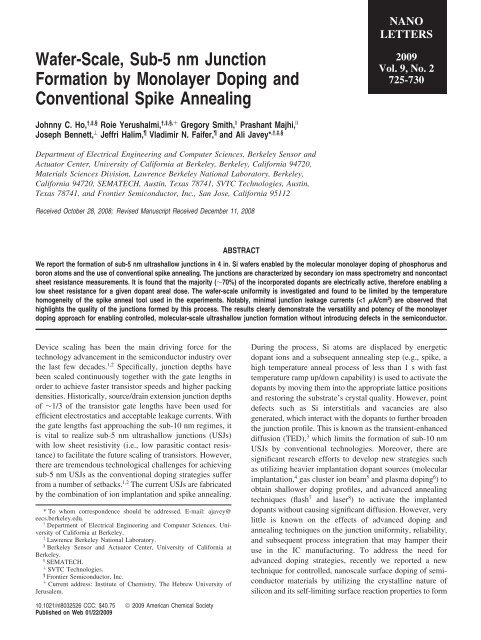
Figure 1. Process schematic for the wafer-scale monolayer doping approach.<br />
self-assembled dopant monolayers followed <strong>by</strong> a subsequent<br />
annealing step for the incorporation <strong>and</strong> diffusion of dopants. 9<br />
Because of the lack of damage to the lattice during this<br />
surface-doping strategy, minimal TED effects are expected<br />
which presents a major advantage of this technology for<br />
achieving nanoscale junctions. Previously, we reported<br />
junction depths down to ∼20 <strong>nm</strong> <strong>by</strong> utilizing the monolayer<br />
doping method <strong>and</strong> 5 s rapid thermal diffusion. 9 Here, we<br />
explore <strong>and</strong> characterize the junction depth limits of this<br />
process on wafer-scale <strong>and</strong> in detail through materials <strong>and</strong><br />
electrical characterizations. Uniquely, for the first time, we<br />
demonstrate sub-5 <strong>nm</strong> junction depths (down to ∼2 <strong>nm</strong>,<br />
which is at the limit of most characterization methods) with<br />
low sheet resistivity, even for fast diffusing dopants such as<br />
phosphorus.<br />
The monolayer doping (MLD) process is based on the<br />
formation of self-assembled dopant-containing monolayer on<br />
the crystalline silicon surfaces, followed <strong>by</strong> the subsequent<br />
diffusion of dopants from the surface into the lattice <strong>by</strong> a<br />
thermal annealing step (Figure 1). In detail, for the phosphorus-<br />
MLD (P-MLD) process, 4 in. p-type Si wafers were first<br />
treated with dilute hydrofluoric acid (∼1%) to remove the<br />
native SiO 2 . The Si surface was then reacted with diethyl<br />
1-propylphosphonate (DPP, Alfa Aesar) <strong>and</strong> mesitylene as<br />
a solvent (25:1, v/v) for 2.5 h at 120 °C to assemble a<br />
P-containing monolayer. The details of this reaction <strong>and</strong> the<br />
monolayer formation kinetics have been reported elsewhere.<br />
9,10 Then, a layer of ∼50 <strong>nm</strong> thick SiO 2 is electronbeam<br />
evaporated as a cap, <strong>and</strong> the substrate is spike annealed<br />
between 900-1050 °C in Ar ambient to drive in the P atoms<br />
<strong>and</strong> achieve n + /p USJs. The spike annealing is performed in<br />
a rapid thermal processing tool (AG Associate, model 610)<br />
with a fast ramping rate of 100 °C/s to the target temperature.<br />
During the annealing, the 4 in. Si wafer is placed on top of<br />
a 6 in. pocket wafer <strong>and</strong> temperature is monitored <strong>by</strong> the<br />
pyrometer controlling system. A similar approach was<br />
applied to 4 in. n-type Si wafers for boron-MLD (B-MLD)<br />
for which hydrogen-terminated Si wafers were reacted with<br />
allylboronic acid pinacol ester (ABAPE, Aldrich) <strong>and</strong><br />
mesitylene as a solvent (25:1, v/v) at 120 °C for 2.5 h to<br />
enable a B-containing monolayer that is then capped with<br />
SiO 2 followed <strong>by</strong> spike anneal to enable the formation of<br />
p + /n USJs. 9 Finally, the oxide cap is removed <strong>and</strong> the enabled<br />
junctions are characterized.<br />
Secondary ion mass spectrometry (SIMS) measurements<br />
were performed to characterize the dopant profiles. Figure<br />
2A illustrates the phosphorus SIMS profiling for P-MLD with<br />
spike anneal temperatures of 950-1050 °C. Notably, for all<br />
samples there is a dramatic change in the P profile at the<br />
concentration of 1∼5 × 10 19 atoms/cm 3 , which is known as<br />
the “kink-<strong>and</strong>-tail” characteristic. This behavior has been<br />
commonly observed for the conventional phosphorus doping<br />
schemes 11 <strong>and</strong> is attributed to the changeover from the<br />
vacancy-assisted diffusion mechanism (at high P concentration<br />
region) to the kick-out diffusion mechanism (at low P<br />
concentration region). 12 From the temperature dependency,<br />
two trends are clearly evident. First, the surface concentration<br />
of incorporated P monotonically increases with the annealing<br />
temperature (Figure 2B). Specifically, surface doping concentrations<br />
of N o ∼ 2.5 × 10 20 , 3.5 × 10 20 ,4× 10 20 , 5.5 ×<br />
10 20 atoms/cm 3 are observed for 900, 950, 1000, 1050 °C,<br />
respectively. This trend is consistent with the constant source,<br />
surface diffusion model, in which N o is governed <strong>by</strong> the<br />
dopant solubility limit at the diffusion temperature. In fact,<br />
the observed temperature dependency of N o is in close<br />
agreement with the previously reported solid solubility limits<br />
(Figure 2B). 13,14 In the MLD process, the maximum areal<br />
dose, Q, corresponds to the monolayer packing density (∼8<br />
× 10 14 molecules/cm 2 assuming a molecular footprint of<br />
∼0.12 <strong>nm</strong> 2 ); hence, at a first glance, it may seem that the<br />
limited source diffusion model is more applicable. However,<br />
in this work, since spike annealing is applied, the monolayer<br />
packing density is higher than the areal dose of the<br />
incorporated/diffused dopants. Therefore, within the context<br />
of this work, constant source model may be applied as a<br />
rough guideline in predicting the doping profile behaviors.<br />
The second clear trend observed from the SIMS profiling<br />
is a monotonic increase in the junction depth <strong>and</strong> areal dopant<br />
726 Nano Lett., Vol. 9, No. 2, 2009
Figure 2. Phosphorus monolayer doping characterization. (A)<br />
Secondary ion mass spectrometry (SIMS) profile of phosphorus<br />
atoms for different spike anneal temperatures. (B) Phosphorus<br />
surface concentration, N o obtained from SIMS analysis for MLDprocessed<br />
samples as a function of spike annealing temperature.<br />
For comparison, the previously reported solid-solubility limits for<br />
different temperatures are also shown. (C) Phosphorus areal dose<br />
vs junction depth (at a background of 5 × 10 18 atoms/cm 3 ) for<br />
different spike anneal temperatures.<br />
Figure 3. Noncontact R s <strong>and</strong> junction leakage current measurement<br />
schematic.<br />
dose with the diffusion temperature. The junction depth, x j<br />
is defined as the depth at which the incorporated P<br />
concentration equates the background B concentration of the<br />
substrate (∼5 × 10 18 B atoms/cm 3 ), while Q is extracted <strong>by</strong><br />
integrating the total area of the dopant profiles. Notably, the<br />
substrate concentration of 5 × 10 18 atoms/cm 3 used here is<br />
the same as the channel doping density for the state-of-the<br />
art Si MOSFETs. We extract x j ∼ 2, 5, 7, 25 <strong>nm</strong> <strong>and</strong> Q ∼<br />
5.5 × 10 12 , 1.0 × 10 13 , 1.7 × 10 13 , 7.5 × 10 13 P atoms/cm 2<br />
for 900, 950, 1000, 1050 °C spike anneals, respectively<br />
(Figure 2C). This trend is expected <strong>and</strong> arises from the<br />
enhanced diffusivity <strong>and</strong> solubility of P in Si at higher<br />
diffusion temperatures. It should be noted that given the finite<br />
temperature ramp time (∼100 °C/s) of our rapid thermal<br />
annealing tool, the diffusion time is also effectively increased<br />
for the samples treated at higher annealing temperatures,<br />
which may also attribute to the observed temperature<br />
dependency of the dopant dose.<br />
The sub-5 <strong>nm</strong> USJs with high Q enabled <strong>by</strong> MLD are<br />
highly attractive <strong>and</strong> clearly demonstrate the potency <strong>and</strong><br />
viability of this technology for future nanoscale complementary<br />
metal oxide semiconductor (CMOS) fabrication<br />
processing. This unique feature of MLD arises from the lack<br />
of TED during the dopant incorporation, which is in distinct<br />
contrast to the ion implantation process. Additionally, in the<br />
MLD process the incorporated dopant atoms near the surface<br />
are not lost during the SiO 2 cap (i.e., mask) removal step,<br />
owing to the high etch selectivity of the oxide over crystalline<br />
Si. This is in distinct contrast to the ion implantation process<br />
in which the post-implantation mask removal <strong>and</strong> surface<br />
cleaning steps lead to some dopant (<strong>and</strong> Si) loss near the<br />
surface due to the enhanced etch rate <strong>and</strong> reduced etch<br />
selectivity of the damaged (nearly amorphized <strong>by</strong> the<br />
implanted ions) top Si layer. Uniquely, this work shows that<br />
conventional annealing methods can indeed enable sub-5 <strong>nm</strong><br />
USJs when dopants are introduced from the surface, which<br />
is yet another beneficial aspect of MLD since the uniformity<br />
<strong>and</strong> reliability of sub-millisecond, nonequilibrium annealing<br />
methods 7,8 (i.e., flash <strong>and</strong> laser) are still unknown <strong>and</strong> under<br />
active investigation.<br />
While SIMS is highly valuable for obtaining the overall<br />
dopant profiles, some uncertainty <strong>and</strong> error may be expected<br />
in the measured profiles, especially for the first 1-2 <strong>nm</strong> depth<br />
from the surface <strong>and</strong> even when the measurement tool is<br />
cautiously operated near the depth resolution limit (see<br />
Supporting Information). Additionally, SIMS does not<br />
provide information on the electrically active content of the<br />
incorporated dopants, which is critical for the device applications.<br />
Therefore, to further characterize the n + /p USJs<br />
<strong>and</strong> examine the electrically active concentration of the<br />
incorporated dopants, sheet resistance (R s ) measurements are<br />
imperative. However, accurate R s measurements are quite<br />
challenging for USJs. Specifically, conventional contactmode,<br />
four-point probe measurements cannot be utilized for<br />
sub-10 <strong>nm</strong> USJs because of the probe penetration into the<br />
surface of the substrate. 15 This probe penetration causes<br />
significant junction damage <strong>and</strong> leakage which underestimates<br />
the true R s with a corresponding error as high as 100%<br />
or more. 15 In this aspect, we utilized the noncontact R s<br />
technique to electrically characterize our USJs. Briefly, this<br />
method relies on the principle of measuring the difference<br />
in the surface photovoltage between two noncontact, voltage<br />
probes as induced <strong>by</strong> an external light source (Figure 3). By<br />
varying the light modulation frequency, the spatially resolved<br />
surface voltage can yield an accurate estimation of R s <strong>and</strong><br />
Nano Lett., Vol. 9, No. 2, 2009 727
Figure 4. Noncontact sheet resistance (in Ω/0) wafer map for P-MLD samples with spike anneal temperatures of (A) 900, (B) 950, (C)<br />
1000, <strong>and</strong> (D) 1050 °C.<br />
Figure 5. (A) Sheet resistance (in Ω/0) versus x j for phosphorusdoped<br />
Si samples reported in this work (<strong>by</strong> P-MLD) <strong>and</strong> the<br />
literature (<strong>by</strong> conventional doping methods). The dot line shows a<br />
simple constant source diffusion model (see Supporting Information)<br />
for comparison purposes. (B) Dopant activation efficiency for<br />
P-MLD samples as a function of spike annealing temperature.<br />
the junction leakage current density with the details reported<br />
elsewhere. 16 Figure 4 shows the noncontact R s wafer maps<br />
for the n + /p junctions enabled <strong>by</strong> MLD. Average R s ∼<br />
12 000, 3670, 3160, 825 Ω/0 are observed for the 900, 950,<br />
1000 <strong>and</strong> 1050 °C spike anneals, respectively. This temperature<br />
dependency is expected due to the higher diffusivity<br />
<strong>and</strong> solubility of dopants (i.e., higher Q) at higher temperatures,<br />
which effectively results in higher free carrier<br />
concentrations <strong>and</strong> lower R s .<br />
From the wafer-scale R s maps, a modest st<strong>and</strong>ard deviation<br />
of σ e 30% is obtained for all samples, except for the 900<br />
°C spike annealed wafer (Figure 4). The large variation (σ<br />
∼ 100%) in the R s for the 900 °C spike wafer may be due<br />
to the average measured R s ∼12 00 Ω/0 being close to the<br />
resolution limit of the noncontact R s measurement set up.<br />
Notably, clear rotational symmetry is observed in the R s maps<br />
for all samples with R s being highly uniform (σ < 5%) within<br />
each circular “ring” boundaries. This variation pattern is a<br />
signature of the spatial imbalance in the power density of<br />
the heater lamp, 17 which may be expected since the annealing<br />
tool used in this study was not designed for spike anneal<br />
applications. 18 Notably, the ring pattern is off-centered for<br />
the 1050 °C wafer (Figure 4D) because the wafer was<br />
misaligned from the center of the support substrate during<br />
the annealing step, again indicative of the role of the<br />
nonuniform heating in the observed R s variation. Given that<br />
R s is highly uniform within each ring, we speculate that in<br />
the future, a higher uniformity across the wafer may be<br />
attained <strong>by</strong> MLD if a more sophisticated spike annealing<br />
tool is used. This is an expected feature of MLD since the<br />
dopants are deterministically positioned on the surface of<br />
the wafer through a self-limiting monolayer formation<br />
reaction, therefore, providing a high degree of control in the<br />
uniformity of surface dopant coverage prior to the diffusion<br />
step.<br />
In order to compare our P-MLD processed n + /p USJs with<br />
those achieved <strong>by</strong> other doping technologies, we complied<br />
the literature reported R s <strong>and</strong> x j values for phosphorus doped<br />
junctions as depicted in Figure 5A. 19-23 From the literature,<br />
728 Nano Lett., Vol. 9, No. 2, 2009
the smallest x j ∼ 13 <strong>nm</strong> at the background concentration of<br />
5 × 10 18 atoms/cm 3 was reported with R s ∼650 Ω/cm. To<br />
the best of our knowledge, there is no previous report of<br />
sub-10 <strong>nm</strong> n + /p USJs based on the phosphorus diffusion in<br />
part because of the high diffusivity of P, highlighting the<br />
elegance of MLD in achieving nanometer-scale junctions,<br />
even for fast diffusing impurities. Notably, for x j ∼ 25 <strong>nm</strong>,<br />
the R s values obtained from MLD are comparable (within a<br />
factor of ∼2) with those obtained <strong>by</strong> other conventional<br />
doping methods (Figure 5A). Moreover, a simple, analytical<br />
constant-source diffusion modeling (P in Si) was carried out<br />
(Figure 5A) to further shed light on the MLD experimental<br />
data (see Supporting Information for details). The experimental<br />
values qualitatively fit the modeling trend, again<br />
demonstrating the near ideal behavior of the MLD process.<br />
From the SIMS <strong>and</strong> R s measurements, the phosphorus<br />
activation efficiency, η, was directly obtained for each<br />
diffusion temperature (Figure 5B) in order to shed light on<br />
the percentage of the incorporated dopants that are electrically<br />
active. Specifically, R s was estimated from the SIMS<br />
profiles <strong>by</strong> eq 1 <strong>and</strong> then compared to the noncontact R s<br />
measurement values<br />
x j<br />
R -1 s,SIMS )∫ qµ(N)N(x)dx (1)<br />
0<br />
where q, µ, N, <strong>and</strong> x are the elemental charge, electron<br />
mobility, dopant concentration, <strong>and</strong> depth, respectively. The<br />
efficiency is then defined as η ) (R s,SIMS )/(R s,measurement ). Figure<br />
5B shows the extracted efficiencies of η ∼ 70% for spike<br />
annealing temperatures g950 °C with η ∼ 30% for the 900<br />
°C spike anneal. The discrepancy between the measured <strong>and</strong><br />
calculated R s values may be attributed to some percentage<br />
of the diffused dopants that are incorporated in sites other<br />
than substitutional lattice sites. 12 However, since in the MLD<br />
dopants are introduced from the surface <strong>by</strong> an equilibrium<br />
process, we expect the diffusion of dopants to be dominated<br />
<strong>by</strong> the substitutional mechanism, resulting in nearly all the<br />
incorporated dopants being electrically active. Therefore, we<br />
speculate that the small discrepancy between the measured<br />
<strong>and</strong> calculated R s values arise from the uncertainty in the<br />
SIMS profiles. This error is particularly magnified for the<br />
900 °C wafer since the observed junction depth is only ∼2<br />
<strong>nm</strong> for this sample, right at the resolution limit of SIMS.<br />
The high η estimated from the data analysis is yet another<br />
highly attractive feature of MLD since for device applications,<br />
only the electrically active contents are desirable with<br />
other dopants inducing defects <strong>and</strong>/or junction leakage<br />
currents.<br />
Since organic molecular precursors are utilized as the<br />
dopant source, carbon incorporation during the dopant<br />
diffusion may be expected, which may enhance the highly<br />
undesired junction leakage currents. Therefore, investigations<br />
of C incorporation <strong>and</strong> the arising junction properties are<br />
needed. However, SIMS measurements do not provide<br />
accurate C depth profiling near the surface region due to the<br />
atmospheric organic surface contaminants that is unavoidable<br />
even if a premeasurement cleaning step is performed on the<br />
samples. 24 Instead, in order to directly characterize the effect<br />
of potential carbon incorporation, the junction leakage current<br />
density was measured <strong>by</strong> the noncontact, photovoltage<br />
measurement. Figure S3 in Supporting Information illustrates<br />
the leakage current wafer map for the n + /p junctions for<br />
various spike temperatures. The average leakage currents of<br />
∼0.13, 0.55, 0.11, 0.31 µA/cm 2 were measured for the 900,<br />
950, 1000, 1050 °C spike anneals, respectively. Notably, the<br />
small leakage currents (
References<br />
(1) Peercy, P. S. The drive to miniaturization. Nature 2000, 406, 1023–<br />
1026.<br />
(2) Claeys, C. Technological challenges of advanced CMOS processing<br />
<strong>and</strong> their impact on design aspects. 17th International Conference<br />
Proceedings on VLSI Design 2004, 2004, 275–282.<br />
(3) Stolk, P. A.; Gossmann, H. J.; Eaglesham, D. J.; Poate, J. M.<br />
Implantation <strong>and</strong> transient boron diffusion: the role of Si self<br />
interstitials. Nucl. Instrum. Methods Phys. Res., Sect. B 1995, 96, 187.<br />
(4) Kawasaki, Y.; Kuroi, T.; Yamashita, T.; Horita, K.; Hayashi, T.;<br />
Ishibashi, M.; Togawa, M.; Ohno, Y.; Yoneda, M.; Horshy, T.;<br />
Jacobson, D.; Krull, W. Ultra-shallow junction formation <strong>by</strong> B 18 H 22<br />
ion implantation. Nucl. Instrum. Methods Phys. Res., Sect. B 2005,<br />
237, 25–29.<br />
(5) MacCrimmon, R.; Hautala, J.; Gwinn, M.; Sherman, S. Gas cluster<br />
ion beam infusion processing of semiconductors. Nucl. Instrum.<br />
Methods Phys. Res., Sect. B 2006, 242, 427–30.<br />
(6) Yon, G. H.; Buh, G. H.; Park, T.; Hong, S. J.; Shin, Y. G.; Chung,<br />
U.; Moon, J. T. Ultra Shallow <strong>Junction</strong> <strong>Formation</strong> Using Plasma<br />
<strong>Doping</strong> <strong>and</strong> Laser Annealing for <strong>Sub</strong>-65 <strong>nm</strong> Technology Nodes. Jpn.<br />
J. Appl. Phys. 2006, 45, 2961–2964.<br />
(7) Ito, T.; Iinuma, T.; Murakoshi, A.; Akutsu, H.; Suguro, K.; Arikado,<br />
T.; Okumura, K.; Yoshioka, M.; Owada, T.; Imaoka, Y.; Murayama,<br />
H.; Kusuda, T. 10-15 <strong>nm</strong> Ultrashallow <strong>Junction</strong> <strong>Formation</strong> <strong>by</strong> Flash-<br />
Lamp Annealing. Jpn. J. Appl. Phys. 2002, 41, 2394–98.<br />
(8) Poon, C. H.; Cho, B. J.; Lu, Y. F.; Bhat, M.; See, A. Multiple-pulse<br />
laser annealing of preamorphized silicon for ultrashallow boron<br />
junction formation. J. Vac. Sci. Technol., B 2003, 21 (2), 706–709.<br />
(9) Ho, J. C.; Yerushalmi, R.; Jacobson, Z. A.; Fan, Z.; Alley, R. L.;<br />
Javey, A. Controlled nanoscale doping of semiconductors via molecular<br />
monolayers. Nat. Mater. 2008, 7 (1), 62–67.<br />
(10) Yerushalmi, R.; Ho, J. C.; Fan, Z.; Javey, A. Phosphine Oxide<br />
<strong>Monolayer</strong>s on SiO 2 Surfaces. Angew. Chem., Int. Ed. 2008, 47, 4440–<br />
4442.<br />
(11) Bentzen, A.; Schubert, G.; Christensen, J. S.; Svensson, B. G.; Holt,<br />
A. Influence of temperature during phosphorus emitter diffusion from<br />
a spray-on source in multicrystalline silicon solar cell processing. Prog.<br />
PhotoVoltaics 2007, 15, 281–289.<br />
(12) Uematsu, M. Simulation of boron, phosphorus, <strong>and</strong> arsenic diffusion<br />
in silicon based on an integrated diffusion model, <strong>and</strong> the anomalous<br />
phosphorus diffusion mechanism. J. Appl. Phys. 1997, 82-5, 2229.<br />
(13) Trumbore, F. A. Solid Solubilities of Impurity elements in Ge <strong>and</strong> Si.<br />
Bell Syst. Tech. J. 1960, 35, 205.<br />
(14) Borisenko, V. E.; Yudin, S. G. Steady-State Solubilities of <strong>Sub</strong>situtional<br />
Impurities in Si. Phys. Status Solidi A 1987, 1 (101), 123–127.<br />
(15) Clarysse, T.; Vanhaeren, D.; V<strong>and</strong>ervorst, W. Impact of probe<br />
penetration on the electrical characterization of sub-50 <strong>nm</strong> profiles. J.<br />
Vac. Sci. Technol., B 2002, 20 (1), 459–66.<br />
(16) Faifer, V. N.; Current, M. I.; Wong, T. M. H.; Souchkov, V. V.<br />
Noncontact sheet resistance <strong>and</strong> leakage current mapping for ultrashallow<br />
junctions. J. Vac. Sci. Technol., B. 2008, 26 (1), 420–24.<br />
(17) Faifer, V. N.; Current, M. L.; Nguyen, T.; Wong, T. M. H.; Souchkov,<br />
V. V. Non-contact measurement of sheet resistance <strong>and</strong> leakage<br />
current: applications for USJ-SDE/halo junctions. Ext. Abs. of the 5th<br />
IWJT, IEEE 2005, pp45-8.<br />
(18) Since the 4 in. wafer is placed on a support substrate during the spike<br />
annealing (the tool was designed to h<strong>and</strong>le 6 in. wafers), this may<br />
also contribute to the variation pattern.<br />
(19) Collarta, E. J. H.; Felch, S. B.; Pawlak, B. J.; Absil, P. P.; Severi, S.;<br />
Janssens, T.; V<strong>and</strong>ervorst, W. Co-implantation with conventional spike<br />
anneal solutions for 45 <strong>nm</strong> n-type metal-oxide-semiconductor ultrashallow<br />
junction formation. J. Vac. Sci. Technol., B. 2006, 24 (1),<br />
507–9.<br />
(20) Augendre, E.; Pawlak, B. J.; Kubicek, S.; Hoffmann, T.; Chiarella,<br />
T.; Kerner, C.; Severi, S.; Falepin, A.; Ramos, J.; De Keersgieter, A.;<br />
Eyben, P.; Vanhaeren, D.; V<strong>and</strong>ervorst, W.; Jurczak, M.; Absil, P.;<br />
Biesemans, S. Superior N- <strong>and</strong> P-MOSFET scalability using carbon<br />
co-implantation <strong>and</strong> spike annealing. Solid-State Electron. 2007, 51<br />
(11-12), 1432–6.<br />
(21) Lee, S. W.; Jeong, J. Y.; Park, C. S.; Kim, J. H.; Ji, J. Y.; Choi, J. Y.;<br />
Lee, Y. J.; Han, S. H.; Kim, K. M.; LeeW. J.; Rha, S. K.; Oh, J. K.<br />
The study of plasma doping process for ultra shallow junctions. Ext.<br />
Abs. of the 7th IWJT, IEEE 2007, 67-8.<br />
(22) Cagnat, N.; Laviron, C.; Mathiot, D.; R<strong>and</strong>o, C.; Juhel, M. Shallow<br />
<strong>Junction</strong> Engineering <strong>by</strong> Phosphorus <strong>and</strong> Carbon Co-implantation:<br />
Optimization of Carbon Dose <strong>and</strong> Energy. Mater. Res. Soc. Symp.<br />
Proc. 2007, 994, 0994-F08-04.<br />
(23) Pawlak, B. J.; Duffy, R.; Augendre, E.; Severi, S.; Janssens, T.; Absil,<br />
P.; V<strong>and</strong>ervorst, W.; Collart, E.; Felch, S.; Schreutelkamp, R.; Cowern,<br />
N. The Carbon Co-Implant with Spike RTA Solution for Phosphorus<br />
Extension. Mater. Res. Soc. Symp. Proc. 2006, 912, 0912-C01-06.<br />
(24) Beebe, M.; Bennett, J.; Barnett, J.; Berlin, A.; Yoshinaka, T.<br />
Quantifying residual <strong>and</strong> surface carbon using polyencapsulation SIMS.<br />
Appl. Surf. Sci. 2004, 231-32, 716–19.<br />
(25) Chen, J. T. C.; Dimitrova, T.; Dimitrov, D. A New Method for<br />
Mapping Ultra-Shallow <strong>Junction</strong> Leakage Currents. International<br />
Workshop on IWJT, IEEE 2006, 100.<br />
NL8032526<br />
730 Nano Lett., Vol. 9, No. 2, 2009
Supporting Information<br />
<strong>Wafer</strong>-<strong>Scale</strong>, <strong>Sub</strong>-5 <strong>nm</strong> <strong>Junction</strong> <strong>Formation</strong> <strong>by</strong> <strong>Monolayer</strong> <strong>Doping</strong> <strong>and</strong><br />
Conventional Spike Annealing<br />
Johnny C. Ho, 1,2,3 Roie Yerushalmi, 1,2,3,† Gregory Smith, 4 Prashant Majhi, 4 Joseph Bennett, 5 Jeffri Halim, 6<br />
Vladimir N. Faifer, 6 Ali Javey 1,2,3,*<br />
1 Department of Electrical Engineering <strong>and</strong> Computer Sciences, University of California at Berkeley,<br />
Berkeley, CA, 94720, USA.<br />
2 Materials Sciences Division, Lawrence Berkeley National Laboratory, Berkeley, CA 94720, USA.<br />
3 Berkeley Sensor <strong>and</strong> Actuator Center, University of California at Berkeley, Berkeley, CA, 94720, USA.<br />
4 SEMATECH, Austin, TX, 78741, USA.<br />
5 SVTC Technologies, Austin, TX, 78741, USA.<br />
6 Frontier Semiconductor, Inc., San Jose, CA, 95112, USA.<br />
†<br />
Current address: Institute of Chemistry, The Hebrew University of Jerusalem<br />
* Corresponding author: ajavey@eecs.berkeley.edu<br />
S1
Details of SIMS measurements for P profiling<br />
The SIMS measurements reported for the n+/p USJs were performed on the front side of<br />
the samples after the oxide caps were removed in HF. The samples were then etched in st<strong>and</strong>ard<br />
clean solution (SC1, mixture of ammonia hydroxide / hydrogen peroxide / de-ionized water) to<br />
remove organic material before the analyses. The analyses were performed on the Physical<br />
Electronics ADEPT-1010. The P+ 30 Si signal was monitored as negative ions under 500eV Cs +<br />
bombardment incident at 60°. Secondary ions were collected from the center 20% of a 400 µm x<br />
400 µm rastered area. Stylus profilometry was used to determine the depth of the craters <strong>and</strong><br />
calibrate the depth scale. The P concentration was calculated using a relative sensitivity factor<br />
(RSF) determined from a st<strong>and</strong>ard sample. Importantly, the SC1 clean effectively removed the<br />
organic contamination that was interfering with the P signal. We noted that the SCI clean<br />
oxidized the Si surface but would not affect the SIMS measurement. The profiles obtained after<br />
the cleaning give a much valid representation of the P distribution.<br />
SIMS measurements for front-side depth profiling of P thru the oxide cap were also<br />
performed but the organic monolayer induces an additional sample charging just beyond the<br />
oxide/Si interface <strong>and</strong> this interference distorts the signals collected <strong>and</strong> makes the profiles<br />
invalid. Moreover, backside SIMS measurements were carried out as well; however, backside<br />
profiling requires the sample thinning down to 100<strong>nm</strong> in which imposes a huge technical<br />
challenge to obtain reliable profiles in USJs.<br />
S2
Boron MLD<br />
10 20<br />
A<br />
1050 0 C<br />
950 0 C<br />
[B] (atoms/cm 3 )<br />
10 19<br />
10 18<br />
<strong>Junction</strong> background<br />
concentration<br />
10 17<br />
2<br />
4 6<br />
Depth (<strong>nm</strong>)<br />
8<br />
10<br />
1.2x10 12<br />
B<br />
3.0<br />
Dose (atoms/cm 2 )<br />
1.0<br />
0.8<br />
0.6<br />
2.5<br />
2.0<br />
1.5<br />
x j<br />
(<strong>nm</strong>)<br />
0.4<br />
950 1000 1050<br />
Anneal Temperature ( o C)<br />
1.0<br />
Figure S1. Boron monolayer doping characterization. A. Secondary Ion Mass Spectrometry (SIMS)<br />
profile of boron for different spike anneal temperatures. B. SIMS extracted boron dose versus junction<br />
depth (at a background of 5x10 18<br />
atoms/cm 3 ) for different spike anneal temperatures.<br />
S3
In addition to the n+/p junctions, we also investigate the formation of p+/n USJs <strong>by</strong><br />
boron-MLD with spike annealing. Figure S1 shows the SIMS profiles of diffused boron atoms in<br />
the junctions for both 950 <strong>and</strong> 1050 o C spike. The profiles decrease sharply from low 10 19 cm-3<br />
on the surface to the junction. We extracted x j ~1.5, 2.1 <strong>nm</strong> <strong>and</strong> Q~5.3x10 11 , 9.7x10 11<br />
B<br />
aomts/cm 2 for 950, 1050ºC spike anneals, respectively (Fig. S1B). This trend is expected <strong>and</strong><br />
arises from the enhanced diffusivity <strong>and</strong> solubility of B in Si at higher diffusion temperatures.<br />
We note that the SIMS profiles <strong>and</strong> junction depths attained here are at the resolution limit of<br />
SIMS analysis which may create some uncertainties in the exact accuracy of the profiles.<br />
The SIMS measurements here were done similar to the ones of n+/p USJs. Front-side<br />
depth profiling of B was performed after the oxide caps were removed in HF. The analyses were<br />
carried out in the Physical Electronics ADEPT-1010. The 11 B signal was monitored as a positive<br />
ion under 650eV O + 2 bombardment incident at 45°. The analysis chamber was backfilled with a<br />
high partial pressure of O 2 to reduce ion yield variations at the beginning of the profile.<br />
Secondary ions were collected from the center 20% of a 400 µm x 400 µm rastered area. Stylus<br />
profilometry was used to determine the depth of the craters <strong>and</strong> calibrate the depth scale. The B<br />
concentration was calculated using a relative sensitivity factor (RSF) determined from a st<strong>and</strong>ard<br />
sample. Again, both front-side profiling thru the oxide cap <strong>and</strong> back-side profiling were also<br />
explored but same challenges came up similar to the ones of n+/p USJs.<br />
S4
Activation efficicency (η) calculations<br />
From SIMS profiles, assuming all the dopants are fully activated, the R s,SIMS can be<br />
estimated <strong>by</strong> dividing the profile into many thin slabs. Each R s,slab can be calculated as the<br />
Equation S1 S1 ,<br />
ρ 1<br />
=<br />
x qN<br />
R s , slab<br />
= µ<br />
x<br />
Eq. S1<br />
R<br />
s,<br />
slab<br />
ρ<br />
= =<br />
x ⎡<br />
⎢<br />
qN ⎢µ<br />
⎢<br />
⎢⎣<br />
min<br />
1<br />
µ<br />
max<br />
− µ<br />
N<br />
(1 + )<br />
N<br />
r<br />
min<br />
α<br />
⎤<br />
⎥<br />
⎥x<br />
⎥<br />
⎥⎦<br />
Phosphorous<br />
µ min (cm 2 /Vs) 68.5<br />
µ max (cm 2 /Vs) 1414<br />
N r (cm -3 ) 9.20x10 16<br />
α 0.711<br />
where ρ, x, q, N <strong>and</strong> µ are the resistivity, thickness, elemental charge, dopant concentration,<br />
carrier mobility of the slab, respectively. The R s,SIMS can be found <strong>by</strong> summing all the resistance<br />
1 1<br />
of the slabs, = ∑ . This R s , SIMS can then be compared to the measured R s in order to<br />
R<br />
s,<br />
SIMS<br />
Rs,<br />
slab<br />
Rs,<br />
SIMS<br />
determine the activation efficiency, η = .<br />
R<br />
s,<br />
measurement<br />
For example, R s,SIMS was determined to be ~600 Ω/□ from the SIMS profile of the n+/p<br />
1050 o C spike anneal. Also, R s,measurement was found to be ~850 Ω/□ in the corresponding SIMS<br />
600<br />
measured region. This way, the activation efficiency can be estimated as ~71%, η = = 71% .<br />
850<br />
S5
Analytical constant-source diffusion modeling (P in Si)<br />
[P] (atoms/cm 3 )<br />
10 21<br />
10 20<br />
10 19<br />
background<br />
concentration<br />
t=0.5s<br />
t=10s<br />
t=100s<br />
t=500s<br />
t=2000s<br />
t=4000s<br />
x j<br />
10 18<br />
0<br />
20 40 60<br />
Depth (<strong>nm</strong>)<br />
80<br />
Figure S2. Phosphorus profile of the constant-source diffusion model (N o ~3x10 20 cm -3 <strong>and</strong> D~8x10 16 cm 2<br />
s -1 ).<br />
N(<br />
x,<br />
t)<br />
= N<br />
For the constant-source diffusion, the dopant profile can be determined <strong>by</strong> the equation,<br />
o<br />
x<br />
erfc(<br />
) , where N o , D <strong>and</strong> erfc are the surface concentration, diffusion<br />
2 Dt<br />
coefficient <strong>and</strong> complementary error function, respectively. For example, Figure S2 illustrates<br />
the modeled profile for the phosphorus diffusion in silicon at 900 o C for increasing diffusion time<br />
with the surface concentration (N o ) of ~3x10 20 cm -3<br />
<strong>and</strong> the diffusion coefficient (D) of<br />
~8x10 16 cm 2 s -1 . Each corresponding junction depth, x j , can be determined at the baseline of the<br />
background concentration as 5x10 18 atoms/cm 3 . Then the sheet resistance, R s , of each x j , can be<br />
calculated using the Equation S1. As a result, the correlation between the R s versus x j for the<br />
constant-source diffusion model can be obtained.<br />
S6
Non Contact <strong>Junction</strong> Leakage Measurements<br />
A<br />
900 o C<br />
Spike<br />
B<br />
950 o C<br />
Spike<br />
10 mm<br />
0.10<br />
0.19<br />
0.28<br />
0.36<br />
0.45<br />
0.54<br />
0.63<br />
0.71<br />
0.80<br />
10 mm<br />
0.10<br />
0.28<br />
0.55<br />
0.83<br />
0.1<br />
1.4<br />
1.6<br />
1.9<br />
2.2<br />
C<br />
10 mm<br />
1000 o C<br />
Spike<br />
0.10<br />
0.14<br />
0.19<br />
0.23<br />
0.28<br />
0.32<br />
0.26<br />
0.41<br />
0.45<br />
D<br />
10 mm<br />
1050 o C<br />
Spike<br />
0.10<br />
0.24<br />
0.38<br />
0.51<br />
0.65<br />
0.79<br />
0.92<br />
1.1<br />
1.2<br />
Figure S3. Non-contact junction leakage (in µA/cm 2 ) wafer mapping for P-MLD samples with<br />
spike anneal temperatures of (A) 900 0 C, (B) 950 0 C, (C) 1000 0 C <strong>and</strong> (D) 1050 0 C.<br />
S7
Reference<br />
S1. Zeghbroeck, B. V. Principles of Semiconductor Devices, 2004 (University of Colorado,<br />
http://ece-www.colorado.edu/~bart/book/book).<br />
S8