Independent Research Study â Final Report - Saket Vora
Independent Research Study â Final Report - Saket Vora
Independent Research Study â Final Report - Saket Vora
You also want an ePaper? Increase the reach of your titles
YUMPU automatically turns print PDFs into web optimized ePapers that Google loves.
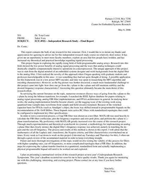
Partners I 2310, Box 7256<br />
Raleigh, NC 27695<br />
Center for Embedded Systems <strong>Research</strong><br />
May 8, 2006<br />
TO:<br />
FROM:<br />
SUBJECT:<br />
Dr. Tom Conte<br />
<strong>Saket</strong> <strong>Vora</strong><br />
ECE 492G – <strong>Independent</strong> <strong>Research</strong> <strong>Study</strong> – <strong>Final</strong> <strong>Report</strong><br />
Dr. Conte,<br />
This report contains the bulk of my research for this semester. First, I would like to re-iterate my thanks and<br />
appreciation for agreeing to advise me for this independent research study course on relatively short notice. It has<br />
given me an opportunity to meet more faculty members, explore an area that few people have trodden, and has<br />
increased my theoretical and practical knowledge regarding signal processing.<br />
This project began in exploring the rapidly rising field of field-programmable analog arrays. <strong>Research</strong> into this<br />
field showed the low power benefits of analog signal processing and the ways that analog techniques could<br />
drastically simplify computationally intensive operations in a microprocessor. The unique approach of this project<br />
was to start from the digital mindset of an embedded systems designer and work backgrounds from the digital filter<br />
to the analog filter. I first realized the novelty of this approach when I began speaking with graduate students and<br />
professors knowledgeable in this area – it was something they had not quite thought of doing. A possible application<br />
for this framework was in a low power MP3 encoder, and time was spent in researching the MP3 algorithm and<br />
encoding characteristics. However, as the big picture was further discussed, a much more fundamental challenge to<br />
this project came into light: how does one go from the z-plane to the s-plane and still maintain stability and the<br />
desired frequency response characteristics Answering this question ultimately became the main thrust of this<br />
research effort.<br />
In surveying the current literature on the topic, numerous resources discuss ways of going from the s-plane to the<br />
z-plane by using the bilinear transform, for example. I searched the IEEE Xplore database for papers relating to<br />
analog signal processing, analog FIR filter implementations, and FPAA architectures in general. In studying these<br />
works, the analog implementation benefits became clearer, yet the nagging issue of the existing work using<br />
quantized time (sample-data waveforms from sample-and-hold circuits) remained. Because of the switchedcapacitor<br />
basis for FPAAs (such as Anadigm’s chips), the focus was shifted instead to programmable biquads on the<br />
recommendation of Dr. Griff Bilbro. These biquads were active RC filters with standardized topologies that could<br />
be configured to implement key filter specifications.<br />
In order to test a conversion process, a 4-tap FIR filter was chosen as a test filter. MATLAB was used heavily to<br />
calculate the FIR filter coefficients, plot the frequency responses and zero-pole plots, and perform the s-plane to z-<br />
plane transformations. My proficiency with MATLAB greatly increased over the course of this research project.<br />
Through much experimentation and theoretical scratchwork in a journal, a methodology for implementing an analog<br />
s-plane filter that closely mimics the digital filter’s frequency response was achieved, namely in matching the dcgain<br />
and the cut-off frequency. The process and results of this method is shown in this report. I will admit that the<br />
mathematics of all the Laplace and z transforms, the Nyquist criteria, and filter characteristics overwhelmed me at<br />
times. Every week as I sat down to work on this project (I devoted my Tuesdays and Thursdays for this), I often ran<br />
through a quick review of the accumulated material in order to keep everything straight.<br />
Future and more thorough investigations of this topic would involve testing the validity of this process for filters<br />
with higher sampling rates, cut-off frequencies, or more complicated topologies than a FIR filter. In addition, the<br />
steps for expressing the s-plane transfer function in a quantized, standardized form and actually implementing a<br />
physical programmable biquad still need to be worked out and explored.<br />
I plan on presenting a summarized version of this research project at next year’s Undergraduate <strong>Research</strong><br />
Symposium. This year’s deadline occurred too soon for me to have quality results. Thank you again for mentoring<br />
me with this challenging, interesting, and exciting project. Please contact me at any time if you have further<br />
questions.<br />
Sincerely,<br />
<strong>Saket</strong> <strong>Vora</strong>
Process for a Programmable Analog Adaptive Filter from<br />
Digital Tap Coefficients<br />
By <strong>Saket</strong> <strong>Vora</strong><br />
Abstract— This paper presents a process for programming a truly continuous time analog<br />
adaptive filter beginning with digital tap coefficients, such as those used in digital signal<br />
processing methods. The motivation is to enable embedded systems to, in essence, ‘compile’<br />
code written for a DSP framework and implement it in an analog filter design, thereby<br />
decreasing the power consumption of the filtering process. The method used in the proposed<br />
process involves mapping the digital filter’s poles and zeros in the z-plane to an ideal analog<br />
filter’s s-plane and ensuring an acceptable frequency response. A programmable bi-quad is<br />
proposed for implementing the analog filter.<br />
Index Terms— analog signal processing, z-plane to s-plane mapping, tap coefficients, embedded systems filtering<br />
I. INTRODUCTION<br />
FOR years digital filters have dominated the field of signal processing due to their high degree<br />
of programmability and maintaining accuracy. Analog filters were time-consuming to design and<br />
fabricate while offering almost no re-programmability. In addition, process variations and nonideal<br />
physical environments would degrade their accuracy. However, modern processes have<br />
improved significantly to make analog circuits robust and able to maintain approximately 10 bits<br />
of accuracy. Techniques such as programmable bi-quads and recently field programmable analog<br />
arrays have introduced the idea of practical re-programmability to analog circuits and filters [1-<br />
7].<br />
2
With the greater emphasis on improving the longevity of portable electronics, low power<br />
consumption is becoming increasingly more important. Analog filters can feature dramatically<br />
improved power consumption characteristics compared to their digital peers because operations<br />
that require repeated intensive computation by the digital signal processor are not required in an<br />
analog setting[2]. In [8]-[10], methods are discussed in implementing FIR filters using analog<br />
techniques.<br />
Switched-capacitors have been a preferred method for implementing FPAAs and features good<br />
accuracy. However, switched-capacitor circuits have higher noise and offset voltage than passive<br />
or active filters[11]. In addition, they are analog in magnitude and quantized in time, due to the<br />
sample-and-hold method utilized. This sampled-data signal allows switched-capacitor based<br />
FPAAs to utilize a digital filtering mindset, with z-transforms and delays. Multiple clock lines at<br />
different frequencies are required for such an FPAA, and the many switches degrade<br />
performance[1].<br />
True continuous time transfer functions are realized from the poles and zeros on the s-plane. In<br />
converting an existing digital filter, one method is to begin with the desired analog specifications<br />
and design the filter using standardized active filter topologies and transfer functions. Once an s-<br />
plane transfer function is determined it can be realized with, for instance, a programmable<br />
biquad[6]. However, this case-by-case conversion process in impractical when quick reprogrammability<br />
is required or in a high speed adaptive filtering implementation.<br />
II. PROPOSED PROCESS FOR DETERMINING ANALOG TRANSFER FUNCTION<br />
A. Process Outline<br />
A process is proposed that will take a digital filter (such as a FIR filter, in this case) in the form<br />
of its tap coefficients and calculate the analog s-plane transfer function. This transfer function,<br />
3
when expressed in a quantized and standardized topology, can then be implemented using a<br />
programmable biquad. There are numerous standardized active RC filter topologies for low pass,<br />
high pass, band pass, and band stop filters. A bank of resistors and capacitors with a cross-bar<br />
network interface with the biquad’s amplifiers would be available to physically implement the s-<br />
domain transfer function. The microprocessor would send digital words to the biquad that when<br />
decoded would close the appropriate crossbar switches necessary to implement the determined<br />
transfer function with the proper topology. Because a crossbar connected bank of resistors and<br />
capacitors can provide a discrete number of possible values, the ideal zero and pole locations will<br />
have to be quantized to what the programmable biquad can physically implement.<br />
Such a process would allow embedded system designers to continue to work in a digital<br />
mindset but ultimately realize the low-power benefits of analog signal processing. In an adaptive<br />
setting, the output of the analog filter would be sampled with an A/D converter and checked by<br />
the microprocessor for desirable characteristics. If an adjustment is required, such as the<br />
appearance of high frequency noise that must be attenuated, the microprocessor will compute<br />
new tap coefficients. These updated coefficients are converted through the process then<br />
downloaded to the analog filter. Figure 1 depicts a flow chart for the proposed process.<br />
4
Digital Filter<br />
Tap Coefficients<br />
Determined<br />
Find zeros<br />
of digital filter<br />
Signal path for<br />
adaptive setting<br />
Convert zeros<br />
to s-plane<br />
Determine location<br />
of s-plane poles<br />
ADC<br />
Convert to<br />
standardized<br />
topology<br />
Quantize values to<br />
available R’s and C’s<br />
Download to<br />
programmable<br />
biquad<br />
Filter Output Resumes<br />
Figure 1 – Process flow chart<br />
At the core of the conversion process, poles and zeros in the z-plane of the digital filter must<br />
be mapped onto the s-plane for the analog filter. Discussion of s-plane to z-plane mapping can be<br />
found in nearly every signal processing textbook. Mapping in the other direction, however, is<br />
not. The first part of this research endeavor involved studying the relationship between the z-<br />
5
plane and the s-plane.<br />
Applying a Laplace transform to a signal sampled at T is shown below [12] :<br />
∞<br />
*<br />
−kTs<br />
X ( s) x( kT ) e<br />
= ∑<br />
k = 0<br />
Substituting<br />
z<br />
sT<br />
= e results in the definition of the one-sided z-transform.<br />
∞<br />
X ( z) = ∑ x( k)<br />
z<br />
k = 0<br />
−k<br />
The exact relationship between the complex variables s and z is<br />
1 s = ln( z)<br />
.<br />
T<br />
The conformal mappings of the s-plane to the z-plane and vice-versa were plotted using this<br />
relationship using MATLAB. An array of points in each plane was taken and transformed. The<br />
mapping was colorized to aid in depicting where the transformed points lie on the<br />
complementary plane. A sampling frequency ω<br />
s<br />
of 8 rad/sec was used.<br />
6
Figure 2 – A radial distribution of points on the z-plane. The unit circle is denoted with the blue line.<br />
Figure 3 – The z-plane points in Figure 2 mapped onto the s-plane. The jω-axis is denoted with the blue line.<br />
This mapping is consistent with the known stability characteristics of the z-plane and the s-plane.<br />
A discrete-time impulse response is stable if all its poles are located inside the unit circle in the z-<br />
plane. A continuous-time impulse response if all its poles are located in the left half of the s-<br />
plane, or has a real component of less than 0. The yellow and red points in Figure 2 map to the<br />
right half side of the s-plane, and the cyan and blue points in Figure 2 map to the left half side of<br />
the s-plane. Also, the mapping on the s-plane extends to ±j4. Because of the sampling, the points<br />
on the unit circle with an angle of ±π translate to<br />
sampling.<br />
j ω s<br />
± . This satisfies the Nyquist criteria for<br />
2<br />
Using this knowledge of z-plane to s-plane mapping, an example conversion is demonstrated<br />
7
with a digital filter.<br />
III. EXAMPLE TRANSFORMATION: 4-TAP FIR FILTER<br />
To demonstrate the transformation process of a digital filter to an analog filter, a 4-tap (thirdorder)<br />
FIR filter was designed with a specified cut-off frequency of 1.25 rad/sec. A FIR filter has<br />
the following transfer function:<br />
3 2<br />
a0z + a1z + a2z + a3<br />
H ( z)<br />
= , or alternatively<br />
3<br />
z<br />
H ( z)<br />
= a + a z + a z + a z .<br />
−1 −2 −3<br />
0 1 2 3<br />
The tap-coefficients for this filter are a 0 , a 1 , a 2 , and a 3 . MATLAB was used to generate the<br />
coefficients for this low-pass FIR filter using the fir1(n,W n ) command, with n being the<br />
order and W n being the normalized cut-off frequency. The tap coefficients were<br />
[a 0 a 1 a 2 a 3 ] = [0.0449 0.4551 0.4551 0.0449]. A zero-pole plot of the z-plane and frequency<br />
response of the FIR filter is shown below.<br />
Figure 4 – A zero-pole plot of the FIR filter in the z-plane.<br />
8
Figure 5 – Frequency response of the FIR filter.<br />
The -3.01 dB and cut-off frequency denoted with dashed lines.<br />
The zeros of the FIR filter were mapped onto the s-plane using the<br />
1 s = ln( z)<br />
relationship<br />
T<br />
described in section II, for a sampling frequency of 8 rad/sec. A FIR filter is always causal, for<br />
all of its poles lie at the origin of the z-plane. This presents an interesting transformation<br />
problem, because the origin of the z-plane is mapped to the negative infinity on the real axis of<br />
the s-plane. Not only is such a pole location impractical to physically implement, it alters the<br />
magnitude of the s-plane analog frequency response. The magnitude of the frequency response is<br />
H ( j )<br />
z<br />
ω = ∏ ∏ p<br />
vectors<br />
vectors<br />
, where z vectors is the product of the vectors from each zero to the jω-axis and<br />
p vectors is the product of the vectors from each pole to the jω-axis for a given ω. If the poles are<br />
located at negative infinity on the real axis, then the magnitude response would approach 0 for<br />
all ω. The s-plane zeros are shown in the figure below.<br />
9
Figure 6 – Plot of the mapped zeros on the s-plane.<br />
An optimal location for the poles can be determined using the location of the s-plane zeros, the<br />
desired cut-off frequency, and the dc magnitude of the frequency response.<br />
The cut-off frequency is that frequency at which the magnitude decreases by approximately,<br />
3.01dB, which is 0.7071 in pure magnitude. For the example filter,<br />
∏<br />
∏<br />
zvectors<br />
H ( j1.25) = = 0.7071.<br />
p<br />
vectors<br />
The mapped zeros are located at ±2.8 + j4 and j4.<br />
2 2<br />
( ) 2<br />
2.8 + (2.75) ⋅ 2.75<br />
42.3569<br />
H ( j1.25) = = = 0.7071<br />
p<br />
p<br />
∏<br />
p<br />
vectors<br />
∏<br />
vectors<br />
42.3569<br />
= = 59.8997<br />
0.7071<br />
∏<br />
vectors<br />
All poles will be located at the same location, thus each pole vector is equivalent. The length of<br />
the pole vector from the j1.25 point is then<br />
p = 3<br />
59.8997 = 3.91268. Thus, in order to meet<br />
vector<br />
the desired cut-off frequency, the location of the poles must lie on a circle with radius 3.91268<br />
with center point j1.25.<br />
10
The digital filter’s frequency response had a dc magnitude of 0 dB, which is 1 in pure<br />
magnitude.<br />
2 2<br />
( ) 2<br />
∏<br />
∏ ∏ ∏<br />
z 2.8 + 4 ⋅ 4<br />
vectors<br />
95.36<br />
H ( j0) = = = = 1 ∴ ∏ pvectors<br />
= 95.36<br />
p p p<br />
vectors vectors vectors<br />
When all the poles are located at the same point, the length of the pole vector is<br />
p = 3<br />
95.36 = 4.569 . In order for the dc magnitude of the analog filter to be 1, the pole<br />
vector<br />
vector must be at a radius of 4.569 from the origin.<br />
These two conditions, the cut-off frequency and the dc gain, each define a circle on the s-plane.<br />
The point that satisfies both conditions is where the two circles intersect. Figure 7 depicts these<br />
conditions graphically.<br />
Figure 7 – The cut-off frequency (red dashed line) and dc gain (blue dashed line)<br />
conditions that the pole location must meet.<br />
The intersection of these two circles for our example filter is the point -3.57039 + j2.85043.<br />
11
When three poles are located at this critical point, the frequency response of the analog filter will<br />
closely approximate the digital filter’s frequency response. A key difference will of course be<br />
that the analog filter is valid from 0 rad/s to<br />
ωs<br />
rad/s, while the digital filter will operate from 0<br />
2<br />
rad/s to π rad/s. The frequency response of the calculated s-plane zeros and poles is shown<br />
overlaid in the figure below with the frequency response of the digital filter.<br />
Figure 8 – The frequency response of the analog filter (in red)<br />
and the frequency response of the digital filter (in blue).<br />
-3.01dB is marked with dashed line.<br />
As Figure 8 shows, the frequency response of the calculated analog filter closely matches that<br />
of the digital filter up to approximately 1.5 rad/s, which is beyond the cut-off frequency.<br />
An alternative approach that was tested involved adjusting the poles of the z-domain transfer<br />
function to be slightly off the origin, such as 0.001 away. However, this resulted in the s-plane<br />
poles to be located very close to the real axis far into the left-half plane, causing too rapid a drop<br />
12
off in magnitude for the frequency response. The cut-off frequency of this alternative stayed<br />
around 0.5 rad/s, well below the specified cut-off frequency of 1.25 rad/s. Determining a new<br />
optimal location for the poles using the method described above is possible in the microprocessor<br />
and results in a more feasible value to physically implement.<br />
IV. FUTURE EXPLORATION<br />
The work presented in section III is for an FIR filter with a small number of taps and<br />
relatively low cutoff and sampling frequencies. This was done to aid in initially exploring the<br />
transformation process. Further investigation should be undertaken to judge the validity of the<br />
proposed method for higher cutoff and sampling frequencies and FIR filters with a greater<br />
number of taps. As the sampling frequency increases, the distribution of zeros and poles on the s-<br />
plane can become more spread out, and so with a given bank of resistors and capacitors there is<br />
conceivably a limit as to the possible cutoff frequencies that can be implemented.<br />
In addition, the latter processes of the proposed method, such as representing the s-plane<br />
transfer function in standardized active circuit topologies with quantized values, such as those<br />
found in [13-14,16], have not yet been addressed.<br />
V. CONCLUSIONS<br />
The motivation for this project was to explore a novel way of enabling embedded system<br />
designers to take advantage of the benefits offered by true analog signal processing while<br />
utilizing existing DSP code and remaining in the digital state of mind. Instead of the quantized<br />
time nature of switched-capacitor circuits, this method is truly analog in both time and<br />
magnitude.<br />
13
REFERENCES<br />
[1] P. Hasler, D. Anderson et al, “Large-Scale Field-Programmable Analog Arrays for Analog<br />
Signal Processing,” IEEE Circuits Syst 1, Reg. Papers, vol 52, no. 11, November 2005.<br />
[2] J. L. Huertas, D. Vazquez, A. Rueda, “Concurrent Testing of Analog Filters Using a<br />
Programmable Biquad”. 1992.<br />
[3] D.R. D’Mello, P.G. Gulak, “Design Approaches to Field-Programmable Analog Integrated<br />
Circuits”. Analog Integrated Circuits and Signal Processing, 17, 7-34 (1998). Kluwer<br />
Academic Publishers, Boston.<br />
[4] P. Hasler, “Low Power Programmable Signal Processing,” Proceedings of the 9 th Int’l<br />
Database Engineering & Application Symposium 2005.<br />
[5] Y. P. Tsividis, D. Vallancourt, “A Fully Programmable Sampled-Data Analog CMOS Filter<br />
with Transfer-Function Coefficients Determined by Timing”, IEEE Journal of Solid-State<br />
Circuits, Vol. SC-22, No. 6, December 1987.<br />
[6] M. B. Halima, M. Fakhfahk, and M. Loulou, “A Switched Current Based FPAA Macrocell<br />
for Mixed Mode Signal Processing Systems”, IEEE Workshop on Signal Processing Systems<br />
Design and Implementation. 2-4 Nov. 2005, pgs 143-147.<br />
[7] J. L. Huertas, A. Rueda, D. Vazquez, “Testable Switched-Capacitor Filters”, IEEE Journal of<br />
Solid State Circuits, Vol. 28, No. 7, July 1993.<br />
[8] P. Hasler, G. Rosen, V. Srinivasan, “Low-Power Realization of FIR Filters Using Current-<br />
Mode Analog-Design Techniques,” 2005.<br />
[9] Z. Ciota, A. Napieralski, J. L. Noullet, “Analogue realization of integrated FIR filters”, IEEE<br />
Proc-Circuit Devices Syst, Vol 143.No.5, October 1996.<br />
14
[10] F.A. Farag, C. Galup-Montoro, and M. C. Schneider, “Digital Programmable Switched-<br />
Current FIR Filter for Low-Voltage Applications”, IEEE Journal of Solid-State Circuits, Vol.<br />
35, No. 4., April 2000.<br />
[11] Lacanette, Kerry. “A Basic Introduction to Filters – Active, Passive, and Switched-<br />
Capacitor”. National Semiconductor, Application Note 779. © April 1991.<br />
[12] Nyack, Cuthbert A. “Z-Transform and Laplace Transform”. Date of Publication: 1996.<br />
Date of Access: February-May, 2006.<br />
<br />
Books<br />
[13] Deliyannis, T., Yichuang, Sun., and Fidler, J.K. “Continuous-Time Active Filter Design”.<br />
CRC Press; New York, NY. © 1999.<br />
[14] Ghausi, Mohammed S. and Laker, Kenneth R. “Modern Filter Design: Active RC and<br />
Switched Capacitor”. Noble Publishing Corporation; Atlanta, GA. © 2003.<br />
[15] Oppenheim, Alan V. and Schafer, Ronald W. “Digital Signal Processing”. Prentice Hall,<br />
Inc.; Englewood Cliffs, NJ. © 1975.<br />
[16] Thede, Les. “Practical Analog and Digital Filter Design”. Artech House, Inc.; Boston,<br />
MA. © 2005.<br />
15


