PDF file - Sokudo
PDF file - Sokudo
PDF file - Sokudo

You also want an ePaper? Increase the reach of your titles
YUMPU automatically turns print PDFs into web optimized ePapers that Google loves.
SOKUDO DUO litho track gaining market momentum and<br />
demonstrates 450wph dual flow track system throughput<br />
KYOTO, Japan – February 13, 2012 -- <strong>Sokudo</strong> Co., Ltd. confirms they have delivered on their<br />
promise of a 300wph in-line capable and >450wph stand-alone SOKUDO DUO system<br />
throughput in volume production at an undisclosed memory manufacturer. More than fifty (50) of<br />
these <strong>Sokudo</strong> “World First Dual Track Systems” have shipped with notable presence in several<br />
major memory manufacturers and also has new installations at the top two foundry<br />
semiconductor manufacturers in the last few months. The SOKUDO DUO track system has also<br />
been confirmed to be inside the IMEC Belgium 300mm wafer fab in-line with the ASML<br />
NXT:1950i immersion ArF exposure tool reported to be delivered November 2011.<br />
Tadahiro Suhara,<br />
CEO, SOKUDO<br />
“The SOKUDO DUO track has succeeded in challenging the competition,”<br />
notes Tadahiro Suhara, CEO of <strong>Sokudo</strong> Co., Ltd. and President of Dainippon<br />
Screen’s Semiconductor Equipment Company, “We are establishing a<br />
presence at key customers and in R&D collaboration sites working on<br />
leading-edge immersion ArF, EUV and E-Beam lithography. New projects have<br />
also been established in Directed Self-Assembly (DSA) expanding upon our<br />
collaboration with CEA-LETI in France.”<br />
Three years ago, early 2009 <strong>Sokudo</strong> first<br />
introduced its dual wafer flow SOKUDO DUO<br />
platform, a new concept in photoresist<br />
coat/develop track systems. The SOKUDO DUO<br />
simultaneously processes wafers in two separate<br />
top and bottom lines, thereby dramatically<br />
boosting track system throughput capability.<br />
<strong>Sokudo</strong> subsequently announced last November<br />
2010 plans to further increase the SOKUDO DUO<br />
track system in-line throughput beyond 350wph.<br />
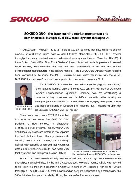
ASML NXT:1950i in-line with SOKUDO DUO<br />
lithography track inside IMEC 300mm clean room<br />
At the time many questioned why anyone would need such a high track run-rate when<br />
throughput is actually limited by the in-line exposure tool. However, recently ASML was reported<br />
to be extending their third-generation NXT:1950i immersion ArF scanners with up to 300wph<br />
throughput. The SOKUDO DUO track established an early market position by demonstrating the<br />
300wph in-line throughput capability utilizing the dual wafer flow track platform.
<strong>Sokudo</strong> also established an early start in E-beam maskless lithography by joining the<br />
CEA-LETI consortia program back in 2010 and now utilizes their on-site <strong>Sokudo</strong> RF3 coat track<br />
for Directed Self-Assembly (DSA) materials processing. CEA-LETI is now planning 300mm<br />
clean room layout to make space for new SOKUDO DUO track that can be in-line with next<br />
MAPPER E-beam exposure tool.<br />
“<strong>Sokudo</strong> is also integrating into SOKUDO DUO the best of Dainippon Screen’s single wafer<br />
cleaning technologies to address semiconductor manufacturer’s lithography process challenges,”<br />
indicated Charles Pieczulewski, Director of Strategic Marketing at <strong>Sokudo</strong> Co., Ltd., “Our<br />
post-develop accelerated wafer drying technology has begun to demonstrate clear semiconductor<br />
process yield advantages and reduced pattern collapse potential for critical lithography resist<br />
features in customer beta site qualifications.”<br />
SOKUDO DUO Track Post-Develop process Accelerated Purge (AP) dry technique<br />
Two years ago, November 2010, Dainippon Screen introduced into their SU-3200<br />
single-wafer cleaning system a proprietary “Air Protection Nozzle” (APN) technology that prevents<br />
the adhesion of contaminants and watermark-free wafer drying. <strong>Sokudo</strong> recognized the potential<br />
value of such a technique and adapted from their parent company this know-how into the<br />
SOKUDO DUO track system develop process module. <strong>Sokudo</strong> established the Accelerated<br />
Purge (AP) drying technique as a pattern collapse prevention method which does not use a<br />
surfactant rinse agent “demonstrating advantages of yield improvement, process time reduction<br />
and chemical cost reduction” per their technical abstract at the upcoming SPIE Advanced<br />
Lithography technical conference in San Jose, California.<br />
SOKUDO Co., Ltd. (Headquarters: Kyoto, Japan) is a subsidiary company of Dainippon<br />
Screen Mfg. Co., Ltd. established in 2006 for the development, manufacture, sales and service of<br />
advanced coat/develop track equipment for semiconductor production. Additional<br />
information on SOKUDO can be found at www.sokudo.com website.