DG9411 Low-Voltage Single SPDT Analog Switch - Darlas
DG9411 Low-Voltage Single SPDT Analog Switch - Darlas
DG9411 Low-Voltage Single SPDT Analog Switch - Darlas

You also want an ePaper? Increase the reach of your titles
YUMPU automatically turns print PDFs into web optimized ePapers that Google loves.
New Product<br />
<strong>DG9411</strong><br />
Vishay Siliconix<br />
<strong>Low</strong>-<strong>Voltage</strong> <strong>Single</strong> <strong>SPDT</strong> <strong>Analog</strong> <strong>Switch</strong><br />
FEATURES<br />
BENEFITS<br />
APPLICATIONS<br />
<strong>Low</strong> <strong>Voltage</strong> Operation (2.25 V to 5.5 V)<br />
<strong>Low</strong> On-Resistance - r DS(on ): 7 <br />
Fast <strong>Switch</strong>ing - t ON : 9 ns, t OFF : 5 ns<br />
<strong>Low</strong> Charge Injection - Q INJ : 5 pC<br />
<strong>Low</strong> Power Consumption<br />
TTL/CMOS Compatible<br />
6-Pin SC-70 Package<br />
Reduced Power Consumption<br />
Simple Logic Interface<br />
High Accuracy<br />
Reduce Board Space<br />
Cellular Phones<br />
Communication Systems<br />
Portable Test Equipment<br />
Battery Operated Systems<br />
Sample and Hold Circuits<br />
DESCRIPTION<br />
The <strong>DG9411</strong> is a single-pole/double-throw monolithic CMOS<br />
analog switch designed for high performance switching of<br />
analog signals. Combining low power, high speed (t ON : 9 ns,<br />
t OFF : 5 ns), low on-resistance (r DS(on) : 7 ) and small physical<br />
size (SC70), the <strong>DG9411</strong> is ideal for portable and battery<br />
powered applications requiring high performance and efficient<br />
use of board space.<br />
The <strong>DG9411</strong> is built on Vishay Siliconix’s low voltage JI2<br />
process. An epitaxial layer prevents latchup. Break-before<br />
-make is guaranteed for <strong>DG9411</strong>.<br />
Each switch conducts equally well in both directions when on,<br />
and blocks up to the power supply level when off.<br />
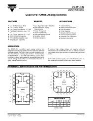
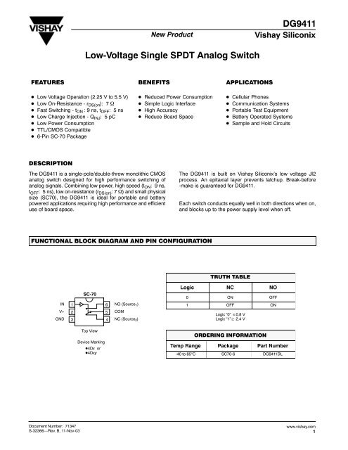
FUNCTIONAL BLOCK DIAGRAM AND PIN CONFIGURATION<br />
TRUTH TABLE<br />
SC-70<br />
IN<br />
V+<br />
GND<br />
1<br />
2<br />
3<br />
6<br />
5<br />
4<br />
NO (Source 1 )<br />
COM<br />
NC (Source 2 )<br />
Logic NC NO<br />
0 ON OFF<br />
1 OFF ON<br />
Logic “0” 0.8 V<br />
Logic “1” 2.4 V<br />
Top View<br />
Device Marking<br />
4Dx or<br />
4Dxy<br />
ORDERING INFORMATION<br />
Temp Range Package Part Number<br />
-40 to 85°C SC70-6 <strong>DG9411</strong>DL<br />
Document Number: 71347<br />
S-32366—Rev. B, 11-Nov-03<br />
www.vishay.com<br />
1
<strong>DG9411</strong><br />
Vishay Siliconix<br />
New Product<br />
ABSOLUTE MAXIMUM RATINGS<br />
Reference to GND<br />
V+ . . . . . . . . . . . . . . . . . . . . . . . . . . . . . . . . . . . . . . . . . . . . . . . . . . . . -0.3 to +6 V<br />
IN, COM, NC, NO a . . . . . . . . . . . . . . . . . . . . . . . . . . . . . . . . . . . . . . . -0.3 to (V+ + 0.3 V)<br />
Continuous Current (Any terminal) . . . . . . . . . . . . . . . . . . . . . . . . . . . 50 mA<br />
Peak Current . . . . . . . . . . . . . . . . . . . . . . . . . . . . . . . . . . . . . . . . . . . . . 200 mA<br />
(Pulsed at 1 ms, 10% duty cycle)<br />
Storage Temperature (D Suffix) . . . . . . . . . . . . . . . . . . . . . . . . . . . . -65 to 125°C<br />
Power Dissipation (Packages) b<br />
6-Pin SO70 c . . . . . . . . . . . . . . . . . . . . . . . . . . . . . . . . . . . . . . . . . . . . . . . 250 mW<br />
Notes:<br />
a. Signals on NC, NO, or COM or IN exceeding V+ will be clamped by<br />
internal diodes. Limit forward diode current to maximum current ratings.<br />
b. All leads welded or soldered to PC Board.<br />
c. Derate 6.5 mW/C above 25C<br />
SPECIFICATIONS (V+ = 2.5 V)<br />
Test Conditions<br />
Otherwise Unless Specified<br />
Limits<br />
−40 to 85C<br />
<strong>Analog</strong> <strong>Switch</strong><br />
Parameter Symbol V+ = 2.5 V, 10%, V IN = 0.4 or 2.0 V e Temp a Min b Typ c Max b Unit<br />
<strong>Analog</strong> Signal Range d V NO , V NC ,<br />
V COM<br />
Full 0 V+ V<br />
Drain-Source On-Resistance r DS(on) V+ = 2.25 V, V D = 1.0 V, I S = 10 mA<br />
r DS(on) Flatness d<br />
r DS(on)<br />
Flatness<br />
I S(off) <strong>Switch</strong> Off Leakage Current f V+ = 2.75 V<br />
V S = 0.5 V/1.5 V, V D = 1.5 V/0.5 V<br />
I D(off)<br />
Channel-On Leakage Current f I D(on) V+ = 2.75 V, V S = V D = 0.5 V/1.5 V<br />
Digital Control<br />
Room<br />
26<br />
Full d 29<br />
V+ = 2.5 V Room 10<br />
Room<br />
Full d<br />
Room<br />
Full d<br />
Room<br />
Full d<br />
−250<br />
−3.0<br />
−250<br />
−3.0<br />
−250<br />
−3.0<br />
35<br />
40<br />
250<br />
3.0<br />
250<br />
3.0<br />
250<br />
3.0<br />
<br />
pA<br />
nA<br />
pA<br />
nA<br />
pA<br />
nA<br />
Input High <strong>Voltage</strong> V INH Full 2<br />
Input <strong>Low</strong> <strong>Voltage</strong> V INL Full 0.4<br />
Input Capacitance d C in Full 3 pF<br />
Input Current I INL or I INH V IN = 0 or V+ Full −1 1 A<br />
Dynamic Characteristics<br />
Turn-Off Time t OFF Figures 1 and 2<br />
V D or V S = 15 1.5 V, R L = 300 , C L = 35 pF<br />
Turn-On Time t ON<br />
Room<br />
16 40<br />
Full d 45<br />
Room<br />
7 23<br />
Full d 28<br />
Break-Before-Make Time t d Room 1 12<br />
Charge Injection d Q INJ<br />
C L = 1 nF, V S = 0 V<br />
V GEN = 0 V, R GEN = 0 , Figure 3<br />
Off-Isolation d<br />
OIRR<br />
Crosstalk d X TALK R L = 50 , C L = 5 pF, f = 1 MHz<br />
V<br />
Room 5 10 pC<br />
Source-Off Capacitance d C S(off) Room 7<br />
Drain-to-Source Capacitance d C DS(off) Room 20<br />
Channel-On Capacitance d C D(on) V IN = 0 or V+, f = 1 MHz Room 20 pF<br />
Power Supply<br />
Power Supply Range V+ 2.25 2.75 V<br />
Power Supply Current d I+<br />
Power Consumption P C V IN = 0 or V+<br />
Room<br />
Room<br />
−73<br />
−70<br />
ns<br />
dB<br />
0.01 1.0 A<br />
0.3 W<br />
www.vishay.com<br />
2<br />
Document Number: 71347<br />
S-32366—Rev. B, 11-Nov-03
New Product<br />
<strong>DG9411</strong><br />
Vishay Siliconix<br />
SPECIFICATIONS (V+ = 3 V)<br />
Test Conditions<br />
Otherwise Unless Specified<br />
Limits<br />
−40 to 85C<br />
<strong>Analog</strong> <strong>Switch</strong><br />
Parameter Symbol V+ = 3 V, 10%, V IN = 0.4 or 2.0 V e Temp a Min b Typ c Max b Unit<br />
<strong>Analog</strong> Signal Range d V NO , V NC ,<br />
V COM<br />
Full 0 V+ V<br />
Drain-Source On-Resistance d r DS(on) V+ = 2.7 V, V D = 1.5 V, I S = 10 mA<br />
r DS(on) Flatness d<br />
r DS(on)<br />
Flatness<br />
I S(off) <strong>Switch</strong> Off Leakage Current f<br />
V+ = 3.33 V, V S = 1 V/3 V, V D = 3 V/1 V<br />
I D(off)<br />
Channel-On Leakage Current f I D(on) V+ = 3.3 V, V S = V D = 1 V/3 V<br />
Digital Control<br />
Room<br />
Full<br />
15<br />
19<br />
V S = 0 to V+, I S = 10 mA Room 7.5<br />
Room<br />
Full<br />
Room<br />
Full<br />
Room<br />
Full<br />
−500<br />
−4.0<br />
−500<br />
−4.0<br />
−500<br />
−4.0<br />
25<br />
30<br />
500<br />
4.0<br />
500<br />
4.0<br />
500<br />
4.0<br />
<br />
pA<br />
nA<br />
pA<br />
nA<br />
pA<br />
nA<br />
Input High <strong>Voltage</strong> V INH Full 2<br />
Input <strong>Low</strong> <strong>Voltage</strong> V INL Full 0.8<br />
Input Capacitance d C in Full 3 pF<br />
Input Current I INL or I INH V IN = 0 or V+ Full −1 1 A<br />
Dynamic Characteristics<br />
Turn-Off Time d t OFF Figure 1 and 2<br />
V D or V S = 20 2.0 V, R L = 300 , C L = 35 pF<br />
Turn-On Time d t ON<br />
Break-Before-Make Time d t d Room 1 7<br />
Charge Injection d Q INJ<br />
C L = 1 nF, V GEN = 0 V, V S = 0 V<br />
R GEN = 0 , Figure 3<br />
Off-Isolation d<br />
OIRR<br />
Crosstalk d X TALK R L = 50 , C L = 5 pF, f = 1 MHz<br />
Room<br />
Full<br />
Room<br />
Full<br />
12 15<br />
20<br />
6 8<br />
10<br />
V<br />
Room 5 10 pC<br />
Source-Off Capacitance d C S(off) Room 7<br />
Drain-to-Source Capacitance d C DS(off) Room 20<br />
Channel-On Capacitance d C D(on) V IN = 0 or V+, f = 1 MHz Room 20 pF<br />
Power Supply<br />
Power Supply Range V+ 2.7 3.3 V<br />
Power Supply Current I+<br />
Power Consumption P C V IN = 0 or V+<br />
Room<br />
Room<br />
−73<br />
−70<br />
ns<br />
dB<br />
0.01 1.0 A<br />
0.4 W<br />
Document Number: 71347<br />
S-32366—Rev. B, 11-Nov-03<br />
www.vishay.com<br />
3
<strong>DG9411</strong><br />
Vishay Siliconix<br />
New Product<br />
SPECIFICATIONS (V+ = 5 V)<br />
Test Conditions<br />
Otherwise Unless Specified<br />
Limits<br />
−40 to 85C<br />
<strong>Analog</strong> <strong>Switch</strong><br />
Parameter Symbol V+ = 5 V, 10%, V IN = 0.8 or 2.4 V e Temp a Min b Typ c Max b Unit<br />
<strong>Analog</strong> Signal Range d V NO , V NC ,<br />
V COM<br />
Full 0 V+ V<br />
Drain-Source On-Resistance r DS(on) V+ = 4.5 V, V D = 3 V, I S = 10 mA<br />
r DS(on) Flatness d<br />
<strong>Switch</strong> Off Leakage Current<br />
r DS(on)<br />
Flatness<br />
I S(off)<br />
I D(off)<br />
Room<br />
Full<br />
V+ = 2.5 V Room 2<br />
V+ = 5.5 V<br />
V S = 1 V/4.5 V, V D = 4.5 V/1 V<br />
Channel-On Leakage Current I D(on) V+ = 5.5 V, V S = V D = 1 V/4.5 V<br />
Digital Control<br />
Room<br />
Full<br />
Room<br />
Full<br />
Room<br />
Full<br />
−1.0<br />
−4.0<br />
−1.0<br />
−4.0<br />
−1.0<br />
−3.0<br />
7<br />
10<br />
12<br />
16<br />
1.0<br />
4.0<br />
1.0<br />
4.0<br />
1.0<br />
4.5<br />
<br />
nA<br />
Input High <strong>Voltage</strong> V INH Full 2.4<br />
Input <strong>Low</strong> <strong>Voltage</strong> V INL Full 0.8<br />
Input Capacitance C in Full 3 pF<br />
Input Current I INL or I INH V IN = 0 or V+ Full −1 1 A<br />
Dynamic Characteristics<br />
Turn-Off Time d t OFF Figure 1 and 2<br />
V D or V S = 3 V, R L = 300 , C L = 35 pF<br />
Turn-On Time d t ON<br />
Break-Before-Make Time d t d Room 1 4<br />
Charge Injection d Q INJ<br />
C L = 1 nF, V S = 0 V<br />
V GEN = 0 V, R GEN = 0 , Figure 3<br />
Off-Isolation d<br />
OIRR<br />
Crosstalk d X TALK R L = 50 , C L = 5 pF, f = 1 MHz<br />
Room<br />
Full<br />
Room<br />
Full<br />
9 11<br />
15<br />
5 7<br />
9<br />
V<br />
Room 5 10 pC<br />
Source-Off Capacitance d C S(off) Room 7<br />
Drain-to-Source Capacitance d C DS(off) Room 20<br />
Channel-On Capacitance d C D(on) V IN = 0 or V+, f = 1 MHz Room 20 pF<br />
Power Supply<br />
Power Supply Range V+ 4.5 5.5 V<br />
Power Supply Current I+<br />
Power Consumption P C V IN = 0 or V+<br />
Notes:<br />
a. Room = 25°C, Full = as determined by the operating suffix.<br />
b. The algebraic convention whereby the most negative value is a minimum and the most positive a maximum, is used in this data sheet.<br />
c. Typical values are for design aid only, not guaranteed nor subject to production testing.<br />
d. Guarantee by design, nor subjected to production test.<br />
e. V IN = input voltage to perform proper function.<br />
f. Guaranteed by 5-V leakage testing, not production tested.<br />
Room<br />
Room<br />
−73<br />
−70<br />
ns<br />
dB<br />
0.01 1.0 A<br />
0.6 W<br />
www.vishay.com<br />
4<br />
Document Number: 71347<br />
S-32366—Rev. B, 11-Nov-03
New Product<br />
<strong>DG9411</strong><br />
Vishay Siliconix<br />
TYPICAL CHARACTERISTICS (25C UNLESS NOTED)<br />
30<br />
r DS(on) vs. <strong>Analog</strong> and Power <strong>Voltage</strong><br />
30<br />
r DS(on) vs. <strong>Analog</strong> <strong>Voltage</strong> and Temperature<br />
r DS(on) − Drain-Source On-Resistance ( Ω )<br />
25<br />
20<br />
15<br />
10<br />
5<br />
V+ = 3 V<br />
V+ = 2.5 V<br />
V+ = 5 V<br />
r DS(on) − Drain-Source On-Resistance ( Ω )<br />
25<br />
20<br />
15<br />
10<br />
5<br />
V+ = 2.5 V<br />
V+ = 5 V<br />
−40C<br />
85C<br />
25C<br />
−40C<br />
25C<br />
85C<br />
0<br />
0 1 2 3 4 5<br />
0<br />
0 1 2 3 4 5<br />
V D − <strong>Analog</strong> <strong>Voltage</strong> (V)<br />
V D − <strong>Analog</strong> <strong>Voltage</strong> (V)<br />
100<br />
Supply Current vs. Temperature<br />
V+ = 5 V<br />
V IN = 0 V<br />
Supply Current vs. Input <strong>Switch</strong>ing Frequency<br />
10 mA<br />
1 mA<br />
I+ − Supply Current (nA)<br />
10<br />
1<br />
0.1<br />
I+ − Supply Current (nA)<br />
100 A<br />
10 A<br />
1 A<br />
100 pA<br />
10 pA<br />
0.01<br />
−60 −40 −20 0 20 40 60 80 100 120 140<br />
1 pA<br />
1<br />
10<br />
100<br />
1 K 10 K 100 K<br />
1 M 10 M<br />
Temperature (C)<br />
Input <strong>Switch</strong>ingFrequency (Hz)<br />
Leakage Current (pA)<br />
100 K<br />
10 K<br />
1 K<br />
100<br />
Leakage Current vs. Temperature<br />
V+ = 5 V<br />
V D , V S = 5 V<br />
I D(off)<br />
I D(on)<br />
Leakage Current (pA)<br />
100<br />
0<br />
−100<br />
−200<br />
−300<br />
−400<br />
Leakage vs. <strong>Analog</strong> <strong>Voltage</strong><br />
V+ = 5 V<br />
I D(off)<br />
I D(on)<br />
I S(off)<br />
10<br />
−500<br />
1<br />
−50 −25 0 25 50 75 100 125 150<br />
Temperature (C)<br />
−600<br />
0 1 2 3 4 5 6<br />
V D , V S − <strong>Analog</strong> <strong>Voltage</strong> (V)<br />
Document Number: 71347<br />
S-32366—Rev. B, 11-Nov-03<br />
www.vishay.com<br />
5
<strong>DG9411</strong><br />
Vishay Siliconix<br />
New Product<br />
TYPICAL CHARACTERISTICS (25C UNLESS NOTED)<br />
<strong>Switch</strong>ing Time vs. Temperature and Supply <strong>Voltage</strong><br />
25<br />
t ON<br />
100<br />
Crosstalk and Off Isolation vs. Frequency<br />
t ON , t OFF − <strong>Switch</strong>ing Time (nS)<br />
20<br />
15<br />
10<br />
5<br />
t OFF<br />
25C<br />
85C<br />
−40C<br />
25C<br />
85C<br />
−40C<br />
OIRR, X TALK (dB)<br />
80<br />
60<br />
40<br />
20<br />
V+ = 3 V<br />
R L = 50 <br />
Crosstalk<br />
Off Isolation<br />
0<br />
2.0 2.5 3.0 3.5 4.0 4.5 5.0 5.5<br />
V+ − Supply <strong>Voltage</strong> (V)<br />
0<br />
10 K 100 K 1 M 10 M 100 M<br />
Frequency (Hz)<br />
3.0<br />
Input <strong>Switch</strong>ing Threshold vs. Supply <strong>Voltage</strong><br />
0<br />
Insertion Loss vs. Frequency<br />
V T − Threshold <strong>Voltage</strong> (V)<br />
2.5<br />
2.0<br />
1.5<br />
1.0<br />
ËËËËËËË<br />
ËËËËËËË<br />
ËËËËËËË<br />
ËËËËËËË<br />
Insertion Loss (dB)<br />
−1<br />
−2<br />
−3<br />
−4<br />
V+ = 3 V<br />
R L = 50 <br />
0.5<br />
ËËËËËËË<br />
ËËËËËËË<br />
−5<br />
0.0<br />
0 1 2 3 4 5 6 7<br />
V+ − Supply <strong>Voltage</strong> (V)<br />
−6<br />
1 K<br />
10 K 100 K 1 M 10 M 100 M 1 G<br />
Frequency (Hz)<br />
Charge Injection (pC)<br />
6<br />
4<br />
2<br />
0<br />
−2<br />
−4<br />
Charge Injection vs. <strong>Analog</strong> <strong>Voltage</strong><br />
C L = 1 nF<br />
V+ = 2.5 V<br />
V+ = 3 V<br />
V+ = 5 V<br />
−6<br />
0 1 2 3 4 5 6<br />
V D − <strong>Analog</strong> <strong>Voltage</strong> (V)<br />
www.vishay.com<br />
6<br />
Document Number: 71347<br />
S-32366—Rev. B, 11-Nov-03
New Product<br />
<strong>DG9411</strong><br />
Vishay Siliconix<br />
TEST CIRCUITS<br />
<strong>Switch</strong><br />
Input<br />
Logic<br />
Input<br />
V+<br />
V+<br />
NO or NC<br />
IN<br />
GND<br />
COM<br />
<strong>Switch</strong> Output<br />
R L<br />
300 <br />
V OUT<br />
C L<br />
35 pF<br />
Logic<br />
Input<br />
<strong>Switch</strong><br />
Output<br />
+ 3 V<br />
0 V<br />
0 V<br />
t ON<br />
50%<br />
t r <br />
20 ns<br />
t f 20 ns<br />
0.9 x V OUT<br />
t OFF<br />
C L (includes fixture and stray capacitance)<br />
R<br />
V OUT<br />
V COM<br />
L<br />
R L R ON<br />
<br />
Logic “1” = <strong>Switch</strong> On<br />
Logic input waveforms inverted for switches that have<br />
the opposite logic sense.<br />
FIGURE 1. <strong>Switch</strong>ing Time<br />
V+<br />
V+<br />
Logic<br />
Input<br />
3 V<br />
t r
<strong>DG9411</strong><br />
Vishay Siliconix<br />
New Product<br />
TEST CIRCUITS<br />
V+<br />
10 nF<br />
V+<br />
COM<br />
IN<br />
0V, 2.4 V<br />
COM<br />
NC or NO<br />
R L<br />
GND<br />
V NCNO<br />
Off Isolation 20 log<br />
V COM<br />
Analyzer<br />
FIGURE 4. Off-Isolation<br />
V+<br />
10 nF<br />
V+<br />
COM<br />
Meter<br />
0 V, 2.4 V<br />
IN<br />
NC or NO<br />
HP4192A<br />
Impedance<br />
Analyzer<br />
or Equivalent<br />
GND<br />
f = 1 MHz<br />
FIGURE 5. Channel Off/On Capacitance<br />
www.vishay.com<br />
8<br />
Document Number: 71347<br />
S-32366—Rev. B, 11-Nov-03
Notice<br />
Legal Disclaimer Notice<br />
Vishay<br />
Specifications of the products displayed herein are subject to change without notice. Vishay Intertechnology, Inc.,<br />
or anyone on its behalf, assumes no responsibility or liability for any errors or inaccuracies.<br />
Information contained herein is intended to provide a product description only. No license, express or implied, by<br />
estoppel or otherwise, to any intellectual property rights is granted by this document. Except as provided in Vishay's<br />
terms and conditions of sale for such products, Vishay assumes no liability whatsoever, and disclaims any express<br />
or implied warranty, relating to sale and/or use of Vishay products including liability or warranties relating to fitness<br />
for a particular purpose, merchantability, or infringement of any patent, copyright, or other intellectual property right.<br />
The products shown herein are not designed for use in medical, life-saving, or life-sustaining applications.<br />
Customers using or selling these products for use in such applications do so at their own risk and agree to fully<br />
indemnify Vishay for any damages resulting from such improper use or sale.<br />
Document Number: 91000<br />
www.vishay.com<br />
Revision: 08-Apr-05 1