l1710s (l1710sm-al**r, au**r, ad**r, ag**r) - MobRepair.ru
l1710s (l1710sm-al**r, au**r, ad**r, ag**r) - MobRepair.ru
l1710s (l1710sm-al**r, au**r, ad**r, ag**r) - MobRepair.ru

Create successful ePaper yourself
Turn your PDF publications into a flip-book with our unique Google optimized e-Paper software.
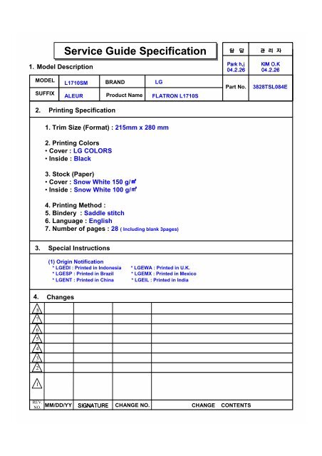
1.<br />
Model Description<br />
MODEL<br />
L1710SM BRAND<br />
SUFFIX<br />
2.<br />
3.<br />
4.<br />
8<br />
7<br />
6<br />
5<br />
4<br />
3<br />
2<br />
1<br />
REV.<br />
NO.<br />
Service Guide Specification<br />
ALEUR<br />
Printing Specification<br />
1. Trim Size (Format) : 215mm x 280 mm<br />
2. Printing Colors<br />
Cover : LG COLORS<br />
Inside : Black<br />
3. Stock (Paper)<br />
Cover : Snow White 150 g/����<br />
Inside : Snow White 100 g/����<br />
4. Printing Method :<br />
5. Bindery : Saddle stitch<br />
6. Language : English<br />
7. Number of pages : 28 ( Including blank 3pages)<br />
Special Inst<strong>ru</strong>ctions<br />
Changes<br />
���� ���� ���� ���� ����<br />
�������� �������� �������� ��������<br />
������� ������� ������� �������<br />
Part No.<br />
MM/DD/YY ���������<br />
���������<br />
���������<br />
��������� CHANGE NO. CHANGE CONTENTS<br />
LG<br />
Product Name FLATRON L1710S<br />
(1) Origin Notification<br />
* LGEDI : Printed in Indonesia * LGEWA : Printed in U.K.<br />
* LGESP : Printed in Brazil * LGEMX : Printed in Mexico<br />
* LGENT : Printed in China * LGEIL : Printed in India<br />
������� ������� ������� �������<br />
������� ������� ������� �������<br />
3828TSL084E
Cover<br />
Front cover<br />
Inside<br />
(Blank)<br />
English<br />
Contents<br />
2<br />
Pagination sheet<br />
English<br />
3<br />
English<br />
4<br />
English<br />
….<br />
English<br />
(blank)<br />
English<br />
…..<br />
Rear cover<br />
Inside<br />
(blank)<br />
English<br />
23<br />
Rear<br />
Cover<br />
����� ����������������<br />
����� �����<br />
�������������<br />
������������� �������������<br />
������������� �������<br />
English<br />
24
COLOR MONITOR<br />
SERVICE MANUAL<br />
CAUTION<br />
BEFORE SERVICING THE UNIT,<br />
READ THE SAFETY PRECAUTIONS IN THIS MANUAL.<br />
L1710B<br />
Website:http://biz.LGservice.com<br />
E-mail:http://www.LGEservice.com/techsup.html<br />
CHASSIS NO. : CL-61<br />
MODEL: L1710S (L1710SM-AL**R, AU**R, AD**R, AG**R)<br />
( ) **Same model for Service<br />
*Same looking with new chassis.<br />
Issue Date; 2004. 2
- 1 -
SPECIFICATIONS ................................................... 2<br />
PRECAUTIONS ....................................................... 3<br />
TIMING CHART ....................................................... 4<br />
OPERATING INSTRUCTIONS ................................ 5<br />
WIRING DIAGRAM ................................................. 6<br />
BLOCK DIAGRAM ................................................... 8<br />
1. LCD CHARACTERISTICS<br />
Type : TFT SXGA LCD<br />
Size : 17 inch<br />
Pixel Pitch : 0.264 (H) x 0.264 (V)<br />
Color Depth : 16.2M colors<br />
Electrical Interface : LVDS<br />
Surface Treatment : Hard-coating(3H), Anti-Glare<br />
Operating Mode : Normally White, Transmissive mode<br />
Backlight Unit : Top/Bottom edge side 4-CCFL<br />
(Cold Cathode Fluorescent Lamp)<br />
2. OPTICAL CHARACTERISTICS<br />
2-1. Viewing Angle by Contrast Ratio ≥ 10<br />
(LPL Module)<br />
Left : -60° min., -70°(Typ) Right : +60° min., +70°(Typ)<br />
Top :+45° min., +60°(Typ) Bottom : -45°min., -60°(Typ)<br />
(AU Module)<br />
Left : -60° min., -70°(Typ) Right : +60° min., +70°(Typ)<br />
Top :+60° min., +70°(Typ) Bottom : -60°min., -70°(Typ)<br />
(CMO Module)<br />
Left : -60° min., -70°(Typ) Right : +60° min., +70°(Typ)<br />
Top :+50° min., +60°(Typ) Bottom : -50°min., -60°(Typ)<br />
(Hydis Module)<br />
Left : -80°(Typ) Right : +80°(Typ)<br />
Top : +80°(Typ) Bottom : -60°(Typ)<br />
2-2. Luminance : 200(min), 250(Typ) -LPL Module<br />
200(min), 260(Typ) -AUO Module<br />
230(min), 280(Typ) -CMO Module<br />
250(min), 300(Typ) -Hydis Module<br />
2-3. Contrast Ratio : 300(min), 450(Typ)<br />
3. SIGNAL (Refer to the Timing Chart)<br />
3-1. Sync Signal<br />
• Type : Separate Sync,<br />
SOG (Sync On Green)<br />
Composite Sync<br />
3-2. Video Input Signal<br />
1) Type : R, G, B Analog<br />
2) Voltage Level : 0~0.71 V<br />
a) Color 0, 0 : 0 Vp-p<br />
b) Color 7, 0 : 0.467 Vp-p<br />
c) Color 15, 0 : 0.714 Vp-p<br />
3) Input Impedance : 75 Ω<br />
CONTENTS<br />
SPECIFICATIONS<br />
- 2 -<br />
DESCRIPTION OF BLOCK DIAGRAM.....................9<br />
ADJUSTMENT ....................................................... 11<br />
TROUBLESHOOTING GUIDE .............................. 13<br />
EXPLODED VIEW...................................................17<br />
REPLACEMENT PARTS LIST ...............................19<br />
SCHEMATIC DIAGRAM......................................... 21<br />
3-3. Operating Frequency<br />
Horizontal : 30 ~ 83kHz<br />
Vertical : 56 ~ 75Hz<br />
4. Max. Resolution<br />
Analog : 1280 x 1024 / 75Hz<br />
5. POWER SUPPLY<br />
5-1. Power : AC 100~240V, 50/60Hz , 1.0A<br />
5-2. Power Consumption<br />
MODE<br />
POWER ON (NORMAL)<br />
STAND-BY<br />
SUSPEND<br />
DPMS OFF<br />
6. ENVIRONMENT<br />
H/V SYNC<br />
ON/ON<br />
OFF/ON<br />
ON/OFF<br />
OFF/OFF<br />
6-1. Operating Temperature: 10°C~35°C (50°F~95°F)<br />
(Ambient)<br />
6-2. Relative Humidity : 10%~80%<br />
(Non-condensing)<br />
6-3. MTBF : 50,000 Hours(Min)<br />
7. DIMENSIONS (with TILT/SWIVEL)<br />
Width : 370 mm (14.57'')<br />
Depth : 222.5 mm (8.76'')<br />
Height : 421 mm (16.57'')<br />
8. WEIGHT (with TILT/SWIVEL)<br />
VIDEO POWER CONSUMPTION LED COLOR<br />
ACTIVE<br />
OFF<br />
OFF<br />
OFF<br />
less than 43 W<br />
less than 1 W<br />
less than 1 W<br />
less than 1 W<br />
Net. Weight : 6.0 kg (13.23 lbs)<br />
Gross Weight : 7.6 kg (16.76 lbs)<br />
GREEN<br />
AMBER<br />
AMBER<br />
AMBER
WARNING FOR THE SAFETY-RELATED COMPONENT.<br />
• There are some special components used in LCD<br />
monitor that are important for safety. These parts are<br />
marked on the schematic diagram and the<br />
replacement parts list. It is essential that these critical<br />
parts should be replaced with the manufacturer’s<br />
specified parts to prevent electric shock, fire or other<br />
hazard.<br />
• Do not modify original design without obtaining written<br />
permission from manufacturer or you will void the<br />
original parts and labor guarantee.<br />
TAKE CARE DURING HANDLING THE LCD MODULE<br />
WITH BACKLIGHT UNIT.<br />
• Must mount the module using mounting holes arranged<br />
in four corners.<br />
• Do not press on the panel, edge of the frame strongly<br />
or electric shock as this will result in damage to the<br />
screen.<br />
• Do not scratch or press on the panel with any sharp<br />
objects, such as pencil or pen as this may result in<br />
damage to the panel.<br />
• Protect the module from the ESD as it may damage the<br />
electronic circuit (C-MOS).<br />
• Make certain that treatment person’s body are<br />
grounded through wrist band.<br />
• Do not leave the module in high temperature and in<br />
areas of high humidity for a long time.<br />
• The module not be exposed to the direct sunlight.<br />
• Avoid contact with water as it may a short circuit within<br />
the module.<br />
• If the surface of panel become dirty, please wipe it off<br />
with a softmaterial. (Cleaning with a dirty or rough cloth<br />
may damage the panel.)<br />
CAUTION<br />
Please use only a plastic screwdriver to protect yourself<br />
from shock hazard during service operation.<br />
PRECAUTION<br />
- 3 -<br />
WARNING<br />
BE CAREFUL ELECTRIC SHOCK !<br />
• If you want to replace with the new backlight (CCFL) or<br />
inverter circuit, must disconnect the AC adapter<br />
because high voltage appears at inverter circuit about<br />
650Vrms.<br />
• Handle with care wires or connectors of the inverter<br />
circuit. If the wires are pressed cause short and may<br />
burn or take fire.
VIDEO<br />
SYNC<br />
C<br />
B<br />
TIMING CHART<br />
D<br />
F<br />
><br />
Mode<br />
1<br />
2<br />
3<br />
4<br />
5<br />
6<br />
7<br />
8<br />
9<br />
10<br />
11<br />
12<br />
13<br />
H/V<br />
Sort<br />
Sync<br />
Polarity<br />
Dot<br />
Clock<br />
Frequency<br />
Total Period<br />
(E)<br />
Video Active Time<br />
(A)<br />
H + 31.469 800 640 16 96 48<br />
25.175<br />
V – 70.8Hz 449 350 37 2 60<br />
H – 31.468 900 720 18 108 54<br />
28.321<br />
V + 70.09 449 400 12 2 35<br />
H<br />
V<br />
–<br />
–<br />
25.175<br />
31.469<br />
59.94<br />
840<br />
525<br />
640<br />
480<br />
16<br />
10<br />
96<br />
2<br />
48<br />
33<br />
H<br />
V<br />
–<br />
–<br />
31.5<br />
37.5<br />
75<br />
840<br />
500<br />
640<br />
480<br />
16<br />
1<br />
64<br />
3<br />
120<br />
16<br />
H<br />
V<br />
+<br />
+<br />
40.0<br />
37.879<br />
60.317<br />
1056<br />
628<br />
800<br />
600<br />
40<br />
1<br />
128<br />
4<br />
88<br />
23<br />
H<br />
V<br />
+<br />
+<br />
49.5<br />
46.875<br />
75.0<br />
1056<br />
625<br />
800<br />
600<br />
16<br />
1<br />
80<br />
3<br />
160<br />
21<br />
H<br />
V<br />
+/–<br />
+/–<br />
57.283<br />
49.725<br />
74.55<br />
1152<br />
667<br />
832<br />
624<br />
32<br />
1<br />
64<br />
3<br />
224<br />
39<br />
H<br />
V<br />
–<br />
–<br />
65.0<br />
48.363<br />
60.0<br />
1344<br />
806<br />
1024<br />
768<br />
24<br />
3<br />
136<br />
6<br />
160<br />
29<br />
H<br />
V<br />
–<br />
–<br />
78.75<br />
60.123<br />
75.029<br />
1312<br />
800<br />
1024<br />
768<br />
16<br />
1<br />
96<br />
3<br />
176<br />
28<br />
H<br />
V<br />
+/–<br />
+/–<br />
100.0<br />
68.681<br />
75.062<br />
1456<br />
915<br />
1152<br />
870<br />
32<br />
3<br />
128<br />
3<br />
144<br />
39<br />
H<br />
V<br />
+/–<br />
+/–<br />
92.978<br />
61.805<br />
65.96<br />
1504<br />
937<br />
1152<br />
900<br />
18<br />
2<br />
134<br />
4<br />
200<br />
31<br />
H<br />
V<br />
+<br />
+<br />
108.0<br />
63.981<br />
60.02<br />
1688<br />
1066<br />
1280<br />
1024<br />
48<br />
1<br />
112<br />
3<br />
248<br />
38<br />
H<br />
V<br />
+<br />
+<br />
135.0<br />
79.976<br />
75.035<br />
1688<br />
1066<br />
1280<br />
1024<br />
16<br />
1<br />
144<br />
3<br />
248<br />
38<br />
- 4 -<br />
A<br />
E<br />
Front Porch<br />
(C)<br />
Sync Duration<br />
(D)<br />
Back Porch<br />
(F)<br />
Resolution<br />
640x350<br />
70Hz<br />
720x400<br />
70Hz<br />
640x480<br />
60Hz<br />
640x480<br />
75Hz<br />
800x600<br />
60Hz<br />
800x600<br />
75Hz<br />
832x624<br />
75Hz<br />
1024x768<br />
60Hz<br />
1024x768<br />
75Hz<br />
1152x870<br />
75Hz<br />
1152x900<br />
65Hz<br />
1280x1024<br />
60Hz<br />
1280x1024<br />
75Hz
OPERATING INSTRUCTIONS<br />
FRONT VIEW REAR VIEW<br />
L1710B<br />
See Front Control Panel<br />
1. Power ON/OFF Button<br />
Use this button to turn the monitor on or off.<br />
2. Power Indicator<br />
This indicator lights up green when the monitor<br />
operates normally. If the display is in DPM(Energy<br />
Saving)mode, this indicator color change to amber.<br />
3. MENU Button<br />
Use these button to enter or exit the On Screen Display.<br />
4. Button<br />
Use these buttons to choose or adjust items in the On<br />
Screen Display.<br />
100<br />
100<br />
Bring up Contrast and Brightness<br />
adjustment.<br />
Front Control Panel<br />
6 3 4<br />
5<br />
- 5 -<br />
Power Connect<br />
1<br />
2<br />
D-Sub Signal<br />
Connect<br />
5. AUTO/SELECT Button<br />
Use this button to enter a selection in the On Screen Display.<br />
When adjusting your display settings,<br />
always press the AUTO/SELECT button<br />
before entering the On Screen<br />
Display(OSD). This will automatically<br />
adjust your display image to the ideal settings for the current<br />
screen resolution size (display mode).<br />
The best display mode is 1280x1024@60Hz.<br />
6. LIGHTVIEW Button<br />
Use this button to enter a selection in the on screen display.<br />
This feature lets you easily select the best desired image<br />
condition optimized to the environment (ambient<br />
illumination, image types etc.).<br />
• DAY: Bright ambient illuminaion<br />
• NIGHT: Dark ambient illuminaion<br />
• TEXT: For text images(Word processing etc.)<br />
• MOVIE: For animation images in videos or movies<br />
• PHOTO: For pictures or drawings<br />
• USER MODE: For use under user setup image<br />
conditions(Brigheness, contrast and color tint are<br />
selected by the user in OSD Screen Setup Menu.)
Connector Ass’y P/N:<br />
6631T20020Q<br />
J706<br />
J705<br />
M MST9151<br />
J702<br />
Main Board<br />
WIRING DIAGRAM<br />
(LG Philips/Hydis/CMO Module)<br />
Connector Ass’y P/N:<br />
6631T11012W<br />
LCD Module<br />
- 6 -<br />
Power Board<br />
Connector Ass’y P/N:<br />
6631T20024B<br />
J1<br />
Control Board
Connector Ass’y P/N:<br />
6631T20020Q<br />
J706<br />
J705<br />
M MST9151<br />
J702<br />
Main Board<br />
WIRING DIAGRAM<br />
(AU Module)<br />
Connector Ass’y P/N:<br />
6631T11012W<br />
LCD Module<br />
- 7 -<br />
Power Board<br />
Connector Ass’y P/N:<br />
6631T120024B<br />
Control Board
LCD Module<br />
5V<br />
LV DDS<br />
((LLoow VVoolltaaggee<br />
Diifffeerenntiiaall SSiiggnaling))<br />
3.3V<br />
5V<br />
R,G,B<br />
differential<br />
Diode<br />
KDS184<br />
3.3V<br />
Reg.<br />
BLOCK DIAGRAM<br />
3.3V 2.5V<br />
MTV312<br />
Micom<br />
MST9111B<br />
including<br />
(ADC/LVDS/SCALER )<br />
2.5V<br />
- 8 -<br />
3.3V<br />
5V<br />
12V<br />
R,G,B, H/V Sync<br />
LIPS<br />
AC Input<br />
D-SUB
DESCRIPTION OF BLOCK DIAGRAM<br />
1. Video Controller Part.<br />
This part amplifies the level of video signal for the digital conversion and converts from the analog video signal to the<br />
digital video signal using a pixel clock.<br />
The pixel clock for each mode is generated by the PLL.<br />
The range of the pixel clock is from 25MHz to 135MHz.<br />
This part consists of the Scaler, ADC, LVDS transmitter.<br />
The Scaler gets the video signal converted analog to digital, interpolates input to 1280 X 1024 resolution signal and<br />
outputs 8-bit R, G, B signal to transmitter.<br />
2. Power Part.<br />
This part consists of the one 3.3V regulator, and two 2.5V drop diodes to convert power which is provided 12V, 5V in<br />
Power board.<br />
5V is provided for LCD panel and Micom.<br />
Also, 5V is converted 3.3V by regulator and 3.3V is converted 2.5V by drop diode.<br />
Converted power is provided for IC in the main board.<br />
3. MICOM Part.<br />
This part consists of EEPROM IC which stores control data, Reset IC and the Micom.<br />
The Micom distinguishes polarity and frequency of the H/V sync are supplied from signal cable.<br />
The controlled data of each modes is stored in EEPROM.<br />
- 9 -
50 ~ 60Hz<br />
LINE<br />
100 ~ 240V<br />
EMI<br />
COMPONENTS<br />
LIPS Board Block Diagram<br />
INPUT RECTIFIER<br />
AND FILTER<br />
PWM<br />
CONTROL<br />
CIRCUIT<br />
HVDC<br />
- 10 -<br />
ENERGY<br />
TRANSFER<br />
PHOTO-<br />
COUPLER<br />
ISOLATION<br />
100KHz<br />
OUTPUT RECTIFIER<br />
AND FILTER<br />
SIGNAL<br />
COLLECTI<br />
ON<br />
PRIMARY SECONDARY<br />
Operation description_LIPS<br />
1. EMI components.<br />
This part contains of EMI components to comply with global marketing EMI standards like FCC, VCCI CISPR, the<br />
circuit included a line-filter, across line capacitor and of course the primary protection fuse.<br />
2. Input rectifier and filter.<br />
This part function is for transfer the input AC voltage to a DC voltage through a bridge rectifier and a bulk capacitor.<br />
3. Energy Transfer.<br />
This part function is transfer the primary energy to secondary through a power transformer.<br />
4. Output rectifier and filter.<br />
This part function is to make a pulse width modulation control and to provide the driver signal to power switch, to<br />
adjust the duty cycle during different AC input and output loading condition to achive the dc output stablize, and also<br />
the over power protection is also monitor by this part.<br />
5. Photo-Coupler isolation.<br />
This part function is to feed back the dc output changing status through a photo transistor to primary controller to<br />
achieve the stabilized dc output voltage.<br />
6. Signal collection.<br />
This part function is to collect the any change from the dc output and feed back to the primary through photo<br />
transistor.<br />
12V<br />
5V<br />
GND
Windows EDID V1.0 User Manual<br />
Operating System: MS Windows 98, 2000, XP<br />
Port Setup: Windows 98 => Don’t need setup<br />
Windows 2000, XP => Need to Port Setup.<br />
This program is available to LCD Monitor only.<br />
1. Port Setup<br />
a) Copy “UserPort.sys” file to<br />
“c:\WINNT\system32\drivers” folder<br />
b) Run Userport.exe<br />
c) Remove all default number<br />
d) Add 300-3FF<br />
e) Click Start button.<br />
f) Click Exit button.<br />
ADJUSTMENT<br />
- 11 -<br />
2. EDID Read & Write<br />
1) Run WinEDID.exe<br />
2) Edit Week of Manufacture, Year of Manufacture,<br />
Serial Number<br />
a) Input User Info Data<br />
b) Click “Update” button<br />
c) Click “ Write” button
Video Signal<br />
Generator<br />
Control Line<br />
C<br />
A<br />
Not used<br />
PARALLEL<br />
RS232C<br />
VGS MONITOR<br />
B<br />
V-SYNC ST POWER<br />
F<br />
IBM<br />
Compatible PC<br />
E<br />
220<br />
Power inlet (required)<br />
Power Select Switch<br />
(110V/220V)<br />
Power LED<br />
ST Switch<br />
V-Sync On/Off Switch<br />
(Switch must be ON.)<br />
SERVICE OSD<br />
1) Turn off the power switch at the front side of the display.<br />
2) Wait for about 3 seconds and press MENU, POWER switch with 1 second interval.<br />
3) The SVC OSD menu contains additional menus that the User OSD menu as described below.<br />
a) MODULE : To select applied module.<br />
b) NVRAM INIT : EEPROM initialize(24C08)<br />
c) ADC OFFSET : The lowest value of input leves sets to digitally 0(zero).<br />
d) ADC GAIN : The highest value of input levels sets to digitally 255.<br />
e) ADC CAL : W/B balance sets the gain and offset value.<br />
f) ELAPSED CLEAR : To initialize using time.<br />
PARALLEL PORT<br />
- 12 -<br />
5V<br />
F<br />
15<br />
10<br />
5<br />
OFF ON<br />
Figure 1. Cable Connection<br />
A<br />
B<br />
11<br />
6<br />
1<br />
5<br />
9<br />
ON<br />
OFF<br />
E<br />
6<br />
1<br />
13<br />
25<br />
5V<br />
74LS06<br />
4.7K<br />
C<br />
5V<br />
4.7K<br />
4.7K<br />
74LS06<br />
1<br />
14
NO POWER<br />
(POWER INDICATOR OFF)<br />
CHECK J705<br />
VOLTAGE<br />
PIN5, PIN6 (5V)?<br />
YES<br />
CHECK<br />
U501 PIN 8 Voltage<br />
(5V) ?<br />
YES<br />
CHECK KEY CONTROL<br />
CONNECTOR ROUTINE<br />
IS U201<br />
PIN114 (3.3V)<br />
VOLTAGE ?<br />
YES<br />
CHECK U201 PIN 122<br />
PULSE<br />
YES<br />
CHECK U201<br />
TROUBLESHOOTING GUIDE<br />
1. NO POWER<br />
NO<br />
NO<br />
NO<br />
NO<br />
- 13 -<br />
CHECK POWER<br />
BOARD, AND FIND<br />
OUT A SHORT POINT<br />
AS OPENING<br />
EACH POWER LINE<br />
CHECK 5VS LINE<br />
(OPEN CHECK)<br />
CHECK 3.3V LINE<br />
CHECK X-TAL<br />
NO PROBLEM
NO RASTER<br />
(OSD IS NOT DISPLAYED)<br />
J705<br />
PIN5, PIN6<br />
5V?<br />
J705 PIN9<br />
5V?<br />
J705 PIN10<br />
5V?<br />
2. NO RASTER (OSD IS NOT DISPLAYED) – LIPS<br />
YES<br />
YES<br />
YES<br />
CHECK<br />
PULSE AS<br />
CONTACTING SCOPE<br />
PROBE TO CAUTION LABEL.<br />
(CONTACT PROBE TO<br />
CAUTION LABEL.<br />
CAN YOU SEE PULSE<br />
AT YOUR<br />
SCOPE?<br />
YES<br />
REPLACE CCFL LAMP<br />
IN THE LCD MODULE<br />
NO<br />
NO<br />
NO<br />
NO<br />
- 14 -<br />
CHECK LIPS<br />
CHECK MICOM INV<br />
ON/OFF PORT.<br />
1. CONFIRM BRIGHTNESS<br />
OSD CONTRL STATE.<br />
2. CHECK MICOM DIM-ADJ<br />
PORT<br />
LIPS
3. NO RASTER (OSD IS NOT DISPLAYED) – MST9111B<br />
NO RASTER<br />
(OSD IS NOT DISPLAYED)<br />
U201<br />
POWER PIN 8,114<br />
3.3V?<br />
YES<br />
U201<br />
PIN122, 123<br />
OSCILLATE AS<br />
12MHZ?<br />
YES<br />
U501<br />
PIN43 IS 64KHz H-SYNC?<br />
PIN44 IS 60Hz V-SYNC?<br />
IS PULSE APPEARED<br />
AT SIGNAL PINS?<br />
AT MODE 12?<br />
YES<br />
TROUBLE IN CABLE<br />
OR LCD MODULE<br />
NO<br />
NO<br />
NO<br />
- 15 -<br />
CHECK U801<br />
1. CHECK PIN122, 123<br />
SOLDERING CONDITION<br />
2. CHECK X501<br />
3. TROUBLE IN U201<br />
CHECK CONNECTION LINE<br />
FROM D-SUB TO U501
TROUBLE IN DPM<br />
CHECK<br />
R773, R775<br />
(SYNC) ?<br />
YES<br />
CHECK<br />
U501 PIN 43.44<br />
SYNC PULSE ?<br />
YES<br />
TROUBLE IN U501<br />
4. TROUBLE IN DPM<br />
NO<br />
NO<br />
- 16 -<br />
CHECK PC<br />
PC IS NOT GOING<br />
INTO DPM OFF MODE<br />
CHECK H/V SYNC<br />
LINE
EXPLODED VIEW<br />
b<br />
a<br />
3<br />
6<br />
11<br />
7<br />
M MST9151<br />
- 17 -<br />
8<br />
5<br />
c<br />
2-1<br />
4<br />
9<br />
2<br />
10<br />
1
Ref. No.<br />
1<br />
2<br />
2-1<br />
3<br />
4<br />
5<br />
6<br />
7<br />
8<br />
9<br />
10<br />
11<br />
a<br />
b<br />
c<br />
Part No.<br />
3091TKL053L<br />
6304FLP086A<br />
6304FBH007A<br />
6304FCI005B<br />
6304FAU012A<br />
3809TKL035B<br />
3043TKK091E<br />
4814TKK231A<br />
4951TKS102U<br />
4951TKS102H<br />
4951TKS102B<br />
6871TPT271B<br />
6871TPT271D<br />
3313TL7027A<br />
3313TL7033A<br />
6631T11012W<br />
6871TST374A<br />
6850TD9004J<br />
or 6850TD9004D<br />
1SZZTMF008A<br />
332-113S<br />
332-105G<br />
EXPLODED VIEW PARTS LIST<br />
- 18 -<br />
Description<br />
CABINET ASSEMBLY, L1710SL BRAND 3090TKL053A HF350<br />
LCD(LIQUID CRYSTAL DISPLAY), LM170E01-A5K6 LG PHILPS TFT COLOR LVDS SXGA OKI GATE D-IC<br />
LCD(LIQUID CRYSTAL DISPLAY), HT17E13-100 BOE-HYDIS TFT COLOR LVDS SXGA<br />
LCD(LIQUID CRYSTAL DISPLAY), M170E_L05 CHIMEI TFT COLOR 300NITS 16MS TCO-03 TN SXGA<br />
LCD(LIQUID CRYSTAL DISPLAY), M170EN05V5 AU TFT COLOR SXGA 250NIT GEN5<br />
BACK COVER ASSEMBLY, LB700G 3808TKL039A HF350U<br />
TILT SWIVEL ASSEMBLY, LM805L -HIPS NO USB<br />
SHIELD, INVERTER LAMP WIRE,LB700K<br />
METAL ASSEMBLY, FRAME LPL,HD,1710SL<br />
METAL ASSEMBLY, FRAME L1710SL_CMO<br />
METAL ASSEMBLY, FRAME L1710SL_AU<br />
PWB(PCB) ASSEMBLY,POWER, L1710SM POWER TOTAL LIEN CHANG M-CHASSIS THE INTERGRATED LIPS FOR LPL,CMO,HD<br />
PWB(PCB) ASSEMBLY, POWER, "17" AUO M-CHASSIS POWER TOAL LIEN CHANG "INTEGRATED LIPS" -AU only<br />
MAIN TOTAL ASSEMBLY L1710SM BRAND CL-61<br />
MAIN TOTAL ASSEMBLY L1710SM BRAND CL-61 -AU only<br />
CONNECTOR ASSEMBLY, 30P H-H 200MM UL20276 LG708G<br />
PWB(PCB) ASSEMBLY, SUB, L1710BL CONTROL TOTAL BRAND CONTROL<br />
CABLE, D-SUB, UL20276-9C(5.8MM) DT 1500MM, CORE POS400MM GRAY(85964) L1720BM DM<br />
CABLE, D-SUB, UL20276-9C(5.8MM) DT 1500MM GRAY(85964) LB500L DM<br />
SCREW,DRAWING, D3.0 L6.0 MSWR/FZMY<br />
SCREW,DRAWING, D3.0 L12.0 MSWR/BK<br />
SCREW,DRAWING, PVS+4*10(MSWR/BK)
DATE: 2004. 2. 6.<br />
*S *AL LOC. NO. PART NO. DESCRIPTION / SPECIFICATION<br />
MAIN BOARD<br />
CAPACITORS<br />
C204 0CK104CK56A 0.1UF 1608 50V 10% R/TP X7R<br />
C205 0CK104CK56A 0.1UF 1608 50V 10% R/TP X7R<br />
C206 0CK104CK56A 0.1UF 1608 50V 10% R/TP X7R<br />
C207 0CK104CK56A 0.1UF 1608 50V 10% R/TP X7R<br />
C208 0CK104CK56A 0.1UF 1608 50V 10% R/TP X7R<br />
C209 0CK104CK56A 0.1UF 1608 50V 10% R/TP X7R<br />
C210 0CK104CK56A 0.1UF 1608 50V 10% R/TP X7R<br />
C211 0CK104CK56A 0.1UF 1608 50V 10% R/TP X7R<br />
C214 0CK104CK56A 0.1UF 1608 50V 10% R/TP X7R<br />
C215 0CK104CK56A 0.1UF 1608 50V 10% R/TP X7R<br />
C216 0CK104CK56A 0.1UF 1608 50V 10% R/TP X7R<br />
C217 0CK104CK56A 0.1UF 1608 50V 10% R/TP X7R<br />
C218 0CK104CK56A 0.1UF 1608 50V 10% R/TP X7R<br />
C219 0CK104CK56A 0.1UF 1608 50V 10% R/TP X7R<br />
C220 0CK104CK56A 0.1UF 1608 50V 10% R/TP X7R<br />
C221 0CK104CK56A 0.1UF 1608 50V 10% R/TP X7R<br />
C222 0CK104CK56A 0.1UF 1608 50V 10% R/TP X7R<br />
C223 0CK104CK56A 0.1UF 1608 50V 10% R/TP X7R<br />
C225 0CK104CK56A 0.1UF 1608 50V 10% R/TP X7R<br />
C226 0CK104CK56A 0.1UF 1608 50V 10% R/TP X7R<br />
C227 0CK104CK56A 0.1UF 1608 50V 10% R/TP X7R<br />
C230 0CK104CK56A 0.1UF 1608 50V 10% R/TP X7R<br />
C231 0CK104CK56A 0.1UF 1608 50V 10% R/TP X7R<br />
C232 0CK104CK56A 0.1UF 1608 50V 10% R/TP X7R<br />
C233 0CK104CK56A 0.1UF 1608 50V 10% R/TP X7R<br />
C240 0CK104CK56A 0.1UF 1608 50V 10% R/TP X7R<br />
C251 0CK104CK56A 0.1UF 1608 50V 10% R/TP X7R<br />
C501 0CC101CK41A 100PF 1608 50V 5% R/TP NP0<br />
C502 0CC101CK41A 100PF 1608 50V 5% R/TP NP0<br />
C503 0CK104CK56A 0.1UF 1608 50V 10% R/TP X7R<br />
C504 0CH8106F611 10UF 16V M 85STD(CYL) R/TP<br />
C506 0CC030CK01A 3PF 1608 50V 0.25 PF R/TP NP<br />
C507 0CC180CK41A 18PF 1608 50V 5% R/TP NP0<br />
C508 0CK104CK56A 0.1UF 1608 50V 10% R/TP X7R<br />
C701 0CK105CD56A 1UF 1608 10V 10% R/TP X7R<br />
C703 0CK104CK56A 0.1UF 1608 50V 10% R/TP X7R<br />
C708 0CK103CK51A 0.01UF 1608 50V 10% R/TP B(Y<br />
C709 0CK103CK51A 0.01UF 1608 50V 10% R/TP B(Y<br />
C710 0CK103CK51A 0.01UF 1608 50V 10% R/TP B(Y<br />
C711 0CK103CK51A 0.01UF 1608 50V 10% R/TP B(Y<br />
C717 0CC101CK41A 100PF 1608 50V 5% R/TP NP0<br />
C718 0CC101CK41A 100PF 1608 50V 5% R/TP NP0<br />
C719 0CC680CK41A 68PF 1608 50V 5% R/TP NP0<br />
C720 0CC101CK41A 100PF 1608 50V 5% R/TP NP0<br />
C721 0CC680CK41A 68PF 1608 50V 5% R/TP NP0<br />
C727 0CK105CD56A 1UF 1608 10V 10% R/TP X7R<br />
C732 0CK103CK51A 0.01UF 1608 50V 10% R/TP B(Y<br />
C733 0CK104CK56A 0.1UF 1608 50V 10% R/TP X7R<br />
C734 0CK104CK56A 0.1UF 1608 50V 10% R/TP X7R<br />
C735 0CK104CK56A 0.1UF 1608 50V 10% R/TP X7R<br />
C760 0CE107EF610 "100UF KMG,RD 16V 20% FL BULK"<br />
C801 0CK103CK51A 0.01UF 1608 50V 10% R/TP B(Y<br />
REPLACEMENT PARTS LIST<br />
CAUTION: BEFORE REPLACING ANY OF THESE COMPONENTS,<br />
READ CAREFULLY THE SAFETY PRECAUTIONS IN THIS MANUAL.<br />
* NOTE : S SAFETY Mark<br />
AL ALTERNATIVE PARTS<br />
- 19 -<br />
DATE: 2004. 2. 6.<br />
*S *AL LOC. NO. PART NO. DESCRIPTION / SPECIFICATION<br />
C803 0CE107EF610 "100UF KMG,RD 16V 20% FL BULK"<br />
C804 0CK104CK56A 0.1UF 1608 50V 10% R/TP X7R<br />
C805 0CK104CK56A 0.1UF 1608 50V 10% R/TP X7R<br />
C805 0CK105CD56A 1UF 1608 10V 10% R/TP X7R-OnlyAuo Module<br />
C806 0CK103CK51A 0.01UF 1608 50V 10% R/TP B(Y<br />
C807 0CE107EF610 "100UF KMG,RD 16V 20% FL BULK"<br />
C808 0CK104CK56A 0.1UF 1608 50V 10% R/TP X7R<br />
C809 0CK103CK51A 0.01UF 1608 50V 10% R/TP B(Y<br />
C810 0CK104CK56A 0.1UF 1608 50V 10% R/TP X7R<br />
C812 0CE107EF610 "100UF KMG,RD 16V 20% FL BULK"<br />
C814 0CE107EF610 "100UF KMG,RD 16V 20% FL BULK"<br />
C815 0CK104CK56A 0.1UF 1608 50V 10% R/TP X7R<br />
C816 0CK103CK51A 0.01UF 1608 50V 10% R/TP<br />
C817 0CK104CK56A 0.1UF 1608 50V 10% R/TP X7R-OnlyAuo Module<br />
C818 0CC102CK41A 1000PF 1608 50V 5% R/TP -OnlyAuo Module<br />
DIODEs<br />
ICs<br />
D701 0DS226009AA KDS226 TP KEC SOT-23 80V 30<br />
D702 0DS226009AA KDS226 TP KEC SOT-23 80V 30<br />
D706 0DS226009AA KDS226 TP KEC SOT-23 80V 30<br />
D804 0DD184009AA KDS184 TP KEC - 85V - - - 30<br />
D805 0DD184009AA KDS184 TP KEC - 85V - - - 30<br />
ZD701 0DZ560009GB BZT52C5V6S DIODES R/TP SOD32<br />
ZD702 0DZ560009GB BZT52C5V6S DIODES R/TP SOD32<br />
ZD703 0DZ560009GB BZT52C5V6S DIODES R/TP SOD32<br />
ZD704 0DZ560009GB BZT52C5V6S DIODES R/TP SOD32<br />
ZD705 0DZ560009GB BZT52C5V6S DIODES R/TP SOD32<br />
ZD711 0DZ560009GB BZT52C5V6S DIODES R/TP SOD32<br />
U201 0IPRPM3008B "MST9111B(ANALOG) MSTAR 128P,"<br />
U501 0IZZTSZ328A M-CHASSIS MYSON 44P PLCC ST<br />
U502 0ISG240860B M24C08W6 SGS-THOMSON 8SOP R/<br />
U801 0IPMGKE011A KIA78D33F KEC DPAK R/TP 3.3V<br />
U802 0TFVI80023A VISHAY SI3865DV R/TP TSOP-Only Auo Module<br />
TRANSISTOR<br />
Q502 0IKE704200H KIA7042AP TO-92 TP 4.2 VOLT<br />
Q503 0TR390409AE FAIRCHILD KST3904(LGEMTF) TP<br />
Q504 0TR390409AE FAIRCHILD KST3904(LGEMTF) TP<br />
Q505 0TR390409AE FAIRCHILD KST3904(LGEMTF) TP<br />
Q703 0TR390609FA KST3906-MTF TP SAMSUNG SOT2<br />
Q704 0TR390609FA KST3906-MTF TP SAMSUNG SOT2<br />
Q706 0TR390409AE FAIRCHILD KST3904(LGEMTF) TP<br />
Q707 0TR390409AE FAIRCHILD KST3904(LGEMTF) TP<br />
Q801 0TR127309AA KTA1273-Y(KTA966A) TP KEC TO<br />
Q802 0TR390409AE FAIRCHILD KST3904(LGEMTF) TP<br />
RESISTORs<br />
R201 0RJ0682D677 68 OHM 1/10 W 5% 1608 R/TP
DATE: 2004. 2. 6.<br />
*S *AL LOC. NO. PART NO. DESCRIPTION / SPECIFICATION<br />
R202 0RJ0682D677 68 OHM 1/10 W 5% 1608 R/TP<br />
R203 0RJ0682D677 68 OHM 1/10 W 5% 1608 R/TP<br />
R207 0RJ3900D677 390 OHM 1/10 W 5% 1608 R/TP<br />
R208 0RJ0682D677 68 OHM 1/10 W 5% 1608 R/TP<br />
R209 0RJ0682D677 68 OHM 1/10 W 5% 1608 R/TP<br />
R210 0RJ0682D677 68 OHM 1/10 W 5% 1608 R/TP<br />
R213 0RJ0000D677 0 OHM 1/10 W 5% 1608 R/TP<br />
R214 0RJ0000D677 0 OHM 1/10 W 5% 1608 R/TP<br />
R220 0RJ4701D677 4.7K OHM 1/10 W 5% 1608 R/TP<br />
R240 0RJ1001D677 1K OHM 1/10 W 5% 1608 R/TP<br />
R506 0RJ4701D677 4.7K OHM 1/10 W 5% 1608 R/TP<br />
R508 0RJ4701D677 4.7K OHM 1/10 W 5% 1608 R/TP<br />
R512 0RJ0332D677 33 OHM 1/10 W 5% 1608 R/TP<br />
R513 0RJ0332D677 33 OHM 1/10 W 5% 1608 R/TP<br />
R514 0RJ4701D677 4.7K OHM 1/10 W 5% 1608 R/TP<br />
R515 0RJ4701D677 4.7K OHM 1/10 W 5% 1608 R/TP<br />
R516 0RJ4701D677 4.7K OHM 1/10 W 5% 1608 R/TP<br />
R518 0RJ4701D677 4.7K OHM 1/10 W 5% 1608 R/TP<br />
R519 0RJ1000D677 100 OHM 1/10 W 5% 1608 R/TP<br />
R520 0RJ4701D677 4.7K OHM 1/10 W 5% 1608 R/TP<br />
R521 0RJ4701D677 4.7K OHM 1/10 W 5% 1608 R/TP<br />
R522 0RJ4701D677 4.7K OHM 1/10 W 5% 1608 R/TP<br />
R523 0RJ4701D677 4.7K OHM 1/10 W 5% 1608 R/TP<br />
R524 0RJ1000D677 100 OHM 1/10 W 5% 1608 R/TP<br />
R525 0RJ1000D677 100 OHM 1/10 W 5% 1608 R/TP<br />
R526 0RJ1000D677 100 OHM 1/10 W 5% 1608 R/TP<br />
R527 0RJ1000D677 100 OHM 1/10 W 5% 1608 R/TP<br />
R528 0RJ1000D677 100 OHM 1/10 W 5% 1608 R/TP<br />
R529 0RJ1000D677 100 OHM 1/10 W 5% 1608 R/TP<br />
R531 0RJ1000D677 100 OHM 1/10 W 5% 1608 R/TP<br />
R532 0RJ1000D677 100 OHM 1/10 W 5% 1608 R/TP<br />
R534 0RJ0000D677 0 OHM 1/10 W 5% 1608 R/TP<br />
R535 0RJ3301D677 3.3K OHM 1/10 W 5% 1608 R/TP<br />
R537 0RJ3301D677 3.3K OHM 1/10 W 5% 1608 R/TP<br />
R541 0RJ1000D677 100 OHM 1/10 W 5% 1608 R/TP<br />
R542 0RJ1000D677 100 OHM 1/10 W 5% 1608 R/TP<br />
R543 0RJ4701D677 4.7K OHM 1/10 W 5% 1608 R/TP<br />
R544 0RJ4701D677 4.7K OHM 1/10 W 5% 1608 R/TP<br />
R545 0RJ4700D677 470 OHM 1/10 W 5% 1608 R/TP<br />
R546 0RJ4701D677 4.7K OHM 1/10 W 5% 1608 R/TP<br />
R547 0RJ4700D677 470 OHM 1/10 W 5% 1608 R/TP<br />
R548 0RJ0332D677 33 OHM 1/10 W 5% 1608 R/TP<br />
R549 0RJ0332D677 33 OHM 1/10 W 5% 1608 R/TP<br />
R555 0RJ1000D677 100 OHM 1/10 W 5% 1608 R/TP<br />
R556 0RJ4700D677 470 OHM 1/10 W 5% 1608 R/TP<br />
R557 0RJ1000D677 100 OHM 1/10 W 5% 1608 R/TP<br />
R560 0RJ1001D677 1K OHM 1/10 W 5% 1608 R/TP-LPL Module<br />
R560 0RJ4702D677 47000 OHM 1/10 W 5% 1608 R/T-Auo Module<br />
R561 0RJ4701D677 4.7K OHM 1/10 W 5% 1608 R/TP<br />
R563 0RJ1000D677 100 OHM 1/10 W 5% 1608 R/TP<br />
R564 0RJ1000D677 100 OHM 1/10 W 5% 1608 R/TP<br />
R565 0RJ1000D677 100 OHM 1/10 W 5% 1608 R/TP<br />
R566 0RJ1002D677 10K OHM 1/10 W 5% 1608 R/TP<br />
R701 0RJ0752D677 75 OHM 1/10 W 5% 1608 R/TP<br />
R703 0RJ0752D677 75 OHM 1/10 W 5% 1608 R/TP<br />
R706 0RJ0752D677 75 OHM 1/10 W 5% 1608 R/TP<br />
R708 0RJ4700D677 470 OHM 1/10 W 5% 1608 R/TP<br />
R709 0RJ1001D677 1K OHM 1/10 W 5% 1608 R/TP<br />
R716 0RJ4701D677 4.7K OHM 1/10 W 5% 1608 R/TP<br />
R717 0RJ4701D677 4.7K OHM 1/10 W 5% 1608 R/TP<br />
R720 0RJ0000D677 0 OHM 1/10 W 5% 1608 R/TP<br />
R722 0RJ1000D677 100 OHM 1/10 W 5% 1608 R/TP<br />
- 20 -<br />
DATE: 2004. 2. 6.<br />
*S *AL LOC. NO. PART NO. DESCRIPTION / SPECIFICATION<br />
R723 0RJ0332D677 33 OHM 1/10 W 5% 1608 R/TP<br />
R724 0RJ0332D677 33 OHM 1/10 W 5% 1608 R/TP<br />
R726 0RJ1002D677 10K OHM 1/10 W 5% 1608 R/TP<br />
R727 0RJ1002D677 10K OHM 1/10 W 5% 1608 R/TP<br />
R737 0RJ0000D677 0 OHM 1/10 W 5% 1608 R/TP<br />
R744 0RJ4701D677 4.7K OHM 1/10 W 5% 1608 R/TP<br />
R745 0RJ4701D677 4.7K OHM 1/10 W 5% 1608 R/TP<br />
R747 0RJ4701D677 4.7K OHM 1/10 W 5% 1608 R/TP<br />
R748 0RJ4701D677 4.7K OHM 1/10 W 5% 1608 R/TP<br />
R769 0RJ0000D677 0 OHM 1/10 W 5% 1608 R/TP<br />
R772 0RJ1001D677 1K OHM 1/10 W 5% 1608 R/TP<br />
R773 0RJ4701D677 4.7K OHM 1/10 W 5% 1608 R/TP<br />
R774 0RJ1001D677 1K OHM 1/10 W 5% 1608 R/TP<br />
R775 0RJ4701D677 4.7K OHM 1/10 W 5% 1608 R/TP<br />
R779 0RJ0682D677 68 OHM 1/10 W 5% 1608 R/TP<br />
R780 0RJ2001D677 2K OHM 1/10 W 5% 1608 R/TP<br />
R781 0RJ2001D677 2K OHM 1/10 W 5% 1608 R/TP<br />
R782 0RJ0102D677 10 OHM 1/10 W 5% 1608 R/TP<br />
R783 0RJ0102D677 10 OHM 1/10 W 5% 1608 R/TP<br />
R803 0RJ0000D677 0 OHM 1/10 W 5% 1608 R/TP<br />
R804 0RJ1002D677 10K OHM 1/10 W 5% 1608 R/TP<br />
R805 0RJ3900D677 390 OHM 1/10 W 5% 1608 R/TP<br />
R806 0RJ3900D677 390 OHM 1/10 W 5% 1608 R/TP<br />
R807 0RJ1000D677 100 OHM 1/10 W 5% 1608 R/TP<br />
R808 0RJ0000D677 0 OHM 1/10 W 5% 1608 R/TP<br />
R810 0RJ0000D677 0 OHM 1/10 W 5% 1608 R/TP<br />
R814 0RJ2202D677 22K OHM 1/10 W 5% 1608 R/TP-OnlyAuo Module<br />
R815 0RJ5600D677 560 OHM 1/10 W 5% 1608 R/TP -OnlyAuo Module<br />
R818 0RJ3900D677 390 OHM 1/10 W 5% 1608 R/TP<br />
R819 0RJ3900D677 390 OHM 1/10 W 5% 1608 R/TP<br />
R821 0RJ0000D677 0 OHM 1/10 W 5% 1608 R/TP<br />
R822 0RJ0000D677 0 OHM 1/10 W 5% 1608 R/TP<br />
R824 0RJ0000D677 0 OHM 1/10 W 5% 1608 R/TP<br />
OTHERs<br />
X501 6212AA2004A HC-49U TXC 12.0MHZ +/- 30 PP<br />
CONTROL BOARD<br />
LED1 0DLLT0208AA LITEON LTST-C155KGJSKT R/TP<br />
R1 0RJ4701D677 4.7K OHM 1/10 W 5% 1608 R/TP<br />
R2 0RJ4701D677 4.7K OHM 1/10 W 5% 1608 R/TP<br />
R3 0RJ8200D677 820 OHM 1/10 W 5% 1608 R/TP<br />
R4 0RJ8200D677 820 OHM 1/10 W 5% 1608 R/TP<br />
R5 0RJ1501D677 1.5K OHM 1/10 W 5% 1608 R/TP<br />
R6 0RJ1501D677 1.5K OHM 1/10 W 5% 1608 R/TP<br />
R7 0RJ2201D677 2200 OHM 1/10 W 5% 1608 R/TP<br />
R8 0RJ2201D677 2200 OHM 1/10 W 5% 1608 R/TP<br />
SW1 140-058E SKHV10910B LGEC NON 12V 20A<br />
SW2 140-058E SKHV10910B LGEC NON 12V 20A<br />
SW3 140-058E SKHV10910B LGEC NON 12V 20A<br />
SW4 140-058E SKHV10910B LGEC NON 12V 20A<br />
SW5 140-058E SKHV10910B LGEC NON 12V 20A<br />
SW6 140-058E SKHV10910B LGEC NON 12V 20A<br />
SW7 140-058E SKHV10910B LGEC NON 12V 20A<br />
SW8 140-058E SKHV10910B LGEC NON 12V 20A
SCHEMATIC DIAGRAM<br />
1. SCALER<br />
1<br />
- 21 -
2. MICOM<br />
- 22 -
3. POWER<br />
- 23 -
4. CONNECTOR & JACKS<br />
- 24 -
Blank Page1
Blank Page2
Feb. 2004<br />
P/NO : 3828TSL084E Printed in Korea