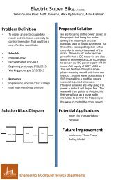

You also want an ePaper? Increase the reach of your titles
YUMPU automatically turns print PDFs into web optimized ePapers that Google loves.
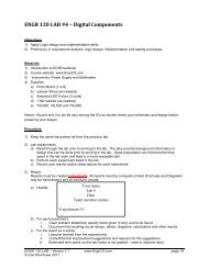
<strong>Digital</strong> <strong>Logic</strong> <strong>Design</strong> <strong>Lab</strong> <strong>#4</strong><br />
Objectives<br />
1) Application of K-map and related design techniques<br />
2) Use of input and output devices in a digital circuit<br />
3) Understanding of basic arithmetic unit design and implementation<br />
4) Proficiency in requirement analysis, logic design, implementation and testing processes.<br />
Materials<br />
1) Textbook: <strong>Digital</strong> <strong>Logic</strong> <strong>Design</strong> by Khormaee.<br />
2) Course Website: www.EngrCS.com<br />
3) Instruments: Power Supply, Function Generator and Oscilloscope<br />
4) Supplies:<br />
a) Proto Board (1 unit)<br />
b) Jumper Wires (as needed)<br />
c) 7-Segment Display (1 unit)<br />
d) 1 kΩ resistor (4 units)<br />
e) 74LSxx as required by the design (consider using BCD to 7-segement driver, 74LS47)<br />
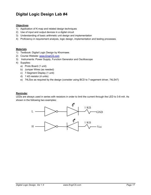
Reminder<br />
LEDs are always used in series with resistors in order to limit the current through the LED to 3-8 mA. As<br />
shown in the following two examples:<br />
L<br />
1KΩ<br />
GND<br />
H<br />
1KΩ<br />
Vcc<br />
<strong>Digital</strong> <strong>Logic</strong> <strong>Design</strong>, Ver 1.4 www.EngrCS.com Page 17
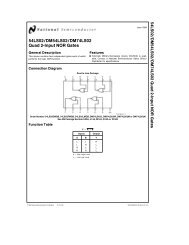
Experiment #1. 7-Segment <strong>Design</strong><br />
7-Segment displays as the name implies have seven segments that may be turned on individually to form an<br />
approximation to a given letter or number. Below are the specifications for Common Anode 7-Segrment<br />
model # Lumex LDS-A304RI:<br />
Pin 1<br />
Pin 14<br />
Pin 7<br />
+<br />
+<br />
+<br />
+<br />
F<br />
E<br />
A<br />
G<br />
D<br />
B<br />
C<br />
+<br />
+<br />
+<br />
+<br />
Packaging Configuration<br />
Pin 8<br />
Limit of Safe Operation<br />
Peak I f < 150 mA<br />
Steady If < 30 mA<br />
Power < 105 mW<br />
Typical<br />
5 mA at 5V<br />
Functional Diagram<br />
It is important that you add a 1 KΩ resistor between Pins 3,14 and Vcc to limit the maximum current through<br />
the diodes. For this experiment:<br />
1) Calculate the maximum combined forward current through all 8 diodes.<br />
Notes:<br />
a) Anode pins (3 &14) are connected to the Vcc through a 1 K resistor.<br />
b) Assume LED have 0 ohm resistor and remember V=I*R where V is voltage in Volts, I is current in<br />
Amps and R is resistance in Ohms.<br />
2) <strong>Design</strong> and Draw the schematic for a circuit that turns on A, B, C, E, F, G segment.<br />
3) Implement your design and document your observations.<br />
<strong>Digital</strong> <strong>Logic</strong> <strong>Design</strong>, Ver 1.4 www.EngrCS.com Page 18
Experiment 2. 2-bit Adder<br />
<strong>Design</strong> a 2-bit binary adder with carry. Your circuit should allow for two 2-bit binary input (a 1 a 0 & b 1 b 0 )<br />
through switches and display the results of the addition in decimal format using the 7-segment display.<br />
Your deliverables include:<br />
a) Clearly identified independent variables (input) and dependent variables (output) for the 2-bit binary<br />
adder system.<br />
b) Truth Table for the system based on input/output defined in part a<br />
c) Write the minimize output functions in either POS or SOP using K-map. Clearly state the literal count and<br />
corresponding number of gates to implement each of the minimized output functions.<br />
d) Using the results from part c or your research into possible designs, draw a schematic to implement 2-bit<br />
adder with carry.<br />
Hint: Consider using Full-adder and half-adder design.<br />
e) Implement, test and demonstrated your design from section d.<br />
Report Requirements<br />
All reports must be computer printed (Formulas and Diagrams may be hand drawn) and at minimum include:<br />
For each Experiment<br />
a) Clear problem statement; specify items given and to be found.<br />
b) Identify the theory or process used.<br />
c) Documents resulting system diagram, schematics, tables, timing diagram, schematic and other<br />
relevant results.<br />
For the report as a whole<br />
a) Cover sheet with your name, course, lab, date of completion and team members’ names.<br />
b) Lessons Learned from the experiments.<br />
c) A new experiment and expected results which provide additional opportunity to practice the concepts<br />
in this lab.<br />
<strong>Digital</strong> <strong>Logic</strong> <strong>Design</strong>, Ver 1.4 www.EngrCS.com Page 19