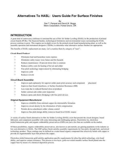
Alternatives To HASL: Users Guide For Surface Finishes - DDM ...
Alternatives To HASL: Users Guide For Surface Finishes - DDM ...
Alternatives To HASL: Users Guide For Surface Finishes - DDM ...

You also want an ePaper? Increase the reach of your titles
YUMPU automatically turns print PDFs into web optimized ePapers that Google loves.
<strong>Alternatives</strong> <strong>To</strong> <strong>HASL</strong>: <strong>Users</strong> <strong>Guide</strong> <strong>For</strong> <strong>Surface</strong> <strong>Finishes</strong><br />
By<br />
Dan T. Parquet and David W. Boggs<br />
Merix Corporation, <strong>For</strong>est Grove, OR<br />
INTRODUCTION<br />
A great deal of controversy continues to surround the use of Hot Air Solder Leveling (<strong>HASL</strong>) in the production of printed<br />
circuit boards (PCBs). The financial burden, technological limitations and environmental issues surrounding the <strong>HASL</strong><br />
process continue to grow. This requires an in-depth review by the printed circuit board manufacturing plant, as well as the<br />
assembly operation and instrument designers ( OEMs), to determine what alternative surface finishes are appropriate.<br />
The benefits of <strong>HASL</strong> replacement are many. Let’s examine them by category of “user”:<br />
Circuit Board Producer<br />
?? Eliminates lead and hazardous waste expense<br />
?? Eliminates safety issues: toxic fumes and fire hazards<br />
?? Reduces maintenance: 20 percent down time is common<br />
?? Reduces utility costs for heating of hot air and solder<br />
?? Fine pitch technology improvement by eliminating bridging<br />
?? Improves yield<br />
?? Reduces rework<br />
Circuit Board Assembler<br />
?? Improves pad coplanarity for superior solder paste print accuracy and component placement<br />
?? Improves bare board cleanliness, or <strong>Surface</strong> Insulation Resistance (SIR)<br />
?? Less warp due to reduced thermal stress at producer<br />
?? Solder contrast aids solder joint inspection<br />
?? Reduces opens and shorts (bridging) with fine pitch devices<br />
Original Equipment Manufacturer<br />
?? Improves reliability from minimal copper-tin intermetallic formation<br />
?? Improves circuit density by the elimination of hole compensation<br />
?? Permits device attachment solder volume control<br />
?? Improves fine pitch design ability (removes board level <strong>HASL</strong> issues)<br />
A variety of surface finish alternatives to Hot Air Solder Leveling (<strong>HASL</strong>) exist that present the circuit designer, board<br />
fabricator, and component assembler with some interesting and challenging options. Electrolytic tin, electroless<br />
nickel/immersion gold, and organic solderability preservatives (OSPs) are just a few that are available on the market.<br />
Of these possibilities, organic solderability preservatives, also known as anti-tarnish, are gaining popularity in the industry as<br />
low cost alternative to <strong>HASL</strong>. The OSP surface finish satisfies assembly requirements for fine pitch, through hole, and mixed<br />
technology product. These coatings may be defined as a water-based organic compound that selectively bonds with copper to<br />
provide an organometallic layer that protects the copper.<br />
Electroless nickel/immersion gold satisfies application-specific requirements for ultra-fine pitch technology, wire bond<br />
ability, and superior contact resistance. This process is two-layer, gold over nickel metallic surface finish plated onto the<br />
copper base by means of a chemical deposition process.
Pure tin offers a distinct environmental advantage over the traditional lead bearing alloys used as temporary metal etch resists<br />
and final plated surface finishes. Matte tin circuitry is a two-layer, tin over nickel metallic surface finish plated onto the<br />
copper base by means of an electrolytic process.<br />
BACKGROUND<br />
Printed circuit boards requiring component attachment, whether leaded or surface mount technology (SMT), must have the<br />
exposed copper land areas coated with a protective finish. This protective coating must be solderable and, at the same time,<br />
act as a barrier for preventing the copper from oxidizing which causes assembly problems for the end user. In the United<br />
States, the predominant surface finish in the PCB industry is <strong>HASL</strong>. Driven by the push for Solder Mask Over Bare Copper<br />
(SMOBC), <strong>HASL</strong> was born as a reliable method to apply solder to the copper surfaces after solder mask. A thin layer of<br />
eutectic solder is deposited onto the exposed copper by passing the boards through a hot, molten wave (or pot) of solder and<br />
subsequently blasting the excess solder from the boards using high velocity hot air. This process is currently under scrutiny<br />
due to environmental and safety issues (hazardous waste/lead exposure), technological limitations (fine-pitch device<br />
assembly), and equipment maintenance expenses to name a few.<br />
In contrast, the alternative processes are environmentally friendly, some provide a surface planarity equivalent to the plated<br />
copper finish, and most require very low equipment maintenance.<br />
Organic Solderability Preservatives (OSP, Anti-tarnish)<br />
Of the OSP compounds, the two that are predominant in the industry are benzotriazole and substituted benzimidazole. The<br />
former of these has been utilized both in the metal finishing industry as a true anti-tarnish for hardware plating, and to a<br />
lesser degree, in the electronics industry for limited heat cycle solder applications on bare copper. The more recently<br />
developed<br />
substituted benzimidazole compounds have the advantage of withstanding multiple heat cycles typically found in mixed<br />
technology PCB assembly operations (surface mount and through hole soldering). This advantage is primarily due to the<br />
coating thickness that is achieved with the substituted compounds, ranging from 5 to 20 microinches 1 (0.1 - 0.5 microns), as<br />
compared to only a monomolecular layer formed with the benzotriazole materials.<br />
In general, OSPs are considered the low cost, high volume alternative, particularly when applied to surface mount technology<br />
due to the excellent surface coplanarity of pads. The cost advantage of the process becomes quite apparent to the board<br />
fabricator. <strong>For</strong> example, facilities and maintenance expenses are only a fraction of the operating cost for the anti-tarnish<br />
process as compared to <strong>HASL</strong>. The process does not involve heating and delivering the high volume air or maintaining a<br />
molten pot of solder. Losses due to rework and rejected product from the <strong>HASL</strong> process are substantial and prevent a<br />
decrease in the cost of manufacturing. An OSP application system eliminates this waste and allows for flexibility to pass the<br />
savings on to the customer.<br />
The cost advantage to the assembler lies primarily in the yield improvements of the component attachment process. <strong>Surface</strong><br />
mount pad planarity is a technical hurdle that <strong>HASL</strong> will never overcome, especially for fine pitch devices due to the extreme<br />
variation in coating thickness. This non-uniform solder thickness can range from 30-1500 microinches (0.75 - 37.5 microns)<br />
depending upon pad geometry and orientation within the panel. In contrast, an OSP coated board provides a surface finish<br />
topography equivalent to the plated copper. This allows for improved component placement; furthermore, it will help move<br />
the assembler towards finer pitch devices and denser circuits as the limiting factor for fine pitch assembly now becomes the<br />
ability to deposit the solder paste.<br />
It must be emphasized that implementing an OSP process may require a re-characterization of the assembly operation; a<br />
number of issues must be addressed. <strong>For</strong> example, the number of thermal cycles a product may see in the assembly process<br />
can reduce the operating window for soldering. If excessive, it may be determined that soldering in an inert atmosphere is<br />
required in the reflow process, wave solder, or both. Typically, OSP suppliers advertise up to five thermal cycles can be<br />
achieved in open air without detrimental effects to solderability. Developing a partnership with the board shop and supplier is<br />
an important consideration during the implementation phase.
A second assembly process consideration when using OSP technology surrounds the type and activity of the flux used in<br />
each of the assembly operations. Table 1 illustrates the results of an engineering evaluation used to benchmark OSPs in<br />
comparison to <strong>HASL</strong> coated PCBs at one customer site. It was apparent in the evaluation that the OSPs performed differently<br />
depending upon the type of flux used. A wide range of responses were found spanning from excellent surface mount<br />
solderability with OA or RMA type solder pastes, to relatively poor filling of holes with a low solids (2%) no clean wave<br />
solder flux that was not designed for soldering to OSP coated pads.<br />
Assembly Operation<br />
SMT Paste<br />
Flux Type<br />
Wave Solder<br />
Flux Type<br />
Results with OSP<br />
Customer ‘A’<br />
Organic Acid<br />
(OA)<br />
Organic Acid<br />
(OA)<br />
Compatible with<br />
all processes<br />
Customer ‘B’<br />
Active Rosin<br />
(RMA)<br />
No Clean<br />
(2% solids<br />
Compatible with SMT process, Alternative<br />
No Clean<br />
wave flux required<br />
Customer ‘C’<br />
Active Rosin<br />
(RMA)<br />
Organic Acid<br />
(OA)<br />
Compatible with<br />
all processes<br />
Customer ‘D’ N/A No Clean<br />
(2% solids)<br />
Alternate No Clean wave flux required<br />
Table 1<br />
At the OEM level, the three key attributes that OSP technology provides the designer are solder joint reliability, circuit<br />
density latitude, and the ability to engineer solder joints.<br />
A standard <strong>HASL</strong> design rule, which is used in the tooling of PCBs, is to oversize drilled holes by 0.002" - 0.003" (50 - 150<br />
microns) to compensate for the reduction in hole diameter caused by the non-uniform <strong>HASL</strong> solder deposit. With the use of<br />
an OSP, this compensation is not necessary; it allows for a reduction of pad size and an overall increase in circuit density.<br />
Additionally, since good solder wetting occurs only where the flux comes into contact with the OSP coated copper pad, the<br />
flow characteristics of the solder are more controlled. This reduces the risk of bridging and provides the possibility for<br />
predicting final solder volume.<br />
Electroless Nickel/Immersion Gold<br />
Electroless nickel is well known in the metal finishing industry for its wide range of physical properties 2 . Hardness, wear<br />
resistance, corrosion resistance and minimal magnetic properties in addition to the high degree of deposit uniformity have<br />
made it a premier metal finish satisfying a wide variety of applications. Geometry’s with almost any degree of complexity<br />
may be plated with electroless nickel, which is an attractive feature allowing for its entry into circuit board applications.<br />
Nickel is also a fairly active metal and quickly passivates (oxidizes) soon after plating, thus soldering to the surface becomes<br />
increasingly difficult with time. However, it has been found that if the nickel is coated with a thin deposit of immersion gold<br />
directly after plating, the solderability will be retained.<br />
Electroless nickel is an auto catalytic process using a precious metal catalyst and internal reducing agent for continuous<br />
deposit as long as the chemistry is maintained in an active state. During the chemical reaction, a small amount of phosphorus<br />
is co-deposited into the nickel creating the desired properties as previously mentioned. Due to the nature of the electroless<br />
process, the nickel deposit may be engineered to a variety of specified thicknesses, but deposits of 100 - 200 microinches (2.5<br />
- 5.0 microns) are typical.<br />
In contrast, immersion gold is deposited in an exchange reaction. As the nickel plated part is introduced into the gold<br />
solution, a chemical exchange occurs replacing nickel on the surface with a thin layer of pure gold. The reaction stops when
all of the exposed nickel is replaced with gold, thus an upper limit of approximately 8 microinches (0.2 microns) is found<br />
with the process.<br />
While obviously a more complex coating method than OSP, the advantage of the electroless nickel/immersion gold process is<br />
an application specific technology on circuit boards. These include PCBs which require excellent solderability on fine pitch<br />
SMDs, corrosion resistance for on-board contact pads, and the opportunity for wire bonding of ultra fine pitch (i.e. 0.008”)<br />
chip on board (COB) designs.<br />
There are some drawbacks which the user should be aware of when considering this finish. Of most concern, due to the<br />
nature of the fairly aggressive chemical process involved, not all solder masks are capable of withstanding the plating baths.<br />
It is desirable to plate after the solder mask application to minimize the gold area plated and provide a “solder mask over bare<br />
copper” (SMOBC) product, but those masks which are high in acrylic content should be applied after the immersion gold<br />
plating. Most liquid photoimageable solder resists with higher epoxy content should be able to withstand the chemical<br />
exposure without evidence of lifting or bath leaching, but these should be tested to verify compatibility.<br />
Matte Tin<br />
Tin plating has been used at Tektronix as a final solderable metal finish for many years, for both aesthetic purposes and a<br />
reliable lead free alternative. Through multiple imaging and plating steps, it allows for complex internal gold contact patterns<br />
to be made as well as surface mount and though hole circuitry. The standard thickness of the tin is 300 to 400 microinches<br />
(7.5 - 10 microns), but this may be tailored to any desired thickness or fine pitch line width as the deposit is not reflowed<br />
after the plating operation.<br />
Nickel provides a copper migration barrier layer and a physical "shelf" for tin to prevent leaf and potential shorts. Plated tin is<br />
more familiar to the PCB industry as a temporary metal etch resist when producing bare copper product and has recently<br />
gained a certain popularity in chemical processing due to the lead free effluent, improved aspect ratio capability, and lack of<br />
stripping residues.<br />
When considering this option, it is important to understand there are different tin deposits available in the industry. Two<br />
popular choices are the matte finish and the bright finish. Bright tins are typically the most aesthetic in appearance, but have a<br />
high degree of codeposited organics and can result in occasional difficulties with dewetting during the soldering operation.<br />
An additional drawback with bright tin is the plating chemistry is not as controllable as the matte tin; therefore, it has less<br />
plating capability at higher aspect ratios (ratio of board thickness-to-hole diameter) greater than 3:1. In general, the matte tin<br />
system provides an improved ability for high aspect ratio plating, fine pitch product coverage, and acceptable performance<br />
for soldering.<br />
Assembly Considerations<br />
Each of these alternate coatings work well with most assembly processes; although, some special considerations must be<br />
taken with the OSP surface finish. It is the mechanism of (acid) fluxing plus heat during the assembly process that dissolves<br />
the organic coating. Good solderability is achieved where flux comes into direct contact with the copper surfaces to be<br />
soldered; hence, screen print and wave solder process optimization may be required.<br />
Another industry perception surrounding OSP technology deals with no clean, low solids flux technology. Contrary to some<br />
reports, OSP coated PCBs can be assembled in an open air environment using no clean, low solids flux technology. This<br />
includes the ability to assemble mixed technology product without the use of an inert atmosphere in the reflow or wave solder
operation. As depicted in Graph 1, some no clean wave solder fluxes perform better than others. It is recommended to<br />
evaluate several no clean fluxes for process compatibility before full production implementation. It must also be mentioned<br />
that, as seen with other finishes such as <strong>HASL</strong>, the use of nitrogen in any assembly process will provide a larger process<br />
window.<br />
Percent Good<br />
(>= 75% Fill)<br />
120<br />
100<br />
80<br />
60<br />
40<br />
20<br />
0<br />
HOLE FILL vs FLUX SUPPLIER<br />
(> 0.020" dia.)<br />
0 1 2 3<br />
Number Thermal Excursions<br />
4<br />
Prior to Wave Solder<br />
FLUX 'A'<br />
FLUX 'B'<br />
FLUX 'C'<br />
GRAPH 1: No Clean (LSF) Flux vs. Thermal Cycling<br />
Another open air test comparing OSP against electroless nickel/immersion gold indicated very similar results. This test<br />
compared hole fill quality of 0.013 inch, O. 023 inch and 0.033 inch diameter holes using a water soluble (OA) wave solder<br />
flux. Test samples were thermally cycled one (1), two (2), and four (4) times prior to the wave solder operation. All samples<br />
passed the 75% solder rise hole fill criteria.<br />
Board washing between assembly operations is another consideration for PCBs coated with an OSP. Aggressive surfactants<br />
or solvents such as Terpenes can actually remove the organic coating. Where cleaning between assembly operations is truly<br />
necessary, it is recommended to use water less than 140?F. If a surfactant is deemed necessary, choose one that is compatible<br />
with organic coatings. Along the same lines, reworking boards from solder paste misprints may also require cleaning.<br />
Rework capability depends upon the rework cleaning process, time delay between cleaning and re-print, and especially, the<br />
assembly process and fluxes used. More active fluxes will typically give better results. It should also be pointed out that the<br />
contrast of the OSP coated copper-to-solder paste interface is much better than <strong>HASL</strong>. This helps to reduce misprints caused<br />
by poor visual alignment of the stencil to the PCB. Additionally, OSP coated boards, unlike <strong>HASL</strong>, are easily reworkable by<br />
the PCB shop; therefore, the assembler can have a fresh coating applied to the PCB whenever the coating is damaged or if<br />
shelf life becomes an issue.<br />
As a final note, in the case where the circuitry is plated with tin, reflow under the solder mask during wave or infrared reflow<br />
is possible if the temperatures are not properly controlled. The melting point of pure tin is 232 °C as compared to 183 °C of<br />
eutectic solder, thus the window is larger than plated solder circuitry but should be nonetheless taken into consideration.<br />
Electrical Contact Considerations<br />
An area that is not adequately discussed in most publications deals with the performance of alternative surface finishes in<br />
electrical contact applications. Electrical testing of bare boards and effects of non-solder coated PCB mounting holes utilized<br />
for grounding purposes need to be taken into consideration in the design and selection process. <strong>For</strong> example, in the case of<br />
OSP, even though the coating is applied to a clean bare copper surface, the organic coating has an insulating property.<br />
Additionally, since the copper will oxidize, steps must be taken to accommodate for this. The following areas are affected by<br />
this phenomenon:
At the PCB Plant:<br />
Continuity electrical test should be performed before the coating process so as not to damage the finish while probing the<br />
surface pads with a “flying lead” or a “bed of nails” test fixture. Oxides on the copper pads created by previous baking<br />
processes may interfere with proper contact, thus a chisel point pin for electrical test is recommended.<br />
At the Assembly Plant:<br />
Circuit grounding relying on mounting hardware is occasionally used in instrument assembly for grounding the PCB to the<br />
chassis or stand-off posts. If the grounding pads are OSP coated copper, it may require a higher torque or more contact<br />
screws to make an adequate ground. This phenomenon may be especially evident during functional testing of the assembled<br />
boards. Depending upon the board design, electrostatic discharge (ESD) pads and other electrical test pads may be effected.<br />
One solution is to screen these surface areas with solder paste, thus becoming solder coated during the reflow process.<br />
At the Instrument Level:<br />
Electromagnetic interference, or EMI shielding, may be effected if the grounding issue is overlooked. During Merix’ OSP<br />
introduction phase, a PCB design issue became apparent on product utilizing plated through holes for mounting and<br />
grounding purposes. The concern related to potential problems surrounding dissimilar metals between the now copper<br />
mounting holes and the plated hardware. These plated through holes are typically masked prior to the wave solder operation<br />
to prevent the holes from plugging with solder. This process leaves the mounting holes with bare copper. A new grounding<br />
hole design that provided a non-plated through hole for mounting and grounding was developed (illustration 1). This design<br />
provides minimal exposed copper without plugging the mounting hole during wave solder. A second benefit from this design<br />
is the elimination of the temporary mask operation prior to wave soldering. Another solution, depending upon the mounting<br />
hardware, would be to selectively gold plate the mounting holes. This only requires an artwork modification on product<br />
already using the selective plate process.<br />
Illustration 1<br />
In regards to electroless nickel/immersion gold, an electromechanical property that is not typically taken advantage of, is the<br />
excellent contact resistance and environmental characteristics of this deposit. In circuit designs which incorporate both the<br />
requirements of high density surface mount assembly and on-board contacts, or compliant pins, this finish is the appropriate<br />
choice. It is generally thought that since the immersion gold is so thin, the surface would not withstand multiple contact<br />
excursions. <strong>To</strong> test this assumption, an experiment was designed with an independent laboratory utilizing spring loaded<br />
spherical type contacts with a normal load force of 100-180 grams. Each contact assembly was connected together in series to<br />
form four electrical “nets” from which resistance measurements could be made. The contact assembly was then cycled 1000<br />
times with periodic resistance measurements and examined via scanning electron microscopy for indication of wear. Contact<br />
resistance results are shown in graph 2.<br />
The results indicate with this type of contact design, a 0.5-1.5% total change in resistance (equivalent to 8-30 milliohm per<br />
contact) may be expected utilizing the electroless nickel/immersion gold finish. The surface exhibited minimal wear with the<br />
gold deposit still intact after cycling. In addition, when the assembly was subjected to environmental testing utilizing the IPC-<br />
TM-650 test method (25-65 C @ 95% RH) with 10 day exposure, it was found that the finish also provided an excellent<br />
barrier layer for corrosion.<br />
A final consideration with electrical contacts is the question of whether the design requires flexibility in lead contact areas.<br />
Flex circuits occasionally have leads which have the substrate removed from all sides and are soldered en-masse with either<br />
hot bar reflow or solder pre-forms.<br />
These “flying lead” designs require a certain amount of bending to allow for uniform bonding to the planar pad arrays. In this<br />
case, electroless nickel/immersion gold is a poor choice as the percent of elongation of the nickel less than 1%. This lack of
ductility will create cracks in the nickel when bent and possibly adhesion failure to the central copper conductor. A more<br />
appropriate choice for this application is the OSP coating.<br />
2<br />
Electroless Nickel/Immersion Gold<br />
Contact Resistance Test Results<br />
% Change (Ohms)<br />
1.5<br />
1<br />
0.5<br />
0<br />
-0.5<br />
0<br />
20<br />
40<br />
60<br />
80<br />
100<br />
120<br />
150<br />
200<br />
400<br />
600<br />
800<br />
1000<br />
GROUP 1<br />
GROUP 2<br />
GROUP 3<br />
GROUP 4<br />
Number Cycles<br />
GRAPH 2: Electroless Nickel/Immersion Gold Contact Resistance<br />
High Frequency Considerations<br />
In microwave structures, the signal loss of the conductor with its associated surface finish must be considered in conjunction<br />
with circuit design. The selection of a surface finish is not as critical for the electrical performance of internal microwave<br />
structures, such as striplines and embedded microstrip designs, due to the minimal interactions of the signals with the surface<br />
finish. <strong>Surface</strong> finish selections for external microwave structures can influence the electrical performance of the system.<br />
Edge coupled structures, such as couplers, coupled line filters, etc. will be influenced the greatest. Signal frequency and line<br />
width and spacing tolerances will also effect the selection of surface finishes for external structures. Higher frequencies<br />
results are smaller skin depths and a greater portion of the signal residing in the outer portions of the signal feature.<br />
Experience at Merix indicates that at frequencies greater than 2 GHz, the extra losses from the electroless nickel can be<br />
excessive in some edge coupled structures. <strong>For</strong> tight tolerance line widths and line spacing structures, the thickness of the<br />
surface finish will be critical and require size compensation of the underlying signal feature. In this case, the tight line width<br />
and spacing tolerances favor the OSP coating.<br />
Reliability Considerations<br />
The October Project Committee 3 has been active in evaluating OSP technology as a viable, alternative surface finish to<br />
<strong>HASL</strong> as it is the only non-metallic surface finish available. Through a series of reliability evaluations by committee<br />
members, it was concluded that organic coatings meet the technical and reliability requirements of the industry. <strong>For</strong> example,<br />
Digital Equipment Corporation and Battelle performed a study to determine the reliability of bare copper versus solder coated<br />
boards 4 . This investigation examined the failure mechanism of metal migration under bias using fine-line technology<br />
product. Conclusion was that bare copper boards are more reliable than solder down to a 0.004” inch line and space.<br />
The presence of exposed copper after the assembly operation is another topic of discussion when dealing with OSP<br />
technology. As with most soldering operations, a 100% wetting of the base metal does not always occur, regardless of the<br />
surface finish selection. This is difficult to visually observe with <strong>HASL</strong> coated product, but contrasting base metals will show<br />
this condition, such as OSPs. The phenomenon will be mostly visible along the perimeter of SMT pads and topside (annular<br />
ring) of plated through holes after wave soldering. As many OEM users have demonstrated, this exposed copper does not<br />
pose any reliability problems. Copper forms a protective oxide layer (like aluminum) which does not continue to decompose.<br />
PCBs have been produced for many years with electrolytic gold or tin as the surface finish, and all contain a significant
amount of exposed copper. The only difference is the copper cannot be readily observed as it is located on the circuit<br />
sidewalls, and not the surface.<br />
In the assembly operation utilizing the electroless nickel/immersion gold, the concern may arise regarding joint embrittlement<br />
which could affect the reliability of the solder connection to the device. In typical applications where solder paste stencils<br />
apply between 0.006” to 0.010” thick solder paste, the volume of immersion gold (3-8 microinches) is not significant as<br />
compared to the volume of solder being deposited. Currently, this surface finish is widely used in telecommunication<br />
applications around the world.<br />
Electrolytic tin plating surface finish has been available for many years. Occasionally, the concern of "tin whiskers" arise<br />
which has caused some apprehension for using pure tin and has actually been rejected by some companies. This<br />
phenomenon, while not completely understood, is often associated with areas of high plating stress and occurs before<br />
soldering operations. At Merix, tin whiskers have been a rare occurrence, in fact, the last reported incident was in the early<br />
1980's from a ten year old bare circuit board plated with bright tin that was found in the warehouse. <strong>To</strong> our knowledge, no<br />
product that has gone through the soldering process has exhibited whiskers with either the bright or matte tin plated finish.<br />
Gold Wire Bond Considerations<br />
Ultra-high density packaging designs occasionally have the requirement for direct die attach and chip on board (COB)<br />
assembly. This combination of fine pitch bond-out leads and need for surface co-planarity excludes the solder, organic, and<br />
tin surface finish options. Traditionally, this requirement has been satisfied by electrolytic pure gold plating in the 30 to 50<br />
microinch range. However, this thickness requirement for wire bonding can be at odds with surface mount device attachment<br />
reliability due to an increase in tin/gold intermetallic solder joint embrittlement.<br />
In an independent study 5 which evaluated gold wire ball bonding, wire pull tests were performed to determine the bond<br />
strength to the immersion gold plating. In the test, 0.001” (25 micron) American Fine gold wire (EL3-6%, T.S. 8 grams) was<br />
used with bond temperature set at 160 degrees C. Results are depicted in table 2. Wire bond data for electroless<br />
nickel/immersion gold shows that this surface finish is a viable option to the traditional electrolytic pure gold plating.<br />
Nickel<br />
Thickness (? m)<br />
Gold<br />
Thickness (? m)<br />
Average Bond<br />
Strength (grams)<br />
Minimum<br />
Bond<br />
(grams)<br />
Standard<br />
Deviation<br />
Percent<br />
Standard<br />
Deviation<br />
4 0.10 6.56 6.3 0.24 4%<br />
7 0.10 5.46 5.0 0.30 5%<br />
4 0.15 7.59 6.9 0.40 5%<br />
7 0.15 7.29 6.6 0.40 6%<br />
Table 2<br />
Cost Considerations<br />
An economic consideration in the selection of alternative surface finishes is the manufacturing cost of the bare printed circuit<br />
board. An operational cost analysis was recently completed at Merix Corporation detailing the annual expenses associated<br />
with the <strong>HASL</strong> process 6 . Many factors were incorporated in this comprehensive study that may not have been included with<br />
a traditional operational cost analysis. During the course of the investigation, a number of "hidden" items and tasks were<br />
found to be necessary in order to support the <strong>HASL</strong> process; but not all were included in the normal operating cost.
These hidden items accounted for an additional 42% in costs which normally would not have been captured in the traditional<br />
cost analysis. <strong>For</strong> example, the cost of materials and labor associated with masking and cleaning selectively gold-plated<br />
contacts was found to be a major expense. Exposed gold circuitry must be masked prior to processing through the <strong>HASL</strong> line<br />
in order to prevent the gold from dissolving into the molten solder bath. The method for subsequently removing this mask is<br />
equally, if not more, labor intensive. Another example not included is the additional cleaning that is often required by PCBs<br />
coated with a dry film solder mask. These masks typically absorb ionic contaminates introduced by the <strong>HASL</strong> process (flux<br />
& oils), thus requiring an added cleaning operation to satisfy surface insulation resistance (SIR) specifications.<br />
A relative cost comparison of the alternative finishes is summarized in the following “Design Selection” chart.<br />
DESIGN SELECTION CHART<br />
Comparison <strong>HASL</strong> OSP IMMERSION<br />
GOLD<br />
MATTE TIN<br />
<strong>Surface</strong><br />
Co-planarity<br />
Poor Best Best Good<br />
Hole Compensation<br />
Required<br />
0.002”-0.003”<br />
Not Required Not Required Required<br />
0.002”-0.003”<br />
Fine Pitch Quality<br />
0.020” or less<br />
Poor Best Best Good<br />
<strong>Surface</strong> Contrast<br />
(Assembly)<br />
Poor<br />
solder/solder<br />
Best<br />
solder/copper<br />
Best<br />
solder/gold<br />
Good<br />
solder/tin<br />
Solder Volume<br />
(Assembly)<br />
Not Predictable Predictable Predictable Predictable<br />
Environmental<br />
Hazard<br />
High<br />
(Pb)<br />
Low<br />
(Water based)<br />
Medium<br />
(Ni)<br />
Medium<br />
(Ni)<br />
Thermally Stressed Yes No No No<br />
Electrical Contact<br />
Use<br />
Fair Poor Good Fair<br />
PCB ShopGold<br />
Contact Masking<br />
Yes<br />
(Difficult)<br />
Not<br />
Required<br />
Not<br />
Possible<br />
Selective Plate<br />
Possible<br />
Grounding<br />
Insulator<br />
No Yes No No<br />
SMOBC Yes Yes Limited No<br />
Reflow under<br />
Solder Mask<br />
No No No Possible<br />
Microwave Fair Best Less than 2GHz Less than 2GHz<br />
Wire Bond No No Yes No
DESIGN SELECTION CHART<br />
Comparison <strong>HASL</strong> OSP IMMERSION<br />
GOLD<br />
MATTE TIN<br />
Shelf Life<br />
(Typical)<br />
12 Months 12 Months<br />
(Process Dependent)<br />
Testing Required<br />
12 Months<br />
Availability Yes Yes Yes Limited<br />
Cost of <strong>Surface</strong><br />
Finish<br />
Standard<br />
(1x)<br />
Lowest<br />
(0.2-0.3x)<br />
Highest<br />
(1.5-2x)<br />
Standard<br />
(0.9-1x)<br />
Chart 1 Process Benefits Comparison<br />
Conclusions<br />
Viable, dependable, and environmentally friendly surface finish alternatives to <strong>HASL</strong> coated PCBs currently exist on the<br />
market. These surface finishes can provide improved assembly performance at a lower total cost. Of the three discussed, the<br />
OSP surface finish is reliable and considered by many to be the high volume, low-cost replacement for <strong>HASL</strong>. While<br />
obviously a more complex coating method than OSP, the advantage which the electroless nickel/immersion gold process<br />
provides is an application specific technology on circuit boards. These include PCBs which require excellent solderability on<br />
fine pitch SMDs, corrosion resistance for on-board contact pads, and the opportunity for wire bonding of ultra fine pitch chip<br />
on board (COB) designs. Matte tin offers a distinct environmental advantage over the traditional lead bearing alloys used as<br />
temporary metal etch resists and final plated surface finishes. It has the additional advantage to allow for complex circuits<br />
with internal gold plated switch contacts without the requirement of masking and subsequent cleaning processes. Other<br />
surface finish options continue to appear, such as electroless or immersion palladium, and are a clear indication that the<br />
industry is moving away from <strong>HASL</strong> towards a more proficient and environmentally friendly alternative.<br />
References<br />
1. Boggs D., “Anti-tarnish: One Alternative to <strong>HASL</strong>”, Electronic Packaging & Production, August 1993<br />
2. Metal Finishing, 1994<br />
3. Payne B., “Copper Protective Coatings Research”, IPC Printed Circuits Expo ‘94 Proceedings, Boston, Massachusetts<br />
1994<br />
4. W. Abbott, “Effects of Operating Environments on Migration of Copper on Printed Circuit Boards”, Digital Equipment<br />
Corporation, 1989<br />
5. Courtesy of Atotech USA, “Application Report Log #5693”,Kulicke & Soffa Industries Inc.,1994<br />
6. Parquet D., Boggs D., “Getting Started With Bare Copper”, SMI Conference and Expo ‘94 Proceedings, San Jose,<br />
California