TRANSISTOR SIZING OF LCD DRIVER CIRCUIT FOR ...
TRANSISTOR SIZING OF LCD DRIVER CIRCUIT FOR ...
TRANSISTOR SIZING OF LCD DRIVER CIRCUIT FOR ...

You also want an ePaper? Increase the reach of your titles
YUMPU automatically turns print PDFs into web optimized ePapers that Google loves.
performance for each<br />
evaluate<br />
with initial driver circuit<br />
combination<br />
constraint<br />
minimize<br />
and choose<br />
violation<br />
smp_diff, area and constraint<br />
minimize<br />
violation<br />
Constraint<br />
violation<br />
Promising<br />
combinations<br />
Stage 3.1<br />
pruning<br />
and choose promising combinations<br />
w/ violation w/o violation<br />
Stage 3.2<br />
promising combinations<br />
pruning<br />
Stage 3.3<br />
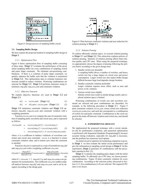
Figure 8: Design process of sampling buffer circuit.<br />
Figure 9: Plots between constraint violation and area reduction for<br />
solution pruning in Stage 3.1.<br />
Area reduction<br />
3.2. Sampling Buffer Design<br />
We here explain the proposed method of sampling buffer design in<br />
Stage 3.<br />
3.2.1. Optimization Flow<br />
Figure 8 shows optimization flow of sampling buffer consisting<br />
of three steps. Stage 3.1 evaluates the performance of the given<br />
initial sampling buffer for every combination of sampling switch<br />
and pulse shape constraint. We eliminate non-promising combinations.<br />
If there is a violation of pulse shape constraint, we<br />
quickly optimize the buffer such that the violation is minimized<br />
in Stage 3.2. This optimization aims to estimate transistor size<br />
increase needed to reduce violation. Promising combinations are<br />
selected for Stage 3.3. Stage 3.3 performs transistor sizing to<br />
minimize smp diif, smp size sum and constraint violation.<br />
3.2.2. Objective Function<br />
We explain objective functions ob j used in Stage 3.2 and<br />
Stage 3.3.<br />
ob j excess sum ´ËØ ¿¾µ (1)<br />
ob j ob j min · excess sum ´ËØ ¿¿µ (2)<br />
Stage 3.2 minimizes constraint violation and Stage 3.3 optimizes<br />
smp diif, smp size sum and constraint violation with a<br />
weighting parameter.<br />
Function excess sum is to compute the sum of constraint violation<br />
of sampling pulse waveform and circuit area, and is expressed<br />
as follows.<br />
excess sum excess´smp dif fµ·excess´smp rµ<br />
· excess´smp f µ·excess´smp wideµ (3)<br />
· excess´smp rto f µ·A¡excess´smp size sumµ<br />
where A is a coefficient to balance violations of waveform constraint<br />
and circuit area constraint. excess is a function to return<br />
constraint violation value, and it returns zero when the constraint<br />
is satisfied.<br />
Function obj min is expressed as a sum of normalized smp diif<br />
and smp size sum with a weighting coefficient size rate.<br />
ob j min <br />
smp dif f<br />
smp dif f u<br />
smp size sum<br />
´1 size rateµ·<br />
¡size rate<br />
smp size sum u<br />
(4)<br />
where 0 size rate 1. smp dif f u and smp size sum u are parameters<br />
for normalization. The coefficient size rate enables tradeoff<br />
analysis between smp diif and smp size sum, and is set by designers<br />
according to the design goal.<br />
3.2.3. Solution Pruning<br />
To explore efficiently solution space, we execute solution pruning<br />
in Stage 3.1 and Stage 3.2. This subsection explains policies of<br />
solution pruning. Intensity of solution pruning affects final solution<br />
quality and CPU time. When using the proposed technique,<br />
we appropriately choose the degree of pruning following the policies<br />
below according to the given design time.<br />
1. Smaller switch size desirable<br />
A sampling buffer drives a number of switches, and hence<br />
switch size has a large impact on circuit area and power<br />
consumption. Larger switch size also makes buffer design<br />
difficult because large load degrades design freedom.<br />
2. Smaller constraint violation preferable<br />
Larger violation requires more effort, such as area and<br />
power, to fix violation.<br />
3. Various switch sizes eligible<br />
Similar switch sizes result in similar design results, and explored<br />
solution space is limited.<br />
Promising combinations of switch size and waveform constraint<br />
are selected and poor combinations are discarded, for<br />
example, in the following procedure in Stage 3.1. Figure 9<br />
plots constraint violation excess sum versus switch size reduction<br />
switch size reduction, and each dot corresponds to a combination<br />
of switch size and pulse constraint. Combinations in the circle are<br />
good in the trade-off between violation and switch size, and should<br />
be selected.<br />
4. EXPERIMENTAL RESULTS<br />
We implemented the proposed technique with a circuit simulator<br />
[6] for performance evaluation, and numerical optimization<br />
is performed with Sequential Quadratic Programming[5], because<br />
accurate timing evaluation, especially for smp diff, is necessary,<br />
and the problem has numerous local optima.<br />
An initial circuit to optimize for technology migration is given.<br />
In Stage 1, we first evaluate the initial circuit performance and<br />
give the information to sampling switch design in Stage 2. In this<br />
experiment, Stage 2 generates 45 combinations with the procedure<br />
reported in Ref. [1].<br />
Stage 3.1 evaluates the sampling pulse shapes with the initial<br />
sampling buffer. To efficiently save CPU time, we choose promising<br />
combinations. Figure 10 plots constraint violation for every<br />
combination. According to the selection policy discussed in Section<br />
3.2.3, five combinations (A-E) are selected. The required CPU<br />
time is two hours.<br />
ISBN 974-94418-9-3 ©2006 ECTI I-27<br />
The 21st International Technical Conference on<br />
Circuits/Systems, Computers and Communications