RF Channel Filtering: a Revival of N-Path Filters in Nanometer CMOS?
RF Channel Filtering: a Revival of N-Path Filters in Nanometer CMOS?
RF Channel Filtering: a Revival of N-Path Filters in Nanometer CMOS?
You also want an ePaper? Increase the reach of your titles
YUMPU automatically turns print PDFs into web optimized ePapers that Google loves.
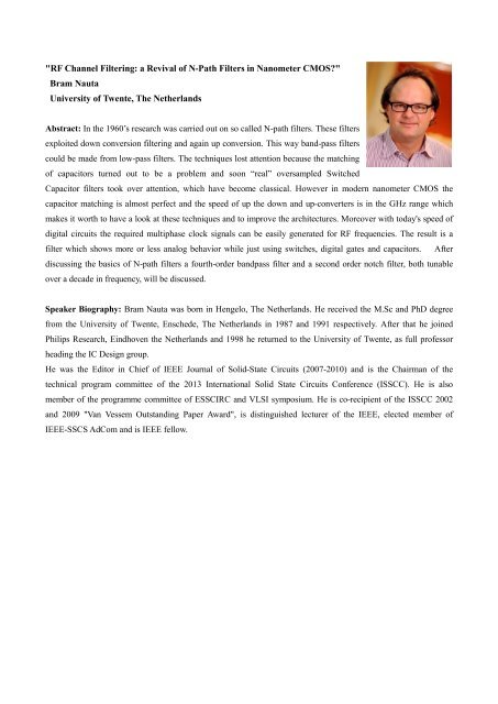
"<strong>RF</strong> <strong>Channel</strong> <strong>Filter<strong>in</strong>g</strong>: a <strong>Revival</strong> <strong>of</strong> N-<strong>Path</strong> <strong>Filters</strong> <strong>in</strong> <strong>Nanometer</strong> <strong>CMOS</strong>?"Bram NautaUniversity <strong>of</strong> Twente, The NetherlandsAbstract: In the 1960’s research was carried out on so called N-path filters. These filtersexploited down conversion filter<strong>in</strong>g and aga<strong>in</strong> up conversion. This way band-pass filterscould be made from low-pass filters. The techniques lost attention because the match<strong>in</strong>g<strong>of</strong> capacitors turned out to be a problem and soon “real” oversampled SwitchedCapacitor filters took over attention, which have become classical. However <strong>in</strong> modern nanometer <strong>CMOS</strong> thecapacitor match<strong>in</strong>g is almost perfect and the speed <strong>of</strong> up the down and up-converters is <strong>in</strong> the GHz range whichmakes it worth to have a look at these techniques and to improve the architectures. Moreover with today's speed <strong>of</strong>digital circuits the required multiphase clock signals can be easily generated for <strong>RF</strong> frequencies. The result is afilter which shows more or less analog behavior while just us<strong>in</strong>g switches, digital gates and capacitors. Afterdiscuss<strong>in</strong>g the basics <strong>of</strong> N-path filters a fourth-order bandpass filter and a second order notch filter, both tunableover a decade <strong>in</strong> frequency, will be discussed.Speaker Biography: Bram Nauta was born <strong>in</strong> Hengelo, The Netherlands. He received the M.Sc and PhD degreefrom the University <strong>of</strong> Twente, Enschede, The Netherlands <strong>in</strong> 1987 and 1991 respectively. After that he jo<strong>in</strong>edPhilips Research, E<strong>in</strong>dhoven the Netherlands and 1998 he returned to the University <strong>of</strong> Twente, as full pr<strong>of</strong>essorhead<strong>in</strong>g the IC Design group.He was the Editor <strong>in</strong> Chief <strong>of</strong> IEEE Journal <strong>of</strong> Solid-State Circuits (2007-2010) and is the Chairman <strong>of</strong> thetechnical program committee <strong>of</strong> the 2013 International Solid State Circuits Conference (ISSCC). He is alsomember <strong>of</strong> the programme committee <strong>of</strong> ESSCIRC and VLSI symposium. He is co-recipient <strong>of</strong> the ISSCC 2002and 2009 "Van Vessem Outstand<strong>in</strong>g Paper Award", is dist<strong>in</strong>guished lecturer <strong>of</strong> the IEEE, elected member <strong>of</strong>IEEE-SSCS AdCom and is IEEE fellow.
"Time-Doma<strong>in</strong> Analog and <strong>RF</strong> Signal Process<strong>in</strong>g"Robert Bogdan StaszewskiDelft University <strong>of</strong> Technology, The NetherlandsAbstract: One <strong>of</strong> the most important developments <strong>in</strong> the wireless <strong>in</strong>dustry with<strong>in</strong> thelast decade was the <strong>in</strong>vention and popularization <strong>of</strong> the time-doma<strong>in</strong> analog/<strong>RF</strong>microelectronics. The new paradigm revolves around a bold premise <strong>of</strong> “the superiority<strong>of</strong> a time-doma<strong>in</strong> operation over the traditional voltage-doma<strong>in</strong> operation” <strong>in</strong> which thetime-stamps, rather than the voltage or current levels, are the <strong>in</strong>formation carrier. This approach works surpris<strong>in</strong>glywell <strong>in</strong> nanoscale <strong>CMOS</strong> processes, be<strong>in</strong>g nowadays the ma<strong>in</strong>stream process technology for consumer electronics,with their ris<strong>in</strong>g and fall<strong>in</strong>g transition times on the order <strong>of</strong> 10 picoseconds as well as extremely low energyconsumption due to the fact that only 100 or so electrons are <strong>in</strong>volved <strong>in</strong> each transition. This new paradigm hasbeen successfully exploited by this author while at Texas Instruments <strong>in</strong> Dallas, Texas, USA, to transform the entirewireless transmitter/receiver architecture <strong>in</strong> which the analog and <strong>RF</strong> circuits operate now <strong>in</strong> the time-doma<strong>in</strong>.Specifically, a time-to-digital converter (TDC) and a digitally-controlled oscillator (DCO), which form anall-digital phase-locked loop (ADPLL), have been proposed to significantly improve the frequency synthesizersoperat<strong>in</strong>g at multi-GHz frequencies. New <strong>in</strong>f<strong>in</strong>ite-impulse response (IIR) filters have been proposed to processweak antenna signals <strong>in</strong> the new discrete-time receiver architecture. This new approach drastically improves cost,area/volume, energy consumption and <strong>in</strong>tegration level <strong>of</strong> analog electronic circuits. Consequently, the majority <strong>of</strong>the 1.6 billion cell phones produced annually are now based on this approach. However, this author believes thatthe time-doma<strong>in</strong> analog revolution has merely begun and the best is yet to come with new aspects (e.g., ultra-lowpower, millimeter-wave), circuits (e.g., ADC, DAC) and applications (e.g., satellite communications; non-wireless,such as 3D imagers) begg<strong>in</strong>g to be exploited. This talk revisits this excit<strong>in</strong>g journey and <strong>of</strong>fers glimpse <strong>of</strong> futuredevelopments.Speaker Biography: R. Bogdan Staszewski received BSEE (summa cum laude), MSEE and PhD from University<strong>of</strong> Texas at Dallas, USA, <strong>in</strong> 1991, 1992 and 2002, respectively. From 1991 to 1995 he was with Alcatel <strong>in</strong>Richardson, Texas. He jo<strong>in</strong>ed Texas Instruments <strong>in</strong> Dallas, Texas <strong>in</strong> 1995. In 1999 he co-started a Digital <strong>RF</strong>Processor (DRPTM) group with a mission to <strong>in</strong>vent new digitally-<strong>in</strong>tensive approaches to traditional <strong>RF</strong> functions.Dr. Staszewski has served as a CTO <strong>of</strong> the DRP group between 2007 and 2009. S<strong>in</strong>ce July 2009 he is AssociatePr<strong>of</strong>essor at Delft University <strong>of</strong> Technology <strong>in</strong> the Netherlands. He has co-authored one book, four book chapters,135 journal and conference publications, and holds 100 issued and 50 pend<strong>in</strong>g US patents. His research <strong>in</strong>terests<strong>in</strong>clude nanoscale <strong>CMOS</strong> architectures and circuits for frequency synthesizers, transmitters and receivers. He is anIEEE Fellow.
"Advanced Digital <strong>RF</strong> MIMO Transceiver for Next Generation MobileCommunication"Hyun-Kyu YuElectronics & Telecommunications Research Institute, KoreaAbstract: The <strong>RF</strong> front-end is the last exempt and barrier to be true digital convergenceon the hand-held phone. Some pioneers dream SDR ideally or try practical digital<strong>in</strong>tensive transceiver such as DRP <strong>of</strong> TI. A new Digital <strong>RF</strong> Transceiver SoC withm<strong>in</strong>imum analog signal process<strong>in</strong>g is <strong>in</strong>troduced. The receiver is composed <strong>of</strong> only three blocks: LNA, DirectDigital Converter (DDC), and external SAW. In the transmitter, the digital baseband signal is directly converted tothe <strong>RF</strong> by Direct <strong>RF</strong> Converter (D<strong>RF</strong>C). Most analog signal process<strong>in</strong>g is done at the Digital Front End (DFE).This novel architecture was applied successfully to the 3G LTE transceiver at the band <strong>of</strong> 2.1GHz with variablebandwidth <strong>of</strong> 1.4/3/5/10/15/20MHz. The design details and implementation results will be presented on the spot.Speaker Biography: Hyun-Kyu Yu received the B.S. and M.S. degrees <strong>in</strong> electronics eng<strong>in</strong>eer<strong>in</strong>g fromKyungpook Nat’l University <strong>in</strong> 1981 and 1983 respectively, and the Ph.D. degree <strong>in</strong> electrical and electronicseng<strong>in</strong>eer<strong>in</strong>g from KAIST <strong>in</strong> 1994. In 1983, he jo<strong>in</strong>ed the ETRI, where he worked on both devices and circuittechnologies on <strong>CMOS</strong>, VDMOS, PSA BJT, 4M/16M/64M DRAM, SOI MOSFET model<strong>in</strong>g, and standard celllibrary. S<strong>in</strong>ce 1996, he has led <strong>RF</strong>/Analog IC design team that successfully developed the world first <strong>CMOS</strong> basedRx/Tx chips for the CDMA and PCS cellular phone <strong>in</strong> 1999 and 2001 respectively. He also directed several tasks <strong>in</strong>the area <strong>of</strong> <strong>RF</strong>IC <strong>in</strong>clud<strong>in</strong>g digital TV tuner, DDFS, IEEE 802.11.a/b, WCDMA handset, Digital MultimediaBroadcast<strong>in</strong>g, and 10Gbps SerDes. S<strong>in</strong>ce 2006, he has been the director <strong>of</strong> <strong>RF</strong> Circuit Group which <strong>in</strong>cludesresearch on mm-wave applications such as 60GHz WPAN and 77GHz/94GHz radar sensor system <strong>in</strong> SiGe and/orcompound semiconductor devices <strong>in</strong>clud<strong>in</strong>g HEMT and HBT. More recently, he worked on Digital <strong>RF</strong> transceiverSoC for mobile TV and 3G LTE application. And he is currently responsible for SW-SoC Convergence Laboratoryas a senior vice president <strong>of</strong> ETRI.Dr. Yu is a board member <strong>of</strong> IEEK and a senior member <strong>of</strong> IEEE. He founded and has been serv<strong>in</strong>g as chairman <strong>of</strong>the <strong>RF</strong> Integrated Circuit Technology Society <strong>in</strong> Korea s<strong>in</strong>ce 2000. He has received several awards <strong>in</strong>clud<strong>in</strong>g Nat’lAward from Government for the contribution to the research on <strong>RF</strong> <strong>CMOS</strong> technologies. He is the author andco-author <strong>of</strong> over 120 technical papers and 100 patents <strong>in</strong> the <strong>RF</strong> devices, circuits, and system design areas.
"Sensor Enabled UHF Passive <strong>RF</strong>ID Tag for Wireless Monitor<strong>in</strong>g Applications"Man-Kay LawUniversity <strong>of</strong> Macau, Ch<strong>in</strong>aAbstract: Passive <strong>RF</strong>ID tags operat<strong>in</strong>g <strong>in</strong> the UHF band compliant to EPC Gen-2 havebeen widely adopted <strong>in</strong> various applications. Comb<strong>in</strong>ed with embedd<strong>in</strong>g sensory systems,various wireless monitor<strong>in</strong>g applications can be readily accomplished. The challenge, however, is the realization <strong>of</strong>ultra-low power sens<strong>in</strong>g with system level optimization to alleviate the potential degradation <strong>in</strong> the tag operat<strong>in</strong>gdistance.We will present a system-on-chip passive <strong>RF</strong>ID tag with an embedded temperature sensor for the EPC Gen-2protocol <strong>in</strong> the 900-MHz UHF band. With system level optimization and co-design<strong>in</strong>g <strong>of</strong> system build<strong>in</strong>g blocks,temperature sens<strong>in</strong>g us<strong>in</strong>g nanowatt additional power consumption can be accomplished. Fabricated <strong>in</strong> a standard0.18-µm <strong>CMOS</strong> process, the 1.1-mm2 tag chip is bonded onto an antenna us<strong>in</strong>g flip-chip technology to realize acomplete tag <strong>in</strong>lay, which is successfully demonstrated and evaluated <strong>in</strong> real-time wireless communications withcommercial <strong>RF</strong>ID readers. The tag <strong>in</strong>lay achieves a sensitivity <strong>of</strong> -6 dBm and a sens<strong>in</strong>g <strong>in</strong>accuracy <strong>of</strong> ±0.8°C (3σ)over operat<strong>in</strong>g temperature range from -20°C to 30°C with one-po<strong>in</strong>t calibration.Speaker Biography: Man-Kay Law received the B.Sc. <strong>in</strong> Computer Eng<strong>in</strong>eer<strong>in</strong>g and the PhD degree <strong>in</strong> Electronicand Computer Eng<strong>in</strong>eer<strong>in</strong>g from Hong Kong University <strong>of</strong> Science and Technology (HKUST), <strong>in</strong> 2006 and 2011,respectively. From February 2011, he jo<strong>in</strong>ed HKUST as a Visit<strong>in</strong>g Assistant Pr<strong>of</strong>essor. He is currently an AssistantPr<strong>of</strong>essor <strong>in</strong> the State Key Laboratory <strong>of</strong> Analog and Mixed-Signal VLSI, Faculty <strong>of</strong> Science and Technology,University <strong>of</strong> Macau. His research <strong>in</strong>terests are <strong>in</strong> the area <strong>of</strong> ultra-low power energy harvest<strong>in</strong>g and sens<strong>in</strong>gcircuits for wireless sens<strong>in</strong>g and biomedical systems, with special emphasis on smart <strong>CMOS</strong> temperature sensors,<strong>CMOS</strong> image sensors, ultra-low power analog design techniques, and <strong>in</strong>tegrated energy harvest<strong>in</strong>g techniques. Hecurrently serves as a member <strong>of</strong> the IEEE Circuits and Systems Society (CASS) technical committee on SensorySystems as well as Biomedical Circuits and Systems.
"Low Power Circuits for Body Area Network (BAN)"Jerald YooMasder Institute <strong>of</strong> Science and Technology, United Arab EmiratesAbstract: We are fac<strong>in</strong>g a new era <strong>of</strong> semiconductor, from technology-driven towardsapplication-driven evolution. Currently, chronic diseases account for over 1/3 <strong>of</strong> deathsaround the world, and to deal with this, healthcare paradigm is shift<strong>in</strong>g from reactive illness management towardsproactive and preemptive health management; the goal here is to ma<strong>in</strong>ta<strong>in</strong> healthy life <strong>in</strong> the first place, or preventillness from gett<strong>in</strong>g any worse by cont<strong>in</strong>uously monitor<strong>in</strong>g health dur<strong>in</strong>g normal daily life.Body Area Network (BAN) is a strong candidate to realize cont<strong>in</strong>uous health monitor<strong>in</strong>g environment. A popularapproach to form a BAN is by adopt<strong>in</strong>g <strong>RF</strong> radio communication; however, <strong>in</strong>terference and security issues limitthe <strong>RF</strong> approach to be the ultimate solution. Wearable BAN can complement the <strong>RF</strong> by us<strong>in</strong>g a conductive channelon fabric or a body channel, and this gives the circuit society a chance to lead another evolution.Speaker Biography: Jerald Yoo received the B.S., M.S., and Ph.D. degrees <strong>in</strong> Department <strong>of</strong> ElectricalEng<strong>in</strong>eer<strong>in</strong>g from the Korea Advanced Institute <strong>of</strong> Science and Technology (KAIST), Daejeon, Korea, <strong>in</strong> 2002,2007, and 2010, respectively.In May 2010, he jo<strong>in</strong>ed the faculty <strong>of</strong> Microsystems Eng<strong>in</strong>eer<strong>in</strong>g, Masdar Institute <strong>of</strong> Science and Technology,Abu Dhabi, United Arab Emirates, where he is an assistant pr<strong>of</strong>essor. Dur<strong>in</strong>g June 2010 to June 2011, he was alsowith Microsystems Technology Laboratory, Massachusetts Institute <strong>of</strong> Technology (MIT), Cambridge, MA, USA,as a visit<strong>in</strong>g scholar. He developed low-energy Body Area Network (BAN) transceivers and wearable body sensornetwork us<strong>in</strong>g Planar-Fashionable Circuit Board (P-FCB) for cont<strong>in</strong>uous health monitor<strong>in</strong>g system. His researchfocuses on low energy circuit technology for wearable bio signal sensors, wireless power transmission, SoC designto system realization for wearable healthcare applications, and energy-efficient biomedical circuits. He is an author<strong>of</strong> the book chapter <strong>in</strong> Biomedical <strong>CMOS</strong> ICs (Spr<strong>in</strong>ger, 2010).Dr. Yoo is a co-recipient <strong>of</strong> the Asian Solid-State Circuits Conference (A-SSCC) Outstand<strong>in</strong>g Design Awards <strong>in</strong>2005. Currently he serves as a technical program committee member <strong>of</strong> Asian Solid-State Circuits Conference(A-SSCC).
"Low-power <strong>RF</strong>IC design for 60GHz system-on-chip applications"Kaixue MA (Speaker) and Kiat Seng YEONanyang Technological University, S<strong>in</strong>gaporeAbstract: Radio Frequency (<strong>RF</strong>) Integrated Circuits (ICs) are crucial circuits formodern wireless communication systems. Prompted by mobile applications such asGSM, 3G, WiFi, WiMAX and LTE, <strong>RF</strong>IC market is fast grow<strong>in</strong>g and very dynamic <strong>in</strong>the IC <strong>in</strong>dustry. However, these mobile applications br<strong>in</strong>g challenges for the <strong>RF</strong>ICdesign with str<strong>in</strong>gent and conflict<strong>in</strong>g constra<strong>in</strong>ts <strong>of</strong> high performance, low power and low cost for mass adoption.There are three major trends for <strong>RF</strong>IC design to cater<strong>in</strong>g for different applications and progresses <strong>of</strong> the standards.Firstly, the operat<strong>in</strong>g frequency is mov<strong>in</strong>g towards higher frequency like 60GHz and beyond. Secondly, theoperat<strong>in</strong>g bandwidth is becom<strong>in</strong>g larger from MHz <strong>in</strong> GSM to several GHz <strong>in</strong> 60GHz radio. Thirdly, the powerconsumption is cont<strong>in</strong>ually reduc<strong>in</strong>g prompted by portable applications. This talk presents recent progress on <strong>RF</strong>ICdesign for low-power 60GHz applications with consideration <strong>of</strong> these three major trends. It will also cover designissues from product def<strong>in</strong>ition to <strong>RF</strong> circuits, SOC design as well as co-design <strong>of</strong> SOC and packag<strong>in</strong>g. Some<strong>in</strong>novative design techniques for VCO, switch, broadband AGC etc, used <strong>in</strong> 60GHz radio will be <strong>in</strong>troduced.Speaker Biography: Kaixue MA received the Ph.D degree from Nanyang Technological University (NTU),S<strong>in</strong>gapore. From 1997 to 2002, he was with Ch<strong>in</strong>a Academy <strong>of</strong> Space Technology (Xi’an), where he was groupleader <strong>of</strong> millimeter-wave group for space-borne microwave and millimeter-wave components and subsystems forsatellite payload. From 2005 to 2007, he was with MEDs Technologies as an R&D Manager. From 2007 to 2010,he was with ST Electronics (Satcom & Sensor Systems) as R&D Manager and Technique Management Committee<strong>of</strong> ST Electronics. He developed Ka VSAT products sell<strong>in</strong>g <strong>in</strong> market for VSAT ground station. S<strong>in</strong>ce March 2010,he is with NTU as a Senior Research Fellow and <strong>RF</strong>IC team leader for 60GHz Flagship Chipset project SOC. AsPI/technique leader, he successfully completed projects with fund more than S$12M (exclud<strong>in</strong>g projects done <strong>in</strong>Ch<strong>in</strong>a). He has applied 7 patents and 3 patents <strong>in</strong> pend<strong>in</strong>g <strong>in</strong> <strong>RF</strong> & millimeter-wave IC design and has authored orco-authored over 90 journal and conference papers. Dr Ma is a Senior Member <strong>of</strong> IEEE.
"A Novel 1TX/4RX 77GHz Radar System <strong>in</strong> 65nm <strong>CMOS</strong> with DigitalBeamform<strong>in</strong>g Technique"Jri LeeNational Taiwan University, TaiwanAbstract: This work presents a 77GHz automotive radar system <strong>in</strong>clud<strong>in</strong>g LTCCantenna and digital beamform<strong>in</strong>g. Fully <strong>in</strong>tegrated <strong>in</strong> 65nm <strong>CMOS</strong> and assembled withflip-chip technique, the radar achieves 100m and +/- 8 degree detection distance andangle, respectively, <strong>in</strong> a t<strong>in</strong>y volume <strong>of</strong> 2.5cm x 4cm x 1cm.Speaker Biography: Jri Lee is Pr<strong>of</strong>essor <strong>of</strong> Electrical Eng<strong>in</strong>eer<strong>in</strong>g at National Taiwan University. His research<strong>in</strong>cludes wireless and wirel<strong>in</strong>e transceivers, high-speed communication systems, and mmwave techniques. He isserv<strong>in</strong>g or has served as SSCS Dist<strong>in</strong>guished Lecturer, TPC members <strong>of</strong> ISSCC, VLSI Symposium, and A-SSCC.He received the Beatrice W<strong>in</strong>ner Award at ISSCC2007 and Takuo Sugano at ISSCC2008.
"60GHz <strong>CMOS</strong> Transceiver Design for Mobile Applications Based onWiGig/IEEE802.11ad Standard"Koji Tak<strong>in</strong>ami (Speaker), Noriaki Saito, Kazuaki TakahashiPanasonic, JapanAbstract: A 60GHz short range wireless system <strong>of</strong>fers new opportunities for achiev<strong>in</strong>gwireless high-def<strong>in</strong>ition video l<strong>in</strong>ks and multi-Gb/s wireless data transfer. Recent workshave realized such a transceiver <strong>in</strong> a cost effective <strong>CMOS</strong> process, but us<strong>in</strong>g a 60GHzsystem <strong>in</strong> mobile term<strong>in</strong>als is extremely challeng<strong>in</strong>g to achieve low power consumption as well as small form factor.This talk addresses design challenge and recent progress <strong>of</strong> 60GHz transceiver developments target<strong>in</strong>g for mobileusage. The talk covers various design techniques such as a transformer-based compact LNA, a small quadraturehybrid, an auto calibrated PLL and etc. With those techniques, a 60GHz direct conversion transceiver is fabricated<strong>in</strong> a 90nm <strong>CMOS</strong> process. The developed transceiver achieves up to 1.76Gsps pi/2-BPSK/QPSK modulation withexcellent distortion and spurious suppression that meet the IEEE802.11ad standard.Short Biography: Koji Tak<strong>in</strong>ami received the B.S. and M.S. degrees <strong>in</strong> electrical eng<strong>in</strong>eer<strong>in</strong>g from KyotoUniversity, Kyoto, Japan, <strong>in</strong> 1995 and 1997, respectively. In 1997, he jo<strong>in</strong>ed Matsushita Electric Industrial(Panasonic) Co., Ltd., Osaka, Japan. S<strong>in</strong>ce then he has been engaged <strong>in</strong> the design <strong>of</strong> analog and <strong>RF</strong> circuits forwireless communications. From 2004 to 2006, he was a visit<strong>in</strong>g scholar at the University <strong>of</strong> California, LosAngeles (UCLA), where he was <strong>in</strong>volved <strong>in</strong> the architecture and circuit design <strong>of</strong> the high efficiency <strong>CMOS</strong> poweramplifier. In 2006, he jo<strong>in</strong>ed Panasonic Silicon Valley Lab, Cupert<strong>in</strong>o, CA, where he worked on high efficiencytransmitters and low phase-noise digital PLLs. In 2010, he relocated to Japan and jo<strong>in</strong>ed Communication CoreDevices Development Center, Panasonic, where he currently leads the development <strong>of</strong> the millimeter wavetransceiver ICs.


