RF Channel Filtering: a Revival of N-Path Filters in Nanometer CMOS?
RF Channel Filtering: a Revival of N-Path Filters in Nanometer CMOS?
RF Channel Filtering: a Revival of N-Path Filters in Nanometer CMOS?
Create successful ePaper yourself
Turn your PDF publications into a flip-book with our unique Google optimized e-Paper software.
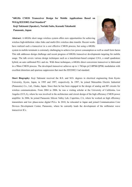
"60GHz <strong>CMOS</strong> Transceiver Design for Mobile Applications Based onWiGig/IEEE802.11ad Standard"Koji Tak<strong>in</strong>ami (Speaker), Noriaki Saito, Kazuaki TakahashiPanasonic, JapanAbstract: A 60GHz short range wireless system <strong>of</strong>fers new opportunities for achiev<strong>in</strong>gwireless high-def<strong>in</strong>ition video l<strong>in</strong>ks and multi-Gb/s wireless data transfer. Recent workshave realized such a transceiver <strong>in</strong> a cost effective <strong>CMOS</strong> process, but us<strong>in</strong>g a 60GHzsystem <strong>in</strong> mobile term<strong>in</strong>als is extremely challeng<strong>in</strong>g to achieve low power consumption as well as small form factor.This talk addresses design challenge and recent progress <strong>of</strong> 60GHz transceiver developments target<strong>in</strong>g for mobileusage. The talk covers various design techniques such as a transformer-based compact LNA, a small quadraturehybrid, an auto calibrated PLL and etc. With those techniques, a 60GHz direct conversion transceiver is fabricated<strong>in</strong> a 90nm <strong>CMOS</strong> process. The developed transceiver achieves up to 1.76Gsps pi/2-BPSK/QPSK modulation withexcellent distortion and spurious suppression that meet the IEEE802.11ad standard.Short Biography: Koji Tak<strong>in</strong>ami received the B.S. and M.S. degrees <strong>in</strong> electrical eng<strong>in</strong>eer<strong>in</strong>g from KyotoUniversity, Kyoto, Japan, <strong>in</strong> 1995 and 1997, respectively. In 1997, he jo<strong>in</strong>ed Matsushita Electric Industrial(Panasonic) Co., Ltd., Osaka, Japan. S<strong>in</strong>ce then he has been engaged <strong>in</strong> the design <strong>of</strong> analog and <strong>RF</strong> circuits forwireless communications. From 2004 to 2006, he was a visit<strong>in</strong>g scholar at the University <strong>of</strong> California, LosAngeles (UCLA), where he was <strong>in</strong>volved <strong>in</strong> the architecture and circuit design <strong>of</strong> the high efficiency <strong>CMOS</strong> poweramplifier. In 2006, he jo<strong>in</strong>ed Panasonic Silicon Valley Lab, Cupert<strong>in</strong>o, CA, where he worked on high efficiencytransmitters and low phase-noise digital PLLs. In 2010, he relocated to Japan and jo<strong>in</strong>ed Communication CoreDevices Development Center, Panasonic, where he currently leads the development <strong>of</strong> the millimeter wavetransceiver ICs.


