UMTS~slash~GSM MULTI MODE RECEIVER DESIGN - Mumor.org
UMTS~slash~GSM MULTI MODE RECEIVER DESIGN - Mumor.org
UMTS~slash~GSM MULTI MODE RECEIVER DESIGN - Mumor.org

You also want an ePaper? Increase the reach of your titles
YUMPU automatically turns print PDFs into web optimized ePapers that Google loves.
➠<br />
➡<br />
UMTS/GSM <strong>MULTI</strong> <strong>MODE</strong> <strong>RECEIVER</strong> <strong>DESIGN</strong><br />
Horst Fischer, Frank Henkel, Michael Engels, Peter Waldow<br />
IMST GmbH, Carl-Friedrich-Gauss-Str. 2, 47475 Kamp-Lintfort, Germany<br />
ABSTRACT<br />
With the objective of designing a transceiver IC for multi<br />
mode operation, the RF requirements for the whole<br />
transceiver from antenna to baseband are derived from the<br />
UMTS- and GSM-standards. The RF-parameters found for<br />
the overall system are broken down to building block<br />
level. The boundary conditions for the transceiver IC were<br />
defined using specifications of currently available external<br />
components. The work presented here focuses mainly on<br />
the receiver design, but in case of UMTS-FDD it also<br />
takes the interference from the transmitter into account.<br />
Multi mode operation of the transceiver could be obtained<br />
by re-using most of the building blocks. Others like front<br />
end SAW-filters can neither be integrated nor re-used.<br />
1. INTRODUCTION<br />
The demand for higher data rates in mobile<br />
communication led to the introduction of third generation<br />
mobile communication systems, often referred to as 3G.<br />
Of course during the start the coverage of 3G networks<br />
will be far from complete. The subscriber who is used to<br />
the good coverage provided by 2G networks will not be<br />
satisfied with less. Hence, during the transition from 2G to<br />
3G the handsets have to be capable of working in both<br />
networks, combining the high data rates provided by 3G<br />
wherever available and the good coverage of 2G<br />
elsewhere. In Europe the according 3G standards are<br />
UMTS FDD and UMTS TDD. The 2G standards are<br />
EGSM and DCS 1800. The RF-aspects are defined in the<br />
according 3GPP and ETSI specifications [1], [2] and [3].<br />
The GSM standard is well established and various chip<br />
sets are available. While the UMTS FDD network is<br />
currently being built up in Europe, TDD is to follow<br />
shortly after, so that multi mode phones and components<br />
become necessary. The RF requirements for the FDD<br />
mode have already been investigated [4]. The work<br />
presented here has its focus on multi mode operation.<br />
2. RF-REQUIREMENTS<br />
Most of the RF relevant parameters can directly be derived<br />
from the GSM- and UMTS-standards. These RF<br />
parameters have to be distributed among the transceiver IC<br />
and external components. Besides that some aspects of<br />
multi mode operation have to be considered.<br />
2.1. UMTS-requirements<br />
For the UMTS FDD and TDD mode a set of receiver test<br />
cases is defined, in which a Bit Error Rate (BER) of 0.001<br />
must not be exceeded. All these test cases use a DL<br />
reference measurement channel (12.2 kbps). The<br />
maximum input power test case for UMTS includes the<br />
presence of an interfering signal that can be regarded as<br />
noise. This interfering signal uses the same frequency but<br />
other spreading sequences and can not be eliminated<br />
before the digital baseband. The linearity requirements<br />
must be met for the interferer plus the useful part, while<br />
the voltage of the desired part of the signal has to be<br />
amplified to the set-point. Since the BER of 0.001 has to<br />
be met for this test case it also yields a Signal to Noise<br />
Ratio SNR that guarantees a BER 0.001.With this SNR<br />
and the minimum input power the required system noise<br />
figure NF can be estimated without detailed analysis of the<br />
baseband algorithms. The Adjacent Channel Selectivity<br />
(ACS) and the in band blocking test case for UMTS<br />
specify the baseband filter characteristic and the phasenoise<br />
performance of the RX-VCO. IIP3 is defined in the<br />
intermodulation test case and IIP2 can be calculated from<br />
the blocking at 15 MHz offset in case of UMTS TDD and<br />
from self blocking in case of UMTS FDD. The RFparameters<br />
listed below in Table 1 refer to the antenna<br />
connector of the user equipment. Instead of power gain the<br />
voltage amplification A V is listed, since the input<br />
impedances of the baseband stages can be in the range of<br />
some M.<br />
SNR min NF max IIP2 min IIP3 min<br />
FDD -18.9 dB 9.6 dB 8 dBm -21.3 dBm<br />
TDD -6 dB 9.2 dB 8 dBm -20.9 dBm<br />
P min P max A V,min A V,max<br />
FDD -117 dBm -25 dBm 22 dB 95 dB<br />
TDD -105 dBm -25 dBm 10 dB 83 dB<br />
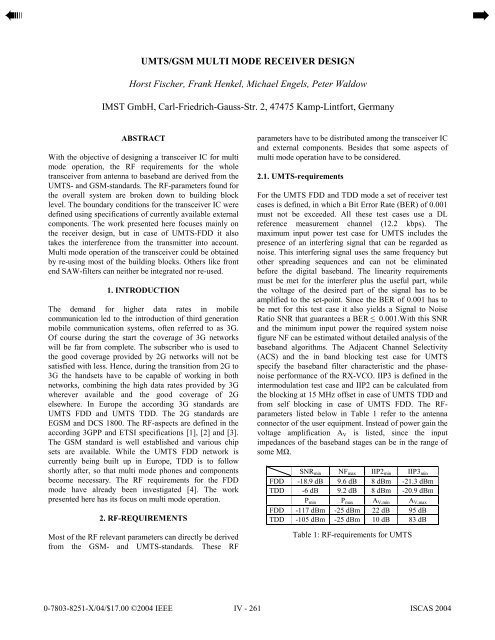
Table 1: RF-requirements for UMTS<br />
0-7803-8251-X/04/$17.00 ©2004 IEEE IV - 261<br />
ISCAS 2004
➡<br />
➡<br />
2.2. GSM-requirements<br />
1<br />
2<br />
3<br />
For EGSM and DCS 1800 some test cases are defined<br />
differently. The cochannel interference test case directly<br />
yields the SNR, that is necessary to achieve the required<br />
BER. The specified Carrier to Interferer Ratio CIR = 9 dB<br />
is the same as the required SNR for most of the other test<br />
cases. IIP2 is calculated from the AM suppression<br />
characteristics. System noise figure NF, VCO phase-noise,<br />
IIP3, and filter performance are calculated similar to their<br />
UMTS-equivalents. The RF-parameters for EGSM and<br />
DCS 1800 are listed in Table 2. They also refer to the<br />
antenna connector of the device.<br />
SNR min NF max IIP2 min IIP3 min<br />
EGSM 9 dB 10 dB 43 dBm -18 dBm<br />
DCS 1800 9 dB 10 dB 43 dBm -18 dBm<br />
P min P max A V,min A V,max<br />
EGSM -102 dBm -15 dBm -7 dB 80 dB<br />
DCS 1800 -102 dBm -23 dBm 1 dB 80 dB<br />
Table 2: RF-requirements for GSM<br />
2.3. Frequency separation<br />
The receiver that is to be designed has to support different<br />
mobile standards in different frequency bands. The<br />
separation of the different frequency bands is done by a<br />
combination of front end switches and bandpass filters.<br />
For EGSM, DCS 1800 and UMTS TDD single bandpass<br />
filters are sufficient. In the UMTS FDD mode the receiver<br />
and the transmitter work simultaneously in different<br />
frequency bands using the same antenna. This leads to<br />
very high demands on RX-TX separation. The most<br />
stringent requirements for RX-TX separation can be found<br />
in the reference sensitivity test case of the receiver. The<br />
wanted signal is –117 dBm while the output signal of the<br />
transmitter is +24 dBm [1]. Taking duplexer losses of<br />
3 dB for RX and 1.5 dB for TX into account the received<br />
signal is 145.5 dB below the transmit signal. Hence,<br />
receiver and transmitter can not be regarded independently<br />
from each other. A possible solution for the problem of<br />
self inflicted blocking is shown in Figure 1.<br />
Amplifier<br />
substrate and<br />
package coupling<br />
integrated<br />
circuit<br />
1 2<br />
PA<br />
6 5 4<br />
external<br />
components<br />
LNA<br />
Figure 1: Filtering in the FDD mode<br />
TX<br />
RX<br />
3<br />
Tx<br />
Tx<br />
Rx<br />
4<br />
Rx<br />
Tx<br />
Tx<br />
Rx<br />
5<br />
Rx<br />
Figure 2: Signal levels<br />
1.<br />
PGA out<br />
2.<br />
Filter out PA out<br />
3.<br />
Antenna<br />
Signal TX +1 dBm -2.5 dBm 25.5 dBm 24 dBm<br />
-147 -174 -136<br />
N @ f RX<br />
dBm/Hz dBm/Hz dBm/Hz<br />
3.<br />
Antenna<br />
4.<br />
LNA in<br />
5.<br />
Filter in<br />
6.<br />
Amp. in<br />
Signal RX -117 dBm -120 dBm -105 dBm -109dBm<br />
Signal TX 24 dBm -23 dBm -8 dBm -38 dBm<br />
-174 -174 -157 -160.7<br />
N @ f RX<br />
dBm/Hz dBm/Hz dBm/Hz dBm/Hz<br />
Table 3: Signal-, noise- and blocker-level<br />
The TX signal itself can be regarded as a blocking signal<br />
that can drive the LNA into saturation while its noise<br />
sidebands interfere with the RX signal. These noise<br />
emissions in the RX-band are decreased by a TX-bandpass<br />
filter between the PA driver and the PA and again by a<br />
duplexer at the antenna. So the thermal noise and not the<br />
TX–noise is the limiting factor for the first RX-LNA. The<br />
package and substrate coupling set limits on the<br />
amplification that can be realized on chip. Therefore, an<br />
external LNA is employed, followed by an RX-bandpass<br />
filter that decreases the TX blocker. In Table 3 the signal-,<br />
noise-, and blocker-levels along the RX- and TX-path are<br />
listed. Some typical specifications for external components<br />
that are currently available can be found below in Table 4.<br />
Duplexer<br />
Insertion loss RX-Ant @ f RX TX-Ant @f TX<br />
2.4 dB 1.5 dB<br />
Isolation RX-TX @ f RX RX-TX @ f TX<br />
47 dB 49 dB<br />
TX-Filter<br />
Insertion loss IL @ f TX Att @ f RX<br />
3.5 dB 35 dB<br />
RX-Filter<br />
Insertion loss IL @ f RX Att @ f TX<br />
3.7 dB 30 dB<br />
PA and LNA<br />
Gain PA (TX) Gain LNA (RX) NF LNA (RX)<br />
28 dB 15 dB 2 dB<br />
Table 4: Specifications of external components<br />
Tx<br />
Tx<br />
Rx<br />
6<br />
Rx<br />
IV - 262
➡<br />
➡<br />
Figure 3 shows the resulting re-configurable front-end for<br />
multi-mode operation with some external components. The<br />
transceiver IC provides a common TX path for all<br />
supported modes. Since the requirements to the PA are<br />
quite different for the individual modes each mode<br />
requires its own PA. The selection has to be done by front<br />
end switches. In the RX path each mode has its own LNA<br />
on the IC, tailored to the specific requirements.<br />
TX<br />
RX<br />
Amplifier<br />
LNA<br />
RFIC<br />
Switch<br />
Filter FDD Rx<br />
Filter FDD Tx<br />
external components<br />
PA<br />
LNA-FDD<br />
UMTS-TDD Filter<br />
DCS Filter<br />
EGSM Filter<br />
FDD<br />
Duplexer<br />
Switch<br />
Figure 3: Re-configurable front end<br />
The overall RF-parameters listed in Table 1 and 2 have to<br />
be distributed to the RFIC and external components. For<br />
UMTS TDD, EGSM and DCS 1800 front end losses of<br />
3 dB minimum and 4 dB maximum are assumed. These<br />
front end losses are caused by the front end switch, band<br />
filters, lines and matching elements. For the UMTS FDD<br />
mode relevant parameters of external components are<br />
listed in Table 4. With the aid of these external<br />
components the RF-parameters for the transceiver-IC can<br />
be defined. The final RF-parameters for the IC are listed in<br />
Table 5. The relatively high noise-figure NF max for the<br />
FDD mode can be explained with the external LNA.<br />
NF max IIP2 min IIP3 min<br />
UMTS FDD 19.6 dB 18 dBm -11 dBm<br />
UMTS TDD 5.2 dB 5 dBm -23.9 dBm<br />
EGSM 6 dB 40 dBm -21 dBm<br />
DCS 1800 6 dB 40 dBm -21 dBm<br />
P min P max A V,min A V,max<br />
UMTS FDD -121 dBm -28 dBm 25 dB 99 dB<br />
UMTS TDD -109 dBm -28 dBm 13 dB 87 dB<br />
EGSM -106 dBm -18 dBm -4 dB 84 dB<br />
DCS 1800 -106 dBm -26 dBm 4 dB 84 dB<br />
Table 5: RF parameters for the multi mode RFIC<br />
3. <strong>RECEIVER</strong> ARCHITECTURE<br />
The direct conversion receiver (DCR) has become<br />
standard in most GSM phones and is ideally suited for<br />
multi-mode applications. The main advantages over other<br />
architectures are the simple frequency planning and the<br />
possibility of high scale integration [5]. Channel filtering<br />
can be done at baseband frequency. For multi mode<br />
operation these baseband filters have to be tunable in their<br />
cutoff-frequency. Tunable filters have already been<br />
successfully implemented [6], [7]. An inherent problem of<br />
DCRs is the DC-offset. Self mixing of the LO and non<br />
constant envelope blockers are transferred to DC or<br />
baseband frequencies, respectively. Since the baseband<br />
stages work at frequencies starting at 0 Hz this becomes a<br />
problem. Different approaches to solve this problem were<br />
found [5].<br />
Independent from the level of the input signal the<br />
useful part of the output signal has to be amplified to a<br />
setpoint of approximately 50 mVpp depending on the<br />
chosen architecture. The gain values of the different PGA<br />
stages have to be set accordingly. Besides the useful signal<br />
there can be interfering signals that have to be eliminated<br />
in the digital baseband. In the UMTS FDD maximum<br />
input power test case the total input power is –25 dBm of<br />
which only –44 dBm are useful data [1]. This signal can<br />
only be detected by despreading in the digital baseband. In<br />
GSM mode in band blockers can be higher than the signal<br />
itself even at the end of the RX-chain. The detection how<br />
much of the input signal is useful data can only be done by<br />
the digital baseband. Hence, the gain control has to be<br />
realized there. For the elimination of blockers with<br />
different frequency offsets from the desired channel and<br />
different levels channel filtering is required. The first filter<br />
stage in the DCR shown in Figure 3 is a passive filter stage<br />
at the output of the mixer. It can be regarded as an RCfilter<br />
with a fixed cutoff frequency of f 3dB = 5.7 MHz. This<br />
stage is followed by a cascade in which PGA stages and<br />
filter stages alternate. The two 2nd order filter stages form<br />
a 4 th order butterworth lowpass filter with tunable cutoff<br />
frequency. For the UMTS mode it is set to f 3dB = 2.2 MHz,<br />
for GSM it is f 3dB = 200 kHz. Butterworth characteristic<br />
was chosen, because it offers a good trade-off between<br />
group delay distortions and selectivity. The topology with<br />
alternating PGAs and filter blocks was chosen, because it<br />
offers a good trade-off between noise performance at<br />
reasonable power consumption, linearity and filter<br />
performance. At the output of every PGA the blocker level<br />
is amplified close to the maximum output swing and then<br />
attenuated in the following filter-stage.<br />
IV - 263
➡<br />
➠<br />
LNA<br />
PGA<br />
PGA<br />
PGA<br />
A<br />
D<br />
: N<br />
90°<br />
0°<br />
DC-Calibration<br />
A<br />
D<br />
External<br />
Components<br />
Integrated<br />
Circuits<br />
OSC<br />
Mixer with<br />
first filter stage<br />
Baseband filter<br />
Figure 4: Block diagram of the direct conversion receiver<br />
4. VCO REQUIREMENTS<br />
Reciprocal mixing of blocking signals in adjacent channels<br />
with the noise sidebands of the LO result in additional<br />
noise at baseband frequency. Hence, the blocking- and<br />
adjacent channel selectivity test cases set the limits on the<br />
VCO phase-noise. Figure 5 depicts the phase-noise<br />
requirements of the different modes. The EGSM mode<br />
makes the highest demands on the RX-VCO.<br />
Phase noise [dBc/Hz]<br />
Phase noise [dBc/Hz]<br />
-80<br />
-90<br />
-100<br />
-110<br />
-120<br />
-70<br />
-80<br />
-90<br />
-100<br />
-110<br />
-120<br />
-130<br />
-140<br />
UMTS FDD<br />
UMTS TDD<br />
0 5 10 15 20<br />
Frequency offset [MHz]<br />
EGSM DCS 1800<br />
0 0,5 1 1,5 2 2,5 3 3,5<br />
Frequency offset [MHz]<br />
Figure 5: Phase-noise requirements for RX-VCO<br />
For EGSM the required LO-frequency is between<br />
925 MHz and 960 MHz. For DCS 1800, UMTS FDD and<br />
UMTS TDD it is between 1805 MHz and 2170 MHz. The<br />
actual VCO frequency range is 3160 MHz to 4340 MHz.<br />
For EGSM the VCO frequency is divided by 4 in a scaler<br />
that also provides a phase shift of 90 degrees for the I- and<br />
Q-channel of the QAM-demodulator. In all other modes<br />
the VCO frequency is divided by 2.<br />
5. CONCLUSION<br />
A system design for the receiver of a multimode<br />
transceiver-IC has been introduced. The boundary<br />
conditions for the IC have been defined with the aid of<br />
external components that are currently available. In the<br />
RX-path all building blocks, except for the LNA, are reusable<br />
for all modes. The baseband lowpass filter is<br />
tunable in its cutoff frequency between 200 kHz and<br />
2.2 MHz. The LO with a frequency range from 3160 MHz<br />
to 4340 MHz covers all supported modes. For EGSM<br />
operation the LO-frequency is divided by 4, for all other<br />
modes the scaling factor is 2. The RFIC described in this<br />
work is currently being realized.<br />
6. ACKNOWLEDGEMENT<br />
The authors would like to thank the European Community<br />
where this R&D work is being supported under the<br />
contract number IST-2001-34561. For further information<br />
please refer to www.mumor.<strong>org</strong> .<br />
7. REFERENCES<br />
[1] 3 rd Generation Partnership Project (3GPP) “UE Radio<br />
Transmission and Reception (FDD), technical specification<br />
25.101 V5.2.0”, March 2002<br />
[2] 3 rd Generation Partnership Project (3GPP) “UE Radio<br />
Transmission and Reception (TDD), technical specification<br />
25.102 V5.0.1”, March 2002<br />
[3] European Telecommunications Standards Institute (ETSI)<br />
“Digital cellular telecommunications system (Phase 2+); Radio<br />
transmission and reception (GSM 05.05 v8.4.0)”, May 2000<br />
[4] P. Madsen, et al., “RF Requirements for UTRA/FDD<br />
Transceivers”, Proceedings of the Fourth International<br />
Symposium on Wireless Personal Multimedia Communications<br />
Conference, September 2001, vol.1 pp197-202<br />
[5] A. Loke, F. Ali, “Direct Conversion Radio for Digital Mobile<br />
Phones – Design Issues, Status, and Trends”, IEEE Transactions<br />
on Microwave Theory and Techniques, vol. 50, no.11,<br />
November 2002<br />
[6] R.G. Jensen, K.T. Christensen, E. Brune, “Programmable<br />
Baseband Filter for Multistandard Mobile Phones”, Analog<br />
Integrated Circuits and Signal Processing, Kluwer Academic<br />
Publishers, 34, pp. 49-57, 2003<br />
[7] U. Stehr, et al., “A Fully Differential CMOS Integrated 4 th<br />
Order Reconfigurable GM-C Lowpass Filter for Mobile<br />
Communication”, presented at IEEE International Conference on<br />
Electronics, Circuits & Systems, December 2003<br />
IV - 264