High-performance ZnO nanowire field effect transistors
High-performance ZnO nanowire field effect transistors
High-performance ZnO nanowire field effect transistors

Create successful ePaper yourself
Turn your PDF publications into a flip-book with our unique Google optimized e-Paper software.
APPLIED PHYSICS LETTERS 89, 133113 2006<br />
<strong>High</strong>-<strong>performance</strong> <strong>ZnO</strong> <strong>nanowire</strong> <strong>field</strong> <strong>effect</strong> <strong>transistors</strong><br />
Pai-Chun Chang, Zhiyong Fan, and Chung-Jen Chien<br />
Department of Chemical Engineering and Materials Science and Department of Electrical Engineering<br />
and Computer Science, University of California, Irvine, California 92697<br />
Daniel Stichtenoth and Carsten Ronning<br />
II. Physikalisches Institut, Universität Göttingen, 37077 Göttingen, Germany<br />
Jia Grace Lu a<br />
Department of Physics and Astronomy, University of Southern California, Los Angeles, California 90089<br />
Received 1 May 2006; accepted 11 August 2006; published online 27 September 2006<br />
<strong>ZnO</strong> <strong>nanowire</strong>s with high crystalline and optical properties are characterized, showing strong <strong>effect</strong><br />
of the surface defect states. In order to optimize the <strong>performance</strong> of devices based on these<br />
<strong>nanowire</strong>s, a series of complementary metal-oxide semiconductor compatible surface passivation<br />
procedures is employed. Electrical transport measurements demonstrate significantly reduced<br />
subthreshold swing, high on/off ratio, and unprecedented <strong>field</strong> <strong>effect</strong> mobility. © 2006 American<br />
Institute of Physics. DOI: 10.1063/1.2357013<br />
Semiconducting <strong>nanowire</strong>s and nanotubes have demonstrated<br />
promising potential as the building blocks for nanoscale<br />
electronics. As one of the fundamental functional components,<br />
<strong>field</strong> <strong>effect</strong> <strong>transistors</strong> FETs using these quasi-onedimensional<br />
Q1D structures as active channels have been<br />
extensively investigated in the past years. 1–4 However, the<br />
optical and electrical transport characterizations on <strong>nanowire</strong><br />
FETs have revealed that the surface defect states deteriorate<br />
the device <strong>performance</strong> in mobility, on/off ratio, and subthreshold<br />
swing. 5,6 This significantly hinders their application<br />
for high density and high speed Q1D-based circuits. In<br />
order to optimize the <strong>performance</strong> of the Q1D FETs, it is<br />
critical to passivate these surface states. In fact, organic coatings<br />
have been utilized to passivate the surface states of Si<br />
<strong>nanowire</strong>s 2 and <strong>ZnO</strong> nanorods. 4 Although the reported carrier<br />
mobilities have been increased, the stability of the organic<br />
passivation layer is unclear. In this letter, we report<br />
high-<strong>performance</strong> device characteristics of <strong>ZnO</strong> <strong>nanowire</strong>s<br />
after surface passivation using a complementary metal-oxide<br />
semiconductor CMOS compatible process.<br />
<strong>ZnO</strong> <strong>nanowire</strong> has attracted tremendous interest due to<br />
its remarkable physical properties and versatile applications<br />
in electronics, including logic circuit, 7 UV emitter, 8,9<br />
photodetector, 10 as well as chemical sensor. 5,11 In this work,<br />
single crystalline <strong>ZnO</strong> <strong>nanowire</strong>s are synthesized via a vapor<br />
trapping chemical vapor deposition CVD method. 12 Structural<br />
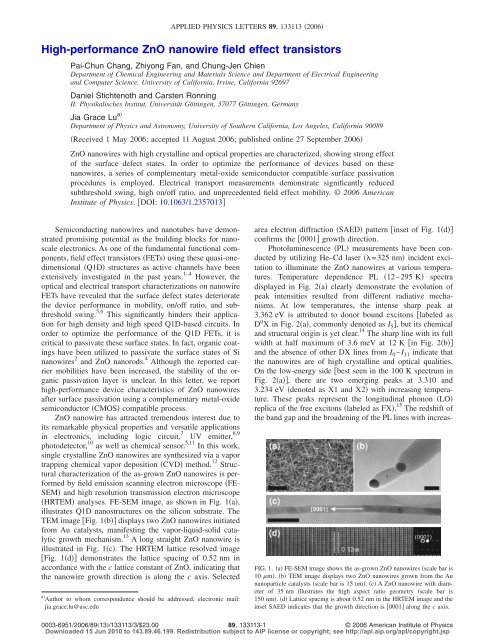
characterization of the as-grown <strong>ZnO</strong> <strong>nanowire</strong>s is performed<br />
by <strong>field</strong> emission scanning electron microscope FE-<br />
SEM and high resolution transmission electron microscope<br />
HRTEM analyses. FE-SEM image, as shown in Fig. 1a,<br />
illustrates Q1D nanostructures on the silicon substrate. The<br />
TEM image Fig. 1b displays two <strong>ZnO</strong> <strong>nanowire</strong>s initiated<br />
from Au catalysts, manifesting the vapor-liquid-solid catalytic<br />
growth mechanism. 13 A long straight <strong>ZnO</strong> <strong>nanowire</strong> is<br />
illustrated in Fig. 1c. The HRTEM lattice resolved image<br />
Fig. 1d demonstrates the lattice spacing of 0.52 nm in<br />
accordance with the c lattice constant of <strong>ZnO</strong>, indicating that<br />
the <strong>nanowire</strong> growth direction is along the c axis. Selected<br />
area electron diffraction SAED pattern inset of Fig. 1d<br />
confirms the 0001 growth direction.<br />
Photoluminescence PL measurements have been conducted<br />
by utilizing He–Cd laser =325 nm incident excitation<br />
to illuminate the <strong>ZnO</strong> <strong>nanowire</strong>s at various temperatures.<br />
Temperature dependence PL 12–295 K spectra<br />
displayed in Fig. 2a clearly demonstrate the evolution of<br />
peak intensities resulted from different radiative mechanisms.<br />
At low temperatures, the intense sharp peak at<br />
3.362 eV is attributed to donor bound excitons labeled as<br />
D 0 X in Fig. 2a, commonly denoted as I 5 , but its chemical<br />
and structural origin is yet clear. 14 The sharp line with its full<br />
width at half maximum of 3.6 meV at 12 K in Fig. 2b<br />
and the absence of other DX lines from I 0 –I 11 indicate that<br />
the <strong>nanowire</strong>s are of high crystalline and optical qualities.<br />
On the low-energy side best seen in the 100 K spectrum in<br />
Fig. 2a, there are two emerging peaks at 3.310 and<br />
3.234 eV denoted as X1 and X2 with increasing temperature.<br />
These peaks represent the longitudinal phonon LO<br />
replica of the free excitons labeled as FX. 15 The redshift of<br />
the band gap and the broadening of the PL lines with increasa<br />
Author to whom correspondence should be addressed; electronic mail:<br />
jia.grace.lu@usc.edu<br />
FIG. 1. a FE-SEM image shows the as-grown <strong>ZnO</strong> <strong>nanowire</strong>s scale bar is<br />
10 m. b TEM image displays two <strong>ZnO</strong> <strong>nanowire</strong>s grown from the Au<br />
nanoparticle catalysts scale bar is 15 nm. c A <strong>ZnO</strong> <strong>nanowire</strong> with diameter<br />
of 35 nm illustrates the high aspect ratio geometry scale bar is<br />
150 nm. d Lattice spacing is about 0.52 nm in the HRTEM image and the<br />
inset SAED indicates that the growth direction is 0001 along the c axis.<br />
0003-6951/2006/8913/133113/3/$23.00<br />
89, 133113-1<br />
© 2006 American Institute of Physics<br />
Downloaded 15 Jun 2010 to 143.89.46.199. Redistribution subject to AIP license or copyright; see http://apl.aip.org/apl/copyright.jsp
133113-2 Chang et al. Appl. Phys. Lett. 89, 133113 2006<br />
FIG. 2. Color online a Set of PL data displays the increasing free exciton<br />
FX luminescence peak and decreasing donor bound exciton D 0 X peak<br />
with rising temperature. LO replica of the FX is observed at X1 and X2. b<br />
The high resolution PL of the band-edge luminescence, taken at 12 K,<br />
shows the sharp D 0 X line as well as the surface bound exciton SX.<br />
ing temperature are results of the interaction of excitons with<br />
optical phonons and increased exciton thermal<br />
ionization. 16,17 The shoulder on the high-energy side labeled<br />
as SX in Fig. 2b originates from the recombination of<br />
surface excitons. This feature scales with the diameter 18 and<br />
reveals the presence of optically active surface states and<br />
confirms the high surface/volume ratio of the as-grown<br />
<strong>nanowire</strong>s.<br />
The as-synthesized <strong>ZnO</strong> <strong>nanowire</strong>s are then fabricated<br />
into FETs. Nanowire suspension is first deposited on a silicon<br />
substrate, which consists of a thermally grown SiO 2<br />
layer 500 nm thick capped on p ++ Si functioning as a back<br />
gate electrode. Photolithography technique is utilized to define<br />
metal leads onto the two ends of individual <strong>ZnO</strong> <strong>nanowire</strong>s<br />
serving as the source and drain electrodes. To achieve<br />
Ohmic contact for attaining high device <strong>performance</strong>, 19,20 the<br />
metal leads composed of 10 nm titanium Ti adhesive layer<br />
and 100 nm gold Au are used. In order to investigate the<br />
uniformity of the <strong>nanowire</strong> channel, multiple electrodes have<br />
been defined on a <strong>nanowire</strong> with equal intervals of 4 m, as<br />
shown in Fig. 3a. The conductances across different channel<br />
segments are found to be proportional to the length Fig.<br />
3b, suggesting that the <strong>nanowire</strong> has high electrical uniformity<br />
and the resistances at the contacts are considerably<br />
lower than that of the channel.<br />
It is well known that metal-oxide surfaces are rich in<br />
defects, predominantly oxygen vacancies which serve as the<br />
binding sites for chemisorption processes. They also contribute<br />
to the scattering and trapping of charge carriers, 21 thus<br />
lowering the carrier mobility. To enhance device <strong>performance</strong>,<br />
it is crucial to passivate the surface states. As a result,<br />
we have employed CMOS compatible processes to passivate<br />
the surfaces of the <strong>nanowire</strong>s with a SiO 2 /Si 3 N 4 bilayer<br />
coating patterned by a polyimide shadow mask. First, the<br />
untreated <strong>nanowire</strong> FETs were placed in a vacuum chamber<br />
10 −6 torr to remove the surface adsorbents such as O 2 and<br />
H 2 O, and then deposited with a layer of SiO 2 100 nm to<br />
prevent subsequent chemical readsorption. Afterwards, a<br />
layer of 50 nm Si 3 N 4 was grown on top of the SiO 2 by<br />
plasma enhanced chemical vapor deposition PECVD under<br />
a temperature of 250 °C to cover the pinholes in the SiO 2<br />
layer, as well as to improve the chemical resistance of the<br />
fabricated devices. Because the PECVD process is conducted<br />
at an elevated temperature, it produces an additional annealing<br />
<strong>effect</strong> that further optimizes the crystallinity of the SiO 2<br />
coating, and it also improves the contact between the <strong>ZnO</strong><br />
<strong>nanowire</strong> and the Ti/Au electrode, yielding a low resistive<br />
Ohmic contact. 19<br />
To distinguish the changes contributed by the surface<br />
passivation, two groups of devices have been prepared: 20<br />
untreated FET devices with <strong>nanowire</strong> channel exposed to the<br />
air and 20 surface treated devices coated with SiO 2 /Si 3 N 4<br />
passivation layers. For a representative sample without any<br />
surface treatment, the source-drain current versus gate voltage<br />
I DS -V GS curves are shown in Fig. 4a. The Q1D carrier<br />
concentration and <strong>field</strong> <strong>effect</strong> mobility are estimated to be<br />
4.010 7 cm −1 and 30 cm 2 /V s using a simple electrostatic<br />
model based on a cylindrical wire with diameter of 80 nm<br />
and length of 4 m. 1,5,22 The subthreshold swing S<br />
logdV GS /dlog I DS , a key parameter for FET scaling, is<br />
about 3 V/decade. 23 On average, the 20 untreated devices<br />
show an on/off ratio of 10 3 at V DS =0.5 V and mobilities<br />
ranging from 20 to 80 cm 2 /V s, which are consistent with<br />
the previously reported values for <strong>ZnO</strong> <strong>nanowire</strong><br />
FETs. 4,5,12,24 In comparison, another 20 devices were coated<br />
with passivation layer and depicted in Fig. 4b. After the<br />
surface treatments, the I DS -V GS curves of a typical sample<br />
measured at different bias voltages V DS are displayed in<br />
Fig. 4c. They exhibit a clear saturation region and a significantly<br />
enhanced on/off ratio on the order of 10 4 even at<br />
V DS =5 mV. For this illustrated example with diameter of<br />
90 nm, a Q1D carrier concentration of 7.510 7 cm −1 and<br />
a much higher mobility of 3118 cm 2 /V s are obtained. In<br />
addition, sub-threshold swing is reduced Fig. 4d, yielding<br />
S150 mV per decade. Statistically, the 20 surface-coated<br />
devices display mobilities ranging from<br />
1200 to 4120 cm 2 /Vs. The origin of the superior FET <strong>performance</strong><br />
is attributed to two factors: 1 passivation of surface<br />
defect states, which act as scattering and trapping centers,<br />
and 2 reduction of surface chemisorption processes at<br />
oxygen vacancy sites. Conclusively, the SiO 2 /Si 3 N 4 passivation<br />
processes have proven to significantly enhance device<br />
<strong>performance</strong> in the subthreshold swing, on/off ratio, and mobility.<br />
On average, the <strong>field</strong> <strong>effect</strong> mobility of <strong>ZnO</strong> <strong>nanowire</strong><br />
FIG. 3. Color online a SEM image<br />
displays the configuration of a <strong>nanowire</strong><br />
device contacted with five electrodes,<br />
labeled as A–E scale bar is<br />
10 m. b I DS -V DS characteristics of<br />
a <strong>ZnO</strong> <strong>nanowire</strong> measured across subsequent<br />
electrode pairs.<br />
Downloaded 15 Jun 2010 to 143.89.46.199. Redistribution subject to AIP license or copyright; see http://apl.aip.org/apl/copyright.jsp
133113-3 Chang et al. Appl. Phys. Lett. 89, 133113 2006<br />
The authors thank the valuable discussion and technical<br />
assistance of Dr. Wen-An Chiou. This project is supported by<br />
NSF Grant No. ECS 0306735 and DFG Grant No. Ro1198/<br />
7-1.<br />
FIG. 4. Color online Transport measurements present a I DS -V GS curves<br />
of a <strong>ZnO</strong> <strong>nanowire</strong> FET without surface treatments showing typical n-type<br />
semiconducting behavior. b Schematic of surface passivated <strong>ZnO</strong> <strong>nanowire</strong><br />
FET with SiO 2 /Si 3 N 4 bilayer covering the <strong>nanowire</strong> channel. c I DS -<br />
V GS of a surface treated <strong>nanowire</strong> FET exhibits significantly enhanced on/off<br />
ratio and transconductance. d Semilog plot demonstrates a tenfold reduction<br />
in the subthreshold swing. At large negative gate voltages, band bending<br />
gives rise to hole conduction.<br />
FETs is dramatically increased by two orders of magnitudes,<br />
with the maximum measured mobility exceeding<br />
4000 cm 2 /V s. It is much higher than the reported mobility<br />
of Si <strong>nanowire</strong> FET Ref. 2 1350 cm 2 /V s and polymer<br />
coated <strong>ZnO</strong> nanorod FET 1200 cm 2 /V s. 4<br />
In summary, we have presented remarkable device characteristics<br />
of <strong>field</strong> <strong>effect</strong> <strong>transistors</strong> based on <strong>ZnO</strong> <strong>nanowire</strong>s<br />
synthesized by catalytic CVD method. The structural and PL<br />
analyses demonstrate the strong <strong>effect</strong> of the surface defect<br />
states. With a series of CMOS compatible surface passivations,<br />
the <strong>nanowire</strong> FETs exhibit improvement in the subthreshold<br />
swing, on/off ratio, and mobility. Since mobility<br />
determines the carrier velocity and thus switching speed,<br />
these <strong>nanowire</strong> FETs demonstrate promising potential as the<br />
building blocks for future applications in high frequency integrated<br />
electronics, such as memory element and logic gate.<br />
1 T. Durkop, S. A. Getty, E. Cobas, and M. S. Fuhrer, Nano Lett. 4, 35<br />
2004.<br />
2 Y. Cui, Z. H. Zhong, D. L. Wang, W. U. Wang, and C. M. Lieber, Nano<br />
Lett. 3, 149 2003.<br />
3 N. Ooike, J. Motohisa, and T. Fukui, J. Cryst. Growth 272, 1752004.<br />
4 W. I. Park, J. S. Kim, G. C. Yi, M. H. Bae, and H. J. Lee, Appl. Phys. Lett.<br />
85, 5052 2004.<br />
5 Z. Y. Fan, D. W. Wang, P. C. Chang, W. Y. Tseng, and J. G. Lu, Appl.<br />
Phys. Lett. 85, 5923 2004.<br />
6 B. Lei, C. Li, D. H. Zhang, Q. F. Zhou, K. K. Shung, and C. W. Zhou,<br />
Appl. Phys. Lett. 84, 4553 2004.<br />
7 W. I. Park, J. S. Kim, G. C. Yi, and H. J. Lee, Adv. Mater. Weinheim,<br />
Ger. 17, 1393 2005.<br />
8 J. C. Johnson, K. P. Knutsen, H. Q. Yan, M. Law, Y. F. Zhang, P. D. Yang,<br />
and R. J. Saykally, Nano Lett. 4, 1972004.<br />
9 W. I. Park and G. C. Yi, Adv. Mater. Weinheim, Ger. 16, 872004.<br />
10 H. Kind, H. Q. Yan, B. Messer, M. Law, and P. D. Yang, Adv. Mater.<br />
Weinheim, Ger. 14, 158 2002.<br />
11 Z. Y. Fan and J. G. Lu, Appl. Phys. Lett. 86, 123510 2005.<br />
12 P. C. Chang, Z. Y. Fan, D. W. Wang, W. Y. Tseng, W. A. Chiou, J. Hong,<br />
and J. G. Lu, Chem. Mater. 16, 5133 2004.<br />
13 R. S. Wagner and W. C. Ellis, Appl. Phys. Lett. 4, 891964.<br />
14 B. K. Meyer, J. Sann, D. M. Hofmann, C. Neumann, and A. Zenner,<br />
Semicond. Sci. Technol. 20, S622005.<br />
15 X. Q. Meng, D. Z. Shen, J. Y. Zhang, D. X. Zhao, L. Dong, Y. M. Lu, Y.<br />
C. Liu, and X. W. Fan, Nanotechnology 16, 6092005.<br />
16 Claus Klingshirn, Semiconductor Optics, 2nd ed. Springer, New York,<br />
2005.<br />
17 T. Makino, C. H. Chia, N. T. Tuan, Y. Segawa, M. Kawasaki, A. Ohtomo,<br />
K. Tamura, and H. Koinuma, Appl. Phys. Lett. 76, 3549 2000.<br />
18 J. Grabowska, A. Meaney, K. K. Nanda, J. P. Mosnier, M. O. Henry, J. R.<br />
Duclere, and E. McGlynn, Phys. Rev. B 71, 115439 2005.<br />
19 K. Ip, G. T. Thaler, H. S. Yang, S. Y. Han, Y. J. Li, D. P. Norton, S. J.<br />
Pearton, S. W. Jang, and F. Ren, J. Cryst. Growth 287, 1492006.<br />
20 S. Y. Kim, H. W. Jang, J. K. Kim, C. M. Jeon, W. I. Park, G. C. Yi, and J.<br />
L. Lee, J. Electron. Mater. 31, 868 2002.<br />
21 G. Eranna, B. C. Joshi, D. P. Runthala, and R. P. Gupta, Crit. Rev. Solid<br />
State Mater. Sci. 29, 111 2004.<br />
22 R. Martel, T. Schmidt, H. R. Shea, T. Hertel, and P. Avouris, Appl. Phys.<br />
Lett. 73, 24471998.<br />
23 A. Javey, H. Kim, M. Brink, Q. Wang, A. Ural, J. Guo, P. McIntyre, P.<br />
McEuen, M. Lundstrom, and H. J. Dai, Nat. Mater. 1, 241 2002.<br />
24 Y. W. Heo, L. C. Tien, Y. Kwon, D. P. Norton, S. J. Pearton, B. S. Kang,<br />
and F. Ren, Appl. Phys. Lett. 85, 2274 2004.<br />
Downloaded 15 Jun 2010 to 143.89.46.199. Redistribution subject to AIP license or copyright; see http://apl.aip.org/apl/copyright.jsp