Chapter 16 FBs-7SG 7/16-segment LED Display Module - SEA
Chapter 16 FBs-7SG 7/16-segment LED Display Module - SEA
Chapter 16 FBs-7SG 7/16-segment LED Display Module - SEA

You also want an ePaper? Increase the reach of your titles
YUMPU automatically turns print PDFs into web optimized ePapers that Google loves.
<strong>Chapter</strong> <strong>16</strong><br />
<strong>FBs</strong>-<strong>7SG</strong> 7/<strong>16</strong>-<strong>segment</strong> <strong>LED</strong> <strong>Display</strong> <strong>Module</strong><br />
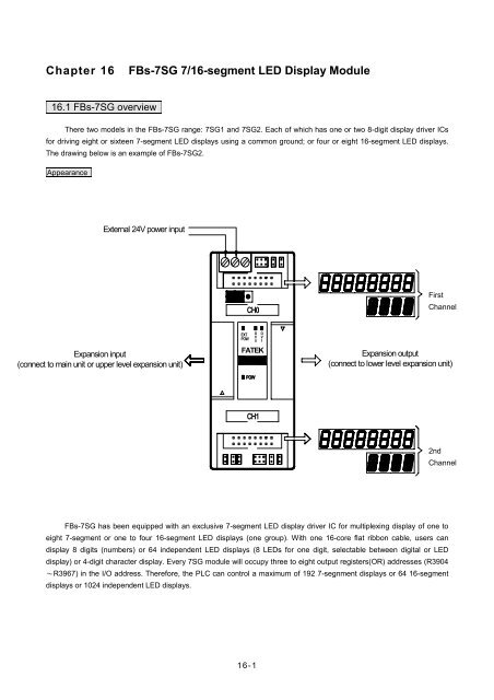
<strong>16</strong>.1 <strong>FBs</strong>-<strong>7SG</strong> overview<br />
There two models in the <strong>FBs</strong>-<strong>7SG</strong> range: <strong>7SG</strong>1 and <strong>7SG</strong>2. Each of which has one or two 8-digit display driver ICs<br />
for driving eight or sixteen 7-<strong>segment</strong> <strong>LED</strong> displays using a common ground; or four or eight <strong>16</strong>-<strong>segment</strong> <strong>LED</strong> displays.<br />
The drawing below is an example of <strong>FBs</strong>-<strong>7SG</strong>2.<br />
Appearance<br />
External 24V power input<br />
CH0<br />
First set<br />
Channel<br />
Expansion input<br />
(connect to main unit or upper level expansion unit)<br />
EXT O O<br />
POW<br />
V V<br />
0 1<br />
FATEK<br />
POW<br />
Expansion output<br />
(connect to lower level expansion unit)<br />
CH1<br />
2nd set<br />
Channel<br />
<strong>FBs</strong>-<strong>7SG</strong> has been equipped with an exclusive 7-<strong>segment</strong> <strong>LED</strong> display driver IC for multiplexing display of one to<br />
eight 7-<strong>segment</strong> or one to four <strong>16</strong>-<strong>segment</strong> <strong>LED</strong> displays (one group). With one <strong>16</strong>-core flat ribbon cable, users can<br />
display 8 digits (numbers) or 64 independent <strong>LED</strong> displays (8 <strong>LED</strong>s for one digit, selectable between digital or <strong>LED</strong><br />
display) or 4-digit character display. Every <strong>7SG</strong> module will occupy three to eight output registers(OR) addresses (R3904<br />
~R3967) in the I/O address. Therefore, the PLC can control a maximum of 192 7-segnment displays or 64 <strong>16</strong>-<strong>segment</strong><br />
displays or 1024 independent <strong>LED</strong> displays.<br />
<strong>16</strong>-1
<strong>16</strong>.2 The procedure of using <strong>FBs</strong>-<strong>7SG</strong> module<br />
Start<br />
Install <strong>FBs</strong>-<strong>7SG</strong> and connect the<br />
24VDC power cable and 7-segnment<br />
<strong>LED</strong> display cable.<br />
• See <strong>FBs</strong>-<strong>7SG</strong> Hardware Wiring, Section <strong>16</strong>.4.1 for details. Refer to<br />
Section <strong>16</strong>.4 for details about the circuit of 7-<strong>segment</strong> <strong>LED</strong> display<br />
Set appropriate driving voltage for each<br />
group according to the number of <strong>LED</strong>s<br />
in each group of the 7-<strong>segment</strong> display<br />
and adjust <strong>LED</strong> to the best display<br />
condition according to the forward<br />
voltage drop of each group and ensure<br />
no over voltage (OV) has occurred.<br />
• See <strong>FBs</strong>-<strong>7SG</strong> Hardware Setup, Section <strong>16</strong>.4.2 for details.<br />
Enter OR to the <strong>FBs</strong>-PLC to light up the<br />
7-<strong>segment</strong> <strong>LED</strong> display or display<br />
characters and numbers by means of<br />
FUN84 (TDSP)<br />
• See FUN84. TDSP Commands, Section <strong>16</strong>.8 for details.<br />
End<br />
<strong>16</strong>.3 <strong>FBs</strong>-<strong>7SG</strong> I/O address<br />
Every <strong>FBs</strong>-<strong>7SG</strong> module will occupy three to eight output registers(OR) addresses (R3904~R3967) in the I/O<br />
address. In general, WinProladder will detect and calculate the actual I/O addresses occupied by the expansion modules<br />
installed on the system after connecting to the PLC. Users may refer to the I/O <strong>Module</strong> Number Configuration provided by<br />
WinProladder in order to find out the exact I/O address of each expansion module to facilitate programming.<br />
<strong>16</strong>.4 <strong>FBs</strong>-<strong>7SG</strong> hardware wiring and setup<br />
<strong>16</strong>.4.1 <strong>FBs</strong>-<strong>7SG</strong> hardware wiring<br />
The hardware wiring diagram of <strong>FBs</strong>-<strong>7SG</strong> is shown above. In addition to the external 24V power, expansion module<br />
input and expansion module output, users will only need to connect the output to a 7-/<strong>16</strong>-<strong>segment</strong> <strong>LED</strong> display board with<br />
an <strong>16</strong>-core FRC flat ribbon cable.<br />
<strong>16</strong>-2
<strong>16</strong>.4.2 <strong>FBs</strong>-<strong>7SG</strong> hardware setup<br />
The drawing below presents the output driver circuit of the internal display IC on <strong>FBs</strong>-<strong>7SG</strong>. General users will not<br />
need to calculate the voltage drop of <strong>LED</strong>s. They will only need to adjust the voltage according to the jumper table below<br />
in order to prevent over voltage.<br />
40mA<br />
Driving power source<br />
VIN<br />
Fixed current for<br />
displaying IC<br />
7-<strong>segment</strong> <strong>LED</strong><br />
displayer<br />
VIC=VIN - V<strong>LED</strong> - 0.8V<br />
PD=40mA VIC ≦ 0.8W<br />
V<strong>LED</strong>=(1.7 2.8V) Numbers of cascade<br />
connected amp sect <strong>LED</strong><br />
Multiplexing scan<br />
VMUX<br />
0.8V(Fixed)<br />
The power consumption will completely depend on the amount of voltage drop V IC (P D = 40mA × V IC) connected to it<br />
because the IC current source is fixed at 40mA. As shown in the above diagram, V IC = V IN − V <strong>LED</strong> − 0.8V, i.e. V IC is<br />
affected by the driving current voltage V IN and the forward voltage drop of the 7-<strong>segment</strong> display V <strong>LED</strong>, because the safety<br />
power consumption of display IC at the severest ambient temperature condition must be controlled at or under 0.8W; i.e.<br />
V IC must be smaller than 2V. If the V IC is too low, the brightness of the <strong>LED</strong> will be reduced; if it is too high, it will result in<br />
incorrect display (<strong>LED</strong>s that are not supposed to be lighted up will be lighted up) or display IC damage.<br />
The forward voltage drop of <strong>LED</strong> is generally between 1.7V and 2.8V. Depending on the size of ordinary 7-<strong>segment</strong><br />
or <strong>16</strong>-<strong>segment</strong> <strong>LED</strong> displays, each <strong>segment</strong> (e.g. a-g) consists of one to five <strong>LED</strong>s connected in series. While the range<br />
of forward voltage drop among <strong>segment</strong>s will be from 1.7V to 14V, it will be impossible to drive different <strong>LED</strong> displays with<br />
a single voltage. In order to drive the majority 7-<strong>segment</strong> <strong>LED</strong> displays, <strong>FBs</strong>-<strong>7SG</strong> comes with four driving voltage options<br />
at 5V (low-voltage), 7.5V, 10V and 12.5V (high voltage for the last three options) and a fine tuning function at 0.6V-1.8V<br />
by means of the diodes and jumpers incorporated to them. In practice, the power supply can drive <strong>LED</strong>s of different<br />
forward voltages and prevent display IC from blowing by limiting V IC within 2V. The diagrams below show the high/low<br />
voltage setup (common) of <strong>LED</strong> on <strong>FBs</strong>-<strong>7SG</strong>, the high/low voltage driving options of displays and the jumper setting of<br />
forward voltage drop fine tuning, and its exaction location (as seen after opening the top cover of <strong>FBs</strong>-<strong>7SG</strong>).<br />
In this section, we will show you how to obtain the optimal display of 7-/<strong>16</strong>-<strong>segment</strong> <strong>LED</strong> displays without blowing or<br />
shorten the life of the display IC by means of driving voltage (V IN) setup, high/low voltage selection and forward voltage<br />
fine tuning.<br />
<strong>16</strong>-3
<strong>FBs</strong>-<strong>7SG</strong> jumper location<br />
HV<br />
LV<br />
JP5 JP6 .6V<br />
JP7<br />
1V2<br />
JP1<br />
D<br />
JP2<br />
JP10<br />
1V2<br />
T JP9 .6V<br />
JP3<br />
JP8<br />
HV<br />
LV<br />
Jumper 插 Layout 梢 位 置 (open 圖 ( 打 top 開 cover) 上 蓋 )<br />
Jumper 插 Layout 梢 位 置 (back ( 背 面 of ) module)<br />
The jumper settings below are referred to <strong>FBs</strong>-<strong>7SG</strong>2, because they have covered those in <strong>FBs</strong>-<strong>7SG</strong>1.<br />
Attribute Jumper Function<br />
Common<br />
CH0<br />
JP2<br />
JP3<br />
JP1<br />
JP5<br />
JP6<br />
Decode (D closed)/Non-decode (D<br />
open) setting<br />
O.V. Test (T) or Normal (No Jumper)<br />
setting<br />
High Voltage (HV) selection (back of<br />
module)<br />
High (HV)/Low (LV) voltage selection<br />
0.6V(0.6V) voltage drop fine tuning<br />
<strong>FBs</strong>-<strong>7SG</strong>1<br />
<strong>FBs</strong>-<strong>7SG</strong>2<br />
JP7<br />
1.2V(1V2) voltage drop fine tuning<br />
JP8<br />
High (HV)/Low (LV) voltage selection<br />
CH1<br />
JP9<br />
0.6V(0.6V) voltage drop fine tuning<br />
JP10<br />
1.2V(1V2) voltage drop fine tuning<br />
<strong>16</strong>-4
JP5/JP8 JP1 JP7/JP10 JP6/JP9<br />
LV<br />
HV<br />
Inactive<br />
7.5V<br />
10V<br />
12.5V<br />
<strong>LED</strong> Driving<br />
Voltage<br />
Open Open 2.4V<br />
Open Short 3V<br />
Short Open 3.6V<br />
Short Short 4.2V<br />
Open Open 4.9V<br />
Open Short 5.5V<br />
Short Open 6.1V<br />
Short Short 6.7V<br />
Open Open 7.4V<br />
Open Short 8V<br />
Short Open 8.6V<br />
Short Short 9.2V<br />
Open Open 9.9V<br />
Open Short 10.5V<br />
Short Open 11.1V<br />
Short Short 11.7V<br />
Short JP5/JP8 with a jumper<br />
horizontally; place the jumper head onto<br />
the JP5/JP8.<br />
JP1 is located at the back of the module.<br />
Turn module over for setup.<br />
Short only one of the three options<br />
above. JP1 is effective only when HV is<br />
selected from JP5. When LV is selected<br />
from JP5, JP1 will be ineffective.<br />
When BOOST is short, the driving<br />
voltage will be boosted by 5% to<br />
compensate circuit voltage drop. JP5 to<br />
JP7 are effective on CH0 and JP8-JP10<br />
on CH1.<br />
<strong>16</strong>-5
<strong>16</strong>.4.3 <strong>LED</strong> driving voltage setup and over-voltage (OV) inspection<br />
Users must select the correct driving voltage according to the voltage requirements of <strong>LED</strong>s of different sizes before<br />
applying the module. If the voltage is too low, the brightness of <strong>LED</strong>s will be reduced. If the voltage is too high, the<br />
brightness of <strong>LED</strong>s will be uneven. More importantly, the <strong>LED</strong> driver IC will be blown due to over-voltage (O.V.).<br />
Therefore, it is necessary to make sure that the CE intermittent voltage (VIC) of the driver IC is below 2V to prevent an<br />
O.V. of the driver IC. Yet, it is difficult for users to measure the VIC of driver IC in multiplexing. Therefore, <strong>FBs</strong>-<strong>7SG</strong> is<br />
equipped with an O.V. <strong>LED</strong> indicator to facilitate users to check if an OV occurs. The O.V. indicator is located next to the<br />
output socket on the panel labeled with O.V.<br />
The result of the O.V. indicator is meaningful only when all <strong>segment</strong>s (a total of 64, including the decimal point) are<br />
lighted up. If the O.V. indicator is out in this situation, it means there is no O.V. If the indicator is on, it means there is an<br />
O.V. (the indicator may blink or is on constantly if not all <strong>segment</strong>s are lighted up, in this case, it is meaningless). If you<br />
want to perform a full <strong>segment</strong> test, set the TEST Jumper (JP3) to “T” (only when the PLC is OFF) on the lower left part of<br />
<strong>7SG</strong> or use the convenient command (FUN84:TDSP) on <strong>7SG</strong> by setting All Input-ON to “1” (PLC is in “RUN” mode) to<br />
light up all <strong>segment</strong>s for an O.V. test.<br />
The following examples show the <strong>LED</strong> of <strong>FBs</strong>-<strong>7SG</strong> module driving voltage setup and O.V. test procedures.<br />
1. Set JP3 to “T” or All Input-ON of FUN84:TDSP to “1”.<br />
2. Start with LV and then adjust driving voltage to the required brightness or the O.V. indicator is on according to the<br />
jumper setting as shown in the table above. When the O.V. indicator is on, reduce voltage until the O.V. indicator is<br />
off. Please be noted that if the brightness is at its maximum level but it cannot meet the requirements, replace <strong>LED</strong>s<br />
with higher efficiency.<br />
3. Set JP3 back to ‘N” (normal position) or All Input-ON of FUN84:TDSP to “0”.<br />
Caution<br />
The 7-<strong>segment</strong> <strong>LED</strong> display of <strong>FBs</strong>-<strong>7SG</strong> is driven by the driver IC with a rated current ≒40mA. The<br />
power consumption depends on the VIC of CE because the maximum power limit is only 0.7W/25°C, do<br />
not use module in O.V. condition to prevent the driver IC from blowing.<br />
<strong>16</strong>-6
<strong>16</strong>.5 7-<strong>segment</strong> <strong>LED</strong> display and individual <strong>LED</strong> display circuits<br />
(D0) a<br />
(D1) b<br />
(D2) c<br />
(D3) d<br />
(D4) e<br />
(D5) f<br />
(D6) g<br />
(D7)<br />
Independent<br />
<strong>LED</strong><br />
displaying<br />
of<br />
non-decoding<br />
mode<br />
7-<strong>segment</strong><br />
displayer or<br />
Independent <strong>LED</strong><br />
g f e d c b a g f d<br />
e c b a g f c<br />
e d b a g f e d c b a<br />
6463626<strong>16</strong>0595857<br />
5655545352 515049<br />
<strong>16</strong>151413121110 9<br />
8<br />
7<br />
6<br />
5<br />
4<br />
3<br />
2 1<br />
Digit<br />
displaying<br />
of mode<br />
decoding<br />
8(Most significant)<br />
7<br />
6<br />
5<br />
4<br />
3<br />
2<br />
1(Least significant)<br />
15<br />
1<br />
<strong>16</strong><br />
2<br />
The above diagram indicates the correct wiring (common ground) of the 7-<strong>segment</strong> <strong>LED</strong> display or independent<br />
<strong>LED</strong> display of <strong>FBs</strong>-<strong>7SG</strong>. Users may make their own display according to this circuit and layout and connect the display to<br />
any output socket on <strong>FBs</strong>-<strong>7SG</strong> with a <strong>16</strong>-pin flat ribbon cable. We offer <strong>LED</strong> display boards and products in six different<br />
dimensions to meet the demands of users. The table below shows the range of our <strong>LED</strong> display boards and products.<br />
<strong>16</strong>-7
Model<br />
Specification<br />
DBAN.8 (DBAN.8<strong>LED</strong>R) 0.8” x 4 <strong>16</strong>-<strong>segment</strong> <strong>LED</strong> display board (with red <strong>LED</strong>s onboard)<br />
DBAN2.3 (DBAN2.3<strong>LED</strong>R) 2.3” x 4 <strong>16</strong>-<strong>segment</strong> <strong>LED</strong> display board (with red <strong>LED</strong>s onboard)<br />
DB.56 (DB.56<strong>LED</strong>R) 0.56” x 8 7-<strong>segment</strong> <strong>LED</strong> display board (with red <strong>LED</strong>s onboard)<br />
DB.8 (DB.8<strong>LED</strong>R) 0.8” x 8 7-<strong>segment</strong> <strong>LED</strong> display board (with red <strong>LED</strong>s onboard)<br />
DB2.3 (DB2.3<strong>LED</strong>R) 2.3” x 8 7-<strong>segment</strong> <strong>LED</strong> display board (with red <strong>LED</strong>s onboard)<br />
DB4.0 (DB4.0<strong>LED</strong>R) 4.0” x 4 7-<strong>segment</strong> <strong>LED</strong> display board (with red <strong>LED</strong>s onboard)<br />
※ Models inside parentheses are products equipped with <strong>LED</strong> display and ribbon cable socket.<br />
Recommended pin settings<br />
Model<br />
HV/LV<br />
(JP5/JP8)<br />
JP1 JP7/JP10 JP6/JP9 Driving Voltage<br />
DBAN.8 LV Open Short 3V<br />
DBAN2.3 HV 10V Open Open 7.4V<br />
DB.56 LV Open Open 2.4V<br />
DB.8 LV Short Open 3.6V<br />
DB2.3 HV 10V Short Short 9.2V<br />
DB4.0 HV 10V Short Open 8.6V<br />
Users can adjust the pin settings tabulated above table on any FATEK standard products. If higher brightness is<br />
desired, users can fine-tune the driving voltage according to the jumper settings as shown above. Users must avoid over<br />
voltage (O.V.) of output (O.V. indicator will light up) in order not to blow the <strong>7SG</strong> module.<br />
Connector pin layout<br />
Pin Signal Pin Signal<br />
1 DIG0 2 DIG1<br />
3 DIG2 4 DIG3<br />
5 DIG4 6 DIG5<br />
7 DIG6 8 DIG7<br />
9 a/D0 10 b/D1<br />
11 c/D2 12 d/D3<br />
13 e/D4 14 f/D5<br />
15 g/D6 <strong>16</strong> p/D7<br />
There are two display output connectors on <strong>7SG</strong>2, each can support 64 <strong>segment</strong>s of <strong>LED</strong> display. When all<br />
<strong>segment</strong>s are on, 8 <strong>segment</strong>s will be scanned at a time for a total of 8 times.<br />
DIG0-DIG7 as tabulated above refer to low active output signals (Sink or NPN output), only one signal will be active<br />
(multiplexing) at the same time to select a group of <strong>LED</strong>s (8 <strong>segment</strong>s). a/D0-p/D7 are source output signals (PNP)<br />
controlling the display of corresponding <strong>segment</strong>s.<br />
<strong>16</strong>-8
<strong>16</strong>.6 Decode display and non-decode display<br />
○1 Non-decode display: (All <strong>segment</strong>s are dimmed, controlled by user-defined applications independently)<br />
A total of 8 ORs are equipped on <strong>FBs</strong>-<strong>7SG</strong>2 to control the display of 128 <strong>segment</strong>s. Each <strong>segment</strong> is controlled by a<br />
corresponding bit. When the bit value is 1, the corresponding <strong>segment</strong> will light up. The correlations of each <strong>segment</strong> and<br />
OR is tabulated below. OR is the first output register that occupied by the module. Each OR will output signals twice, i.e. 1<br />
bit of data (8 <strong>segment</strong>s) each time. These data will be transferred to the corresponding outputs p/D7-a/D0.<br />
OR D15~D8 D7~D0<br />
OR+0 SEG15~SEG8 SEG7~SEG0<br />
CH0<br />
OR+1 SEG31~SEG24 SEG23~SEG<strong>16</strong><br />
OR+2 SEG47~SEG40 SEG39~SEG32<br />
OR+3 SEG63~SEG56 SEG63~SEG48<br />
OR+4 SEG15~SEG8 SEG7~SEG0<br />
CH1<br />
OR+5 SEG31~SEG24 SEG23~SEG<strong>16</strong><br />
OR+6 SEG47~SEG40 SEG39~SEG32<br />
OR+7 SEG63~SEG56 SEG63~SEG48<br />
7-<strong>segment</strong> <strong>LED</strong> correspondence<br />
D6<br />
a<br />
D1 f<br />
b D5<br />
D0<br />
g<br />
D2 e<br />
c D4<br />
The digit on the farthest right of the display board (8 digits, max.)<br />
corresponds to outputs SEG0-SEG7; the next digit to the left corresponds to<br />
outputs SEG8-SEG15; the digit on the farthest left of the display board<br />
corresponds to outputs SEG63-SEG56. Each <strong>7SG</strong>2 can drive sixteen<br />
7-<strong>segment</strong> <strong>LED</strong> displays.<br />
d<br />
D3<br />
P<br />
D7<br />
<strong>16</strong>-<strong>segment</strong> <strong>LED</strong> correspondence<br />
Segments D0-D15 of the digit on the farthest right of the display board (4<br />
digits, max.) correspond to outputs SEG0-SEG15 on <strong>7SG</strong>2; the next digit to<br />
the left corresponds to outputs SEG<strong>16</strong>-SEG31; the digit on the farthest left of<br />
the display board corresponds to outputs SEG63-SEG48. Each <strong>7SG</strong>2 can<br />
drive 8 <strong>16</strong>-<strong>segment</strong> <strong>LED</strong> displays.<br />
<strong>16</strong>-9
○2 Decode <strong>Display</strong> : <strong>Display</strong> data on the corresponding <strong>segment</strong>s with default coding<br />
In this mode, a total of 5 output registers(OR) are equipped on <strong>FBs</strong>-<strong>7SG</strong>2 to control the display of <strong>16</strong> digits of<br />
7-<strong>segment</strong> <strong>LED</strong>s. Each digit is controlled by 4 bits. The decimal point of an 8-digit number is controlled by the first output<br />
register. Each point is controlled by the corresponding bit. The correlations among the digits, decimal point and ORs are<br />
tabulated below. OR is the first output register that occupied by the module.<br />
Attribute OR D15~D12 D11~D8 D7~D4 D3~D0<br />
Common OR+0 P15~P8 P7~P0<br />
OR+1 DIG3 DIG2 DIG1 DIG0<br />
CH0<br />
OR+2 DIG7 DIG6 DIG5 DIG4<br />
OR+3 DIG3 DIG2 DIG1 DIG0<br />
CH1<br />
OR+4 DIG7 DIG6 DIG5 DIG4<br />
1_st 8-digit<br />
2_nd 8-digit<br />
OR0 controls the display of decimal point. When the value is “1”, the corresponding decimal point will light up.<br />
OR1-OR4 control the display of <strong>16</strong>-digit numbers. Each digit will be controlled by four corresponding bits. A total of <strong>16</strong><br />
changes correspond to the following displays.<br />
4-bit digital 7-<strong>segment</strong> <strong>LED</strong> decode and non-decode number displays<br />
Segment DIM (0)<br />
Nibble Value 7-<strong>segment</strong> <strong>LED</strong><br />
ON (1)<br />
display structure<br />
Hexadecimal Binary<br />
a b c d e f g<br />
0 0000 1 1 1 1 1 1 0<br />
1 0001 0 1 1 0 0 0 0<br />
2 0010 1 1 0 1 1 0 1<br />
3 0011 1 1 1 1 0 0 1<br />
Number<br />
4 0100 0 1 1 0 0 1 1<br />
a<br />
5 0101 1 0 1 1 0 1 1<br />
f<br />
b<br />
6 0110 1 0 1 1 1 1 1<br />
7 0111 g 1 1 1 0 0 1 0<br />
8 1000 1 1 1 1 1 1 1<br />
e<br />
9 1001 1 1 1 1 0 1 1<br />
d<br />
A 1010 0 0 0 0 0 0 1<br />
B 1011 1 0 0 1 1 1 1<br />
C 1100 0 1 1 0 1 1 1<br />
D 1101 0 0 0 1 1 0 1<br />
E 1110 0 0 0 1 1 1 1<br />
F 1111<br />
0 0 0 0 0 0 0<br />
c<br />
P<br />
<strong>16</strong>-10
ASCII Code and <strong>16</strong>-<strong>segment</strong> number display cross-reference table<br />
MSB<br />
LSB<br />
x000 x001 x010 x011 x100 x101<br />
x110<br />
x111<br />
0000<br />
0001<br />
0010<br />
0011<br />
0100<br />
0101<br />
0110<br />
0111<br />
1000<br />
1001<br />
1010<br />
1011<br />
1100<br />
1101<br />
1110<br />
1111<br />
<strong>16</strong>-11
<strong>16</strong>.7 <strong>FBs</strong>-<strong>7SG</strong> input power requirements and consumption<br />
<strong>FBs</strong>-<strong>7SG</strong> is equipped with a DC24V isolated power supply to convert an external 24V power input into power supply<br />
for use by the internal circuit and 7-<strong>segment</strong> <strong>LED</strong> display on <strong>FBs</strong>-<strong>7SG</strong>. The tolerance of input is DC24V±20%.<br />
<strong>FBs</strong>-<strong>7SG</strong> consumes 2Wmax when idled. The consumption increases according to the number of 7-<strong>segment</strong>s lighted<br />
up. The <strong>segment</strong> driving current of every display IC on <strong>FBs</strong>-<strong>7SG</strong> is 40mA. The driving current for displaying one digit<br />
using 8 <strong>segment</strong>s consumes 320mA, and the maximum power consumption of a group is obtained as formulated below:<br />
Pd = 320mA × VIN (<strong>LED</strong> driving voltage) ÷ 0.8 (power efficiency) W<br />
Total consumption = 2 + Pd × n(W)<br />
For example, the total power consumption of <strong>FBs</strong>-<strong>7SG</strong>2 (output from both groups) at maximum power (VIN = 12.5V,<br />
all 8 <strong>segment</strong>s are on):<br />
2W +(320mA × 12.5V ÷8 )= 7W<br />
<strong>16</strong>.8 Controlling display contents with OR on <strong>FBs</strong>-<strong>7SG</strong><br />
There are two ways to light up an <strong>LED</strong> with <strong>FBs</strong>-<strong>7SG</strong>. In this section, we will introduce the method of how to light up<br />
a 7-<strong>segment</strong> number display by programming the OR output. In the next section, we will continue with displaying special<br />
symbols with FUN84. If displaying numbers with OR controls in decode mode, digits in front of a number will be displayed<br />
as 0.<br />
If expansion modules are connected to the <strong>FBs</strong> PLC, these modules and the I/O address they occupied (see<br />
<strong>Chapter</strong> 12, WinProladder User’s Manual for details) will be displayed on the screen when WinProladder is connected to<br />
the PLC. If a <strong>FBs</strong>-<strong>7SG</strong>2 is connected to the <strong>FBs</strong> PLC, users will find in the project window that the system has<br />
automatically assigned the output address to <strong>FBs</strong>-<strong>7SG</strong>2 when WinProladder is connected to the PLC.<br />
Program example 1 (Decode <strong>Display</strong> Mode)<br />
Control of 8-digit 7-<strong>segment</strong> display with <strong>FBs</strong>-<strong>7SG</strong>1, with decimal point on. In this case, the <strong>FBs</strong>-<strong>7SG</strong>1 must be set<br />
to Decode Mode.<br />
M0<br />
EN<br />
08.MOV<br />
S : 00FFH<br />
D : R3904<br />
08.MOV<br />
EN S :<br />
D :<br />
5678H<br />
R3905<br />
08.MOV<br />
EN S :<br />
D :<br />
1234H<br />
R3906<br />
<strong>16</strong>-12
Description :<br />
When M0=1, move the value to be output to the OR. As described above, OR+0 (R3904 in the example) controls<br />
the display of decimal point in decode mode; OR+1 (R3905 in the example) controls the display of the lower section of the<br />
four digits and OR+2 (R3906 in the example) the upper section of the four digits. The results are:<br />
OR<br />
R3904<br />
R3905<br />
R3906<br />
Contents<br />
00FFH<br />
5678H<br />
1234H<br />
7-<strong>segment</strong> display contents : 1.2.3.4.5.6.7.8.<br />
Program example 2 (Non-decode <strong>Display</strong> Mode)<br />
<strong>Display</strong> numbers on the 8-digit 7-<strong>segment</strong> display with <strong>FBs</strong>-<strong>7SG</strong>1, with decimal point on. In this case, the <strong>FBs</strong>-<strong>7SG</strong>1<br />
must be set to Non-decode Mode.<br />
M0<br />
EN<br />
08.MOV<br />
S : EDB0H<br />
D : R3904<br />
08.MOV<br />
EN S :<br />
D :<br />
B3F9H<br />
R3905<br />
EN<br />
EN<br />
08.MOV<br />
S : DFDBH<br />
D : R3906<br />
08.MOV<br />
S : CFBDH<br />
D : R3907<br />
Description :<br />
When M0=1, move the value to be output to the OR. As described above, OR+0 (R3904 in the example) controls<br />
the display of the first two digits, OR+1 (R3905 in the example) the third and fourth digits, OR+2 (R3906 in the example)<br />
the fifth and sixth digits, and OR+3(R3907 in the example) the last two digits. The results are:<br />
OR<br />
R3904<br />
R3905<br />
R3906<br />
R3907<br />
Contents<br />
EDB0H<br />
B3F9H<br />
DFDBH<br />
CFBDH<br />
7-<strong>segment</strong> display contents : E.d.6.5.4.3.2.1.<br />
<strong>16</strong>.9 <strong>FBs</strong>-<strong>7SG</strong> output commands FUN84: TDSP<br />
The TDSP commands are described in the next page.<br />
<strong>16</strong>-13
TDSP<br />
FUN84<br />
TDSP<br />
<strong>FBs</strong>-<strong>7SG</strong> <strong>Display</strong> <strong>Module</strong> Convenient Commands<br />
7/<strong>16</strong>-<strong>segment</strong> display character and number display conversion<br />
FUN84<br />
TDSP<br />
Execution control<br />
All OFF Input control<br />
All ON Input control<br />
EN<br />
OFF<br />
ON<br />
Ladder symbol<br />
84.TDSP<br />
Md :<br />
S :<br />
N S :<br />
N L :<br />
D :<br />
N d :<br />
Md : Operation Mode, 0~3<br />
S : Starting address of being converted characters<br />
Ns : Start of source character, 0~63<br />
Nl : Length of character, 1~64<br />
D : Starting address to store the converted pattern<br />
Nd : Start pointer while storing<br />
S operand can be combined with V、Z、P0~P9<br />
index registers for indirect addressing<br />
Oper<br />
-and<br />
Range<br />
HR OR ROR DR K Index<br />
R0<br />
∣<br />
R3839<br />
R3904<br />
∣<br />
R3967<br />
R5000<br />
∣<br />
R8071<br />
D0<br />
∣<br />
D3999<br />
Positive<br />
integer<br />
<strong>16</strong>/32-bit<br />
Md 0 ~ 3<br />
V、 Z 、<br />
P0~ P9<br />
S ○ ○ ○ ○ ○<br />
Ns ○ ○ ○ ○ 0 ~ 63<br />
Nl ○ ○ ○ ○ 1 ~ 64<br />
D ○ ○ ○* ○<br />
Nd ○ ○ ○* ○ 0 ~ 63<br />
●<br />
This convenient instruction is used to generate the corresponding display pattern for <strong>FBs</strong> series 7-<strong>segment</strong> or<br />
<strong>16</strong>-<strong>segment</strong> display pannel under the control of <strong>FBs</strong>-<strong>7SG</strong>1 or <strong>FBs</strong>-<strong>7SG</strong>2 modules.<br />
When execution control "EN"=1, input "OFF"=0, and input "ON"= 0, this instruction will perform the display<br />
pattern conversion, where S is the starting address storing the being converted characters, Ns is the pointer<br />
to locate the starting character, Nl tells the length of being converted characters, and D is the starting address<br />
to store the converted result, Nd is the pointer to locate the start of storing.<br />
There are 4 kinds of operation mode as below:<br />
Md=0, display pattern conversion for <strong>16</strong>-<strong>segment</strong> display; the source character is the<br />
8-bit ASCII Code, the converted result is the <strong>16</strong>-bit display pattern. By the<br />
control of M1990, it determines the display direction, where<br />
M1990=0, right to left display ; M1990=1, left to right display<br />
Md=1, Without leading zero display conversion for <strong>16</strong>-<strong>segment</strong> display; the source<br />
character is the 8-bit ASCII Code, the converted result is the <strong>16</strong>-bit display<br />
pattern without leading zero.<br />
Md=2, Non-decoded display pattern conversion for 7-<strong>segment</strong> display; the source<br />
character is the 4-bit nibble code, the converted result is the 8-bit display pattern.<br />
Md=3, Without leading zero display conversion for 7-<strong>segment</strong> decoded display; the<br />
source character is the 4-bit nibble code, the converted result is the 4-bit display<br />
pattern without leading zero.<br />
Byte 0 or Nibble 0 of S is the 1 st displaying character, Byte 1 or Nibble 1 of S is the 2 nd displaying character,…<br />
Ns operand is the pointer to tell where the displaying character starts<br />
Nl operand is the character quantity for conversion<br />
<strong>16</strong>-14
TDSP<br />
FUN84<br />
TDSP<br />
<strong>FBs</strong>-<strong>7SG</strong> <strong>Display</strong> <strong>Module</strong> Convenient Commands<br />
7/<strong>16</strong>-<strong>segment</strong> display character and number display conversion<br />
FUN84<br />
TDSP<br />
D oerand is the starting address to store the converted display pattern; while Md=0 or 1, one source<br />
character of 8-bit ASCII code needs one <strong>16</strong>-bit location to store the result; while Md=2, one source character<br />
of 4-bit nibble code needs one 8-bit location to store it; while Md=3, one source character of 4-bit nibble code<br />
needs one 4-bit location to store it.<br />
Nd operand is the pointer to tell where is the start to store the converted pattern.<br />
●<br />
When inputs "OFF"=1, "ON"=0, and "EN"=0/1, the D operand will be filled with the all OFF pattern according<br />
to the operation mode, the Nd pointer, and the quantity of Nl.<br />
●<br />
When inputs "ON"=1, "OFF"=0/1, and "EN"=0/1, the D operand will be filled with the all ON pattern according<br />
to the operation mode, the Nd pointer, and the quantity of Nl.<br />
● Data will be converted differently based on the selected mode. The description below is based on Example 2.<br />
In Example 2, MD=1; S=R0; Ns=0; Nl=8; D=R3904; and Nd=8. Data conversion is presented below.<br />
Example1<br />
8-character of text display by using the <strong>FBs</strong>-<strong>7SG</strong>2 display module and <strong>16</strong>-Segment display pannels; for<br />
this application, the <strong>FBs</strong>-<strong>7SG</strong>2 module must be set to work at the non-decoded operation mode.<br />
The WinProladder supports the "ASCII Table" editing for easy and convenient text message display; we<br />
can create one ASCII Table with the content ' WELCOME ' for testing, and we assign R5000 is the table<br />
starting address, then R5000~R5007 will have the follwoing contents :<br />
<strong>16</strong>-15
TDSP<br />
FUN84<br />
TDSP<br />
<strong>FBs</strong>-<strong>7SG</strong> <strong>Display</strong> <strong>Module</strong> Convenient Commands<br />
7/<strong>16</strong>-<strong>segment</strong> display character and number display conversion<br />
FUN84<br />
TDSP<br />
R5000=2027H (20H= ; 27H=')<br />
R5001=4557H (45H=E; 57H=W)<br />
R5002=434CH (43H=C; 4CH=L)<br />
R5003=4D4FH (4DH=M; 4FH=O)<br />
R5004=2045H (20H= ; 45H=E)<br />
R5005=2C27H (2CH=,; 27H=')<br />
R5006=4E45H (4EH=N; 45H=E)<br />
R5007=0044H (00H= ; 44H=D)<br />
S500<br />
M1990<br />
M100<br />
M101<br />
M102<br />
EN<br />
OFF<br />
ON<br />
84.TDSP<br />
MD: 0<br />
S :<br />
NS:<br />
R5000<br />
2<br />
Nl : 8<br />
D : R3904<br />
Nd: 0<br />
Description: When M100=1, M101=0 and M102=0, the FUN84 will perform the display pattern conversion, where<br />
the source (S) begins from the R5000, the start pointer (Ns) is pointed to byte 2, and the quantity<br />
(Nl) is 8, it means the contens of R5001~R5004 are the displaying characters; the registers<br />
R3904~R3911 will store the converted pattern for text message displaying (D operand begins from<br />
R3904, Nd operand is pointed to word 0, Nl operand is 8 for quantity)<br />
While M1990=1, the <strong>16</strong>-<strong>segment</strong> pannel will display "WELCOME " ;<br />
While M1990=0, the <strong>16</strong>-<strong>segment</strong> pannel will display " EMOCLEW".<br />
When M101=1, M102=0, the registers R3904~R3911 will be filled with the all OFF pattern for<br />
displaying.<br />
When M102=1, the registers R3904~R3911 will be filled with the all ON pattern for displaying.<br />
Example2<br />
8-character of display without the leading zeor through the second <strong>FBs</strong>-<strong>7SG</strong>2 display module and<br />
<strong>16</strong>-Segment display pannels; for this application, the <strong>FBs</strong>-<strong>7SG</strong>2 module must be set to work at the non-decoded<br />
operation mode.<br />
M110<br />
EN<br />
OFF<br />
ON<br />
84.TDSP<br />
MD: 1<br />
S :<br />
NS:<br />
R0<br />
0<br />
Nl : 8<br />
D : R3904<br />
Nd: 8<br />
<strong>16</strong>-<strong>16</strong>
TDSP<br />
FUN84<br />
TDSP<br />
<strong>FBs</strong>-<strong>7SG</strong> <strong>Display</strong> <strong>Module</strong> Convenient Commands<br />
7/<strong>16</strong>-<strong>segment</strong> display character and number display conversion<br />
FUN84<br />
TDSP<br />
Description<br />
When M110=1, the FUN84 will perform the display pattern conversion, where the source (S) begins from<br />
the R0, the start pointer (Ns) is pointed to byte 0, and the quantity (Nl) is 8, it means the contens of R0~<br />
R3 are the displaying characters; the registers R3912~R3919 will store the converted pattern for<br />
message displaying (D operand begins from R3904, Nd operand is pointed to word 8, Nl operand is 8 for<br />
quantity).<br />
(1) R0=0008H<br />
R1=0506H<br />
R2=0304H<br />
R3=0102H<br />
<strong>Display</strong> on the <strong>16</strong>-<strong>segment</strong> display : "12345608"<br />
(2) R0=0708H<br />
R1=0506H<br />
R2=0000H<br />
R3=0000H<br />
<strong>Display</strong> on the <strong>16</strong>-<strong>segment</strong> display : " 5678"<br />
(3) R0=3738H<br />
R1=3536H<br />
R2=3334H<br />
R3=3132H<br />
<strong>Display</strong> on the <strong>16</strong>-<strong>segment</strong> display : "12345678"<br />
(4) R0=3038H<br />
R1=3536H<br />
R2=3334H<br />
R3=3030H<br />
<strong>Display</strong> on the <strong>16</strong>-<strong>segment</strong> display : " 345608"<br />
※ The I/O address of <strong>FBs</strong>-<strong>7SG</strong>2 in Example 2 must be at R3912~R3919 to ensure the correct display of the<br />
message/number (length=8); i.e. other digital or analog output modules may be connected in front of <strong>FBs</strong>-<strong>7SG</strong>2.<br />
Example3<br />
4-digit of numeric display and 32-point of external independent <strong>LED</strong>'s display through the control of<br />
<strong>FBs</strong>-<strong>7SG</strong>1 display module and 4-digit of 7-<strong>segment</strong> display pannel; also, it needs the extra circuit to control the<br />
32-point of independent <strong>LED</strong>'s display. For this application, the <strong>FBs</strong>-<strong>7SG</strong>1 module must be set to work at the<br />
non-decoded operation mode.<br />
<strong>16</strong>-17
TDSP<br />
FUN84<br />
TDSP<br />
<strong>FBs</strong>-<strong>7SG</strong> <strong>Display</strong> <strong>Module</strong> Convenient Commands<br />
7/<strong>16</strong>-<strong>segment</strong> display character and number display conversion<br />
FUN84<br />
TDSP<br />
M120<br />
EN<br />
08D.MOV<br />
S : WM0<br />
D : R3904<br />
EN<br />
OFF<br />
ON<br />
84.TDSP<br />
MD: 2<br />
S :<br />
N S:<br />
R0<br />
0<br />
Nl : 4<br />
D : R3906<br />
Nd: 0<br />
Description : When M120=1, the status of M0~M31 will be copied to the output registers R3904~R3905 to<br />
control the display of the 32-point of independent <strong>LED</strong>s. The FUN84 also performs the display<br />
pattern conversion, where the source (S) begins from the R0, the start pointer (Ns) is pointed to<br />
nibble 0, and the quantity (Nl) is 4, it means nibble0~nibble3 of R0 are the displaying characters;<br />
the output registers R3906~R3907 will store the converted pattern for displaying (D operand<br />
begins from R3906, Nd operand is pointed to byte 0, Nl operand is 4 for quantity).<br />
R0=1024H The 7-<strong>segment</strong> pannel will disply "1024"<br />
Example4<br />
12-digit of decoded numeric display without the leading zero through the control of <strong>FBs</strong>-<strong>7SG</strong>2 display<br />
module and 12-digit of 7-<strong>segment</strong> display pannels. For this application, the <strong>FBs</strong>-<strong>7SG</strong>2 module must be set to<br />
work at the decoded operation mode.<br />
M130<br />
EN<br />
OFF<br />
ON<br />
84.TDSP<br />
MD: 3<br />
S :<br />
N S:<br />
R0<br />
0<br />
Nl : 12<br />
D : R3905<br />
Nd: 0<br />
Description:When M130=1, the FUN84 will perform the display pattern conversion, where the source<br />
(S) begins from the R0, the start pointer (Ns) is pointed to nibble 0, and the quantity (Nl) is 12, it<br />
means nibble0~nibble11 of R0~R2 are the displaying characters; the output registers R3905~<br />
R3907 will store the converted pattern for displaying (D operand begins from R3904, Nd operand is<br />
pointed to nibble 0, Nl operand is 12 for quantity).<br />
(1). R2=1234H, R1=5678H, R0=9000H<br />
<strong>Display</strong> on the 7-<strong>segment</strong> display : "123456789000"<br />
(2). R2=0000H, R1=5678H, R0=9000H<br />
<strong>Display</strong> on the 7-<strong>segment</strong> display : " 56789000"<br />
<strong>16</strong>-18