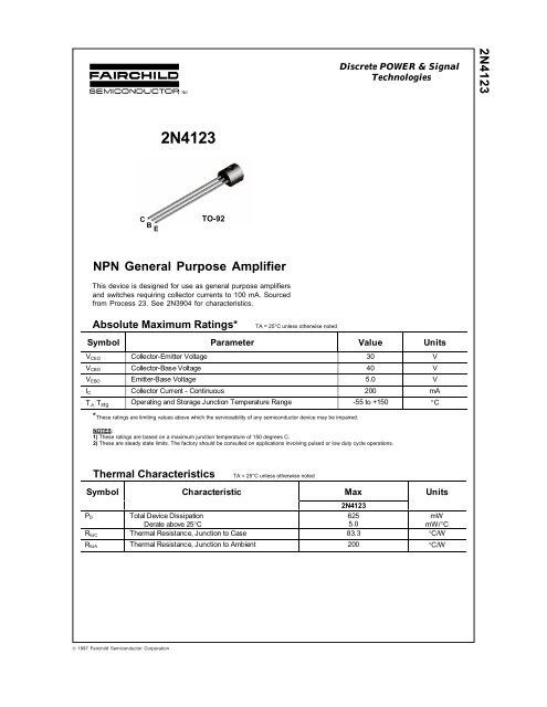
2N4123 NPN General Purpose Amplifier - Department of Physics ...
2N4123 NPN General Purpose Amplifier - Department of Physics ...
2N4123 NPN General Purpose Amplifier - Department of Physics ...

You also want an ePaper? Increase the reach of your titles
YUMPU automatically turns print PDFs into web optimized ePapers that Google loves.
Discrete POWER & Signal<br />
Technologies<br />
<strong>2N4123</strong><br />
[ ]<br />
<strong>2N4123</strong><br />
C<br />
B<br />
E<br />
TO-92<br />
<strong>NPN</strong> <strong>General</strong> <strong>Purpose</strong> <strong>Amplifier</strong><br />
This device is designed for use as general purpose amplifiers<br />
and switches requiring collector currents to 100 mA. Sourced<br />
from Process 23. See 2N3904 for characteristics.<br />
Absolute Maximum Ratings*<br />
TA = 25°C unless otherwise noted<br />
Symbol Parameter Value Units<br />
V CEO Collector-Emitter Voltage 30 V<br />
V CBO Collector-Base Voltage 40 V<br />
V EBO Emitter-Base Voltage 5.0 V<br />
I C Collector Current - Continuous 200 mA<br />
T J , T stg Operating and Storage Junction Temperature Range -55 to +150 °C<br />
*These ratings are limiting values above which the serviceability <strong>of</strong> any semiconductor device may be impaired.<br />
NOTES:<br />
1) These ratings are based on a maximum junction temperature <strong>of</strong> 150 degrees C.<br />
2) These are steady state limits. The factory should be consulted on applications involving pulsed or low duty cycle operations.<br />
Thermal Characteristics<br />
TA = 25°C unless otherwise noted<br />
Symbol Characteristic Max Units<br />
<strong>2N4123</strong><br />
P D<br />
Total Device Dissipation<br />
Derate above 25°C<br />
625<br />
5.0<br />
mW<br />
mW/°C<br />
R θJC Thermal Resistance, Junction to Case 83.3 °C/W<br />
RθJA Thermal Resistance, Junction to Ambient 200 °C/W<br />
© 1997 Fairchild Semiconductor Corporation
Electrical Characteristics<br />
TA = 25°C unless otherwise noted<br />
<strong>NPN</strong> <strong>General</strong> <strong>Purpose</strong> <strong>Amplifier</strong><br />
(continued)<br />
Symbol Parameter Test Conditions Min Max Units<br />
<strong>2N4123</strong><br />
OFF CHARACTERISTICS<br />
V (BR)CEO Collector-Emitter Breakdown Voltage* I C = 1.0 mA, I B = 0 30 V<br />
V (BR)CBO Collector-Base Breakdown Voltage I C = 10 µA, I E = 0 40 V<br />
V (BR)EBO Emitter-Base Breakdown Voltage I E = 10 µA, I C = 0 5.0 V<br />
I CBO Collector Cut<strong>of</strong>f Current V CB = 20 V, I E = 0 50 nA<br />
I EBO Emitter Cut<strong>of</strong>f Current V EB = 3.0 V, I C = 0 50 nA<br />
ON CHARACTERISTICS*<br />
h FE DC Current Gain V CE = 1.0 V, I C = 2.0 mA<br />
50 150<br />
V CE = 1.0 V, I C = 50 mA<br />
25<br />
V CE(sat) Collector-Emitter Saturation Voltage I C = 50 mA, I B = 5.0 mA 0.3 V<br />
V BE(sat) Base-Emitter Saturation Voltage I C = 50 mA, I B = 5.0 mA 0.95 V<br />
SMALL SIGNAL CHARACTERISTICS<br />
C ob Output Capacitance V CB = 5.0 V, f = 100 kHz 4.0 pF<br />
C ib Input Capacitance V EB = 0.5 V, f = 0.1 MHz 8.0 pF<br />
hfe Small-Signal Current Gain I C = 2.0 mA, V CE = 10 V,<br />
f = 1.0 kHz<br />
I C = 10 mA, V CE = 20 V,<br />
f = 100 MHz<br />
f T Current Gain - Bandwidth Product I C = 10 mA, V CE = 20 V<br />
f = 100 MHz<br />
NF Noise Figure V CE = 5.0 V, I C = 100 µA,<br />
R S = 1.0 kΩ,<br />
B W = 10 Hz to 15.7 kHz<br />
*Pulse Test: Pulse Width ≤ 300 µs, Duty Cycle ≤ 2.0%<br />
50<br />
200<br />
2.5<br />
250 MHz<br />
6.0 dB


![Cast & Crew List [Program Copy pdf] - Randolph College](https://img.yumpu.com/38268916/1/190x123/cast-crew-list-program-copy-pdf-randolph-college.jpg?quality=85)