
You also want an ePaper? Increase the reach of your titles
YUMPU automatically turns print PDFs into web optimized ePapers that Google loves.
A<br />
I Previous Page | Contents | Zoom in | Zoom out | Front Cover | Search Issue | Next Page<br />
S BE<br />
F<br />
1.26 MILLISECONDS<br />
The time by which the length of a day is estimated<br />
to have been shortened by the recent earthquake<br />
in Chile, which at 8.8 on the Richter scale ranks as the seventh strongest quake ever recorded.<br />
Chipmakers Bet on<br />
a Stacked Deck<br />
Three-dimensional packaging promises<br />
smaller, smarter gadgets<br />
Imagine that your favorite<br />
aunt lies sick on the other<br />
side of town. Rather than<br />
brave the highways to visit<br />
her, you move her into your<br />
apartment building and just<br />
ride the elevator up.<br />
Chipmakers are applying<br />
the same strategy to get<br />
around the biggest speed<br />
bump in microelectronics—<br />
the distance between dies.<br />
Instead of wiring chips to one<br />
another in two dimensions,<br />
in which the input/output<br />
plugs are spaced some<br />
200 micrometers apart,<br />
engineers plan to link them<br />
in a 3-D stack, using copper<br />
interconnects 10 μm apart—<br />
vertically. The interconnects,<br />
called through-silicon vias<br />
14 NA • IEEE SPECTRUM • APRIL 2010<br />
(TSVs), might be said to<br />
resemble elevator shafts.<br />
The hope is that TSVs<br />
will enable the industry<br />
to keep increasing the<br />
capabilities of smartphones<br />
and other gadgets while<br />
making them tinier, even<br />
as transistor densities rise<br />
at ever more sluggish rates,<br />
says Pol Marchal, a principal<br />
scientist of 3-D integration at<br />
European microelectronics<br />
R&D center Imec.<br />
To be sure, there are still a<br />
few problems. At February’s<br />
IEEE International Solid-<br />
State Circuits Conference,<br />
Imec engineers presented<br />
some key design challenges<br />
that must be overcome before<br />
TSVs can be widely used.<br />
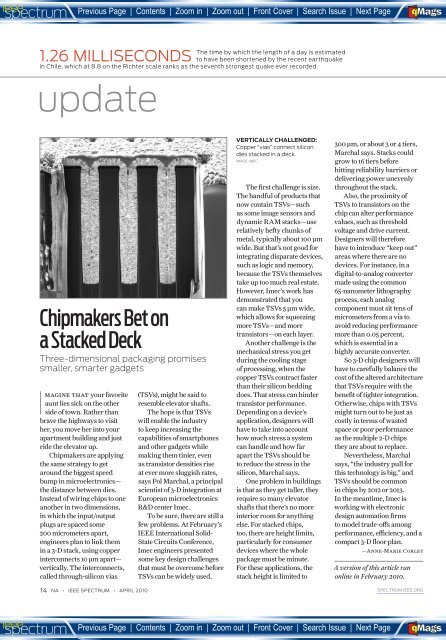
VERTICALLY CHALLENGED:<br />
Copper “vias” connect silicon<br />
dies stacked in a deck.<br />
IMAGE: IMEC<br />
The first challenge is size.<br />
The handful of products that<br />
now contain TSVs—such<br />
as some image sensors and<br />
dynamic RAM stacks—use<br />
relatively hefty chunks of<br />
metal, typically about 100 μm<br />
wide. But that’s not good for<br />
integrating disparate devices,<br />
such as logic and memory,<br />
because the TSVs themselves<br />
take up too much real estate.<br />
However, Imec’s work has<br />
demonstrated that you<br />
can make TSVs 5 μm wide,<br />
which allows for squeezing<br />
more TSVs—and more<br />
transistors—on each layer.<br />
Another challenge is the<br />
mechanical stress you get<br />
during the cooling stage<br />
of processing, when the<br />
copper TSVs contract faster<br />
than their silicon bedding<br />
does. That stress can hinder<br />
transistor performance.<br />
Depending on a device’s<br />
application, designers will<br />
have to take into account<br />
how much stress a system<br />
can handle and how far<br />
apart the TSVs should be<br />
to reduce the stress in the<br />
silicon, Marchal says.<br />
One problem in buildings<br />
is that as they get taller, they<br />
require so many elevator<br />
shafts that there’s no more<br />
interior room for anything<br />
else. For stacked chips,<br />
too, there are height limits,<br />
particularly for consumer<br />
devices where the whole<br />
package must be minute.<br />
For these applications, the<br />
stack height is limited to<br />
300 μm, or about 3 or 4 tiers,<br />
Marchal says. Stacks could<br />
grow to 16 tiers before<br />
hitting reliability barriers or<br />
delivering power unevenly<br />
throughout the stack.<br />
Also, the proximity of<br />
TSVs to transistors on the<br />
chip can alter performance<br />
values, such as threshold<br />
voltage and drive current.<br />
Designers will therefore<br />
have to introduce “keep out”<br />
areas where there are no<br />
devices. For instance, in a<br />
digital-to-analog converter<br />
made using the common<br />
65-nanometer lithography<br />
process, each analog<br />
component must sit tens of<br />
micrometers from a via to<br />
avoid reducing performance<br />
more than 0.05 percent,<br />
which is essential in a<br />
highly accurate converter.<br />
So 3-D chip designers will<br />
have to carefully balance the<br />
cost of the altered architecture<br />
that TSVs require with the<br />
benefit of tighter integration.<br />
Otherwise, chips with TSVs<br />
might turn out to be just as<br />
costly in terms of wasted<br />
space or poor performance<br />
as the multiple 2-D chips<br />
they are about to replace.<br />
Nevertheless, Marchal<br />
says, “the industry pull for<br />
this technology is big,” and<br />
TSVs should be common<br />
in chips by 2012 or 2013.<br />
In the meantime, Imec is<br />
working with electronic<br />
design automation firms<br />
to model trade-offs among<br />
performance, efficiency, and a<br />
compact 3-D floor plan.<br />
—Anne-Marie Corley<br />
A version of this article ran<br />
online in February 2010.<br />
__________<br />
SPECTRUM.IEEE.ORG<br />
A<br />
I Previous Page | Contents | Zoom in | Zoom out | Front Cover | Search Issue | Next Page<br />
S BE<br />
F<br />
aG<br />
M S<br />
aG<br />
M S