Joint Controller Development For A Humanoid Robot
Joint Controller Development For A Humanoid Robot
Joint Controller Development For A Humanoid Robot

You also want an ePaper? Increase the reach of your titles
YUMPU automatically turns print PDFs into web optimized ePapers that Google loves.
<strong>Joint</strong> <strong>Controller</strong> <strong>Development</strong> <strong>For</strong><br />
A <strong>Humanoid</strong> <strong>Robot</strong><br />
Simon Hall<br />
October 2004
Simon Christopher Hall<br />
188A Stanley Rd<br />
CARINA QLD 4152<br />
Professor Paul Bailes<br />
Head of School of Information Technology and Electrical Engineering(Acting)<br />
The University of Queensland<br />
ST LUCIA QLD 4072<br />
October 27, 2004<br />
Dear Professor Bailes,<br />
In accordance with the requirements of the Degree of Bachelor of Engineering<br />
(Mechatronic), I present the following thesis entitled, “<strong>Joint</strong> <strong>Controller</strong> <strong>Development</strong><br />
for a <strong>Humanoid</strong> <strong>Robot</strong>”. This work was performed under the supervision of Dr<br />
Gordon Wyeth.<br />
I declare that the work submitted in this thesis is my own, except were acknowledged<br />
otherwise, and has not been previously submitted for a degree at any tertiary<br />
institution.<br />
Yours Sincerely,<br />
Simon Christopher Hall<br />
2
Acknowledgements<br />
The following people deserve a word of thanks for their assistance provided during<br />
the course of this project:<br />
GuRoo, for his company during the many lonely late nights on level five in Axon<br />
building.<br />
Damien Kee, for his invaluable assistance provided throughout the year, and for his<br />
ability to be a super absorbent whinge sponge.<br />
Gordon Wyeth, for his supervision and assistance with technical issues.<br />
Geoff Walker, for his valuable assistance with power circuitry diagnostics.<br />
Keith, Dennis and Barry from the Electronics Workshop, for their assistance provided<br />
with soldering techniques and equipment use.<br />
My fellow Undergrads, for making final year engineering seem a little bit more as<br />
though you actually have a life!<br />
Lucas and Kelly, for all the much appreciated cooked dinners left in the fridge, and<br />
for doing all the grocery shopping.<br />
My family and friends, for their much appreciated support throughout the year.<br />
3
Abstract<br />
The focus of this thesis is the development of DC motor controller boards for UQ’s<br />
humanoid robot, “GuRoo”. With the project now in its fourth year of development,<br />
the original lower limb DC motor controller boards were in need of an upgrade. A<br />
new hardware design was finalised in late 2003. Over the course of 2004, the<br />
progressive construction and testing of these new boards has brought them from blank<br />
PCB’s to near fully operational status.<br />
The new design incorporates a Motorola 68376 DSP superior to the Texas<br />
Instruments TMS320F243 processor controlling the old boards. This thesis details the<br />
progressive programming and testing of the new boards performed to achieve near<br />
full functionality. Software was developed to utilise pulse width modulation(PWM)<br />
and quadrature decoding capabilities of the 68376’s TPU(Timer Processor Unit).<br />
Code was also developed to make use of the new processor’s TouCAN(<strong>Controller</strong><br />
Area Network) and QADC(Queued Analog to Digital Converter) modules. After<br />
verifying correct operation of these functionalities, the existing software of the<br />
original 2001 boards was updated to suit the new design.<br />
An initialisation routine was developed for GuRoo’s joint positioning on power-up.<br />
This was achieved through position control of GuRoo’s motors about encoder index<br />
pulses. CAN communication enables the robots joints to be incremented between<br />
successive index positions.<br />
Software was developed to demonstrate the new boards functionality, including the<br />
index positioning initialisation. This demonstration software proved that the control<br />
loop speed can now be drastically increased.<br />
Through harnessing the new board's superior capabilities, further work following this<br />
thesis will enable GuRoo's joint control performance to be enhanced.<br />
4
Table of Contents<br />
Acknowledgements____________________________________________________3<br />
Abstract_____________________________________________________________4<br />
Table of Contents _____________________________________________________5<br />
List of Figures and Tables______________________________________________7<br />
1. Introduction_____________________________________________________9<br />
1.1 RoboCup ________________________________________________________ 9<br />
1.2 Thesis Goals and Overview ________________________________________ 10<br />
2. GuRoo’s <strong>Joint</strong> Control ___________________________________________12<br />
2.1 A History of GuRoo’s <strong>Joint</strong> Control <strong>Development</strong> _____________________ 12<br />
2.2 GuRoo’s Existing <strong>Joint</strong> Control ____________________________________ 14<br />
2.2.1 Degrees of Freedom & Board Locations ___________________________________14<br />
2.2.2 CAN Communication Network __________________________________________15<br />
2.2.3 Motor Control Process _________________________________________________17<br />
2.2.4 Pulse Width Modulation(PWM) – Bipolar and Unipolar Topologies _____________17<br />
2.2.5 Motor Drive – The H-bridge_____________________________________________19<br />
2.2.6 PI Velocity Control Implementation_______________________________________20<br />
2.2.7 Quadrature Decoding __________________________________________________21<br />
2.3 Existing Control Software for GuRoo’s Lower Limb Boards ____________ 22<br />
2.3.1 PWM Duty Cycle Feathering ____________________________________________23<br />
2.4 2001 <strong>Controller</strong> Design Flaws ______________________________________ 24<br />
2.4.1 Control Loop Speed ___________________________________________________24<br />
2.4.2 Power Consumption ___________________________________________________25<br />
2.4.3 Implementation of Design ______________________________________________25<br />
2.4.4 Lack of Initialisation Software ___________________________________________26<br />
2.5 2004 Lower Limb <strong>Controller</strong> Design ________________________________ 26<br />
2.5.1 Microcontroller_______________________________________________________26<br />
2.5.2 Memory Setup _______________________________________________________27<br />
2.5.3 Motor Driver Circuitry _________________________________________________28<br />
2.5.3.1 H-bridge Design ___________________________________________________28<br />
2.5.3.2 MOSFET Driver Design _____________________________________________29<br />
2.5.4 Current Sensing and Motor Protection _____________________________________30<br />
2.5.5 Power Supply ________________________________________________________31<br />
2.5.6 Communication ______________________________________________________32<br />
2.5.7 Additional Features____________________________________________________33<br />
2.5.8 Board Layout and Placement ____________________________________________34<br />
3. <strong>Development</strong> of the 2004 <strong>Controller</strong> Boards __________________________35<br />
3.1 Board <strong>Development</strong> Plan__________________________________________ 35<br />
3.2 Configuring the Motorola 68376 ___________________________________ 36<br />
3.2.1 Initial Hardware Issues _________________________________________________36<br />
3.2.2 System Clock Speed ___________________________________________________37<br />
3.3 Memory Map ___________________________________________________ 37<br />
3.4 Serial Communication <strong>Development</strong> ________________________________ 38<br />
3.5 Timer Processor Unit <strong>Development</strong> _________________________________ 39<br />
3.5.1 Pulse Width Modulation Generation ______________________________________40<br />
5
3.5.2 Quadrature Decoding __________________________________________________41<br />
3.6 Current Sensing <strong>Development</strong> _____________________________________ 42<br />
3.6.1 Configuring the Analog to Digital Converter ________________________________42<br />
3.6.2 Conversion Times_____________________________________________________43<br />
3.6.3 Resolution of Current Sensing ___________________________________________45<br />
3.6.4 Current Sensing Testing ________________________________________________46<br />
3.6.5 Calibration of Current Sensing & Motor Torque Correlation____________________47<br />
3.7 CAN Communication <strong>Development</strong> _________________________________ 49<br />
3.7.1 TouCAN Module Configuration__________________________________________50<br />
3.7.2 Message Transmission & Reception_______________________________________51<br />
3.7.3 CAN Software Implementation __________________________________________52<br />
3.8 MOSFET Driver Issues ___________________________________________ 54<br />
3.9 2004 Lower Limb <strong>Controller</strong> Power Consumption ____________________ 55<br />
4. 2004 <strong>Controller</strong> Software _________________________________________56<br />
4.1 Updated Software________________________________________________ 57<br />
4.1.1 startup.c and socpwr.as _______________________________________________57<br />
4.1.2 lowlevel.c___________________________________________________________58<br />
4.1.2.1 set_PWM() ______________________________________________________59<br />
4.1.2.2 read_curr() ____________________________________________________61<br />
4.1.2.3 read_enc() _____________________________________________________62<br />
4.1.2.4 transmitShort() and transmitChar() _________________________62<br />
4.1.2.5<br />
4.1.3<br />
outputToLEDs()_________________________________________________62<br />
Additional Code for the New Processors ___________________________________62<br />
4.2 Initialisation Code _______________________________________________ 64<br />
4.2.1 Index Position Control _________________________________________________64<br />
4.2.2 Index Position Control Performance_______________________________________66<br />
4.3 Demonstration Software __________________________________________ 68<br />
4.3.1 Control Loop Demonstration Code________________________________________68<br />
4.3.2 PI Velocity Control Loop Processing Time _________________________________70<br />
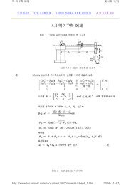
4.4 Memory Consumption____________________________________________ 71<br />
5. Thesis Outcomes and Conclusion __________________________________72<br />
6. The Road Ahead ________________________________________________73<br />
References _________________________________________________________75<br />
Appendix A - Updated 2004 <strong>Controller</strong> Board 1-5 Schematic _________________77<br />
Appendix B - Updated 2004 <strong>Controller</strong> Board 6 Schematic __________________78<br />
Appendix C – Board Layout & Placement ________________________________79<br />
Appendix D - 2004 <strong>Controller</strong> Software __________________________________80<br />
6
List of Figures and Tables<br />
Figure 1.1: GuRoo The <strong>Humanoid</strong> <strong>Robot</strong> 9<br />
Figure 1.2: Robocup. <strong>Humanoid</strong> Soccer - A Goal for 2050. [8] 10<br />
Table 2.1: Past Theses Relating to GuRoo’s <strong>Joint</strong> Control. 12<br />
Figure 2.1: The PUMA Arm(left) & Kennedy’s Distributed<br />
<strong>Controller</strong> Design(right). [4] 13<br />
Figure 2.2: 2001 Lower Limb Motor <strong>Controller</strong> Board. [4] 14<br />
Figure 2.3: The 23 Degrees of Freedom in GuRoo’s Body. [1] 15<br />
Figure 2.4: Board Placement in GuRoo’s Body. [3] 15<br />
Figure 2.5: Flow of Control/Communication in GuRoo. [9] 16<br />
Figure 2.6: CAN Data Frame. [11] 16<br />
Figure 2.7: Block Diagram of <strong>Controller</strong> Board Components<br />
and Signal Flow. [3] 17<br />
Figure 2.8: Bipolar PWM(above) and Unipolar PWM(below). [3] 18<br />
Figure 2.9: A Simplified H-bridge Configuration. 20<br />
Figure 2.10: Implementation of PI Control in the Lower Limb <strong>Controller</strong>s. 21<br />
Figure 2.11: Encoder Waveforms for <strong>For</strong>ward and Reverse<br />
Position Feedback. [13] 21<br />
Figure 2.12: Block diagram of 2001 <strong>Controller</strong> Code. [3] 22<br />
Figure 2.13: 2004 <strong>Controller</strong> H-bridge Design. 28<br />
Figure 2.14: 2004 <strong>Controller</strong> H-bridge Driver Design. 29<br />
Table 2.2: Truth Table for Input Logic to MOSFET Drivers. 29<br />
Figure 2.15: 2004 <strong>Controller</strong> Current Sensing Circuitry. 30<br />
Figure 2.16: Lower Limb Board Power Circuitry. 31<br />
Figure 2.17: CAN Communication Circuitry(left). QSPI and<br />
RS232 Headers (right). 33<br />
Figure 2.18: ICD Programmer - In System Programming. 33<br />
Figure 3.1: Original Reset Conditioning Circuitry. 37<br />
Figure 3.2: Internal and External Memory Addressing on the Motorola 68376. 38<br />
Figure 3.3: RS232 Connector for Board to PC Serial Communication. 39<br />
Figure 3.4: TPU Generating PWM (~100kHz, 20% duty cycle). 41<br />
Figure 3.5: TPU Generating PWM (~50kHz, 50% duty cycle). 41<br />
Figure 3.6: QADC Q-CLK Duty Cycle. 43<br />
Figure 3.7: AD Conversion Timing. [5] 43<br />
Figure 3.8: Time Taken for a Single AD Conversion. 44<br />
Figure 3.9: Time Taken <strong>For</strong> Six Consecutive AD Conversions. 45<br />
Figure 3.10: ADC Conversions for 50khz PWM, 50% duty cycle. 46<br />
Figure 3.11: AD Conversion for 50khz PWM, 100% duty cycle. 47<br />
Figure 3.12: Attempted Current Sensing and Torque Correlation Test Apparatus. 48<br />
Figure 3.13: CAN Bit Timing Parameters. [11] 50<br />
Figure 3.14: Standard CAN Message Buffer Structure. [5] 51<br />
7
Figure 3.15: Transmission of a Velocity Profile CAN Frame. 53<br />
Figure 3.16: Re-routing of the MOSFET Driver Disable Lines. 54<br />
Table 3.1: 2004 <strong>Controller</strong> Power Consumption. 55<br />
Figure 4.1: Interaction of Software on the 2004 <strong>Controller</strong>s. 56<br />
Figure 4.2: PWM Feathering Waveform for a Duty Cycle<br />
of “1” with 50kHz PWM 60<br />
Figure 4.3: Register Addressing – Mapped by mc68376.h. [5] 63<br />
Figure 4.4: Flowchart for Index Positioning Initialisation. 65<br />
Figure 4.5: Position Control Loop Processing Time. 67<br />
Table 4.1: Repeatability of Index Positioning. 67<br />
Figure 4.6: Visual Verification of Index Positioning Repeatability<br />
with a Scribed Mark. 68<br />
Figure 4.7: Demonstrating the New Software – Initialisation and<br />
Velocity Control. 69<br />
Figure 4.8: 1kHz PI Velocity Control Loop Processing Time<br />
(No AD Conversions). 70<br />
Figure 4.9: 1kHz PI Velocity Control Loop Processing Time<br />
(6 AD Conversions Per Loop). 71<br />
Figure 5.1: The New 2004 Lower Limb <strong>Controller</strong> Board. 72<br />
8
1. Introduction<br />
Research and development of humanoid robot technology is more than just a novel<br />
idea. <strong>Robot</strong>s might not be widespread in today’s society, but where they do exist their<br />
presence can be very beneficial, e.g., rescue robots performing tasks in environments<br />
that may be hazardous to human life. Reliable manoeuvrability and interaction of a<br />
robot within its environment is a common problem for any robotics project. Humans<br />
have contributed to this problem by adapting the world around us to suit our own<br />
geometries and capabilities. It therefore makes sense that the more human like a robot<br />
is, the easier it will be able to interact with us and our environment. Hence the reason<br />
for humanoid development is well justified.<br />
The University of Queensland’s humanoid<br />
robot, GuRoo, has been an ongoing project<br />
since 2001. Weighing in at 38kg, this 1.2m tall<br />
humanoid is fully autonomous, with the ability<br />
to crouch, stand on one leg and walk unaided at<br />
a speed of 0.1m/s. Now in its fourth year of<br />
development, this project involves the efforts<br />
of a large team of undergraduate and<br />
postgraduate students and staff of UQ. <strong>Joint</strong><br />
control in particular, has proved to be a major<br />
focus of GuRoo’s development.<br />
Figure 1.1: GuRoo The <strong>Humanoid</strong> <strong>Robot</strong><br />
GuRoo’s original lower limb joint design was constructed in 2001. Since then, a new<br />
superior design has been developed. The topic of this thesis is the development and<br />
testing of this new design.<br />
1.1 RoboCup<br />
The immediate purpose of GuRoo is to participate in the International Robocup<br />
Competition, an ongoing quest to develop soccer playing humanoid robots by the year<br />
2050.<br />
9
Figure 1.2: Robocup. <strong>Humanoid</strong> Soccer - A Goal for 2050. [8]<br />
RoboCup officially began in 1997, with the humanoid league of the competition<br />
commencing in 2002. The humanoid competition has included challenges such as<br />
walking, balancing, standing on one leg and freestyle. GuRoo competed in 2002 with<br />
respectable success. He obtained 7 th place in the walking competition and the freestyle<br />
competition, and was the best competitor in the “stand on one leg” event [6]. Active<br />
joint control played a major part in GuRoo’s success.<br />
1.2 Thesis Goals and Overview<br />
The primary goal of this thesis was to develop GuRoo’s new 2004 lower limb DC<br />
motor controller boards to an operational status, sufficient for installation into<br />
GuRoo’s existing system. Achieving this goal required building the new boards from<br />
blank PCB’s whilst simultaneously developing software for the new board’s Motorola<br />
68376 DSP. Unfortunately, due to time constraints this goal has not been completely<br />
achieved. At present the boards are at a stage where they are almost ready for<br />
installation. A few more hardware and software issues require finalisation before<br />
installation may take place. Details of these minor issues will be discussed throughout<br />
this document.<br />
A secondary goal for this thesis was to develop software for these new boards that<br />
would initialise each joint on power-up of the robot. Prior to this thesis, an<br />
initialisation process was non-existent. It was requested that initialisation purely<br />
involve the positioning of joints to encoder index pulses. A successful initialisation<br />
10
outine has been developed that uses CAN to command each joint to increment to<br />
encoder index pulse positions.<br />
This thesis has also intended to serve as a document which collates details of the new<br />
design and its features, and the design decisions that were made in order to justify its<br />
existence.<br />
Chapter Two briefly outlines the history of GuRoo’s joint control and provides a short<br />
description of the operation of the lower limb joint control. This is followed by a brief<br />
description of the new 2004 lower limb controller board design.<br />
Chapter Three discusses the board development process required to achieve the<br />
required functionality.<br />
Chapter Four Details the new software developed. This includes the updates that have<br />
been required for the existing software to suit the 68376, and the implementation of<br />
the new initialisation routine.<br />
Chapter Five concludes this document, and discusses the outcomes of this thesis.<br />
Chapter Six gives a brief outline of the further work that is required before the boards<br />
can be installed into GuRoo. It also discusses ideas for further development of the<br />
new joint controllers.<br />
11
2. GuRoo’s <strong>Joint</strong> Control<br />
2.1 A History of GuRoo’s <strong>Joint</strong> Control <strong>Development</strong><br />
The past three years have seen a major contribution of work towards developing<br />
GuRoo’s joint control. The past theses that have directly influenced GuRoo’s 2004<br />
joint controller design are listed in Table 2.1.<br />
Thesis Title Author Year Completed<br />
Design and Implementation of a James Kennedy 1999<br />
Distributed Digital Control System<br />
in an Industrial <strong>Robot</strong>.<br />
Design of DC Motor <strong>Controller</strong>s for Jarad Stirzaker 2001<br />
a <strong>Humanoid</strong> <strong>Robot</strong><br />
Design & Implementation of Small Tim Cartwright 2001<br />
Scale <strong>Joint</strong> <strong>Controller</strong>s for a<br />
<strong>Humanoid</strong> <strong>Robot</strong><br />
Distributed Motion <strong>Controller</strong>s for Andrew Hood 2002<br />
a <strong>Humanoid</strong> <strong>Robot</strong><br />
Gait Generation & Control Adam Drury 2002<br />
Algorithms for a <strong>Humanoid</strong> <strong>Robot</strong><br />
Mobile <strong>Robot</strong> Electrical Design Doug Turk 2003<br />
Table 2.1: Past Theses Relating to GuRoo’s <strong>Joint</strong> Control.<br />
In 1999, James Kennedy[12] designed hardware and software for a distributed control<br />
system for actuation of a Kawasaki PUMA 560 industrial robot arm as shown in<br />
Figure 2.1. Kennedy’s distributed control system consisted of a network of DC motor<br />
control boards distributed throughout the robot, with each board situated as close as<br />
possible to the motors it controlled. The joint control design that existed in the PUMA<br />
arm prior to his design utilised complex control electronics, with a bulky unreliable<br />
cable driving each joint from a central controller. Kennedy’s design resulted in a<br />
simplified, more reliable joint control system, with a major reduction in the<br />
complexity and cost of the wiring harness. In many ways, Kennedy’s design became<br />
12
the foundation for the control system that exists in GuRoo and the subsequent new<br />
2004 design.<br />
Figure 2.1: The PUMA Arm(left) & Kennedy’s Distributed <strong>Controller</strong> Design(right). [4]<br />
GuRoo’s original and existing joint controller hardware was designed and developed<br />
by Stirzaker[4] and Cartwright[15] in 2001. Stirzaker’s thesis focused on the design<br />
of the lower limb controller boards, as shown in Figure 2.2, for the control and<br />
actuation of GuRoo’s fifteen lower limb Maxon DC motors. Cartwright’s thesis<br />
focused on the development of an upper limb control board which actuates the eight<br />
light-weight servo motors in GuRoo’s upper body. There were many consistencies<br />
between Stirzaker and Cartwright’s designs. Stirzaker’s lower limb design was then<br />
made fully operational by Hood[3] and Drury[6] in 2002. Hood’s work focused on the<br />
development of low level software for control of the lower limb boards while Drury<br />
developed software for the PI velocity control algorithm and velocity profiles for gait<br />
patterns.<br />
Hood also performed a complete review of the existing lower limb controller boards,<br />
and made specifications for a new board design. Finally, in Nov 2003, Kee[9]<br />
designed and manufactured the joint controller PCB used in this thesis. This finalised<br />
design incorporated the same microcontroller and memory configuration that is to be<br />
13
incorporated into Turk’s[13] new electrical design for UQ’s mobile soccer playing<br />
robot project, the RoboRoo’s.<br />
Figure 2.2: 2001 Lower Limb Motor <strong>Controller</strong> Board. [4]<br />
2.2 GuRoo’s Existing <strong>Joint</strong> Control<br />
GuRoo’s gait’s are implemented by a distributed control system. Movement patterns<br />
are generated by an external computer. The external computer communicates with the<br />
various motor controller boards throughout its body. Each motor controller then<br />
processes the instructions it receives, to regulate each motor’s speed such that<br />
GuRoo’s body moves in a desired fashion.<br />
2.2.1 Degrees of Freedom & Board Locations<br />
Overall, there are currently 23 joints or “degrees of freedom” in GuRoo’s body, as<br />
outlined in Figure 2.3. A DC motor actuates each joint. The neck, shoulder and elbow<br />
joints are actuated by eight, low power, low weight Hi-Tech HS705-MG RC servo<br />
motors. The lower limbs are actuated by more powerful, Maxon 70W RE32 brushed<br />
DC motors, fifteen in total. [17]<br />
All 23 of these motors are controlled by six boards spread throughout GuRoo’s<br />
chassis. Their locations are indicated in Figure 2.4. One motor controller board<br />
14
(Board 6) is located on the back of the torso controlling all eight upper joints, while<br />
the lower limb controllers (Boards 1 to 5) are located as follows:<br />
- One board in the stomach, controlling the three waist joints.<br />
- One board in each thigh controlling the three respective hip joints.<br />
- One board in each ankle controlling the respective knee and two ankle joints.<br />
Figure 2.3: The 23 Degrees of<br />
Freedom in GuRoo’s body. [1]<br />
Figure 2.4: Board Placement<br />
in GuRoo’s Body. [3]<br />
Each lower limb motor controller board controls three motors. Desired joint velocities<br />
are transmitted through serial communication from an external computer to Board 6.<br />
The signals are then transmitted to each of the lower limb controllers through a<br />
<strong>Controller</strong> Area Network(CAN) serial communication protocol.<br />
2.2.2 CAN Communication Network<br />
CAN is a multi-master system with software identifiable nodes. Utilising a simple<br />
two-wire bus, the standard includes sophisticated error checking and a high bandwidth<br />
of up to 1Mbps [3]. Figure 2.5 outlines the flow of communication in GuRoo. When a<br />
message is sent through CAN, it is broadcast to all nodes, and software defineable<br />
message buffers at each node either accept or reject messages. Nodes are software<br />
programmable for message reception.<br />
15
CAN BUS<br />
Spine Board<br />
Head & Arms Board<br />
Right Hip Board<br />
SERIAL<br />
Left Hip Board<br />
EXTERNAL<br />
COMPUTER<br />
Right Leg Board<br />
Left Leg Board<br />
Figure 2.5: Flow of Control/Communication in GuRoo. [9]<br />
Figure 2.6: CAN Data Frame. [11]<br />
Figure 2.6 outlines a CAN data frame. Each CAN frame can contain up to 8 bytes of<br />
data. The Arbitration(ID) field forms the first part of every message sent across a<br />
CAN network. Message prioritisation in the event of multiple nodes sending messages<br />
synchronously is given to the message with the lowest ID field. In GuRoo’s<br />
communication network, each board has software defined CAN message buffers that<br />
will either accept or reject messages sent to them. This allows each board not only to<br />
receive the applicable incoming desired velocity settings but also to transmit<br />
performance information back to the external computer.<br />
16
CAN makes use of a two wire bus, CANH (high) and CANL (low). The CAN bus can<br />
be placed in two states, dominant and recessive. In the dominant state both lines are<br />
driven to 2.5V, and when recessive, CANH is driven to 5V and CANL is driven to<br />
0V. When a message is converted into CAN format, logical one bits are referred to as<br />
recessive bits and logical zero bits are referred to as dominant bits.<br />
2.2.3 Motor Control Process<br />
On reception of incoming desired motor velocity settings, the motor controllers<br />
perform all low level control. Less powerful processors are required and<br />
communication complexity is reduced through the local computation of motor control<br />
[12].<br />
Figure 2.7 shows a block diagram of the lower limb motor controller board signal<br />
flow. Desired joint velocities arrive at each board at 50Hz from the CAN bus and are<br />
fed into the DSP message buffers. The DSP then uses these desired speed settings to<br />
run a PI velocity control loop at 250Hz. Motor drive is governed by pulse width<br />
modulation (PWM) of motor voltage. Feedback of motor current and motor position<br />
sensing allows for closed loop control of motor speeds.<br />
Figure 2.7: Block Diagram of <strong>Controller</strong> Board Components and Signal Flow. [3]<br />
2.2.4 Pulse Width Modulation(PWM) – Bipolar and Unipolar Topologies<br />
Velocity control is achieved through varying the voltage across the terminals of a<br />
motor. Pulse Width Modulation is the continuous fast switching of motor voltage. By<br />
varying the duty cycle from 0% to 100%, the effective voltage across a motor can be<br />
established from a set input voltage (V motor ) .<br />
17
Two basic topologies for the implementation of PWM are unipolar PWM and bipolar<br />
PWM. As described in Figure 2.8, bipolar PWM involves the switching of voltage<br />
between a positive and a negative set voltage(V motor ) . Under this configuration a net<br />
positive voltage across the motor can be achieved for a positive duty cycle greater<br />
than 50%. This will drive the motor forward, provided that generated torque is greater<br />
than load torque. In the opposite case, if the net voltage across the motor is negative,<br />
the motor will be driven in reverse, provided that generated torque is greater than load<br />
torque. If the duty cycle is maintained at 50% the motor will remain stationary,<br />
provided there is no load torque applied.<br />
Figure 2.8: Bipolar PWM(above) and Unipolar PWM(below). [3]<br />
Unipolar PWM involves only switching the voltage across the motor between 0 and<br />
V motor or –V motor to achieve forward and reverse motion respectively. If a duty cycle of<br />
18
0 is applied, the motor will remain stationary, again provided that the motor is<br />
unloaded.<br />
The advantage of unipolar PWM is that ripple current can be significantly lower than<br />
that for bipolar switching. Ripple current is related to the inductance of the armature<br />
and the voltage ripple component of voltage across the motor’s armature[16]:-<br />
v r ≈ L a (di r /dt)<br />
where v r = the voltage ripple component of armature voltage (V).<br />
L a = armature inductance (H).<br />
i r = the current ripple component of armature current (A).<br />
Bipolar PWM effectively doubles the voltage swing across the motor terminals and<br />
drastically increases the voltage ripple component of armature voltage and<br />
consequently the ripple current. Power losses associated with this ripple current<br />
are[16]:-<br />
P ∆I = R a (I r ) 2<br />
where R a = armature resistance (Ω).<br />
I r = RMS value of the current ripple component (A).<br />
Observation of this I r<br />
2<br />
relationship entails that power losses associated with ripple<br />
current can be significantly reduced by lowering the ripple current .<br />
2.2.5 Motor Drive – The H-bridge<br />
PWM is implemented through the use of an H-bridge. A simplified H-bridge<br />
configuration is shown in Figure 2.9. By varying switch states, the motor can be<br />
placed in the following states:<br />
19
1) Driving forward (T1 on, T4 on)<br />
2) Driving in reverse (T2 on, T3 on)<br />
3) Braked to ground (T3 on, T4 on)<br />
4) Braked to V motor (T1 on, T2 on)<br />
5) Neutral/ Floating (all switches off)<br />
Figure 2.9: A Simplified H-bridge Configuration.<br />
Bipolar switching only makes use of states 1 and 2. Unipolar switching involves states<br />
1 and 2 and one of either 3 or 4. GuRoo’s original control boards implemented bipolar<br />
PWM.<br />
2.2.6 PI Velocity Control Implementation<br />
PI, Proportional plus Integral velocity control is achieved through digital feedback<br />
from each motor, gearbox and encoder unit. As shown in Figure 2.10, input PWM<br />
duty cycles are fed to motor terminals proportional and integral to the error between<br />
the desired input velocity profile and the actual motor velocity. Motor velocities are<br />
expressed as functions of the difference in motor position per control loop. The<br />
integral component removes the steady state error in velocity control.<br />
20
Figure 2.10: Implementation of PI Control in the Lower Limb <strong>Controller</strong>s.<br />
2.2.7 Quadrature Decoding<br />
Feedback of motor position is achieved through Quadrature Decoding of encoder<br />
position. Encoders are attached to each motor’s rotating shaft. Quadrature decoding<br />
enables relative motor positions to be deciphered through the incrementing or<br />
decrementing of forward and reverse encoder counts respectively. This is achieved<br />
through the processing of two pulsating, 90 degree, out of phase waveforms(channels)<br />
output from each encoder. As described in Figure 2.11, if Channel A is leading, the<br />
motor is rotating clockwise and if Channel B is leading, the motor is rotating anticlockwise.<br />
Figure 2.11: Encoder Waveforms for <strong>For</strong>ward and Reverse Position Feedback. [13]<br />
21
The encoders on GuRoo’s lower limbs are each accompanied by 500 pulse per<br />
revolution encoders. The existing system decodes for each channel on both rising and<br />
falling edges, to give a resolution of 2000 counts per revolution. This is then<br />
transferred through a 156:1 gearhead which gives a total theoretical resolution of<br />
0.00115 degrees per revolution.<br />
2.3 Existing Control Software for GuRoo’s Lower Limb Boards<br />
Operation of the existing joint controller code required closed loop control of joint<br />
velocities as outlined in Figure 2.12. All code is written in C++ which is compiled<br />
down to machine language and ported to the flash memory of the microcontrollers.<br />
The 2001 boards are each controlled by a Texas Instruments TMS320F243 16 bit<br />
DSP.<br />
When GuRoo is first switched on, control of each motor is initiated by the main()<br />
function in startup.c. This source file initialises the DSP’s appropriate register values<br />
and sets up a periodic interrupt that calls b1_control() in board1.c.<br />
b1_control() is the function that implements the PI velocity control algorithm.<br />
Figure 2.12: Block Diagram of 2001 <strong>Controller</strong> Code. [3]<br />
22
The code has been kept modular so that all firmware code(lowlevel.c, can.c and<br />
startup.c) can be updated without modifiying the control algorithm code. What this<br />
means is that board1.c(b1_control()) requires no alteration. b1_control() is<br />
also used by the simulator and therefore maintaining this code as a separate module<br />
enables it to be used by both systems.<br />
b1_control() achieves PI velocity control by calling upon methods in<br />
lowlevel.c and can.c. <strong>For</strong> each particular motor, the can_receive() function<br />
supplies the desired velocity from the CAN bus and the read_enc() function<br />
supplies the current encoder reading. From the desired velocity and current encoder<br />
reading, b1_control() dictates an estimate of the required PWM setting to<br />
achieve the desired velocity. This required PWM setting is set via the set_pwm()<br />
function.<br />
The purpose of the read_curr() function is to continually monitor the armature<br />
current of each motor and if required, alter the required PWM setting to a maximum<br />
safe setting that will not damage the motor. This feature is currently not utilised on the<br />
2001 boards.<br />
2.3.1 PWM Duty Cycle Feathering<br />
In 2001 Hood discovered that when low duty cycles were required there was not<br />
enough resolution for duty cycle settings. Originally, PWM duty cycle had a<br />
resolution of -100 to 100 for full reverse and full forward motion respectively<br />
(actually a number from 0 to 200 – Bipolar PWM). Under the direction of Dr Gordon<br />
Wyeth, a procedure called “feathering” was implemented to give finer resolution.<br />
An integer between -1600 and 1600 is passed as a parameter for desired duty cycle.<br />
The lower four bits of this number are masked off to give a “feather_count” between<br />
0 and 15. What remains is a duty value between -100 and 100. A “pwm_low” is then<br />
assigned as that duty value between 0 and 100 and a “pwm_high” value is assigned as<br />
that duty value plus one (or -1, if the duty value is between 0 and -100). The 100kHz<br />
timer which in fact generates the PWM, enables a counter to be incremented every<br />
10us. If feather_count is less than counter, the duty cycle is set to pwm_high. If the<br />
23
feather_count is less than counter, the duty cycle is set to pwm_low. When counter<br />
reaches 16 it is reset to 0.<br />
The overall effect is that the PWM duty cycle can be passed a decimal amount<br />
between -100 and 100. The decimal value consists of feather_count / 16.<br />
2.4 2001 <strong>Controller</strong> Design Flaws<br />
The design specifics of the old controller boards will not be mentioned in this<br />
document. <strong>For</strong> a detailed description of the full 2001 design refer to Stirzaker[4].<br />
Only the components of their design that impeded board performance will be<br />
described here.<br />
Based upon Hood’s analysis of the 2001 design, the following discussion outlines the<br />
flaws of the 2001 lower limb controllers. It is these issues that necessitated the design<br />
of the new 2004 controller boards.<br />
2.4.1 Control Loop Speed<br />
After the development of control code by Drury and Hood in 2002, it was found that<br />
the control loop was not able to operate at Stirzaker’s originally anticipated speed of<br />
2kHz. This was mainly due to limitations of the 2001 controller’s CPU. The Texas<br />
Instruments TMS320F243 processors are only equipped with a single quadrature<br />
decoder channel. Since each board was required to control three motors, a single<br />
channel was not enough.<br />
To compensate for this Stirzaker designed his boards to have two external quadrature<br />
decoders. These IC’s process the encoder pulses and feed 16 bit encoder count values,<br />
one byte at a time, into the TMS chip via its data bus. This proved to be a major<br />
bottleneck for the control loop algorithm.<br />
The end result is that each control loop actually requires 1.28ms to process, and thus<br />
4ms(250Hz) has been allowed for each loop in order to cater for additional serial<br />
feedback of sensor data to an external computer for analysis. [3]<br />
24
2.4.2 Power Consumption<br />
The 2001 controllers feature motor drive circuitry that consumes power inefficiently.<br />
Stirzaker chose an integrated motor driver circuitry package for the H-bridge<br />
circuitry, the L6203 from ST. Unfortunately these packages were found to very<br />
inefficient, requiring the dissipation of a large amount of heat. This required the<br />
mounting of large heat sinks adding weight to GuRoo’s lower limbs. Hood’s work<br />
uncovered that losses in the L6203 were mainly conduction losses of the switching<br />
devices within due to their large on resistance(R ON ). [3]<br />
The L6203 package also required the use of bipolar switching, which as stated in<br />
section 2.2.4 is a relatively inefficient switching method. When GuRoo was first<br />
powered up, it was found that there were so much conduction losses that within<br />
minutes the MAXON motors became hot to touch. This was reduced by introducing<br />
separate inductors in series with the motors, proving that most of the losses were due<br />
to a large amount of ripple current dissipation. This halved the ripple current and the<br />
motors ran cold, but the addition of extra inductors also added unnecessary weight to<br />
GuRoo’s lower limbs. [3]<br />
T rectify these problems, Hood made design specifications for a more efficient semidiscrete<br />
motor driving circuitry.<br />
2.4.3 Implementation of Design<br />
The PCB layout of the 2001 controllers needed review. Positioning of the components<br />
on the board was found to be poor. There was a large amount of wasted space and few<br />
useful test points. Placing clip test leads to ground on the boards was inconvenient.<br />
The DSP itself was difficult to access. Motor power headers were not placed in order,<br />
which posed a possible threat to wiring up motors incorrectly. There was also a lack<br />
of debugging LED’s on the board. The wiring harness proved to be complicated and<br />
impractical. [3]<br />
25
2.4.4 Lack of Initialisation Software<br />
It was found by Hood that initialisation of the robot prior to starting a gait routine was<br />
impractical. Power would be applied to GuRoo while on its stand followed by placing<br />
it on the ground and the positioning of each joint by eye[3]. A very time consuming<br />
and potentially difficult process.<br />
Propositions for an initialisation routine have been made prior to this thesis. The<br />
original plan was to use mechanical stops or switches and driving GuRoo’s limbs to<br />
their mechanical limits followed by retraction to a set point. Hood proposed an optical<br />
sensor alignment scheme.It was decided that this would add unnecessary complexity<br />
to the system.<br />
Instead it was decided that utilising the index pulses of the encoders would provide a<br />
means for initialisation. Index pulse initialisation was achieved as part of this thesis<br />
and the successful results of a routine developed to do so are discussed in section 4.2.<br />
2.5 2004 Lower Limb <strong>Controller</strong> Design<br />
This section outlines the fundamental components of the new design. The full<br />
schematic is contained in Appendix A for board’s 1-5 and Appendix B for board 6.<br />
Note that this schematic has been updated to include the adaptions made during the<br />
course of this thesis. The details of the adaptations made will be explained further in<br />
section 3.<br />
2.5.1 Microcontroller<br />
The microcontroller chosen for the new boards is the Motorola MC68376. It was in<br />
fact the original desired processor by Stirzaker & Cartwright in 2001, but due to cost<br />
and availability was not chosen [4]. Hood also outlined its superior aspects when<br />
considering processor selection for a new controller design. This processor has the<br />
following features:<br />
26
- 32 bit architecture.<br />
- On board TPU(Timer Processing Unit) with which 16 pins can be individually<br />
programmed to use its capture register (to decode quadrature pulses) or<br />
compare register (for PWM generation).<br />
- Analog to Digital Converter for current sensing.<br />
- TouCAN communication module.<br />
- Operating speeds of up to 21MHz.<br />
The most advantageous of these features is the TPU module’s capabilities. It features<br />
16 independent timer channels. This allows for three PWM outputs and six quadrature<br />
decoding lines(two are required for each encoder) leaving seven TPU lines to spare.<br />
This addresses the former quadrature decoding bottleneck as raised by Hood, of the<br />
2001 controllers.<br />
Note that Hood also expressed desirability for this processor but did not actually<br />
specify for it in his design, again due to issues of cost and availability. Subsequently<br />
the 2004 controller boards have all been designed to incorporate the Motorola 68376.<br />
2.5.2 Memory Setup<br />
The Motorola 68376 itself has limited on board EEPROM and SRAM, 8kB and 4kB<br />
respectively. Therefore the supply of larger external programmable flash and SRAM<br />
was a necessity.<br />
Turk and Kee originally specified 64K x 16 of AS7C1026 SRAM from Alliance<br />
Semiconductor for its 16 bit bus width and fast access time[13]. The 16 bit bus width<br />
enables direct interfacing with the MC68376’s 16 bit external memory bus, and hence<br />
single word accesses per bus cycle. At a later date, an AS7C4098 package was<br />
specified for the 2004 GuRoo boards. This package has the same pin configuration<br />
but has a larger capacity of 256K x 16, enabling a total supply of 512kB[14] to the<br />
microcontroller.<br />
Two ST M29F010B 128K x 8 flash memory chips were specified by Turk and Kee<br />
for program memory. The two chips are interfaced in parallel with the MC68376<br />
27
allowing 16 bit word accesses through the memory bus. This supplies a total of 256kB<br />
of EEPROM program memory to the microcontroller.<br />
2.5.3 Motor Driver Circuitry<br />
2.5.3.1 H-bridge Design<br />
Hood mad specifications for a semi-discrete H-bridge design for the 2004 controller’s<br />
motor driver circuitry. Although this requires more board space and greater circuit<br />
complexity, the trade off is improved power efficiency and device control [3].<br />
Hood specified IRFZ44NS MOSFETS for the switching devices. At a later date,<br />
IRF530NS MOSFET’s manufactured by International Rectifier were selected. The<br />
IRF530NS were chosen over the IRFZ44NS because they feature faster switching<br />
times[18]. Faster switching times equates to a reduction in MOSFET switching losses.<br />
The IRF530NS also feature a higher voltage rating of 100V as opposed to 55V for the<br />
IRFZ44NS, which is very close to the motor voltage supply of 42V. The circuit<br />
schematic for the 2004 controller H-bridge design is shown in Figure 2.13.<br />
Figure 2.13: 2004 <strong>Controller</strong> H-bridge Design.<br />
28
2.5.3.2 MOSFET Driver Design<br />
In order to supply power to the high side of the H-bridge a bootstrap voltage must be<br />
applied to the gate of the desired MOSFET switch. As part of the semi-discrete<br />
design, Hood chose HIP4081 IC MOSFET drivers by Intersil. These drivers are<br />
capable of providing the sufficient bootstrap voltage with a switching frequency well<br />
above the required 100kHz. [3]<br />
The circuit schematic for the MOSFET driver circuitry is shown in Figure 2.14. The<br />
purpose of the NAND gate configuration preceding input for the lower gate drivers, is<br />
to enable unipolar PWM. The PWM line is an output line from the TPU of the 68376.<br />
Varying combinations of PWM and PWMDIR enables the H-bridge to be configured<br />
for three modes of operation, driving forward, driving in reverse and braked to<br />
ground. The input truth logic for PWM and PWMDIR is outlined in Table 2.2.<br />
Figure 2.14: 2004 <strong>Controller</strong> H-bridge Driver Design.<br />
Table 2.2: Truth Table for Input Logic to MOSFET Drivers.<br />
29
2.5.4 Current Sensing and Motor Protection<br />
As shown in Figure 2.15, each H-bridge features a hardwired 5A fuse to prevent<br />
motor current from damaging the motors. Alternative to this, current is intended to be<br />
limited in software through the use of current sensing circuitry.<br />
Figure 2.13 shows two low ohmic current sensing resistors that lie in either lower leg<br />
of the H-bridge. The voltage drop across these resistors is used to measure the current<br />
flowing through the H-bridge.<br />
The voltage drop across each resistor is first fed through a low pass filter to dampen<br />
the voltage ripple present due to the PWM of motor voltage. Because the voltage<br />
measurements are so small, they are then amplified by LMC6082 op-amps from<br />
National Semiconductors, and fed to the ADC input channels of the DSP.<br />
Figure 2.15: 2004 <strong>Controller</strong> Current Sensing Circuitry.<br />
The amplifier has been designed to yield the following gain:-<br />
GAIN = V OUT /V IN = 1 + (R 2 /R 1 )<br />
∴GAIN = 1 + (33000/1200) = 28.5<br />
where R 1 (R62) = 1.2 kΩ.<br />
R 2 (R61) = 33 kΩ.<br />
30
The Analog to Digital Converter of the 68376 has been setup through hardware to<br />
convert input voltages in the range of 0 to 5V. The resistances of the current sensing<br />
resistors in the lower legs of the H-bridge are 0.033Ω. The amplifier gain was<br />
designed so that for 5A of current flowing through the H-bridge the corresponding<br />
voltage input to the ADC channels are:-<br />
V 5A = GAIN(I x R SENSE )<br />
∴V 5A = 28.5(5 x 0.033) = 4.703 V<br />
This almost gives a 1:1 relationship between armature current and input voltage. The<br />
amplifier has been designed to convert up to 5A, because each motor driving circuitry<br />
has 5A fuse protection.<br />
2.5.5 Power Supply<br />
Power supply for the boards requires three different input voltages all sharing a<br />
common ground rail. All board logic requires +5V with the exception of the<br />
MOSFET drivers, which require +12V. Lower limb motor power is supplied directly<br />
from two 42V NiMH battery packs.<br />
Figure 2.16 details the power supply circuitry for boards 1 to 5. Logic power is<br />
supplied from two 7.2V RC(radio controlled) car batteries which is regulated down to<br />
5V. This is achieved through a 5V LM2940C 1A voltage regulator from National<br />
Semiconductor [19]. A 5A fuse preceding the regulator provides logic circuitry power<br />
protection.<br />
Figure 2.16: Lower Limb Board Power Circuitry.<br />
31
Power supply for the MOSFET drivers is not yet specified. Hood made specifications<br />
for buck converters to derive 12V and 5V from the 42V NiMH battery packs. A final<br />
design decision is yet to be made for the supply of these voltage rails. It is anticipated<br />
that 12V will be converted from the 42V supply and transferred to both the MOSFET<br />
drivers and the 5V voltage regulators.<br />
Power distribution throughout GuRoo is achieved through daisy chaining the power<br />
wiring harness from board to board. Twin power headers on each board allow for this.<br />
2.5.6 Communication<br />
Communication throughout GuRoo is achieved through a CAN protocol. CAN<br />
requires a two wire bus that is daisy chained from board to board. The Motorola<br />
68376 is equipped with a TouCAN module that handles formatting of the CAN<br />
frames. These CAN frames are then further manipulated into the required CAN-H,<br />
CAN-L format for transmission across the network by a PCA82C251 CAN<br />
transceiver, manufactured by Phillips.<br />
Successful communication requires that termination of the CAN network be imposed<br />
at terminal nodes of the network. Each board is capable of becoming a terminal node<br />
through the insertion a jumper that shorts the CANH and CANL pins of the<br />
transceiver through a 120Ω resistor. The presence of the resistor eliminates reflected<br />
signals[11].<br />
The Motorola 68376 comes equipped with a Queued Serial Module(QSM). This<br />
module enables two wire RS232(SCI - Serial Communication Interface) transmission<br />
and reception and also features a Queued Serial Peripheral Interface(QSPI). Figure<br />
2.17 outlines the communication circuitry present on the 2004 controllers. As yet, the<br />
SCI is the only part of the QSM that has been configured for use.<br />
32
Figure 2.17: CAN Communication Circuitry(left). QSPI and RS232 Headers (right).<br />
2.5.7 Additional Features<br />
The new 2004 controllers feature eight debugging LED’s enabling data to be viewed a<br />
whole byte at a time. Two push buttons can be programmed as external interrupts.<br />
Extra headers have been laid out for future use of the unused TPU channels and CTM<br />
lines. Each board is also capable of supporting a small speaker which may prove to be<br />
useful for debugging purposes in the future.<br />
The new boards have also been setup to take advantage of index pulsing of the<br />
encoders. Index lines have been routed to the 68376’s external interrupt lines. The use<br />
of these lines for initialisation of the robot is detailed in section 4.2.<br />
Figure 2.18: ICD Programmer - In System Programming.<br />
33
The Motorola 68376 also features a Background Debug Mode(BDM) which enables<br />
in system programming through an ICD(In Circuit Debugging) Programmer. This<br />
method of programming is very rapid.<br />
The 2004 boards have also been equipped with 4-bit DIP switches that can be utilised<br />
to define each board’s location(board ID). These switches enable software to define<br />
CAN message buffers on reset. It is also intended for all six boards to be programmed<br />
with the same code, with the relevant sections of code segmented out based upon the<br />
board ID defined by the switches.<br />
2.5.8 Board Layout and Placement<br />
Board layout has been drastically improved in this design. Motor connectors are<br />
clearly numbered. Motor, power, CAN, BDM and encoder headers are all easily<br />
accessible, and a ground header has been provided for oscilloscope measurements.<br />
The new 2004 controller board layout is detailed in Appendix C.<br />
34
3. <strong>Development</strong> of the 2004 <strong>Controller</strong> Boards<br />
In late April 2004, the 2004 <strong>Controller</strong> PCB’s were received. One of these PCB’s was<br />
populated with the basic components – microcontroller, power supply and LED’s.<br />
3.1 Board <strong>Development</strong> Plan<br />
Board development involved a step by step approach. The plan was to initially<br />
construct a single prototype board, achieving the following milestones:-<br />
• Setup code development environment using Microsoft Visual C++.<br />
• Successfully program a board.<br />
• Write an LED pattern program that utilises the push buttons.<br />
• Develop serial(RS232) communication between board and PC for debugging<br />
purposes.<br />
• Generate PWM using the 68376’s TPU.<br />
• Populate and test the motor driving circuitry for a single motor to be driven.<br />
• Generate and test the quadrature decoding capabilities of the 69376’s TPU.<br />
• Develop a feedback loop utilising PWM and quadrature decoding.<br />
• Populate and test the current sensing circuitry through configuration of the<br />
68376’s QADC module.<br />
• Populate and test the two remaining motor driver circuitries.<br />
• Configure the TouCAN module and test communication.<br />
• Develop software to run a PI velocity control loop driving a GuRoo motor.<br />
• Futher develop this software to simultaneously control the velocity of three<br />
GuRoo motors deriving their desired velocity from a separate board through<br />
the CAN network.<br />
Once a single board was developed the plan was then to populate a further four<br />
boards. Software could then be updated to suit the new boards, followed by their<br />
installation into GuRoo.<br />
All of the development stages listed were successfully completed over the course of<br />
this thesis, with the exception of final installation into GuRoo. It was also requested<br />
35
that current sensing AD be conversions be calibrated and correlated with motor<br />
torque. This was attempted but unfortunately due to technical issues and time<br />
constraints could not be finalised.<br />
3.2 Configuring the Motorola 68376<br />
In order to program the 68376 a development environment was created using<br />
Microsoft Visual C++. It involved porting the existing RoboRoo’s programming<br />
environment and modifying it for use on the GuRoo boards. The RoboRoo’s are<br />
centrally controlled by a Motorola 68332, hence most of their software was<br />
compatible with the 68376. The development environment, “board.dsw”,<br />
incorporating all new software has been submitted on the accompanying CD-ROM.<br />
3.2.1 Initial Hardware Issues<br />
Upon successful programming of the boards a hardware design fault was found that<br />
was inhibiting the processor from running. As shown in Figure 3.1, the MODCLK pin<br />
was being pulled low on reset when it was actually required to be pulled high. The<br />
68376 is configured on power up or reset by holding certain pins high or low(reset<br />
conditions)[10]. By pulling this pin low on reset the processor is configured to use an<br />
external clock source driven onto the EXTAL pin. This was not the intended mode of<br />
operation. Instead the MODCLK pin was actually required to be held high on reset.<br />
This would allow the 68376’s clock synthesiser to generate a clock source using the<br />
external 4.194304MHz crystal oscillator. Diode D1 was removed and a 10K pull up<br />
resistor was inserted between VDD and MODCLK.<br />
Following this it was observed that the processor would stall after approximately five<br />
seconds of run time. Phantom interrupt requests were being generated by the<br />
unconnected, IRQ6 & IRQ7 pins. It was discovered that a reset condition was<br />
configuring the processor to allow external interrupts on power up. The processor was<br />
crashing because there were no interrupt routines configured in software. The problem<br />
was rectified by the insertion of a missing jumper link, JP1, which ensures DATA9<br />
(pin 100) remains low during reset, as shown in Figure 3.1. By holding this pin low<br />
on reset, PORT F is configured for normal I/O, disabling the interrupt request lines.<br />
36
Figure 3.1: Original Reset Conditioning Circuitry.<br />
It is possible to run a program without the jumper link present by setting PORT F to<br />
I/O mode early in software. However there is no foreseen benefit in doing this and it<br />
is not recommended, as index pulses from GuRoo’s encoders which are also<br />
connected to PORTF, may trigger the same problematic behaviour.<br />
3.2.2 System Clock Speed<br />
The system clock speed, f sys , is synthesised from an external 4.194304MHz crystal on<br />
reset. This is configured by setting the SYNCR register of the System Integration<br />
Module(SIM) during power up in socpwr.as. At present f sys is synthesised to a<br />
maximum recommended speed of 20.972MHz.<br />
3.3 Memory Map<br />
The 68376 has been configured to utilise 24 bit addressing. Base registers for memory<br />
addressing the flash, SRAM and the internal registers and SRAM are all configured<br />
by an assembly file called “socpwr.as”. This file contains the boot code for the<br />
processor when it is reset.<br />
Figure 3.2 outlines the memory map for the 68376 memory configuration. The TPU<br />
SRAM is mapped by an initialisation routine for the TPU in software, initTPU().<br />
37
24 Bit<br />
Addressing<br />
0x000000<br />
0x03FFFF<br />
0x040000<br />
0x0FE000<br />
0x0FF000<br />
0x0FFFFF<br />
0x100000<br />
0x17FFFF<br />
0x180000<br />
0x1FFFFF<br />
0x200000<br />
0x200DFF<br />
0x200E00<br />
0xFFEFFF<br />
0xFFF000<br />
0xFFFFFF<br />
16 Bit Words<br />
(2 Bytes Wide)<br />
256kB External Flash Memory (EEPROM)<br />
(ST Microelectronics – M29F010B)<br />
Unused<br />
4kB Internal SRAM<br />
512kB External SRAM<br />
(Alliance Semiconductor - AS7C4098)<br />
Unused<br />
3.5kB Internal TPU SRAM<br />
Unused<br />
Internal Registers<br />
Figure 3.2: Internal and External Memory Addressing on the Motorola 68376.<br />
3.4 Serial Communication <strong>Development</strong><br />
Using the Queued Serial Module(QSM) of the 68376, code was developed to<br />
transmit data from board to PC. Communication requires an RS232 connector and a<br />
DB9 cable, as shown in Figure 3.3, to connect to a PC COM port. The SCI enables<br />
the processor to send ASCII bytes, one character at a time. Output characters can be<br />
viewed and/or captured to a text file using a software package such as Microsoft<br />
Hyperterminal.<br />
Setting up the SCI involved configuring the SCCR registers of the QSM module to<br />
enable the transmitter and select an appropriate baud rate. A baud rate of 38400<br />
(bits/sec) has been implemented, as testing uncovered that this was the fastest setting<br />
that could successfully transmit to the PC. Testing involved adjusting the SCCR0<br />
register to give a matching configuration for the predefined baud rates in Microsoft<br />
Hyperterminal. SCCR0 specifies the prescaling of an appropriate baud rate from the<br />
system clock(f sys ). Because f sys is configured to an ambiguous speed of 20.972 MHZ,<br />
it is difficult to match baud rates between board and PC, and 38400 bits/s was the<br />
fastest speed setting that would function correctly.<br />
38
Two functions, transmitChar() and transmitShort() were written to<br />
transmit char and short variables respectively. Transmitted numbers can be viewed in<br />
hexadecimal format using Hyperterminal or any other suitable communications<br />
program. These functions are contained in the updated lowlevel.c.<br />
Care should be taken when using these functions as the baud rate is currently very<br />
slow and transmission times may hinder other processing. <strong>For</strong> debugging purposes, it<br />
is best to use CAN to transmit data to a central board for storage followed by SCI data<br />
transmission on completion of testing. Each board is equipped with 512kB of RAM<br />
which allows for a large amount of data storage.<br />
Figure 3.3: RS232 Connector for Board to PC Serial Communication.<br />
3.5 Timer Processor Unit <strong>Development</strong><br />
Because the RoboRoo’s use a Motorola 68332 processor, PWM and quadrature<br />
decoding software was already written for them. This was directly ported for use on<br />
the GuRoo boards. This software is all contained in tpu.c.<br />
The Motorola 68376 processors that were supplied (package type (order number) –<br />
MC68376BGCFT25) contained the wrong pre-programmed TPU function set, which<br />
was incapable of PWM generation and QD[5]. Instead of writing custom made TPU<br />
39
functions, a programming routine was written by Turk[13] to upload a RoboRoo TPU<br />
library function set to the flash each time the new boards are programmed. During<br />
reset, initialisation code transfers this function set from flash memory into the TPU<br />
RAM for use.<br />
3.5.1 Pulse Width Modulation Generation<br />
The TPU clock is derived from the system clock and has been configured to prescale<br />
for a maximum frequency of 5.243MHz. Therefore the minimum time quanta the<br />
TPU can utilise is 191ns. The tpuPWM_init() function in tpu.c, is used for<br />
configuring TPU channels for PWM. It is passed parameters for period and duty cycle<br />
as quantities of this time quanta. Once a TPU channel has been initialised for PWM,<br />
the duty cycle can be altered using the tpuPWM_set() function. Figures 3.4 and 3.5<br />
show successful use these functions to generate PWM at approximately 100kHz and<br />
50kHz respectively.<br />
Because the time quantum is fixed at 191ns, increasing PWM frequency lowers the<br />
resolution of duty cycle settings. <strong>For</strong> example, for a theoretical PWM frequency of<br />
104.9kHz, the PWM period should be set to 50 time quanta, giving a duty cycle<br />
resolution of 0 to 50. During velocity and position control testing this proved to cause<br />
problems when high frequencies of PWM were used and very low duty cycles were<br />
desired. An attempt was made to rectify this problem by implementing a simplified<br />
version of feathering, as used on the 2001 boards. This could still not provide a fine<br />
enough resolution. Further explanation of this attempt is detailed in section 4.1.2.1.<br />
40
Figure 3.4: TPU Generating PWM (~100kHz, 20% duty cycle).<br />
Figure 3.5: TPU Generating PWM (~50kHz, 50% duty cycle).<br />
3.5.2 Quadrature Decoding<br />
TPU channels can be configured as input capture channels for QD using the<br />
QDEC_init() function in tpu.c. This function is passed as parameters the two out<br />
of phase channels for decoding. Reading the decoded value is performed by using the<br />
QDEC_read() function in tpu.c to read the desired TPU channel.<br />
41
Testing the QD capabilities involved running a motor at slow speed and outputting the<br />
encoder counts to the SCI. This testing showed the QD was able to increment and<br />
decrement as expected for forward and reverse rotation respectively.<br />
Other testing included running and stopping a motor after a number of complete<br />
revolutions corresponding to a particular number of encoder clicks, to verify there<br />
was no accumulation of error. By observation, the motor was stopping precisely after<br />
complete revolutions and hence appeared to be functioning properly.<br />
Further verification that the quadrature decoding functions correctly is supported by<br />
the serial output obtained from index positioning testing as shown in Table 4.1.<br />
3.6 Current Sensing <strong>Development</strong><br />
The 68376 has a Queued Analog To Digital Converter Module(QADCM) for ADC<br />
processing. Operation of this module requires setting up a list(“queue”) of channels<br />
from which AD conversions are required. When ADC’s takes place, the processor<br />
sequentially samples and converts each channel in the queue. The code developed<br />
triggers for these conversions to take place when required in software, running a<br />
single pass(“scan”) through the queue. Once the conversions are completed they can<br />
be read from memory.<br />
3.6.1 Configuring the Analog to Digital Converter<br />
Operation of this module is very sensitive to timing because sufficient time must be<br />
allowed for accurate conversions to take place. The QADC module runs off a separate<br />
clock, the Q-CLK, which is prescaled from the system clock. The Q-CLK<br />
frequency(f q-clk ) and its duty must be set within a tolerable range to ensure correct<br />
operation of the module[5].<br />
Setting up the Q-CLK requires programming the Q-CLK high time and low time. As<br />
recommended by the 68376 datasheet, a f q-clk of 1.0MHz was aimed for in order to<br />
ensure accurate conversions. Optimimum ADC performance is achieved when the<br />
duty cycle of the Q-CLK is as close as possible to 75% [5]. Based upon formulas<br />
42
provided in the datasheet, the high time(t PSH ) was programmed to 739ns and the low<br />
time(t PSL ) to 262ns, giving a f q-clk of 0.999MHz, as shown in Figure 3.6.<br />
Figure 3.6: QADC Q-CLK Duty Cycle.<br />
Overall conversion time can be programmed between 18 and 32 Q-CLK periods by<br />
programming the final sample time. Figure 3.7 outlines the sequence of events during<br />
an ADC conversion. An arbitrarily selected final sample time of 8 Q-CLK cycles was<br />
chosen. This results in an overall conversion time of 24 Q-CLK cycles, hence the<br />
overall theoretical conversion time is 24/f q-clk = 24/0.999MHz = 24.02us.<br />
Figure 3.7: AD Conversion Timing. [5]<br />
3.6.2 Conversion Times<br />
If the control loop has to perform six conversions per control loop for the six<br />
corresponding current sensing resistors, then the overall length of time required to<br />
take ADC readings alone is approximately 6 x 24.02us = 144.1us. Considering that<br />
the control loop is intended to run at a speed of 2kHz(500us) the ADC conversions<br />
will form a major portion of the overall control loop processing time.<br />
43
An ADC test program was developed to test conversion times. Actual conversion time<br />
for a single current sensing resistor was tested by switching on and off an LED before<br />
and after a conversion took place. Figure 3.8 shows the output signal generated across<br />
the LED on an oscilloscope. As can be seen, the actual time taken is 27.2us which is<br />
close to the theoretically calculated time of 24.02us. The additional 3.2us is due to the<br />
small amount of additional code surrounding the conversion and the natural<br />
inefficiency in the compiled code.<br />
Figure 3.8: Time Taken for a Single AD Conversion.<br />
The time taken for a queue of all six current sensing resistor readings was also tested.<br />
As shown in Figure 3.9, the time taken for six consecutive reading is 141.8us which is<br />
also close to the theoretical amount calculated.<br />
This conversion time may be slightly decreased by reducing the final sample time.<br />
This will have little or no impact on accuracy of AD conversions. Testing would need<br />
to be performed to verify consistency in conversion accuracy.<br />
44
Figure 3.9: Time Taken <strong>For</strong> Six Consecutive AD Conversions.<br />
If the QCLK is prescaled to its maximum operating frequency of 2.0972MHz, it is<br />
theoretically possible to have a minimum conversion time of 6.7uS. This would<br />
require enabling amplifier bypass mode, for which the minimum input sample time is<br />
4 QCLK cycles. At an operating frequency of 20.972MHz, the QCLK period is<br />
477ns. Amplifier bypass mode only requires an input sample(4 QCLK’s) and<br />
resolution time(10 QCLK’s)[5] resulting in a minimum conversion time of, 14 x<br />
477ns = 6.7us. This is not recommended as conversion accuracy is reduced as<br />
maximum QCLK frequency is approached[5].<br />
3.6.3 Resolution of Current Sensing<br />
The QADC module performs conversions of ten bit resolution. The module utilises<br />
the input 5V and GND rails as reference voltages through VRH(voltage reference<br />
high) and VRL(voltage reference low) respectively. This gives a theoretical<br />
conversion resolution of 0 to 2 10 (0 to 1024) corresponding to voltages between 0 and<br />
5V. Therefore the AD conversions theoretically have a resolution of approximately<br />
5V/1024 ≈ 4.9 mV per ADC bit increment.<br />
With the existing op-amp configuration preceding input to the ADC module the<br />
theoretical current sensing range can be read from 0 to 5A corresponding to 0 to 4.7V.<br />
This therefore gives a theoretical resolution of 4.7/1024 = 4.6 mA per ADC bit<br />
increment.<br />
45
It should be noted that this is only theoretical calibration factor. The tolerance of<br />
logical 5V is likely to be within 5.00V +/- 200mV with respect to the ground rail.<br />
Resistor tolerances and accuracy of the QADC module is also questionable. These<br />
factors will all contribute to inconsistencies with the theoretical calculations above.<br />
3.6.4 Current Sensing Testing<br />
Some quick tests were performed to check accuracy of the calculated calibration<br />
factor in the previous section. The LED’s were used to output the 10 bit AD<br />
conversions for two samples of current flowing through the H-bridge. Testing was<br />
performed using a load consisting of a series connected 5W 47Ω resistor and a 470uH<br />
inductor. 15V was supplied to the motor voltage rail and PWM frequency was set to<br />
50kHz. Figure 3.10 shows the DC current flowing for a 50% duty cycle and the<br />
corresponding AD reading displayed to the LEDs. Figure 3.11 shows the reading for a<br />
100% duty cycle under the same conditions. A push button was utilised to display the<br />
upper 2 bits of the conversion, but for both test cases the upper two bits were zero.<br />
Readings under these conditions were observed to vary +/- one bit.<br />
Figure 3.10: ADC Conversions for 50khz PWM, 50% duty cycle.<br />
As shown in Figure 3.10, the conversion obtained a decimal value of 85. Multiplying<br />
this value by the theoretical calibration factor of 4.6 gives 85 x 4.6 = 391 mA, which<br />
is grossly different to the current displayed on the multimeter (153mA).<br />
46
Figure 3.11: AD Conversion for 50khz PWM, 100% duty cycle.<br />
Figure 3.11 shows that for a 100% duty cycle, a decimal conversion of 245 is<br />
obtained. Using the calibration factor yields an expected current flow of 1127mA,<br />
which is again grossly different to the current flow displayed by the multimeter.<br />
The conclusion to these brief tests suggests that using the theoretical calibration factor<br />
to convert the 10 bit ADC reading to a current in mA is grossly inaccurate. It is<br />
possible that this calibration factor may hold more truth for higher current flow.<br />
Regardless, these results strongly suggest that ADC conversions need to be calibrated<br />
by correlation of tested current readings with AD conversions. This is proposed for<br />
future work following this thesis.<br />
3.6.5 Calibration of Current Sensing & Motor Torque Correlation<br />
An attempt was made to calibrate current sensing AD conversions and measure<br />
correlation of output torque. The apparatus shown in Figure 3.12 was intended for this<br />
testing.<br />
47
Figure 3.12: Attempted Current Sensing and Torque Correlation Test Apparatus.<br />
One of GuRoo’s legs was clamped down to the workbench and a half metre length<br />
beam was mounted to the plate attached to the thigh motor. This enabled for torque<br />
loads of approximately up to 10Nm to be applied to the motor using a 2L water jug<br />
attached at 0.5m along the beam length. This remains under the 13.81Nm, maximum<br />
permissible continuous torque for the motors transmitted through the gearbox [17]. A<br />
set of hanging scales was to be used to measure the mass weight of the water<br />
container. The intended torque loads were to consist of the combined weight of the<br />
water jug, hanging scales and beam.<br />
A controller was connected to the thigh motor and programmed to run a position<br />
control loop. The beam was able to be manoeuvred to desired positions using a push<br />
button on the controller board. Provided that the beam and motor shaft were level, and<br />
the position control was smooth, the torque counter-acted by the thigh motor could be<br />
measured. The torque component of the thigh plate could be considered void through<br />
48
its symmetry about the rotor shaft provided that the beam remained level. A spirit<br />
level was used to ensure that the beam remained level.<br />
The SCI was then used to transmit current sensing AD conversions to a PC. It was<br />
found that AD readings were erratic, with differences for a fixed load in the order of<br />
approximately +/- 300, and hence consistent readings were not possible. It was later<br />
discovered that the main reason for this was because the SCI header was connected<br />
whilst AD conversions were taking place. It is theorised that because the negative<br />
terminal of the laboratory power supply feeding the rails of the board was not<br />
grounded to mains, the QADC’s 0V reference was being disrupted. This is because<br />
the SCI header’s ground is connected through the DB9 cable to the PC’s reference<br />
ground.<br />
Completion of this task is proposed for future work. The current sensing circuitry in<br />
general is currently under further investigation. Once this is finalised, the same<br />
methodology can be applied to calibrate the current sensing and motor torque<br />
correlation.<br />
3.7 CAN Communication <strong>Development</strong><br />
The 68376 is equipped with a TouCAN module for CAN communication. Developing<br />
functionality of this module required programming the appropriate configuration<br />
registers and testing for correct transmission of messages.<br />
Each TouCAN module can utilise up to 16 message buffers that can be configured for<br />
transmission or reception of messages. Each reception buffer can be defined with an<br />
individual arbitration ID, and a global mask register pre-filter’s messages for all<br />
buffers. This allows for messages to be sent specifically to individual buffers or<br />
multiple buffers within a single node or across multiple nodes.<br />
49
3.7.1 TouCAN Module Configuration<br />
Configuration of the touCAN module required specifying the CAN bit timing<br />
parameters outlined in Figure 3.13. The TouCAN module has been configured to<br />
clock directly from the system clock in order to achieve the maximum CAN bit rate of<br />
1Mbit/s. Each nominal CAN bit time consists of the following segments:<br />
• Synchronisation Segment – Each node synchronises to the transmitting node<br />
by ensuring that the first edge of a message lies within this segment.<br />
• Propogation Segment – This compensates for delays on the CAN network.<br />
• Phase Segment 1 & 2 – The CAN message bit value is sampled between<br />
these segments. Segment 2 allows time for the module to process the message<br />
bit. The sampling point is automatically altered by the TouCAN module by the<br />
Resynchronisation Jump Width(RJW) so that a receiving node can<br />
resynchronise with a transmitting node.<br />
Figure 3.13: CAN Bit Timing Parameters. [11]<br />
The bit time segments and the RJW are each comprised of an amount of system clock<br />
time quanta, specified by TouCAN control registers on initialisation, as follows:<br />
• Synchronisation segment = 1 time quanta (fixed)<br />
• Propagation segment = 6 time quanta<br />
• Phase segment One = 7 time quanta<br />
• Phase segment Two = 8 time quanta<br />
• RJW = 2 time quanta<br />
50
This allows for a total of 21 time quanta per CAN bit. RJW was arbitrarily assigned to<br />
2 time quanta. Since system clock time quanta are each 47.7ns (f sys = 20.972MHz),<br />
the total CAN bit time is therefore 21 x 47.7 = 1.00us. According to the 68376<br />
datasheet, the only requirements for these parameters are that propagation segment<br />
two be greater than two time quanta, and total CAN bit time be greater than or equal<br />
to 9 time quanta. Therefore, the time quanta for each segment have been arbitrarily<br />
distributed to meet these requirements, and to make full use of the time between CAN<br />
bits of 1.0 us (1 MBit/s).<br />
3.7.2 Message Transmission & Reception<br />
The TouCAN module has only been configured for very basic communication. The<br />
software that has been written does not handle TouCAN error counters or utilise<br />
interrupts triggered by the TouCAN module. Brief testing did not uncover that these<br />
were required, however as future work it is recommended that routines be<br />
implemented to make use of these functions.<br />
The TouCAN module supports both standard(11 bit) and extended(29 bit) identifier<br />
message formats. 11 bit message identification is ample for GuRoo’s current<br />
distributed control system which only consists of 7 nodes, and therefore only the<br />
standard message format has been catered for in the new software. The standard CAN<br />
message buffer structure is outlined in Figure 3.14.<br />
Figure 3.14: Standard CAN Message Buffer Structure. [5]<br />
51
Message buffers are configured for transmission or reception by writing an<br />
appropriate word to the CODE field. When configured for message reception the<br />
ID[28:18] field defines the 11 bit reception ID for the buffer. Message transmission<br />
requires writing the ID of the destination buffer to this same field. The length of the<br />
message for transmission also requires definition in the LENGTH field. The actual<br />
data of the message either transmitted or received, is contained in the DATA BYTE<br />
[0 : 7] fields.<br />
Each TouCAN module also utilises an 11 bit global receive mask register for message<br />
ID acceptance. There is a direct correspondence between each bit in this register and<br />
the ID bits in each buffer. When mask bits are set to 0, the corresponding bits in the<br />
ID fields of reception buffers are neglected for message arbitration. The software that<br />
is currently implemented sets this mask register to 0x7FF so that every ID bit must be<br />
checked for message buffer acceptance.<br />
3.7.3 CAN Software Implementation<br />
At present only simple CAN software has been implemented in can.c. Finalisation of<br />
can.c is proposed for future work following this thesis.<br />
On reset, each board defines two buffers for active message reception. The first buffer<br />
utilises the board ID DIP switches to define its arbitration ID. The second buffer’s ID<br />
is arbitrarily defined with 0x80 plus the defined board ID for handling incoming<br />
board commands. A separate buffer for command messages is required so that the<br />
robot’s joints can be initialised on command after power up. Further details of the<br />
initialisation routine are contained in section 4.2.<br />
The TouCAN module features a 16 bit interrupt flag register with each bit<br />
representing an individual message buffer. In the event that a message buffer receives<br />
a new message, its corresponding flag bit is set. Incoming message reception is<br />
checked regularly as part of the main loop through polling of these flag bits. Further<br />
details of software implementation of CAN are detailed in section 4.1.1 & 4.1.3.<br />
52
A program was written to verify correct operation of the new CAN software. Two<br />
boards, with specific DIP switch settings defining board functionality, were connected<br />
through a CAN line. By pressing a push button on one board, a counter would be<br />
incremented and transmitted to the other board. When that message was received by<br />
the other board it would display the correct counter amount on the LEDs. If the<br />
board’s ID’s were changed, they would no longer function as required. This code<br />
verified truth in message reception and that the DIP switches could be used to define<br />
buffer arbitration ID’s.<br />
Further verification of correct CAN functionality was achieved through the<br />
implementation of the demonstration software discussed in section 4.3. The<br />
demonstration software transmits a sin wave velocity profile at 50Hz from an external<br />
board to a board installed in GuRoo’s left leg. The board ID switches are not only<br />
used to define the message buffer ID’s but also to define the sections of code relevant<br />
to each board. Figure 3.15 displays an example of a new velocity setting being<br />
transmitted to the board in GuRoo’s leg.<br />
Figure 3.15: Transmission of a Velocity Profile CAN Frame.<br />
53
3.8 MOSFET Driver Issues<br />
The MOSFET driver’s feature a disable pin. When this pin is held high the MOSFET<br />
driver maintains all MOSFET’s in non-conducting state. It was found during board<br />
development that if the MOSFET driver’s 12V voltage supply was switched on after<br />
motor voltage, the H-bridge would transform into a shoot-through condition. This<br />
behaviour was also observed if the reset button were to be pressed whilst the board<br />
was receiving 12V and motor voltage supplies.<br />
In an attempt to solve this problem, pull up resistors were applied to each disable line<br />
to disable MOSFET’s on reset. The disable lines were also re-routed to PORTE which<br />
exists in an undefined state on reset, thereby enabling the disable lines to remain high<br />
on reset by the pull up resistors.<br />
It was later found, that this behaviour is specifically triggered if MOSFET drivers are<br />
enabled whilst the motor voltage supply is on. This problem still exists and finding a<br />
solution is proposed for future work.<br />
Because the disable lines were re-routed to PORTE, the three LED lines that were<br />
disconnected are now re-routed to PORTC, as shown in Figure 3.16.<br />
outputToLEDs() was written so that the LEDs could continue to output data a<br />
whole character at a time.<br />
Figure 3.16: Re-routing of the MOSFET Driver Disable Lines.<br />
54
3.9 2004 Lower Limb <strong>Controller</strong> Power Consumption<br />
The existing power supply for GuRoo is currently being reconsidered. Now that a<br />
semi-discrete motor driving circuitry is used, an additional power rail of 12V is<br />
required for the MOSFET drivers. Hood proposed the use of a buck converter to<br />
achieve 12V from the 42V NiMH batteries followed by another buck converter for<br />
12V down to 5V.<br />
With the voltage regulators already in place, an input voltage to them of at least 6.25V<br />
is required for them to properly supply 5.0V [19]. It makes little sense to further<br />
convert 12V down to 6.25V or more. It is therefore envisaged that logic will be<br />
powered from 12V also. Although this involves wasted power dissipation through the<br />
voltage regulator, it is fairly insignificant with respect to the motor conduction losses.<br />
The advantage of this plan is that the 7.2V RC batteries will no longer be required,<br />
reducing the weight in GuRoo’s upper body. It will also reduce complexity of the<br />
power supply. The drawback is that more power will be required of the 42V supply.<br />
In anticipation of this, the current required for the new boards was measured for the<br />
original and the envisaged arrangements, using a laboratory DC power supply and a<br />
multimeter. Table 3.2 lists the measurements taken.<br />
Voltage<br />
Supplied<br />
7.2V & 12.0V for<br />
Logic & MOSFET<br />
Drivers<br />
Logic Current<br />
Drawn<br />
MOSFET Driver<br />
Current Drawn<br />
Total Power<br />
Consumption<br />
140 mA 55 mA 1.7 W<br />
Shared 12.0V 215 mA 2.6W<br />
Table 3.1: 2004 <strong>Controller</strong> Power Consumption.<br />
Therefore the total additional power loss under this new arrangement is approximately<br />
0.9W. It should be noted that these are fairly crude measurements, but it gives an<br />
approximate figure of the power consumption of the 2004 boards, and a comparison<br />
between both configurations.<br />
55
4. 2004 <strong>Controller</strong> Software<br />
The existing software structure was generally maintained for the new boards but<br />
required modification to suit the new processor and the implementation of unipolar<br />
PWM. The Microsoft Visual C++ development environment was ported from the<br />
RoboRoo’s and a considerable amount of their compatible code was salvaged for use<br />
on the 68376. The new software structure is shown in Figure 4.1. It is a little more<br />
complex than the original TMS320F243 software interaction outlined in Figure 2.12,<br />
but the original structure has been maintained.<br />
Updating the software generally involved rewriting startup.c and lowlevel.c. An<br />
incomplete version of can.c has been written as part of this thesis to demonstrate<br />
board functionality but requires further development. A simplified version of<br />
board1.c was also written purely for demonstration purposes. The newly written<br />
startup.c, lowlevel.c and can.c are contained in Appendix D.<br />
Figure 4.1: Interaction of Software on the 2004 <strong>Controller</strong>s.<br />
56
Modularity has once again been maintained for ease of readability and future<br />
alterations:<br />
• socpwr.as configures the processor on reset.<br />
• startup.c initialises the processor for the necessary functionality and contains<br />
the main() function which calls upon the velocity control loop.<br />
• board1.c contains b1_control(), the PI velocity control loop.<br />
• can.c handles the software for CAN communication<br />
• lowlevel.c contains the firmware functions for setting PWM, reading the<br />
encoders and reading current sensing through the ADC.<br />
• tpu.c has been ported from RoboRoos software and handles the interaction of<br />
the TPU with lowlevel.c commands.<br />
• intr.c has also been ported from RoboRoos software and handles interrupt<br />
processing code.<br />
• defs.h defines global constant definitions and new data types for use by all<br />
other source files.<br />
• mc68376.h maps register addressing for the 68376 modules.<br />
4.1 Updated Software<br />
4.1.1 startup.c and socpwr.as<br />
On reset, the processor itself is initialised by socpwr.as, which configures the clock<br />
speed, the memory bus and base registers for memory addressing. Following this,<br />
flow of control is passed to the main() function in startup.c.<br />
startup.c contains the source code that initialises I/O registers and configures the<br />
processor for PWM, quadrature decoding, ADC and SCI functionality. CAN<br />
communication is initialised by calling upon setupCAN() in can.c. Interrupt<br />
processing is set up through intr_init(), which is called from intr.c to intitialise<br />
the interrupt vector table. As discussed in section 3.5, initTPU() transfers TPU<br />
microcode from the flash memory to the TPU SRAM on reset. It also configures the<br />
TPU clock by calling upon TPU_init() in tpu.c.<br />
57
Board ID is defined during initialisation by reading the DIP switches. At present this<br />
defines CAN buffer ID’s for message reception. It is also intended for these DIP<br />
switches to define the gains that are used by each joint under control. The control<br />
software is currently functioning but not finalised. At present b1_control() runs<br />
the control loop at 1kHz. At this frequency the proportional and integral gains were<br />
required to be significantly lower then those defined for the old control loop speed of<br />
250Hz. The present gains were selected through trial and error and as future work<br />
following this thesis, gains for the finalised control loop speeds will require<br />
calculation.<br />
tpu.c and intr.c are source code files that have been directly ported from Roboroo’s<br />
software. They only required minor modification for use on the GuRoo boards. In<br />
order to maintain their originality and modularity they have remained as separate files<br />
for interaction with the existing software structure.<br />
Once initialisation is complete, startup.c then follows into a continuous loop that<br />
handles index positioning initialisation and velocity control. Initially, this loop<br />
periodically calls upon posnCtrlIndex() to perform index position control to<br />
initialise the robots limbs. Once an incoming velocity profile has been detected PI<br />
velocity control commences and the continuous loop instead periodically calls upon<br />
b1_control(). These routines are discussed further in sections 4.2 and 4.3<br />
respectively.<br />
Detection of the incoming velocity profile is currently polled in the main loop by<br />
calling chk<strong>For</strong>Msgs() from can.c. It is proposed that incoming velocity profiles<br />
will be updated by an interrupt routine for CAN message reception. Due to time<br />
constraints, interrupt processing has not yet been finalised.<br />
4.1.2 lowlevel.c<br />
lowlevel.c contains the functionality code for control loop processing. These<br />
functions have been updated so that b1_control() can call upon firmware without<br />
itself requiring modification .<br />
58
4.1.2.1 set_PWM()<br />
This procedure sets the duty cycle and direction of a particular motor based upon an<br />
int parameter passed to it between -1600 and 1600. The motor number is also passed<br />
as a parameter. Motors are numbered from 0 to 2 for motors labelled 1 to 3<br />
respectively on the 2004 boards. The sign of the duty cycle parameter is then used to<br />
configure the MOSFET driver to control the H-bridge to drive forward or reverse, as<br />
detailed by the input logic shown in Table 2.2. At present a PWM frequency of<br />
approximately 15.4kHz is used, giving a duty cycle resolution of 0 to 800. Brief<br />
testing showed that this was the required resolution for fine duty cycles. The duty<br />
cycle is then divided by two, and negated if appropriate, to give an int amount<br />
between 0 and 800. This number is then used to set the duty cycle through<br />
tpuPWM_set().<br />
As discussed, as PWM frequency is increased, the resolution of duty cycle settings is<br />
decreased. Because of this it was found that at high PWM frequencies, when very low<br />
duty cycle settings were required for position control and velocity control, the lowest<br />
duty cycle was still too high. Instead of neatly maintaining position or zero velocity,<br />
the motors would continuously oscillate back and forth due to constantly overshooting<br />
a desired position. This behaviour was particularly noticeable in joints under a small<br />
amount of load. This problem was also experienced by Hood in 2002, for which the<br />
solution of “feathering” PWM was developed.<br />
An attempt was made to implement a simplified version of feathering on the 2004<br />
boards, but brief testing showed that the resolution was still inadequate. To remain<br />
consistent with the original software, set_PWM() was programmed to accept an<br />
input desired duty cycle parameter between -1600 and 1600. The bottom five bits<br />
were masked off to give a number from 0 to 31 and the desired duty cycle was then<br />
logically right shifted 5 bits to give a duty from -50 to 50. This masked off number<br />
between 0 and 31 then became the feather_count and a pwm_high and pwm_low<br />
value of duty+1 and duty respectively were assigned. Using a PWM frequency of<br />
100kHz gave a resolution of 50 duty cycle increments.<br />
59
Figure 4.2: PWM Feathering Waveform for a Duty Cycle of “1” with 50kHz PWM<br />
(Time scales of 2ms, 50us and 2us are shown from top to bottom respectively)<br />
The 68376 features a Periodic Interrupt Timer(PIT) which was configured for<br />
interrupts at its maximum attainable frequency of 8kHz. The PIT was used to compare<br />
the feather_count with a counter that incremented every PIT in the same manner as<br />
60
Hood’s original feathering method. After 32 increments b1_control() was called<br />
and the counter was reset. Figure 4.2 shows a breakdown of a feathered PWM<br />
waveform for a duty cycle of 1/1600 using this method. The feathered PWM<br />
waveform signal is shown zooming in from top to bottom of Figure 4.2.<br />
Not only did this method still not provide enough resolution but it also made the<br />
motors audibly noisy. It is possible that feathering the PWM with a 100kHz interrupt<br />
in the same manner as Hood, may improve the resolution and eliminate the audible<br />
noise whilst maintaining a high PWM frequency. A high PWM frequency is desirable<br />
because ripple current losses are lowered with increasing PWM frequency. However,<br />
as PWM frequency is increased, switching losses of the MOSFET’s are also<br />
increased. A compromise needs to be established through testing. It is also important<br />
for PWM frequency to be greater than 25kHz, as this is the approximate audible limit<br />
for the human ear. At the present frequency of 15.4kHz, the motor’s emit a slightly<br />
irritating “whine”.<br />
This problem requires rectification. Unfortunately due to time constraints interrupt<br />
processing has not yet been fully established in the current software, so feathering at<br />
100kHz could not be tested. This is proposed for future work following this thesis.<br />
4.1.2.2 read_curr()<br />
This function simply takes as parameters the motor number for which armature<br />
current is desired and returns the armature current in mA. Based upon the motor<br />
number from 0 to 2, an ADC queue is setup for the corresponding H-bridge legs and<br />
the conversions commence. The larger of the two readings is then selected as the<br />
correct armature current conversion. The 10 bit conversion is then multiplied by a<br />
calibration factor and returned as an unsigned integer.<br />
At present this function has a calibration multiplier of 5 to convert the 10 bit ADC<br />
reading to an amount in mA. This calibration factor is inaccurate. Once calibration of<br />
current sensing is completed, a more appropriate calibration factor will be inserted.<br />
61
4.1.2.3 read_enc()<br />
This function is passed as a parameter the motor number from 0 to 2, for the<br />
corresponding desired encoder channel and the current encoder count is returned as an<br />
unsigned integer. This function also makes use of tpu.c.<br />
4.1.2.4 transmitShort() and transmitChar()<br />
transmitShort() and transmitChar() were written for debugging purposes.<br />
When passed a short parameter, transmitShort(), will output to the SCI the<br />
corresponding ASCII character set for its hexadecimal value. transmitChar(),<br />
will do the same for character variables.<br />
The output hexadecimal numbers can be viewed using a program such as Microsoft<br />
Hyperterminal as detailed in section 3.4.<br />
4.1.2.5 outputToLEDs()<br />
outputToLEDs() is a function that can be used to output an entire character to the<br />
LEDs for debugging purposes. Because the MOSFET driver lines were re-routed, the<br />
upper three LED’s are no longer connected to PORT E of the SIM module.<br />
outputToLEDs() performs some bit shifting so that the uppers three bits can be<br />
output to their newly routed PORT F locations. Board 6 did not require re-routing and<br />
hence when this command is used with the DIP switches defining board 6, characters<br />
are directly output to PORT E.<br />
4.1.3 Additional Code for the New Processors<br />
In order to purely demonstrate functionality of the boards only a simplified version of<br />
can.c was written. In its present state, this source file only contains an initialisation<br />
routine for the TouCAN module and a function that checks for incoming CAN<br />
messages. Transmission code fragments are spread throughout the demonstration<br />
software where CAN transmission is required. Finalisation of can.c is proposed for<br />
future work following this thesis. The basic can.c currently in place will provide a<br />
good framework for its development.<br />
62
tpu.c and intr.c were ported from RoboRoo’s software and slightly modified for the<br />
2004 boards. They handle the TPU functionality and interrupt processing respectively.<br />
Interrupt processing software remains incomplete. Due to time constraints, external<br />
interrupts have not yet been implemented. The 2004 boards have been routed so that<br />
the push buttons and encoder index lines connect directly to external interrupt lines.<br />
At present these lines are only polled, which can lead to them sometimes not being<br />
recognised in software. This is also proposed for future work.<br />
mc68376.h is another source file that was adapted from RoboRoo’s software. This<br />
header file defines addressing for the various registers of the 68376 modules. It has<br />
been adapted to specifically suit the 68376. Figure 4.3 shows the register map for the<br />
68376 which mc68376.h defines. Note that figure 3.4 of the Motorola MC68376<br />
datasheet[5] contains an error. It shows the TouCAN and ADC modules listed in the<br />
register map in the wrong order. This error has been corrected in Figure 4.3.<br />
Figure 4.3: Register Addressing – Mapped by mc68376.h. [5]<br />
The defs.h source file was created to define all global constants and new data types.<br />
63
4.2 Initialisation Code<br />
As discussed prior, GuRoo was in need of an initialisation routine for joint alignment<br />
on power up. Code has successfully been written and tested for an initialisation<br />
routine that uses the encoder index pulses. This section details how this routine has<br />
been implemented.<br />
4.2.1 Index Position Control<br />
The method developed for initialisation basically performs position control of the<br />
motors about index encoder pulses. Figure 4.4 is a flowchart describing how this<br />
method has been implemented in software. This software utilises a CAN message<br />
buffer on each board for commanding the initialisation process. The initialisation<br />
routine is contained in startup.c.<br />
On reset, each board runs through the initialisation sequence detailed in section 4.1.1.<br />
Flow of control is then passed to a continuous loop in the main() function which<br />
continuously checks for incoming CAN command messages. Upon reception of a<br />
message to commence index positioning, the periodic interrupt timer(PIT)<br />
commences to trigger the posnCtrlIndex() function at 1kHz.<br />
posnCtrlIndex() serves two functions. When this function is first called it<br />
slowly increments the PWM duty cycle for each of the motors until they begin to<br />
move forward. The forward direction is defined as anticlockwise rotation of motor<br />
shafts. Once moving forward the duty cycle ceases to increment and the motors rotate<br />
until an index pulse is detected. Index pulses are continuously polled in between<br />
calling the posnCtrlIndex() function during the main loop. Once detected, the<br />
index positions are read from the encoders and posnCtrlIndex() switches its<br />
functionality to PI position control of motors about their index positions.<br />
64
Figure 4.4: Flowchart for Index Positioning Initialisation.<br />
65
The PI position control loop operates in a similar manner to PI velocity control. <strong>For</strong><br />
each motor/encoder system, posnCtrlIndex() first reads the current encoder<br />
position and calculates the error between current position and index position. The<br />
accumulation of this error effectively integrates the position error. Multiplication of<br />
these errors by suitable gains gives an appropriate duty cycle that is then set by<br />
set_PWM() to maintain the motors position about its corresponding index pulse.<br />
These gains were arbitrarily selected through trial and error. As mentioned prior, the<br />
current low PWM frequency requires attention. If a version of feathering is<br />
implemented or if the PWM frequency is changed then suitable gains will need to be<br />
reselected. This is proposed for future work.<br />
In the event that the processor receives a CAN message to move a particular motor to<br />
its next index position posnCtrlIndex() breaks out of position control and<br />
begins moving to the next forward index pulse. Immediately a waypoint is set 500<br />
encoder clicks forward of the current encoder position to avoid confusion with the<br />
current index pulse. Duty cycle is again incremented until the motor is driving<br />
forward and posnCtrlIndex() continuously checks the current encoder reading.<br />
Once the encoders indicate that the waypoint has been passed, searching for the new<br />
index pulse commences. Once detected, posnCtrlIndex() recommences position<br />
control about the new index pulse position.<br />
4.2.2 Index Position Control Performance<br />
The processing time for posnCtrlIndex() was measured to ensure that the loop<br />
frequency of 1kHz was appropriate. This was measured by turning on and off an LED<br />
before and after calling the posnCtrlIndex() function. Figure 4.5 shows the<br />
oscilloscope output viewing this LED. As can be seen, the position control loop<br />
requires 252us of processing time. This proves that running the loop at a frequency of<br />
1kHz is not too fast for the processor to handle.<br />
Testing showed that this index positioning technique would consistently locate the<br />
exact index position. This was proved by using an oscilloscope to probe the index<br />
input lines to the processor whilst the motors were under index position control.<br />
66
Figure 4.5: Position Control Loop Processing Time.<br />
Repeatability was verified by outputting index position encoder counts for<br />
consecutive index positions of GuRoo’s left knee joint to an external PC. Table 4.1<br />
lists a sample of the encoder index positions that were transmitted through the SCI.<br />
The index encoder counts are consistently 2000 counts apart, which is the exact<br />
encoder count distance between index pulses. As indicated by the second sample,<br />
because index detection is only polled, this technique has the tendency to sometimes<br />
miss the index pulse.<br />
Motor Index<br />
Encoder Count<br />
(Hexadecimal)<br />
Motor Index<br />
Encoder Count<br />
(Decimal)<br />
Index Encoder Count<br />
Increment<br />
(This – Previous)<br />
0217 535 NA<br />
11B7 4535 4000<br />
1987 6535 2000<br />
2157 8535 2000<br />
2927 10535 2000<br />
30F7 12535 2000<br />
38C7 14535 2000<br />
4097 16535 2000<br />
4867 18535 2000<br />
5037 20535 2000<br />
Table 4.1: Repeatability of Index Positioning.<br />
67
It is anticipated that once external interrupt processing is implemented, software will<br />
be written to use interrupt processing to detect index pulses. This will eliminate the<br />
current problem where index pulses are sometimes missed.<br />
Verification of index positioning repeatability was also proved visually by using a<br />
scribed mark on the ankle joint of GuRoo’s left leg. The joint would consistently<br />
manoeuvre to the same index position, observed from the parallel scribed marks<br />
shown in Figure 4.6.<br />
Figure 4.6: Visual Verification of Index Positioning Repeatability with a Scribed Mark.<br />
4.3 Demonstration Software<br />
4.3.1 Control Loop Demonstration Code<br />
In order to demonstrate correct functionality of the new software, a simplified version<br />
of board1.c was written to implement PI velocity control. A new 2004 board was<br />
installed into a detached leg of GuRoo. Another external board was connected for<br />
CAN communication to generate an input velocity profile that was updated every<br />
50Hz, in line with the existing system in GuRoo. This velocity profile consisted of a<br />
sin wave trajectory with an amplitude of 10 encoder counts per control loop and<br />
period 8s. The board in GuRoo’s leg was wired for running three motors<br />
68
simultaneously. The DIP switches were utilised for CAN message identification and<br />
software sharing. The installed board’s DIP switches were set to 0x1(board 1), and the<br />
external board’s switches were set to 0x7(board 7).<br />
Following power up the index positioning routine was initiated by pressing push<br />
button one on board 7. This transmitted a command message to board 1 to initialise all<br />
three joints to their nearest forward index positions. Push button two on board 7 could<br />
be repeatedly pressed to transmit a command message to move the knee joint to its<br />
consecutive index positions. Pressing push button one again, commenced<br />
transmission of the velocity profile. Upon reception of this incoming velocity profile<br />
on board 1 the PI velocity control loop would commence. All three motors were<br />
configured to use this velocity profile as the desired velocity for PI control. The knee<br />
joint was programmed to run the inverse of the velocity profile, giving a crouching<br />
effect to the leg. Figure 4.7 shows a still shot of the leg manoeuvring the three lower<br />
motors through this trajectory.<br />
Figure 4.7: Demonstrating the New Software – Initialisation and Velocity Control.<br />
69
This demonstration software verified correct operation of all of the board<br />
functionality achieved in this thesis, except for AD conversions.<br />
4.3.2 PI Velocity Control Loop Processing Time<br />
Section 2.4.1 discussed that a major flaw for the 2001 controllers was their limited<br />
control loop speed due to the use of external quadrature decoders. The QD capabilities<br />
of the 68376’s TPU eliminated this problem. A simplified version of board1.c was<br />
written to implement the PI velocity control loop in the demonstration software.<br />
The time taken for processing this velocity control loop was measured on an<br />
oscilloscope by turning on and off an LED before and after b1_control() was<br />
called from the main loop. Figure 4.8 shows that the control loop took 208us to<br />
process.<br />
Figure 4.8: 1kHz PI Velocity Control Loop Processing Time(No AD Conversions).<br />
The control loop used in the demonstration software did not however include any AD<br />
conversions. These needed to be included in order to fully simulate the actual control<br />
loops intention. The software was altered to include read_curr() for each motor<br />
in b1_control(). Figure 4.9 shows the altered processing time of 402us for the<br />
control loop, including the six AD conversions required to read the current flowing<br />
through all three H-bridges. This is a drastic improvement on the 1.28ms taken for the<br />
2001 controllers to run a control loop. The processing time of 402us proves that the<br />
70
original target of 2kHz is achievable on the new 2004 controllers, with ample time to<br />
spare for CAN transmission of feedback data.<br />
Figure 4.9: 1kHz PI Velocity Control Loop Processing Time(6 AD Conversions Per Loop).<br />
A comparison of the control loop processing time with and without AD conversions<br />
shows a difference of 194us. This is almost half of the total control loop processing<br />
time, indicating that AD conversions are the bottleneck for required control loop<br />
processing time.<br />
4.4 Memory Consumption<br />
The compiler outputs memory utilisation data after the successful compilation and<br />
downloading of programs to the 68376. It was observed that the demonstration<br />
software only used 9.4kB of flash memory and 1.2kB of SRAM. The new boards are<br />
equipped with 256kB of program memory space(flash) and 512kB of variable<br />
memory space(SRAM). The memory utilisation of the demonstration software<br />
therefore suggests that even after the CAN software for the new 2004 boards is<br />
completed, there will still be ample room for further development of software for the<br />
new controllers.<br />
71
5. Thesis Outcomes and Conclusion<br />
Desired functionality for the new controllers was completely achieved by early<br />
September. Implementation of this functionality is yet to be finalised for CAN<br />
communication and current sensing.<br />
After approximately 150 hours of soldering, five new control boards were completely<br />
populated. Figure 5.1 shows one of the new 2004 lower limb controller boards.<br />
By late October, the software was fully updated to suit the Motorola 68376 with the<br />
exception of can.c and an intialisation routine was implemented to position the<br />
robot’s joints to index positions. The intialisation routine was proven to be accurate<br />
and repeatable, with the exception of sometimes missing index pulses due to polling<br />
their detection.<br />
Demonstration software was developed to verify correct functionality of the new<br />
boards and the new software written for them. The demonstration software proved<br />
that the new boards were able to run the velocity control loop at a speed of 1kHz.<br />
Much faster than the control speed of 250Hz on the 2001 control boards. It was shown<br />
that attaining a control loop speed of 2kHz is highly possible.<br />
Figure 5.1: The New 2004 Lower Limb <strong>Controller</strong> Board.<br />
72
6. The Road Ahead<br />
The new boards only require a minor amount of further work before they may be<br />
installed in GuRoo and function with the existing gait systems. There are however<br />
further issues that require attention before the full potential of the new controllers can<br />
be utilised.<br />
It was discussed that the MOSFET’s are triggered into a shoot-through condition if<br />
the reset push button is pressed or if motor voltage is turned on before the MOSFET<br />
driver’s are enabled. This problem requires prompt attention. It is potentially<br />
dangerous to GuRoo and those surrounding it if a shoot-through condition is<br />
accidently triggered whilst GuRoo is operating. GuRoo’s joints could potentially draw<br />
full current and rapidly extend or collapse.<br />
It is anticipated that a new current sense resistor value will be chosen to give greater<br />
resolution of armature current feedback, closer to the typical operating current range.<br />
Alterations to current sensing circuitry need to be finalised before calibration of<br />
current sensing can commence. In order to avoid damaging the motors, calibration of<br />
current sensing is required so that the current joint control routine can provide<br />
adequate feedback of armature current.<br />
Correlation of armature current and torque also requires testing. This will provide a<br />
means for the implementation of torque feedback control. An appropriate method for<br />
calibration of current sensing and torque correlation was suggested in section 3.6.5.<br />
Due to time constraints, interrupt processing software could not be finalised as part of<br />
this thesis. Implementation of an external interrupt routine for index pulse detection<br />
will eliminate the problem where index pulses can be missed. The use of external<br />
interrupts will also be beneficial for push button functionality and CAN message<br />
reception.<br />
Index positioning software has only been written to increment index positioning of<br />
GuRoo’s joints. Enabling GuRoo’s joints to move both forward and backwards<br />
between index pulses would be extremely beneficial. It would not be difficult to<br />
73
further develop the intialisation routine to do so. It is envisaged that the index<br />
positioning eventually be controlled from an external PC. Messages could be<br />
generated from a GUI controller on the PC and serially transmitted across to board 6<br />
to implement CAN command control of index positioning.<br />
The limited resolution of PWM duty cycle also requires attention. It is recommended<br />
that a feathering routine similar to that used by Hood be trialled. This will eliminate<br />
the current problem with audible noise and give smoother control where low duty<br />
cycles are required.<br />
It is recommended that the control loop speed be maximised once the duty cycle issue<br />
is resolved. An analysis of control loop performance can then be performed. It is<br />
anticipated that joint control position error will be significantly reduced with an<br />
increased control loop speed. New optimum joint gains will need to be calculated<br />
when the control loop speed is increased.<br />
74
References<br />
[1] Kee D., Wyeth G., Cerebellar <strong>Joint</strong> Compensation for a <strong>Humanoid</strong> <strong>Robot</strong>, in<br />
Department of Information Technology and Electrical Engineering. 2004,<br />
University of Queensland: Brisbane.<br />
[2] Kee D., Official GuRoo Website.<br />
http://www.itee.uq.edu.au/~damien/GuRoo<br />
(Accessed: 21/4/2004)<br />
[3] Hood A., Distributed Motion <strong>Controller</strong>s for a <strong>Humanoid</strong> <strong>Robot</strong>, in<br />
Department of Information Technology and Electrical Engineering. 2002,<br />
University of Queensland: Brisbane.<br />
[4] Stirzaker J., Design of DC Motor <strong>Controller</strong>s for a <strong>Humanoid</strong> <strong>Robot</strong>, in<br />
Department of Information Technology and Electrical Engineering. 2001,<br />
University of Queensland: Brisbane.<br />
[5] MC68336/376 User’s Manual, 15 Oct 2000, DATASHEET, Motorola Inc.<br />
[6] Drury A., Gait Generation & Control Algorithms for a <strong>Humanoid</strong> <strong>Robot</strong>, in<br />
Department of Information Technology and Electrical Engineering. 2002,<br />
University of Queensland: Brisbane.<br />
[7] Matthews-Frederick S., Embedded Hardware for a <strong>Humanoid</strong>, in Department<br />
of Information Technology and Electrical Engineering. 2004, University of<br />
Queensland: Brisbane.<br />
[8] Robocup, Official Robocup Website.<br />
http://www.robocup.org<br />
(Accessed: 21/4/04)<br />
[9] Kee D., Wyeth G., Hood A., Drury A., GuRoo: Autonomous <strong>Humanoid</strong><br />
Platform for Walking Gait Research, in Department of Information<br />
Technology and Electrical Engineering. 2004, University of Queensland:<br />
Brisbane.<br />
[10] Darley S., Maiolani M., Melear C., An Introduction to the MC68331 and<br />
MC68332. 1996, Motorola Inc.<br />
[11] Dobbin A., Stereo Audio Transmission Over the CAN Bus Using The<br />
Motorola 68376 With TOUCAN Module(AN1776/D). Rev 1.0, July 10, 1998,<br />
Motorola Inc.<br />
[12] Kennedy J., Design and Implementation of a Distributed Digital Control<br />
System in an Industrial <strong>Robot</strong>, in Department of Computer Science and<br />
Electrical Engineering. 1999, University of Queensland: Brisbane.<br />
75
[13] Turk D., Mobile <strong>Robot</strong> Electrical Design, in Department of Information<br />
Technology and Electrical Engineering. 2004, University of Queensland:<br />
Brisbane.<br />
[14] Alliance Semiconductor, AS7C4098 Datasheet, 23/05/02(v1.8), Alliance<br />
Semiconductor Corporation.<br />
[15] Cartwright, T., Design and Implementation of Small Scale <strong>Joint</strong> <strong>Controller</strong>s<br />
for a <strong>Humanoid</strong> <strong>Robot</strong>,in Department of Information Technology and<br />
Electrical Engineering. 2001, University of Queensland: Brisbane.<br />
[16] Mohan, Undeland, Robbins, Power Electronics, (3 rd Edition). 2004, John<br />
Wiley & Sons, Inc. NJ, USA.<br />
[17] Kee D., Drive System Selection and Simulation for a <strong>Humanoid</strong> <strong>Robot</strong>, in<br />
Department of Information Technology and Electrical Engineering. 2001,<br />
University of Queensland: Brisbane.<br />
[18] International Rectifier, IRF530NS Datasheet, 9/04/02(PD-91352B).<br />
[19] National Semiconductor, LM2940/LM2940C Datasheet, March 2000, National<br />
Semiconductor Corporation.<br />
76
Appendix A - Updated 2004 <strong>Controller</strong> Board 1-5 Schematic<br />
1 2 3 4 5 6 7 8<br />
A<br />
B<br />
C<br />
D<br />
8<br />
7<br />
6<br />
5<br />
4<br />
3<br />
2<br />
1<br />
D<br />
C<br />
B<br />
A<br />
Title<br />
Number<br />
Revision<br />
Size<br />
A2<br />
Date: 26-Oct-2004 Sheet of<br />
File:<br />
H:\sem1_2004\metr4900\2003<strong>Controller</strong>Schematic\GuRoo2004.Ddb<br />
Drawn By:<br />
AN0/ANW/PQB0<br />
34<br />
AN1/ANX/PQB1<br />
35<br />
AN2/ANY/PQB2<br />
36<br />
AN3/ANZ/PQB3<br />
37<br />
AN48/PQB4<br />
38<br />
AN49/PQB5<br />
39<br />
AN50/PQB6<br />
40<br />
AN51/ PQB7<br />
41<br />
BERR<br />
71<br />
BKPT /DSCLK<br />
67<br />
CANRX0<br />
160<br />
CTM2C<br />
159<br />
EXTAL<br />
57<br />
T2CLK<br />
127<br />
TSTME /TSC<br />
68<br />
VDDA<br />
45<br />
VDDSYN<br />
56<br />
VRH<br />
42<br />
VRL<br />
43<br />
VSSA<br />
44<br />
VSTBY<br />
135<br />
XFC<br />
60<br />
ADDR0<br />
91<br />
ADDR1<br />
11<br />
ADDR10<br />
23<br />
ADDR11<br />
24<br />
ADDR12<br />
25<br />
ADDR13<br />
26<br />
ADDR14<br />
27<br />
ADDR15<br />
28<br />
ADDR16<br />
29<br />
ADDR17<br />
31<br />
ADDR18<br />
32<br />
ADDR2<br />
13<br />
ADDR23/ CS10/ ECLK<br />
126<br />
ADDR3<br />
14<br />
ADDR4<br />
16<br />
ADDR5<br />
17<br />
ADDR6<br />
18<br />
ADDR7<br />
19<br />
ADDR8<br />
21<br />
ADDR9<br />
22<br />
CANTX0<br />
1<br />
CLKOUT<br />
63<br />
CPWM5<br />
156<br />
CPWM6<br />
155<br />
CPWM7<br />
154<br />
CPWM8<br />
153<br />
CTD3<br />
158<br />
CTD4<br />
157<br />
CSBOOT<br />
113<br />
FREEZE/ QUOT<br />
66<br />
HALT<br />
70<br />
IPIPE /DSO<br />
64<br />
PC1/FC1/CS4<br />
118<br />
PC3/ ADDR19/ CS6<br />
122<br />
PC4/ ADDR20/ CS7<br />
123<br />
PC5/ ADDR21/ CS8<br />
124<br />
PC6/ ADDR22/ CS9<br />
125<br />
R/W<br />
82<br />
RST<br />
69<br />
XTAL<br />
55<br />
AN52/ MA0/ PQA0<br />
46<br />
AN53/ MA1/ PQA1<br />
47<br />
AN54/ MA2/ PQA2<br />
48<br />
AN55/ ETRIG1/ PQA3<br />
49<br />
AN56/ ETRIG2/ PQA4<br />
50<br />
AN57/ PQA5<br />
51<br />
AN57/ PQA6<br />
52<br />
AN59/ PQA7<br />
53<br />
BG/CS1<br />
115<br />
BGACK/CS2<br />
116<br />
BR/CS0<br />
114<br />
CTD10<br />
151<br />
CTD9<br />
152<br />
DATA0<br />
112<br />
DATA1<br />
111<br />
DATA10<br />
99<br />
DATA11<br />
98<br />
DATA12<br />
97<br />
DATA13<br />
96<br />
DATA14<br />
94<br />
DATA15<br />
93<br />
DATA2<br />
110<br />
DATA3<br />
108<br />
DATA4<br />
107<br />
DATA5<br />
105<br />
DATA6<br />
104<br />
DATA7<br />
103<br />
DATA8<br />
102<br />
DATA9<br />
100<br />
FC0/CS3<br />
117<br />
IFETCH /DSI<br />
65<br />
MISO/PQS0<br />
10<br />
MOSI/PQS1<br />
9<br />
PCS0/SS/PQS3<br />
7<br />
PCS1/PQS4<br />
6<br />
PCS2/PQS5<br />
5<br />
PCS3/PQS6<br />
4<br />
PE0/DSACK0<br />
90<br />
PE1/DSACK1<br />
89<br />
PE2/AVEC<br />
88<br />
PE3/RMC<br />
87<br />
PE4/DS<br />
86<br />
PE5/AS<br />
85<br />
PE6/SIZ0<br />
84<br />
PE7/SIZ1<br />
83<br />
PF0/ MODCLK<br />
79<br />
PF1/ IRQ1<br />
78<br />
PF2/ IRQ2<br />
77<br />
PF3/ IRQ3<br />
76<br />
PF4/ IRQ4<br />
75<br />
PF5/ IRQ5<br />
74<br />
PF6/ IRQ6<br />
73<br />
PF7/ IRQ7<br />
72<br />
RXD<br />
2<br />
SCK/PQS2<br />
8<br />
TPUCH0<br />
150<br />
TPUCH1<br />
148<br />
TPUCH10<br />
136<br />
TPUCH11<br />
133<br />
TPUCH12<br />
132<br />
TPUCH13<br />
130<br />
TPUCH14<br />
129<br />
TPUCH15<br />
128<br />
TPUCH2<br />
147<br />
TPUCH3<br />
145<br />
TPUCH4<br />
144<br />
TPUCH5<br />
143<br />
TPUCH6<br />
142<br />
TPUCH7<br />
139<br />
TPUCH8<br />
138<br />
TPUCH9<br />
137<br />
TXD/PQS7<br />
3<br />
PC2/FC2/CS5<br />
119<br />
U1<br />
MC68376(160)<br />
QDEC1A<br />
QDEC1B<br />
QDEC2A<br />
QDEC2B<br />
QDEC3A<br />
QDEC3B<br />
PWM1<br />
PWM2<br />
PWM3<br />
TPU0<br />
TPU1<br />
TPU2<br />
D0<br />
D1<br />
D2<br />
D3<br />
D4<br />
D5<br />
D6<br />
D7<br />
D8<br />
D9<br />
D10<br />
D11<br />
D12<br />
D13<br />
D14<br />
D15<br />
NC<br />
6<br />
A16<br />
10<br />
WE<br />
7<br />
A15<br />
11<br />
NC<br />
9<br />
A12<br />
12<br />
A14<br />
5<br />
A7<br />
13<br />
A13<br />
4<br />
A6<br />
14<br />
A8<br />
3<br />
A5<br />
15<br />
A9<br />
2<br />
A4<br />
16<br />
A11<br />
1<br />
A3<br />
17<br />
OE<br />
32<br />
A2<br />
18<br />
A10<br />
31<br />
A1<br />
19<br />
CE<br />
30<br />
A0<br />
20<br />
DQ7<br />
29<br />
DQ0<br />
21<br />
DQ6<br />
28<br />
DQ1<br />
22<br />
DQ5<br />
27<br />
DQ2<br />
23<br />
DQ4<br />
26<br />
DQ3<br />
25<br />
U3<br />
M29F010B45N1<br />
NC<br />
6<br />
A16<br />
10<br />
WE<br />
7<br />
A15<br />
11<br />
NC<br />
9<br />
A12<br />
12<br />
A14<br />
5<br />
A7<br />
13<br />
A13<br />
4<br />
A6<br />
14<br />
A8<br />
3<br />
A5<br />
15<br />
A9<br />
2<br />
A4<br />
16<br />
A11<br />
1<br />
A3<br />
17<br />
OE<br />
32<br />
A2<br />
18<br />
A10<br />
31<br />
A1<br />
19<br />
CE<br />
30<br />
A0<br />
20<br />
DQ7<br />
29<br />
DQ0<br />
21<br />
DQ6<br />
28<br />
DQ1<br />
22<br />
DQ5<br />
27<br />
DQ2<br />
23<br />
DQ4<br />
26<br />
DQ3<br />
25<br />
U4<br />
M29F010B45N1<br />
8<br />
9<br />
U17D<br />
74HC04<br />
A7<br />
A8<br />
A5<br />
A6<br />
A3<br />
A4<br />
A1<br />
A2<br />
A9<br />
A10<br />
A11<br />
A12<br />
A13<br />
A14<br />
A17<br />
A15<br />
A16<br />
A1<br />
A2<br />
A3<br />
A4<br />
A5<br />
A6<br />
A7<br />
A8<br />
A9<br />
A10<br />
A11<br />
A12<br />
A13<br />
A14<br />
A15<br />
A17<br />
A16<br />
A8<br />
A6<br />
A5<br />
A7<br />
A11<br />
A9<br />
A10<br />
A12<br />
A4<br />
A3<br />
A2<br />
A1<br />
A13<br />
A14<br />
A15<br />
A16<br />
A0<br />
A1<br />
A2<br />
A3<br />
A4<br />
A5<br />
A6<br />
A7<br />
A8<br />
A9<br />
A10<br />
A11<br />
A12<br />
A13<br />
A14<br />
A15<br />
A16<br />
A17<br />
D0<br />
D1<br />
D2<br />
D3<br />
D4<br />
D5<br />
D6<br />
D7<br />
D8<br />
D9<br />
D10<br />
D11<br />
D12<br />
D13<br />
D14<br />
D15<br />
/CSBOOT<br />
/CS0<br />
/CS1<br />
/CS2<br />
/CS0<br />
/CS1<br />
/CS2<br />
R/W<br />
R/W<br />
D7<br />
D6<br />
D5<br />
D4<br />
D3<br />
D2<br />
D1<br />
D0<br />
D15<br />
D14<br />
D13<br />
D12<br />
D11<br />
D10<br />
D9<br />
D8<br />
/RESET<br />
PWMDIR1<br />
PWMDIR2<br />
PWMDIR3<br />
PE5<br />
PE6<br />
PE7<br />
TESTCLKOUT<br />
TESTECLK<br />
INDEX1<br />
INDEX2<br />
INDEX3<br />
PUSHBUTTON1<br />
232RXD<br />
232TXD<br />
MISO<br />
MOSI<br />
PC0<br />
PCS3<br />
ANALOG1B<br />
ANALOG2A<br />
ANALOG2B<br />
ANALOG3A<br />
ANALOG3B<br />
ANALOG6<br />
ANALOG7<br />
ANALOG1A<br />
/BERR<br />
SS<br />
CTM2C<br />
EXTAL<br />
TSC<br />
VRH<br />
VRL<br />
XFC<br />
/IFETCH<br />
DSCLK<br />
FREEZE<br />
/HALT<br />
/IPIPE<br />
XTAL<br />
T2CLK<br />
Y1<br />
4.194 MHz<br />
C4<br />
12pF<br />
C5<br />
12pF<br />
R1<br />
1.5k<br />
R2<br />
1M<br />
XTAL<br />
EXTAL<br />
1<br />
2<br />
3<br />
4<br />
8<br />
7<br />
6<br />
5<br />
S4<br />
SW DIP-4<br />
R26<br />
10K<br />
R29<br />
10K<br />
R17<br />
1k<br />
R18<br />
1k<br />
D2<br />
S1A(FCH)<br />
D3<br />
S1A(FCH)<br />
D8<br />
D9<br />
1<br />
2 JP1<br />
JUMPER<br />
L1<br />
5V<br />
E0<br />
R20<br />
1K<br />
R30<br />
1K<br />
Reset Data line conditioning<br />
R4<br />
10k<br />
R5<br />
10k<br />
R6<br />
10k<br />
R7<br />
100k<br />
R8<br />
100k<br />
R15<br />
1K2<br />
/BERR<br />
DSCLK<br />
/HALT<br />
/IPIPE<br />
R11<br />
10k<br />
FREEZE<br />
/IFETCH<br />
/RESET<br />
S1<br />
SW-PB<br />
S3<br />
SW-PB<br />
R12<br />
10k<br />
R13<br />
10k<br />
T2CLK<br />
CTM2C<br />
R25<br />
10k<br />
PUSHBUTTON2<br />
C6<br />
100n<br />
C7<br />
100n<br />
XFC<br />
C8<br />
10n<br />
Crystal and internal oscillator stabilization<br />
Pulled-up and pulled-down signals<br />
R14<br />
10k<br />
TSC<br />
C1<br />
100nF<br />
R9<br />
10k<br />
D1<br />
SCK<br />
DIP0<br />
DIP1<br />
DIP2<br />
DIP3<br />
PCS2<br />
PUSHBUTTON2<br />
PF6<br />
PF7<br />
PCS1<br />
TPU3<br />
TPU4<br />
TPU5<br />
TPU6<br />
MODCLK<br />
DISABLE3<br />
PE0<br />
PE1<br />
PE2<br />
PE3<br />
DISABLE1<br />
PE4<br />
DISABLE2<br />
MCU, flash, SRAM decoupling: Multilayer ceramic<br />
R16<br />
10K<br />
MODCLK<br />
CANRX<br />
E1<br />
R31<br />
1K<br />
E2<br />
R32<br />
1K<br />
E3<br />
R33<br />
1K<br />
E4<br />
R34<br />
1K<br />
E5<br />
R35<br />
1K<br />
E6<br />
R36<br />
1K<br />
E7<br />
R37<br />
1K<br />
Port E indicator LED's<br />
CANTX<br />
M1<br />
Motor<br />
Q1<br />
IRFZ44NS<br />
Q2<br />
IRFZ44NS<br />
Q3<br />
IRFZ44NS<br />
Q4<br />
IRFZ44NS<br />
R51<br />
0R033<br />
R52<br />
0R033<br />
F2<br />
FUSE2<br />
C16 0.1uF100V<br />
C15<br />
100uF Electro<br />
VMotor<br />
BHB<br />
1<br />
BHO<br />
20<br />
BHS<br />
19<br />
BLO<br />
18<br />
AHB<br />
10<br />
AHO<br />
11<br />
AHS<br />
12<br />
ALO<br />
13<br />
BHI<br />
2<br />
BLI<br />
5<br />
HDEL<br />
8<br />
DIS<br />
3<br />
AHI<br />
7<br />
ALI<br />
6<br />
LDEL<br />
9<br />
Vss<br />
4<br />
Vcc<br />
15<br />
Vdd<br />
16<br />
BLS<br />
17<br />
ALS<br />
14<br />
U8<br />
HIP4081A<br />
D5<br />
ES1B<br />
A<br />
1<br />
K<br />
2<br />
D4<br />
ES1B<br />
R42<br />
10R<br />
R41<br />
10R<br />
C11<br />
0.1uF 100V ceramic<br />
C12<br />
0.1uF 100V ceramic<br />
12V<br />
C13<br />
0.1uF 50V<br />
C14<br />
100uF electro<br />
R44<br />
200K<br />
R43<br />
200K<br />
12V<br />
1 2<br />
3 4<br />
5 6<br />
H6<br />
Enc1<br />
R39<br />
3k3<br />
R40<br />
3k3<br />
VCC<br />
VCC<br />
R45<br />
100k<br />
R46<br />
33k<br />
R47<br />
1.2k<br />
VCC<br />
C17<br />
470pF<br />
R48<br />
100k<br />
R49<br />
33k<br />
R50<br />
1.2k<br />
VCC<br />
C18<br />
470pF<br />
M1_BHO<br />
M1_AHO<br />
M1_BHS<br />
M1_BHS<br />
M1_BLO<br />
M1_BLO<br />
M1_BLS<br />
M1_BLS<br />
M1_AHO<br />
M1_AHS<br />
M1_AHS<br />
M1_ALO<br />
M1_ALO<br />
M1_ALS<br />
M1_ALS<br />
M1_BHO<br />
M1_ALS<br />
M1_BLS<br />
ANALOG1A<br />
ANALOG1B<br />
PWM1<br />
PWMDIR1<br />
VCC<br />
VCC<br />
VCC<br />
VCC<br />
S2<br />
SW-PB<br />
R24<br />
10k<br />
PUSHBUTTON1<br />
VCC<br />
1 2<br />
3 4<br />
5 6<br />
7 8<br />
9 10<br />
H2<br />
CBDM<br />
PE4<br />
/BERR<br />
/RESET<br />
DSCLK<br />
FREEZE<br />
/IFETCH<br />
/IPIPE<br />
VCC<br />
1<br />
2<br />
3<br />
4<br />
H1<br />
Power connection<br />
12V<br />
Vin<br />
1<br />
GND<br />
2<br />
Vout<br />
3<br />
U5<br />
VOLTREG<br />
C2<br />
47uF<br />
C3<br />
47uF<br />
VCC<br />
F1<br />
5A FUSE<br />
VCC<br />
L2<br />
BATT<br />
R21<br />
10K<br />
1<br />
A<br />
2<br />
K<br />
L3<br />
12V<br />
R22<br />
4K7<br />
12V<br />
L4<br />
V+<br />
R23<br />
4K7<br />
V+<br />
VMotor<br />
R10<br />
1k<br />
R3<br />
1k<br />
VRH<br />
VRL<br />
QDEC1A<br />
QDEC1B<br />
INDEX1<br />
VCC<br />
OpAmp decoupling Multilayer Ceramic<br />
Encoder decoupling Multilayer Ceramic<br />
VCC<br />
VCC<br />
C9<br />
100nF<br />
BDM Programming Header<br />
1<br />
2<br />
3<br />
4<br />
5<br />
6<br />
7<br />
8<br />
H9<br />
LED Hookup<br />
Vcc<br />
3<br />
GND<br />
2<br />
CANH<br />
7<br />
CANL<br />
6<br />
Rx<br />
4<br />
Tx<br />
1<br />
Rs<br />
8<br />
Vref<br />
5<br />
U7<br />
PCA250<br />
VCC<br />
1<br />
2<br />
H4<br />
CON2<br />
1<br />
2<br />
H5<br />
CON2<br />
1<br />
2<br />
JP2<br />
JUMPER<br />
R19<br />
120R<br />
CANRX<br />
CANTX<br />
C10<br />
100nF<br />
1<br />
2<br />
3<br />
4<br />
5<br />
6<br />
7<br />
8<br />
9<br />
10<br />
H10<br />
QSPI<br />
VCC<br />
MISO<br />
MOSI<br />
SCK<br />
SS<br />
PCS1<br />
PCS2<br />
PCS3<br />
VCC<br />
1<br />
2<br />
3<br />
4<br />
5<br />
6<br />
7<br />
8<br />
9<br />
10<br />
H11<br />
TPU spare<br />
VCC<br />
TPU0<br />
TPU1<br />
TPU2<br />
TPU3<br />
TPU4<br />
TPU5<br />
TPU6<br />
CPWM5<br />
CPWM6<br />
CPWM7<br />
CPWM8<br />
CTD3<br />
CTD4<br />
CTD9<br />
CTD10<br />
1<br />
2<br />
3<br />
4<br />
5<br />
6<br />
7<br />
8<br />
9<br />
10<br />
H12<br />
PWM OUT<br />
VCC<br />
CTD3<br />
CTD4<br />
CTD9<br />
CTD10<br />
CPWM5<br />
CPWM6<br />
CPWM7<br />
CPWM8<br />
VCC VCC VCC<br />
VCC<br />
DISABLE1<br />
DIP0<br />
DIP1<br />
DIP2<br />
DIP3<br />
Motor2<br />
M2<br />
G<br />
1<br />
D<br />
2<br />
S<br />
3<br />
Q5<br />
IRFZ44NS<br />
Q6<br />
IRFZ44NS<br />
Q7<br />
IRFZ44NS<br />
Q8<br />
IRFZ44NS<br />
R66<br />
0R033<br />
R67<br />
0R033<br />
F3<br />
FUSE2<br />
C24 0.1uF 63V<br />
C23<br />
100uF Electro<br />
VMotor<br />
BHB<br />
1<br />
BHO<br />
20<br />
BHS<br />
19<br />
BLO<br />
18<br />
AHB<br />
10<br />
AHO<br />
11<br />
AHS<br />
12<br />
ALO<br />
13<br />
BHI<br />
2<br />
BLI<br />
5<br />
HDEL<br />
8<br />
DIS<br />
3<br />
AHI<br />
7<br />
ALI<br />
6<br />
LDEL<br />
9<br />
Vss<br />
4<br />
Vcc<br />
15<br />
Vdd<br />
16<br />
BLS<br />
17<br />
ALS<br />
14<br />
U9<br />
HIP4081A<br />
D7<br />
ES1B<br />
D6<br />
ES1B<br />
R57<br />
10R<br />
R56<br />
10R<br />
C19<br />
0.1uF 100V ceramic<br />
C20<br />
0.1uF 100V ceramic<br />
12V<br />
C21<br />
0.1uF 50V<br />
C22<br />
100uF electro<br />
R59<br />
200K<br />
R58<br />
200K<br />
12V<br />
1 2<br />
3 4<br />
5 6<br />
H7<br />
Enc2<br />
R54<br />
3k3<br />
R55<br />
3k3<br />
VCC<br />
VCC<br />
R60<br />
100k<br />
R61<br />
33k<br />
R62<br />
1.2k<br />
VCC<br />
C25<br />
470pF<br />
R63<br />
100k<br />
R64<br />
33k<br />
R65<br />
1.2k<br />
VCC<br />
C26<br />
470pF<br />
M2_BHO<br />
M2_AHO<br />
M2_BHS<br />
M2_BHS<br />
M2_BLO<br />
M2_BLO<br />
M2_BLS<br />
M2_BLS<br />
M2_AHO<br />
M2_AHS<br />
M2_AHS<br />
M2_ALO<br />
M2_ALO<br />
M2_ALS<br />
M2_ALS<br />
M2_BHO<br />
M2_ALS<br />
M2_BLS<br />
ANALOG2A<br />
ANALOG2B<br />
QDEC2A<br />
QDEC2B<br />
INDEX2<br />
Motor3<br />
M3<br />
Q9<br />
IRFZ44NS<br />
Q10<br />
IRFZ44NS<br />
Q11<br />
IRFZ44NS<br />
Q12<br />
IRFZ44NS<br />
R81<br />
0R033<br />
R82<br />
0R033<br />
F4<br />
FUSE2<br />
C31 0.1uF 63V<br />
1<br />
1<br />
2<br />
2<br />
C32<br />
100uF Electro<br />
VMotor<br />
BHB<br />
1<br />
BHO<br />
20<br />
BHS<br />
19<br />
BLO<br />
18<br />
AHB<br />
10<br />
AHO<br />
11<br />
AHS<br />
12<br />
ALO<br />
13<br />
BHI<br />
2<br />
BLI<br />
5<br />
HDEL<br />
8<br />
DIS<br />
3<br />
AHI<br />
7<br />
ALI<br />
6<br />
LDEL<br />
9<br />
Vss<br />
4<br />
Vcc<br />
15<br />
Vdd<br />
16<br />
BLS<br />
17<br />
ALS<br />
14<br />
U10<br />
HIP4081A<br />
D9<br />
ES1B<br />
D8<br />
ES1B<br />
R72<br />
10R<br />
R71<br />
10R<br />
C27<br />
0.1uF 100V ceramic<br />
C28<br />
0.1uF 100V ceramic<br />
12V<br />
C29<br />
0.1uF 50V<br />
C30<br />
100uF electro<br />
R74<br />
200K<br />
R73<br />
200K<br />
12V<br />
1 2<br />
3 4<br />
5 6<br />
H8<br />
Enc3<br />
R69<br />
3k3<br />
R70<br />
3k3<br />
VCC<br />
VCC<br />
R75<br />
100k<br />
R76<br />
33k<br />
R77<br />
1.2k<br />
VCC<br />
C33<br />
470pF<br />
R78<br />
100k<br />
R79<br />
33k<br />
R80<br />
1.2k<br />
VCC<br />
C34<br />
470pF<br />
M3_BHO<br />
M3_AHO<br />
M3_BHS<br />
M3_BHS<br />
M3_BLO<br />
M3_BLO<br />
M3_BLS<br />
M3_BLS<br />
M3_AHO<br />
M3_AHS<br />
M3_AHS<br />
M3_ALO<br />
M3_ALO<br />
M3_ALS<br />
M3_ALS<br />
M3_BHO<br />
M3_ALS<br />
M3_BLS<br />
ANALOG3A<br />
ANALOG3B<br />
QDEC3A<br />
QDEC3B<br />
INDEX3<br />
VCC<br />
NAND decoupling Multilayer Ceramic<br />
8<br />
4<br />
2<br />
3<br />
1<br />
U14A<br />
LMC6082AIM(8)<br />
5<br />
6<br />
7<br />
8<br />
4<br />
U14B<br />
LMC6082AIM(8)<br />
8<br />
4<br />
2<br />
3<br />
1<br />
U15A<br />
LMC6082AIM(8)<br />
5<br />
6<br />
7<br />
8<br />
4<br />
U15B<br />
LMC6082AIM(8)<br />
8<br />
4<br />
2<br />
3<br />
1<br />
U16A<br />
LMC6082AIM(8)<br />
5<br />
6<br />
7<br />
8<br />
4<br />
U16B<br />
LMC6082AIM(8)<br />
1<br />
2<br />
3<br />
U11A<br />
74HC08<br />
GND<br />
7<br />
11<br />
12<br />
13<br />
VCC<br />
14<br />
U11D<br />
74HC08<br />
8<br />
9<br />
10<br />
U11C<br />
74HC08<br />
4<br />
5<br />
6<br />
U11B<br />
74HC08<br />
PWM2<br />
PWMDIR2<br />
DISABLE2<br />
PWM3<br />
PWMDIR3<br />
DISABLE3<br />
8<br />
9<br />
10<br />
U13C<br />
74HC08<br />
4<br />
5<br />
6<br />
U13B<br />
74HC08<br />
1<br />
2<br />
3<br />
U13A<br />
74HC08<br />
VCC<br />
VCC<br />
GND<br />
7<br />
11<br />
12<br />
13<br />
VCC<br />
14<br />
U13D<br />
74HC08<br />
C35<br />
100nF<br />
C36<br />
100nF<br />
C37<br />
100nF<br />
C38<br />
100nF<br />
C39<br />
100nF<br />
C40<br />
100nF<br />
C41<br />
100nF<br />
C42<br />
100nF<br />
C43<br />
100nF<br />
C44<br />
100nF<br />
C45<br />
100nF<br />
C46<br />
100nF<br />
C47<br />
100nF<br />
C48<br />
100nF<br />
C49<br />
100nF<br />
C50<br />
100nF<br />
C51<br />
100nF<br />
C52<br />
100nF<br />
C53<br />
100nF<br />
C54<br />
100nF<br />
C55<br />
100nF<br />
C56<br />
100nF<br />
C57<br />
100nF<br />
C58<br />
100nF<br />
VCC<br />
VDD<br />
VSS<br />
PE0<br />
PE1<br />
PE2<br />
PE3<br />
PE4<br />
PE5<br />
PE6<br />
PE7<br />
PE0<br />
PE1<br />
PE2<br />
PE3<br />
PE4<br />
PE5<br />
PE6<br />
PE7<br />
VMotor<br />
VMotor<br />
12V<br />
VMotor<br />
12V<br />
1<br />
2<br />
3<br />
U12A<br />
74ALS00<br />
8<br />
9<br />
10<br />
U12C<br />
74ALS00<br />
4<br />
5<br />
6<br />
U12B<br />
74ALS00<br />
GND<br />
7<br />
11<br />
12<br />
13<br />
VCC<br />
14<br />
U12D<br />
74ALS00<br />
1<br />
2<br />
3<br />
4<br />
H1A<br />
Power<br />
12V<br />
VMotor<br />
1<br />
2<br />
tp1<br />
Speaker<br />
1<br />
2<br />
tp2<br />
CLKOUT<br />
1<br />
2<br />
tp3<br />
GND<br />
TESTCLKOUT<br />
1<br />
2<br />
3<br />
4<br />
H3<br />
RS232<br />
VCC<br />
232TXD<br />
232RXD<br />
V+<br />
CANH<br />
CANL<br />
A17<br />
A18<br />
A18<br />
A0<br />
5<br />
A1<br />
4<br />
A2<br />
3<br />
A3<br />
2<br />
A4<br />
1<br />
A5<br />
44<br />
A6<br />
43<br />
A7<br />
42<br />
A8<br />
27<br />
A9<br />
26<br />
A10<br />
25<br />
A11<br />
24<br />
A12<br />
21<br />
A13<br />
20<br />
A14<br />
19<br />
A15<br />
18<br />
OE<br />
41<br />
UB<br />
40<br />
LB<br />
39<br />
CE<br />
6<br />
WE<br />
17<br />
A16<br />
22<br />
A17<br />
23<br />
NC<br />
28<br />
D0<br />
7<br />
D1<br />
8<br />
D2<br />
9<br />
D3<br />
10<br />
D4<br />
13<br />
D5<br />
14<br />
D6<br />
15<br />
D7<br />
16<br />
D8<br />
29<br />
D9<br />
30<br />
D10<br />
31<br />
D11<br />
32<br />
D12<br />
35<br />
D13<br />
36<br />
D14<br />
37<br />
D15<br />
38<br />
U2<br />
AS7C4098-22TC<br />
CPWM5<br />
C59<br />
100nF<br />
TPU0<br />
TPU1<br />
TPU2<br />
TPU3<br />
TPU4<br />
TPU5<br />
TPU6<br />
C60<br />
100nF<br />
R26<br />
10K<br />
R28<br />
10K<br />
10K<br />
10K<br />
10K<br />
VCC<br />
VCC<br />
VCC
Appendix B - Updated 2004 <strong>Controller</strong> Board 6 Schematic<br />
1 2 3 4 5 6<br />
A<br />
B<br />
C<br />
D<br />
6<br />
5<br />
4<br />
3<br />
2<br />
1<br />
D<br />
C<br />
B<br />
A<br />
Title<br />
Number<br />
Revision<br />
Size<br />
C<br />
Date: 26-Oct-2004 Sheet of<br />
File:<br />
H:\sem1_2004\metr4900\2003<strong>Controller</strong>Schematic\GuRoo2004.Ddb<br />
Drawn By:<br />
AN0/ANW/PQB0<br />
34<br />
AN1/ANX/PQB1<br />
35<br />
AN2/ANY/PQB2<br />
36<br />
AN3/ANZ/PQB3<br />
37<br />
AN48/PQB4<br />
38<br />
AN49/PQB5<br />
39<br />
AN50/PQB6<br />
40<br />
AN51/ PQB7<br />
41<br />
BERR<br />
71<br />
BKPT /DSCLK<br />
67<br />
CANRX0<br />
160<br />
CTM2C<br />
159<br />
EXTAL<br />
57<br />
T2CLK<br />
127<br />
TSTME /TSC<br />
68<br />
VDDA<br />
45<br />
VDDSYN<br />
56<br />
VRH<br />
42<br />
VRL<br />
43<br />
VSSA<br />
44<br />
VSTBY<br />
135<br />
XFC<br />
60<br />
ADDR0<br />
91<br />
ADDR1<br />
11<br />
ADDR10<br />
23<br />
ADDR11<br />
24<br />
ADDR12<br />
25<br />
ADDR13<br />
26<br />
ADDR14<br />
27<br />
ADDR15<br />
28<br />
ADDR16<br />
29<br />
ADDR17<br />
31<br />
ADDR18<br />
32<br />
ADDR2<br />
13<br />
ADDR23/ CS10/ ECLK<br />
126<br />
ADDR3<br />
14<br />
ADDR4<br />
16<br />
ADDR5<br />
17<br />
ADDR6<br />
18<br />
ADDR7<br />
19<br />
ADDR8<br />
21<br />
ADDR9<br />
22<br />
CANTX0<br />
1<br />
CLKOUT<br />
63<br />
CPWM5<br />
156<br />
CPWM6<br />
155<br />
CPWM7<br />
154<br />
CPWM8<br />
153<br />
CTD3<br />
158<br />
CTD4<br />
157<br />
CSBOOT<br />
113<br />
FREEZE/ QUOT<br />
66<br />
HALT<br />
70<br />
IPIPE /DSO<br />
64<br />
PC1/FC1/CS4<br />
118<br />
PC3/ ADDR19/ CS6<br />
122<br />
PC4/ ADDR20/ CS7<br />
123<br />
PC5/ ADDR21/ CS8<br />
124<br />
PC6/ ADDR22/ CS9<br />
125<br />
R/W<br />
82<br />
RST<br />
69<br />
XTAL<br />
55<br />
AN52/ MA0/ PQA0<br />
46<br />
AN53/ MA1/ PQA1<br />
47<br />
AN54/ MA2/ PQA2<br />
48<br />
AN55/ ETRIG1/ PQA3<br />
49<br />
AN56/ ETRIG2/ PQA4<br />
50<br />
AN57/ PQA5<br />
51<br />
AN57/ PQA6<br />
52<br />
AN59/ PQA7<br />
53<br />
BG/CS1<br />
115<br />
BGACK/CS2<br />
116<br />
BR/CS0<br />
114<br />
CTD10<br />
151<br />
CTD9<br />
152<br />
DATA0<br />
112<br />
DATA1<br />
111<br />
DATA10<br />
99<br />
DATA11<br />
98<br />
DATA12<br />
97<br />
DATA13<br />
96<br />
DATA14<br />
94<br />
DATA15<br />
93<br />
DATA2<br />
110<br />
DATA3<br />
108<br />
DATA4<br />
107<br />
DATA5<br />
105<br />
DATA6<br />
104<br />
DATA7<br />
103<br />
DATA8<br />
102<br />
DATA9<br />
100<br />
FC0/CS3<br />
117<br />
IFETCH /DSI<br />
65<br />
MISO/PQS0<br />
10<br />
MOSI/PQS1<br />
9<br />
PCS0/SS/PQS3<br />
7<br />
PCS1/PQS4<br />
6<br />
PCS2/PQS5<br />
5<br />
PCS3/PQS6<br />
4<br />
PE0/DSACK0<br />
90<br />
PE1/DSACK1<br />
89<br />
PE2/AVEC<br />
88<br />
PE3/RMC<br />
87<br />
PE4/DS<br />
86<br />
PE5/AS<br />
85<br />
PE6/SIZ0<br />
84<br />
PE7/SIZ1<br />
83<br />
PF0/ MODCLK<br />
79<br />
PF1/ IRQ1<br />
78<br />
PF2/ IRQ2<br />
77<br />
PF3/ IRQ3<br />
76<br />
PF4/ IRQ4<br />
75<br />
PF5/ IRQ5<br />
74<br />
PF6/ IRQ6<br />
73<br />
PF7/ IRQ7<br />
72<br />
RXD<br />
2<br />
SCK/PQS2<br />
8<br />
TPUCH0<br />
150<br />
TPUCH1<br />
148<br />
TPUCH10<br />
136<br />
TPUCH11<br />
133<br />
TPUCH12<br />
132<br />
TPUCH13<br />
130<br />
TPUCH14<br />
129<br />
TPUCH15<br />
128<br />
TPUCH2<br />
147<br />
TPUCH3<br />
145<br />
TPUCH4<br />
144<br />
TPUCH5<br />
143<br />
TPUCH6<br />
142<br />
TPUCH7<br />
139<br />
TPUCH8<br />
138<br />
TPUCH9<br />
137<br />
TXD/PQS7<br />
3<br />
PC2/FC2/CS5<br />
119<br />
U1<br />
MC68376(160)<br />
D0<br />
D1<br />
D2<br />
D3<br />
D4<br />
D5<br />
D6<br />
D7<br />
D8<br />
D9<br />
D10<br />
D11<br />
D12<br />
D13<br />
D14<br />
D15<br />
NC<br />
6<br />
A16<br />
10<br />
WE<br />
7<br />
A15<br />
11<br />
NC<br />
9<br />
A12<br />
12<br />
A14<br />
5<br />
A7<br />
13<br />
A13<br />
4<br />
A6<br />
14<br />
A8<br />
3<br />
A5<br />
15<br />
A9<br />
2<br />
A4<br />
16<br />
A11<br />
1<br />
A3<br />
17<br />
OE<br />
32<br />
A2<br />
18<br />
A10<br />
31<br />
A1<br />
19<br />
CE<br />
30<br />
A0<br />
20<br />
DQ7<br />
29<br />
DQ0<br />
21<br />
DQ6<br />
28<br />
DQ1<br />
22<br />
DQ5<br />
27<br />
DQ2<br />
23<br />
DQ4<br />
26<br />
DQ3<br />
25<br />
U3<br />
M29F010B45N1<br />
NC<br />
6<br />
A16<br />
10<br />
WE<br />
7<br />
A15<br />
11<br />
NC<br />
9<br />
A12<br />
12<br />
A14<br />
5<br />
A7<br />
13<br />
A13<br />
4<br />
A6<br />
14<br />
A8<br />
3<br />
A5<br />
15<br />
A9<br />
2<br />
A4<br />
16<br />
A11<br />
1<br />
A3<br />
17<br />
OE<br />
32<br />
A2<br />
18<br />
A10<br />
31<br />
A1<br />
19<br />
CE<br />
30<br />
A0<br />
20<br />
DQ7<br />
29<br />
DQ0<br />
21<br />
DQ6<br />
28<br />
DQ1<br />
22<br />
DQ5<br />
27<br />
DQ2<br />
23<br />
DQ4<br />
26<br />
DQ3<br />
25<br />
U4<br />
M29F010B45N1<br />
8<br />
9<br />
U17D<br />
74HC04<br />
A7<br />
A8<br />
A5<br />
A6<br />
A3<br />
A4<br />
A1<br />
A2<br />
A9<br />
A10<br />
A11<br />
A12<br />
A13<br />
A14<br />
A17<br />
A15<br />
A16<br />
A1<br />
A2<br />
A3<br />
A4<br />
A5<br />
A6<br />
A7<br />
A8<br />
A9<br />
A10<br />
A11<br />
A12<br />
A13<br />
A14<br />
A15<br />
A17<br />
A16<br />
A8<br />
A6<br />
A5<br />
A7<br />
A11<br />
A9<br />
A10<br />
A12<br />
A4<br />
A3<br />
A2<br />
A1<br />
A13<br />
A14<br />
A15<br />
A16<br />
A0<br />
A1<br />
A2<br />
A3<br />
A4<br />
A5<br />
A6<br />
A7<br />
A8<br />
A9<br />
A10<br />
A11<br />
A12<br />
A13<br />
A14<br />
A15<br />
A16<br />
A17<br />
D0<br />
D1<br />
D2<br />
D3<br />
D4<br />
D5<br />
D6<br />
D7<br />
D8<br />
D9<br />
D10<br />
D11<br />
D12<br />
D13<br />
D14<br />
D15<br />
/CSBOOT<br />
/CS0<br />
/CS1<br />
/CS2<br />
/CS0<br />
/CS1<br />
/CS2<br />
R/W<br />
R/W<br />
D7<br />
D6<br />
D5<br />
D4<br />
D3<br />
D2<br />
D1<br />
D0<br />
D15<br />
D14<br />
D13<br />
D12<br />
D11<br />
D10<br />
D9<br />
D8<br />
/RESET<br />
SERVO_ENABLE<br />
TESTCLKOUT<br />
TESTECLK<br />
INDEX1<br />
INDEX2<br />
INDEX3<br />
PUSHBUTTON1<br />
232RXD<br />
232TXD<br />
MISO<br />
MOSI<br />
PC0<br />
PCS3<br />
ANALOG1B<br />
ANALOG2A<br />
ANALOG2B<br />
ANALOG3A<br />
ANALOG3B<br />
ANALOG6<br />
ANALOG7<br />
ANALOG1A<br />
/BERR<br />
SS<br />
CTM2C<br />
EXTAL<br />
TSC<br />
VRH<br />
VRL<br />
XFC<br />
/IFETCH<br />
DSCLK<br />
FREEZE<br />
/HALT<br />
/IPIPE<br />
XTAL<br />
T2CLK<br />
Y1<br />
4.194 MHz<br />
C4<br />
12pF<br />
C5<br />
12pF<br />
R1<br />
1.5k<br />
R2<br />
1M<br />
XTAL<br />
EXTAL<br />
R17<br />
1k<br />
R18<br />
1k<br />
D2<br />
S1A(FCH)<br />
D3<br />
S1A(FCH)<br />
D8<br />
D9<br />
1<br />
2 JP1<br />
JUMPER<br />
L1<br />
5V<br />
R20<br />
1K<br />
Reset Data line conditioning<br />
R4<br />
10k<br />
R5<br />
10k<br />
R6<br />
10k<br />
R7<br />
100k<br />
R8<br />
100k<br />
R15<br />
1K2<br />
/BERR<br />
DSCLK<br />
/HALT<br />
/IPIPE<br />
R11<br />
10k<br />
FREEZE<br />
/IFETCH<br />
/RESET<br />
S1<br />
SW-PB<br />
R12<br />
10k<br />
R13<br />
10k<br />
T2CLK<br />
CTM2C<br />
C6<br />
100n<br />
C7<br />
100n<br />
XFC<br />
C8<br />
10n<br />
Crystal and internal oscillator stabilization<br />
Pulled-up and pulled-down signals<br />
R14<br />
10k<br />
TSC<br />
C1<br />
100nF<br />
R9<br />
10k<br />
D1<br />
SCK<br />
PCS2<br />
PUSHBUTTON2<br />
PF6<br />
PF7<br />
PCS1<br />
MODCLK<br />
PE7<br />
PE0<br />
PE1<br />
PE2<br />
PE3<br />
PE5<br />
PE4<br />
PE6<br />
MCU, flash, SRAM decoupling: Multilayer ceramic<br />
R16<br />
10K<br />
MODCLK<br />
CANRX<br />
CANTX<br />
VCC<br />
VCC<br />
1 2<br />
3 4<br />
5 6<br />
7 8<br />
9 10<br />
H2<br />
CBDM<br />
PE4<br />
/BERR<br />
/RESET<br />
DSCLK<br />
FREEZE<br />
/IFETCH<br />
/IPIPE<br />
VCC<br />
1<br />
2<br />
3<br />
4<br />
H1<br />
Power connection<br />
Vin<br />
1<br />
GND<br />
2<br />
Vout<br />
3<br />
U5<br />
VOLTREG<br />
C2<br />
47uF<br />
C3<br />
47uF<br />
VCC<br />
F1<br />
5A FUSE<br />
VCC<br />
L4<br />
V+<br />
R23<br />
4K7<br />
V+<br />
R10<br />
1k<br />
R3<br />
1k<br />
VRH<br />
VRL<br />
VCC<br />
BDM Programming Header<br />
Vcc<br />
3<br />
GND<br />
2<br />
CANH<br />
7<br />
CANL<br />
6<br />
Rx<br />
4<br />
Tx<br />
1<br />
Rs<br />
8<br />
Vref<br />
5<br />
U7<br />
PCA250<br />
VCC<br />
1<br />
2<br />
H4<br />
CON2<br />
1<br />
2<br />
H5<br />
CON2<br />
1<br />
2<br />
JP2<br />
JUMPER<br />
R19<br />
120R<br />
CANRX<br />
CANTX<br />
C10<br />
100nF<br />
1<br />
2<br />
3<br />
4<br />
5<br />
6<br />
7<br />
8<br />
9<br />
10<br />
H10<br />
QSPI<br />
VCC<br />
MISO<br />
MOSI<br />
SCK<br />
SS<br />
PCS1<br />
PCS2<br />
PCS3<br />
VCC<br />
1<br />
2<br />
3<br />
4<br />
5<br />
6<br />
7<br />
8<br />
9<br />
10<br />
H11<br />
TPU spare<br />
VCC<br />
TPU0<br />
TPU1<br />
TPU2<br />
TPU3<br />
TPU4<br />
TPU5<br />
TPU6<br />
CPWM5<br />
CPWM6<br />
CPWM7<br />
CPWM8<br />
CTD3<br />
CTD4<br />
CTD9<br />
CTD10<br />
1<br />
2<br />
3<br />
4<br />
5<br />
6<br />
7<br />
8<br />
9<br />
10<br />
H12<br />
PWM OUT<br />
VCC<br />
CTD3<br />
CTD4<br />
CTD9<br />
CTD10<br />
CPWM5<br />
CPWM6<br />
CPWM7<br />
CPWM8<br />
VCC VCC VCC<br />
DIP0<br />
DIP1<br />
DIP2<br />
DIP3<br />
C44<br />
100nF<br />
C45<br />
100nF<br />
C46<br />
100nF<br />
C47<br />
100nF<br />
C48<br />
100nF<br />
C49<br />
100nF<br />
C50<br />
100nF<br />
C51<br />
100nF<br />
C52<br />
100nF<br />
C53<br />
100nF<br />
C54<br />
100nF<br />
C55<br />
100nF<br />
C56<br />
100nF<br />
C57<br />
100nF<br />
C58<br />
100nF<br />
VCC<br />
VDD<br />
VSS<br />
VMotor<br />
12V<br />
VMotor<br />
12V<br />
V+<br />
CANH<br />
CANL<br />
A17<br />
A18<br />
A18<br />
A0<br />
5<br />
A1<br />
4<br />
A2<br />
3<br />
A3<br />
2<br />
A4<br />
1<br />
A5<br />
44<br />
A6<br />
43<br />
A7<br />
42<br />
A8<br />
27<br />
A9<br />
26<br />
A10<br />
25<br />
A11<br />
24<br />
A12<br />
21<br />
A13<br />
20<br />
A14<br />
19<br />
A15<br />
18<br />
OE<br />
41<br />
UB<br />
40<br />
LB<br />
39<br />
CE<br />
6<br />
WE<br />
17<br />
A16<br />
22<br />
A17<br />
23<br />
NC<br />
28<br />
D0<br />
7<br />
D1<br />
8<br />
D2<br />
9<br />
D3<br />
10<br />
D4<br />
13<br />
D5<br />
14<br />
D6<br />
15<br />
D7<br />
16<br />
D8<br />
29<br />
D9<br />
30<br />
D10<br />
31<br />
D11<br />
32<br />
D12<br />
35<br />
D13<br />
36<br />
D14<br />
37<br />
D15<br />
38<br />
U2<br />
AS7C4098-22TC<br />
C59<br />
100nF<br />
1<br />
2<br />
3<br />
4<br />
8<br />
7<br />
6<br />
5<br />
S4<br />
SW DIP-4<br />
R26<br />
10K<br />
R27<br />
10K<br />
R28<br />
10K<br />
R29<br />
10K<br />
E0<br />
R30<br />
1K<br />
S3<br />
SW-PB<br />
R25<br />
10k<br />
PUSHBUTTON2<br />
DIP0<br />
DIP1<br />
DIP2<br />
DIP3<br />
E1<br />
R31<br />
1K<br />
E2<br />
R32<br />
1K<br />
E3<br />
R33<br />
1K<br />
E4<br />
R34<br />
1K<br />
E5<br />
R35<br />
1K<br />
E6<br />
R36<br />
1K<br />
E7<br />
R37<br />
1K<br />
Port E indicator LED's<br />
VCC<br />
S2<br />
SW-PB<br />
R24<br />
10k<br />
PUSHBUTTON1<br />
VCC<br />
1<br />
2<br />
3<br />
4<br />
5<br />
6<br />
7<br />
8<br />
H9<br />
LED Hookup<br />
VCC<br />
PE0<br />
PE1<br />
PE2<br />
PE3<br />
PE4<br />
PE5<br />
PE6<br />
PE7<br />
PE0<br />
PE1<br />
PE2<br />
PE3<br />
PE4<br />
PE5<br />
PE6<br />
PE7<br />
1<br />
2<br />
tp1<br />
Speaker<br />
1<br />
2<br />
tp2<br />
CLKOUT<br />
1<br />
2<br />
tp3<br />
GND<br />
TESTCLKOUT<br />
CPWM5<br />
1<br />
2<br />
3<br />
ser1<br />
Servo<br />
1<br />
2<br />
3<br />
ser2<br />
Servo<br />
1<br />
2<br />
3<br />
ser3<br />
Servo<br />
1<br />
2<br />
3<br />
ser4<br />
Servo<br />
1<br />
2<br />
3<br />
ser5<br />
Servo<br />
1<br />
2<br />
3<br />
ser6<br />
Servo<br />
1<br />
2<br />
3<br />
ser7<br />
Servo<br />
1<br />
2<br />
3<br />
ser8<br />
Servo<br />
SERVO1<br />
SERVO2<br />
SERVO3<br />
SERVO4<br />
SERVO5<br />
SERVO6<br />
SERVO7<br />
SERVO8<br />
SERVO9<br />
SERVO1<br />
SERVO2<br />
SERVO3<br />
SERVO4<br />
SERVO5<br />
SERVO6<br />
SERVO7<br />
SERVO8<br />
MOSFET<br />
MOSFET<br />
MOSFET<br />
MOSFET<br />
MOSFET<br />
MOSFET<br />
MOSFET<br />
MOSFET<br />
Q1<br />
MOSFET N<br />
MOSFET<br />
SERVO_ENABLE<br />
TPU0<br />
TPU1<br />
TPU2<br />
TPU3<br />
TPU4<br />
TPU5<br />
TPU6<br />
F2<br />
FUSE2<br />
1<br />
2<br />
3<br />
ser9<br />
servo<br />
SERVO9<br />
MOSFET<br />
V+<br />
V+<br />
V+<br />
V+<br />
V+<br />
V+<br />
V+<br />
V+<br />
V+<br />
R1 IN<br />
13<br />
R2 IN<br />
8<br />
T1 IN<br />
11<br />
T2 IN<br />
10<br />
GND<br />
15<br />
V+<br />
2<br />
V-<br />
6<br />
VCC<br />
16<br />
R1 OUT<br />
12<br />
R2 OUT<br />
9<br />
T1 OUT<br />
14<br />
T2 OUT<br />
7<br />
C1+<br />
1<br />
C1 -<br />
3<br />
C2+<br />
4<br />
C2 -<br />
5<br />
U8<br />
MAX232ACPE(16)<br />
VCC<br />
C14<br />
1uF<br />
C11<br />
1uF<br />
C12<br />
1uF<br />
C13<br />
1uF<br />
232TXD<br />
232RXD<br />
1<br />
6<br />
2<br />
7<br />
3<br />
8<br />
4<br />
9<br />
5<br />
H6<br />
DB9<br />
V+<br />
EN1<br />
1<br />
EN2<br />
15<br />
IN 1<br />
2<br />
IN 2<br />
4<br />
IN 3<br />
6<br />
IN 4<br />
10<br />
IN 5<br />
12<br />
IN 6<br />
14<br />
OUT 1<br />
3<br />
OUT 2<br />
5<br />
OUT 3<br />
7<br />
OUT 4<br />
9<br />
OUT 5<br />
11<br />
OUT 6<br />
13<br />
VCC<br />
16<br />
GND<br />
8<br />
U9<br />
74LS367(16)<br />
EN1<br />
1<br />
EN2<br />
15<br />
IN 1<br />
2<br />
IN 2<br />
4<br />
IN 3<br />
6<br />
IN 4<br />
10<br />
IN 5<br />
12<br />
IN 6<br />
14<br />
OUT 1<br />
3<br />
OUT 2<br />
5<br />
OUT 3<br />
7<br />
OUT 4<br />
9<br />
OUT 5<br />
11<br />
OUT 6<br />
13<br />
VCC<br />
16<br />
GND<br />
8<br />
U10<br />
74LS367(16)<br />
V+<br />
SER_TPU1<br />
SER_TPU2<br />
SER_TPU3<br />
SER_TPU4<br />
SER_TPU5<br />
SER_TPU6<br />
SER_TPU7<br />
SER_TPU8<br />
SER_TPU9<br />
SER_TPU1<br />
SER_TPU2<br />
SER_TPU3<br />
SER_TPU4<br />
SER_TPU5<br />
SER_TPU6<br />
SER_TPU7<br />
SER_TPU8<br />
SER_TPU9<br />
C15<br />
100nF<br />
C16<br />
100nF<br />
C17<br />
100nF<br />
V+<br />
1<br />
2<br />
3<br />
4<br />
H3<br />
RS232<br />
VCC<br />
232TXD<br />
232RXD
Appendix C – Board Layout & Placement
Appendix D - 2004 <strong>Controller</strong> Software<br />
/*****************************************************************************<br />
File:<br />
Author:<br />
startup.c<br />
Simon Hall<br />
Created: 13/10/04 - Modification of Adam Drury & Andrew Hood's code<br />
for 2001 lower limb controllers to suit GuRoo's 2004 lower<br />
limb controller boards(Motorola 68376). Assistance provided<br />
by Doug Turk for TPU RAM programming routine.<br />
Summary: <strong>For</strong> GuRoo's 2004 lower limb controller boards.<br />
Initialises Motorola 68376 processor for desired<br />
functionality. Contains "main" loop that calls on other<br />
files for functionality and control loop code. This startup<br />
routine is intended for all board switch settings. Currently<br />
contains code to enable a separate board which when DIP<br />
switches are set to 0x7 will transmit over the CAN line,<br />
initialisation to encoder index commands and a sin wave<br />
velocity profile for PI control. (On Board 7)Press PB1 to<br />
move to nearest index. Press PB2 to advance to next indexes.<br />
Press PB1 again to start velocity profile sequence. Pressing<br />
PB1 finally will set velocity profile permanently to zero.<br />
***************************** INCLUDE ***************************************/<br />
#include "startup.h"<br />
#include "mc68376.h"<br />
#include "board1.h" // This will require updating to reference in "common"<br />
#include "can.h"<br />
#include "intr.h"<br />
#include "tpu.h"<br />
#include "lowlevel.h"<br />
/**************************** CONSTANTS ************************************/<br />
#define P_POSN_GAIN<br />
#define I_POSN_GAIN<br />
10 //(pErrorS/10)<br />
800 //(iErrorS/800)<br />
/**************************** GLOBALS ***************************************/<br />
// Board ID set by DIP switches<br />
uchar boardID = 0;<br />
// counter to prescale PIT so b1_control occurs every 256Hz<br />
int countPIT = 0;<br />
// "feathering" duty cycle parameters<br />
//extern int counter1;<br />
//extern int counter2;<br />
//extern int counter3;<br />
//extern int pwm_high_1;<br />
//extern int pwm_low_1;<br />
//extern int pwm_high_2;<br />
//extern int pwm_low_2;<br />
//extern int pwm_high_3;<br />
//extern int pwm_low_3;<br />
// variables used by index position control<br />
uchar foundIndex[3] = {FALSE, FALSE, FALSE};<br />
uchar passedWaypoint[3] = {TRUE, TRUE, TRUE};<br />
int wayPoint[3] = {0, 0, 0};<br />
int oldPosnS[3] = {0, 0, 0};<br />
int indexPosn[3] = {0, 0, 0};<br />
int iErrorS[3] = {0, 0, 0};<br />
int reqdPWMS[3] = {0, 0, 0};<br />
uchar commencePI = FALSE;<br />
uchar findIndex = FALSE;<br />
80
int p;<br />
// Variables used by board 7:-<br />
int commandCount = 0;<br />
int profIncr = 0;<br />
int velGen = 0;<br />
uchar stop = FALSE;<br />
// Variables for data retrieval:-<br />
int dataLog[2000] = {0};<br />
int dataLogPointer = 0;<br />
int dp = 0;<br />
/*<br />
* main:-<br />
*<br />
*/<br />
void main(void) {<br />
initCPU();<br />
// Read board DIP switches & define board number<br />
boardID = QADC_REGS.PORTQA & 0x0F;<br />
// Display board ID<br />
outputToLEDs(boardID);<br />
setupCAN();<br />
// board 7 used as external board for velocity profile generation<br />
if (!(boardID==BOARD_7)) {<br />
setupADC();<br />
initTPU();<br />
setupPWM();<br />
setupQDEC();<br />
}<br />
setupPIT();<br />
initSCI();<br />
//initGains(); [after board1.c is updated]<br />
while (1) {<br />
if (!(boardID==BOARD_7)) {<br />
// check for incoming CAN messages<br />
chk<strong>For</strong>Msgs();<br />
// After 32 PIT interrupts b1_control() is processed.<br />
// This translates to 256Hz to comply with existing gains.<br />
// Change count condition if using feathering(to 32)<br />
// (At present feathering not implemented but format remains)<br />
// (Currently running 1kHz control loops)<br />
if ((countPIT>=1)&&(commencePI==TRUE)) {<br />
countPIT = 0;<br />
b1_control();<br />
} else if (findIndex==TRUE) {<br />
int n;<br />
for(n=0; n
}<br />
CAN_REGS.MSGBFR[2].DATA[0] = indexPosn[n];<br />
CAN_REGS.MSGBFR[2].CTRL = (CAN_REGS.MSGBFR[2].CTRL&0xFF00)+0x00C4;<br />
}<br />
}<br />
set_PWM(n, 0);<br />
foundIndex[n] = TRUE;<br />
// Change count condition if using feathering(to 8)<br />
if (countPIT>=1) {<br />
}<br />
countPIT = 0;<br />
posnCtrlIndex();<br />
}<br />
} else {<br />
// Board 7 Functionality:-<br />
chk<strong>For</strong>Msgs();<br />
// polling routine for PB1<br />
if (!(SIM_REGS.PORTF & 0x10)) {<br />
delayPB();<br />
while (!(SIM_REGS.PORTF & 0x10));<br />
// PB routine starts here<br />
commandCount++;<br />
if ((commandCount>2)||(stop==TRUE)) {<br />
// begin transmitting 0 velocity<br />
commandCount = 0;<br />
stop = TRUE;<br />
// send serial data output to PC<br />
for (dp=0; dp
}<br />
// PB routine ends here<br />
delayPB();<br />
}<br />
}<br />
}<br />
/*<br />
* posnCtrlIndex:-<br />
*<br />
* PI position control loop. Hones in on index pulse.<br />
*<br />
*/<br />
void posnCtrlIndex(void) {<br />
int newPosnS;<br />
int pErrorS;<br />
int chkPassedWPVar;<br />
int m;<br />
for (m=0; m32767) {<br />
pErrorS -= 65536;<br />
} else if (pErrorS
limit PWM<br />
if (reqdPWMS[m]>1000) {<br />
reqdPWMS[m] = 1000;<br />
} else if (reqdPWMS[m]
CAN_REGS.MSGBFR[2].DATA[0] = velGen;<br />
CAN_REGS.MSGBFR[2].CTRL = (CAN_REGS.MSGBFR[2].CTRL & 0xFF00)+0x00C4;<br />
}<br />
}<br />
/*<br />
* initCPU():-<br />
*<br />
* Initialises boards. Sets up IO registers.<br />
*/<br />
void initCPU(void) {<br />
}<br />
// Disable interrupts<br />
disable();<br />
// Turn watchdog off<br />
SIM_REGS.SYPCR = 0x00;<br />
// Wait while clock stabilises<br />
#define SLOCK 8<br />
while (!(SIM_REGS.SYNCR & SLOCK));<br />
// Initialise interrupt table<br />
intr_init();<br />
// Set PORT E (LEDs) DDR to output, I/O mode and init<br />
// & disable MOSFET drivers<br />
SIM_REGS.DDRE = 0xFF;<br />
SIM_REGS.PEPAR = 0x00;<br />
SIM_REGS.PORTE = 0xE0;<br />
// Setup PORTC pins 1 to 6 for output function(PWMDIR & LED's 5-7)<br />
// and clear PORTC pins<br />
SIM_REGS.CSPAR[0] &= ~(0x3C00);<br />
SIM_REGS.CSPAR[1] &= ~(0x00FF);<br />
SIM_REGS.PORTC = 0x00;<br />
// Set PORT F (Index & PBs) pins to input, I/O mode and init<br />
SIM_REGS.DDRF = 0x00;<br />
SIM_REGS.PFPAR = 0x00;<br />
SIM_REGS.PORTF = 0x00;<br />
// Setup PORTQA to input for board ID DIP switches<br />
QADC_REGS.DDRQA &= 0x00FF; // clear upper 8 bits<br />
// Enable all interrupts<br />
enable();<br />
/*<br />
* setupADC:-<br />
*<br />
* Initialise ADC operation.<br />
*<br />
*/<br />
void setupADC(void) {<br />
}<br />
// Setup QCLK as appropriate for ADC<br />
// (TPSH = 739ns, TPSL = 262ns, 0.999MHz QCLK)<br />
QADC_REGS.QACR0 = 0x00EC;<br />
// Configure queue 1<br />
QADC_REGS.QACR1 = 0x0000;<br />
// Configure queue 2<br />
QADC_REGS.QACR2 = 0x003F;<br />
// predefine end of queue<br />
QADC_REGS.CCW[2] = ENDOFQUEUE;<br />
/*<br />
* initTPU:-<br />
85
*<br />
* Initialises TPU.<br />
*<br />
*/<br />
void initTPU(void) {<br />
}<br />
// Set base address of TPU RAM to address 0x200000 & enable TPU RAM array<br />
// Note error in datasheet - bit 0 high = enable!(not disable)<br />
TPURAM_CTRL.TRAMBAR = 0x2001;<br />
// Copy microengine code to TPU RAM from flash memory(@30010)<br />
flashcpy(TPU_MICROCODE_RAM, TPU_MICROCODE_FLASH, (int) 2048/sizeof(ushort));<br />
// Initialise TPU<br />
TPU_init();<br />
/*<br />
* flashcpy:-<br />
*<br />
* Copies n bytes of data from address src in flash to destination dest in<br />
* RAM. Used to copy the new TPU function code from FLASH into TPU RAM space.<br />
*<br />
*/<br />
void flashcpy(ushort *dest, ushort* src, int n) {<br />
ushort *p;<br />
for(p = dest; n > 0; n--, p++, src++)<br />
*p = *src;<br />
}<br />
/*<br />
*<br />
* setupPWM:-<br />
*<br />
* Initialise PWM.<br />
*<br />
*/<br />
void setupPWM(void) {<br />
}<br />
// Initialse TPU PWM channels<br />
tpuPWM_init(PWM1CH, PWM_PERIOD, 0);<br />
tpuPWM_init(PWM2CH, PWM_PERIOD, 0);<br />
tpuPWM_init(PWM3CH, PWM_PERIOD, 0);<br />
// Enable all motors after setting all to forward<br />
SIM_REGS.PORTC &= (PWMDIR1FWD & PWMDIR2FWD & PWMDIR3FWD);<br />
SIM_REGS.PORTE &= (PWMENABLE1 & PWMENABLE2 & PWMENABLE3);<br />
/*<br />
*<br />
* setupQDEC:-<br />
*<br />
* Initialise quadrature decoding.<br />
*<br />
*/<br />
void setupQDEC(void) {<br />
}<br />
QDEC_init(QDEC1A, QDEC1B);<br />
QDEC_init(QDEC2A, QDEC2B);<br />
QDEC_init(QDEC3A, QDEC3B);<br />
/*<br />
*<br />
* setupPIT:-<br />
*<br />
*<br />
*/<br />
void setupPIT(void) {<br />
86
If using feathering (8kHz)<br />
//SIM_REGS.PITR = 0x0001;<br />
// Sets PIT to frequency of 1.024kHz<br />
SIM_REGS.PITR = 0x0008;<br />
if (boardID==7) {<br />
// Set PIT frequency to 49.95Hz for velocity profile transmission<br />
SIM_REGS.PITR = 0x00A4;<br />
}<br />
// Setup the interrupt<br />
#define PIT_VEC<br />
(2 + INTR_USR_BASE)<br />
set_vect(PIT_VEC, PIT_intr);<br />
// Set interrupt vector and keep PIT disabled<br />
SIM_REGS.PICR = 0x0000 | PIT_VEC;<br />
}<br />
/*<br />
*<br />
* initSCI:-<br />
*<br />
*<br />
*/<br />
void initSCI(void) {<br />
}<br />
QSM_REGS.SCCR0 = 0x0011; // baud rate 38400<br />
QSM_REGS.SCCR1 = 0x0008; // enable transmitter only<br />
/*<br />
* delayPB:-<br />
*<br />
* Simple delay for push buttons so when pressed they don't<br />
* trigger the PB event twice.<br />
*/<br />
void delayPB(void) {<br />
}<br />
uchar x;<br />
for (x=0; x
*****************************************************************************<br />
File:<br />
Author:<br />
lowlevel.c<br />
Simon Hall<br />
Created: 13/10/2004 - Modification of Andrew Hood's code for 2001 lower<br />
limb controllers to suit GuRoo's 2004 lower limb controller<br />
boards(Motorola 68376).<br />
Summary: Functionality code for GuRoo's 2004 lower limb controller<br />
boards.<br />
***************************** INCLUDE ***************************************/<br />
#include "lowlevel.h"<br />
#include "mc68376.h"<br />
#include "intr.h"<br />
#include "tpu.h"<br />
/**************************** GLOBALS ******************************/<br />
//int counter1 = 0;<br />
//int counter2 = 0;<br />
//int counter3 = 0;<br />
//int pwm_high_1 = 0;<br />
//int pwm_high_2 = 0;<br />
//int pwm_high_3 = 0;<br />
//int pwm_low_1 = 0;<br />
//int pwm_low_2 = 0;<br />
//int pwm_low_3 = 0;<br />
int emergency_message;<br />
extern uchar boardID;<br />
/*<br />
* read_curr:-<br />
*<br />
* Reads the current sensor flowing through the H-bridge specified<br />
* by 'k' and returns current in mA.<br />
*<br />
*/<br />
unsigned int read_curr(int k) {<br />
unsigned int currentADC;<br />
// Specify queue of ADC channels relating to 'k'<br />
switch (k) {<br />
case 0:<br />
QADC_REGS.CCW[0] = ANALOG1A;<br />
QADC_REGS.CCW[1] = ANALOG1B;<br />
break;<br />
case 1:<br />
QADC_REGS.CCW[0] = ANALOG2A;<br />
QADC_REGS.CCW[1] = ANALOG2B;<br />
break;<br />
case 2:<br />
QADC_REGS.CCW[0] = ANALOG3A;<br />
QADC_REGS.CCW[1] = ANALOG3B;<br />
break;<br />
}<br />
// initiate single scan of queue 1 channel list<br />
QADC_REGS.QACR1 = 0x2100;<br />
// wait for queue of conversions to complete(check flag)<br />
while(!((QADC_REGS.QASR)&(0x8000)));<br />
// clear queue 1 completion flag<br />
QADC_REGS.QASR &= 0x7FFF;<br />
// whichever H-bridge has highest AD reading has true current<br />
if (QADC_REGS.RJURR[0]>QADC_REGS.RJURR[1]) {<br />
currentADC = QADC_REGS.RJURR[0];<br />
} else {<br />
88
}<br />
currentADC = QADC_REGS.RJURR[1];<br />
// Display lower byte of unsigned right justified<br />
// ADC reading(first one in queue)<br />
//outputToLEDs(QADC_REGS.RJURR[0]);<br />
// This is a crude way of scaling currentADC to actual current<br />
currentADC = currentADC * 5;<br />
}<br />
return ((unsigned int)(currentADC));<br />
/*<br />
* read_enc:-<br />
*<br />
* Returns the current quadrature decoded encoder count<br />
* for motor 'k'.<br />
*<br />
*/<br />
unsigned int read_enc(int k) {<br />
}<br />
ushort tpuChannel;<br />
// Specify quadrature decoded TPU channel relating to 'k'<br />
switch (k) {<br />
case 0:<br />
tpuChannel = QDEC1A;<br />
break;<br />
case 1:<br />
tpuChannel = QDEC2A;<br />
break;<br />
case 2:<br />
tpuChannel = QDEC3A;<br />
break;<br />
}<br />
// use tpu.c for QD reading<br />
return((unsigned int)(QDEC_read(tpuChannel)));<br />
/*<br />
* set_PWM:-<br />
*<br />
* Sets PWM duty cycle for motor k. Value passed ranges between<br />
* -1600 to 1600 representing 100% backward to 100% foward.<br />
* (Does not use feathering at present.)<br />
*<br />
*/<br />
void set_PWM(int k, int pwm_duty) {<br />
switch(k) {<br />
case 0:<br />
if (pwm_duty
eak;<br />
case 1:<br />
if (pwm_duty
*<br />
* transmitShort:-<br />
*<br />
* Sends a short(16 bit word) to the UART. Use RS232 connector.<br />
* Hyperterminal will display the binary number<br />
* in hexadecimal. Baud rate 38400.<br />
* (Caution when inserting in a control loop - takes time)<br />
*<br />
*/<br />
void transmitShort(short binNum) {<br />
}<br />
uchar lowerHalfByte = (uchar)(binNum & 0x000F);<br />
uchar lMiddleHalfByte = (uchar)(((binNum & 0x00F0)>>4));<br />
uchar uMiddleHalfByte = (uchar)(((binNum & 0x0F00)>>8));<br />
uchar upperHalfByte = (uchar)(((binNum & 0xF000)>>12));<br />
// Converts each half byte to an ASCII character<br />
if (lowerHalfByte
if (lowerHalfByte
*****************************************************************************<br />
File:<br />
Author:<br />
can.c<br />
Simon Hall<br />
Created: 11/10/04<br />
Summary: Handles CAN communication between boards. This requires<br />
further development. At this stage only includes necessary<br />
code for demonstration software.<br />
*****************************************************************************/<br />
#include "can.h"<br />
#include "mc68376.h"<br />
#include "board1.h"<br />
#include "lowlevel.h"<br />
extern int velProfile[3];<br />
extern uchar boardID;<br />
extern uchar commencePI;<br />
extern uchar findIndex;<br />
extern uchar passedWaypoint[3];<br />
extern int wayPoint[3];<br />
extern int reqdPWMS[3];<br />
extern uchar foundIndex[3];<br />
extern int oldPosnS[3];<br />
uchar justStarted = TRUE;<br />
// Variables for data retrieval:-<br />
extern int dataLog[30];<br />
extern int dataLogPointer;<br />
//uchar dataLatch = FALSE;<br />
/*<br />
* setupCAN:-<br />
*<br />
* Initialise CAN operation. This will get altered when<br />
* can.c gets written.<br />
*<br />
*/<br />
void setupCAN(void) {<br />
// Setup CAN registers<br />
CAN_REGS.CANCTRL0 = 0x00;<br />
CAN_REGS.CANCTRL1 = 0x05;<br />
CAN_REGS.CANCTRL2 = 0xB7;<br />
CAN_REGS.PRESDIV = 0x00;<br />
// Set buffer 0 ID to that of boardID<br />
// & set to active & empty<br />
CAN_REGS.MSGBFR[0].CTRL &= 0xFF0F;<br />
CAN_REGS.MSGBFR[0].IDHIGH = 0x0000 + (boardID
CAN_REGS.MSGBFR[15].CTRL &= 0xFF0F;<br />
// CAN Mask register for message filtering (this not really reqd)<br />
CAN_REGS.RXGMSKHI = (CAN_REGS.RXGMSKHI & 0x001F) + 0xFFE0;<br />
// Disable interrupts completely<br />
CAN_REGS.CANICR = 0x0000;<br />
CAN_REGS.IMASK = 0x0000;<br />
// Enable CAN<br />
CAN_REGS.CANMCR = 0x0000;<br />
}<br />
/*<br />
* chk<strong>For</strong>Msgs:-<br />
*<br />
* Check for new incoming messages.<br />
*<br />
*/<br />
void chk<strong>For</strong>Msgs(void) {<br />
// Check for received messages in receiver buffer 0<br />
// (transmitted velocity profile)<br />
if (CAN_REGS.IFLAG & 0x0001) {<br />
}<br />
if (boardID==BOARD_7) {<br />
// Data retreival<br />
dataLog[dataLogPointer] = CAN_REGS.MSGBFR[0].DATA[0];<br />
dataLogPointer++;<br />
} else {<br />
}<br />
findIndex = FALSE;<br />
//dataLatch = TRUE;<br />
// update velocities<br />
velProfile[0] = CAN_REGS.MSGBFR[0].DATA[0];<br />
velProfile[1] = CAN_REGS.MSGBFR[0].DATA[0];<br />
velProfile[2] = (-1)*(CAN_REGS.MSGBFR[0].DATA[0]);<br />
// enables motor positions to be initialised<br />
if (justStarted==TRUE) {<br />
justStarted = FALSE;<br />
init_pos();<br />
commencePI = TRUE;<br />
}<br />
// Clear CAN buffer filled flag<br />
CAN_REGS.IFLAG &= ~(0x0001);<br />
// Check for received mesages in buffer 1<br />
// (Command Control)<br />
if (CAN_REGS.IFLAG & 0x0002) {<br />
// Move all motors to index positions<br />
if (CAN_REGS.MSGBFR[1].DATA[0]==MOVE_ALL_TO_INDEX) {<br />
int w;<br />
// get new "old positions"<br />
for (w=0; w
set waypoint<br />
wayPoint[2] = (int)(read_enc(2)) + 500;<br />
// take care of overflow<br />
if (wayPoint[2]>=65536) {<br />
wayPoint[2] -= 65536;<br />
}<br />
}<br />
reqdPWMS[2] = 0;<br />
passedWaypoint[2] = FALSE;<br />
foundIndex[2] = FALSE;<br />
oldPosnS[2] = (int)(read_enc(2));<br />
CAN_REGS.IFLAG &= ~(0x0002);<br />
}<br />
}<br />
95