

Deep level defects in n-type GaN grown by ... - Edward T. Yu
Deep level defects in n-type GaN grown by ... - Edward T. Yu
Deep level defects in n-type GaN grown by ... - Edward T. Yu

You also want an ePaper? Increase the reach of your titles
YUMPU automatically turns print PDFs into web optimized ePapers that Google loves.
APPLIED PHYSICS LETTERS VOLUME 72, NUMBER 10 9 MARCH 1998<br />
<strong>Deep</strong> <strong>level</strong> <strong>defects</strong> <strong>in</strong> n-<strong>type</strong> <strong>GaN</strong> <strong>grown</strong> <strong>by</strong> molecular beam epitaxy<br />
C. D. Wang, a) L. S. <strong>Yu</strong>, S. S. Lau, and E. T. <strong>Yu</strong> b)<br />
Department of Electrical and Computer Eng<strong>in</strong>eer<strong>in</strong>g, University of California at San Diego,<br />
La Jolla, California 92093-0407<br />
W. Kim<br />
Department of Materials Science and Eng<strong>in</strong>eer<strong>in</strong>g, University of Ill<strong>in</strong>ois, Urbana, Ill<strong>in</strong>ois 61801<br />
A. E. Botchkarev and H. Morkoç<br />
Department of Electrical Eng<strong>in</strong>eer<strong>in</strong>g, Virg<strong>in</strong>ia Commonwealth University, P.O. Box 843072,<br />
Richmond, Virg<strong>in</strong>ia 23284-3072<br />
Received 8 December 1997; accepted for publication 14 January 1998<br />
<strong>Deep</strong>-<strong>level</strong> transient spectroscopy has been used to characterize electronic <strong>defects</strong> <strong>in</strong> n-<strong>type</strong> <strong>GaN</strong><br />
<strong>grown</strong> <strong>by</strong> reactive molecular-beam epitaxy. Five deep-<strong>level</strong> electronic <strong>defects</strong> were observed, with<br />
activation energies E 1 0.2340.006, E 2 0.5780.006, E 3 0.6570.031, E 4 0.9610.026,<br />
and E 5 0.2400.012 eV. Among these, the <strong>level</strong>s labeled E 1 , E 2 , and E 3 are <strong>in</strong>terpreted as<br />
correspond<strong>in</strong>g to deep <strong>level</strong>s previously reported <strong>in</strong> n-<strong>GaN</strong> <strong>grown</strong> <strong>by</strong> both hydride vapor-phase<br />
epitaxy and metal organic chemical vapor deposition. Levels E 4 and E 5 do not correspond to any<br />
previously reported defect <strong>level</strong>s, and are characterized for the first time <strong>in</strong> our studies. © 1998<br />
American Institute of Physics. S0003-69519802910-6<br />
III–V nitrides have been a subject of <strong>in</strong>tense <strong>in</strong>vestigation<br />
recently for blue and ultraviolet light emission, 1 hightemperature,<br />
high-power electronic devices, 2,3 and solarbl<strong>in</strong>d<br />
ultraviolet detectors. 4,5 An understand<strong>in</strong>g of <strong>defects</strong> <strong>in</strong><br />
these materials is essential for improv<strong>in</strong>g material quality<br />
and, consequently, device performance <strong>in</strong> this material system.<br />
<strong>Deep</strong>-<strong>level</strong> transient spectroscopy DLTS has been<br />
used <strong>by</strong> a number of <strong>in</strong>vestigators to characterize electronic<br />
trap states <strong>in</strong> <strong>GaN</strong> <strong>grown</strong> <strong>by</strong> hydride vapor-phase epitaxy<br />
HVPE 6 and metal organic chemical vapor deposition<br />
MOCVD. 7–9 Although the activation energies reported for<br />
a particular deep <strong>level</strong> can, <strong>in</strong> some cases, vary somewhat,<br />
three dist<strong>in</strong>ct deep <strong>level</strong>s are consistently observed for<br />
n-<strong>type</strong> <strong>GaN</strong>, with activation energies rang<strong>in</strong>g between 0.18<br />
and 0.27 eV, 6,7,9 0.49 and 0.598 eV, 6–9 and 0.665 and 0.67<br />
eV, 6,9 respectively. Two additional deep <strong>level</strong>s with activation<br />
energies of 0.14 eV and 1.630.3 eV were observed <strong>in</strong><br />
n-<strong>type</strong> <strong>GaN</strong> <strong>grown</strong> <strong>by</strong> MOCVD. 6 Relatively little has been<br />
reported concern<strong>in</strong>g defect <strong>level</strong>s <strong>in</strong> <strong>GaN</strong> <strong>grown</strong> <strong>by</strong><br />
molecular-beam epitaxy MBE. However, such studies are<br />
expected to provide <strong>in</strong>formation essential for development of<br />
devices us<strong>in</strong>g MBE-<strong>grown</strong> material, and comparisons of material<br />
<strong>grown</strong> <strong>by</strong> a variety of techniques may provide <strong>in</strong>sight<br />
<strong>in</strong>to the orig<strong>in</strong> of various electronic <strong>defects</strong> <strong>in</strong> <strong>GaN</strong>.<br />
In this letter, we report detailed characterization of deep<strong>level</strong><br />
<strong>defects</strong> <strong>in</strong> n-<strong>type</strong> <strong>GaN</strong> <strong>grown</strong> <strong>by</strong> reactive MBE us<strong>in</strong>g<br />
current–voltage (I – V), capacitance–voltage (C – V), and<br />
DLTS measurements. A total of five donorlike deep <strong>level</strong>s<br />
are observed. Three of these correspond to deep <strong>level</strong>s previously<br />
observed <strong>in</strong> <strong>GaN</strong> <strong>grown</strong> <strong>by</strong> HVPE or MOCVD. 6–9<br />
However, because we have taken particular care to fabricate<br />
Schottky diodes with low leakage and low series resistance,<br />
our measurements provide considerably more accurate values<br />
for the activation energies of these <strong>level</strong>s. The rema<strong>in</strong><strong>in</strong>g<br />
two do not correspond to any previously reported <strong>level</strong>s. Our<br />
measurements provide the first observation and characterization<br />
of these <strong>level</strong>s.<br />
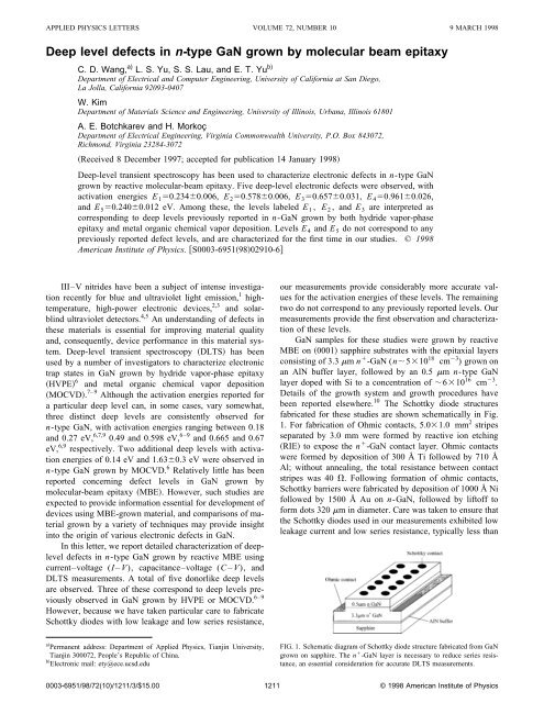
<strong>GaN</strong> samples for these studies were <strong>grown</strong> <strong>by</strong> reactive<br />
MBE on 0001 sapphire substrates with the epitaxial layers<br />
consist<strong>in</strong>g of 3.3 m n -<strong>GaN</strong> (n510 18 cm 3 ) <strong>grown</strong> on<br />
an AlN buffer layer, followed <strong>by</strong> an 0.5 m n-<strong>type</strong> <strong>GaN</strong><br />
layer doped with Si to a concentration of 610 16 cm 3 .<br />
Details of the growth system and growth procedures have<br />
been reported elsewhere. 10 The Schottky diode structures<br />
fabricated for these studies are shown schematically <strong>in</strong> Fig.<br />
1. For fabrication of Ohmic contacts, 5.01.0 mm 2 stripes<br />
separated <strong>by</strong> 3.0 mm were formed <strong>by</strong> reactive ion etch<strong>in</strong>g<br />
RIE to expose the n -<strong>GaN</strong> contact layer. Ohmic contacts<br />
were formed <strong>by</strong> deposition of 300 Å Ti followed <strong>by</strong> 710 Å<br />
Al; without anneal<strong>in</strong>g, the total resistance between contact<br />
stripes was 40 . Follow<strong>in</strong>g formation of ohmic contacts,<br />
Schottky barriers were fabricated <strong>by</strong> deposition of 1000 Å Ni<br />
followed <strong>by</strong> 1500 Å Au on n-<strong>GaN</strong>, followed <strong>by</strong> liftoff to<br />
form dots 320 m <strong>in</strong> diameter. Care was taken to ensure that<br />
the Schottky diodes used <strong>in</strong> our measurements exhibited low<br />
leakage current and low series resistance, typically less than<br />
a Permanent address: Department of Applied Physics, Tianj<strong>in</strong> University,<br />
Tianj<strong>in</strong> 300072, People’s Republic of Ch<strong>in</strong>a.<br />
b Electronic mail: ety@ece.ucsd.edu<br />
FIG. 1. Schematic diagram of Schottky diode structure fabricated from <strong>GaN</strong><br />
<strong>grown</strong> on sapphire. The n -<strong>GaN</strong> layer is necessary to reduce series resistance,<br />
an essential consideration for accurate DLTS measurements.<br />
0003-6951/98/72(10)/1211/3/$15.00 1211<br />
© 1998 American Institute of Physics
1212 Appl. Phys. Lett., Vol. 72, No. 10, 9 March 1998 Wang et al.<br />
FIG. 2. a Forward- and b reverse-bias current–voltage characteristics for<br />
the n-<strong>GaN</strong> Schottky diode structure for temperatures rang<strong>in</strong>g from 100 to<br />
300 K.<br />
100 . This is of considerable importance for accurate<br />
DLTS measurements, as previous studies have shown that<br />
the DLTS peak measured us<strong>in</strong>g a diode with higher series<br />
resistance is shifted toward higher temperature than the peak<br />
measured <strong>in</strong> a diode with lower series resistance for the same<br />
deep <strong>level</strong>. 11<br />
C – V characteristics were measured at frequencies of 10<br />
kHz–1 MHz at temperatures rang<strong>in</strong>g from 90 to 480 K.<br />
Little variation with either temperature or frequency was observed,<br />
and the carrier concentration derived from these measurements<br />
confirmed the dopant concentration of 6<br />
10 16 cm 3 . Figure 2 shows the forward and reverse I – V<br />
characteristics of a Schottky diode for temperatures rang<strong>in</strong>g<br />
from 100 to 300 K. For large forward bias voltages, the I – V<br />
characteristics are dom<strong>in</strong>ated <strong>by</strong> the series resistance of the<br />
Schottky diode. For small bias voltages, the I – V characteristics<br />
are exponential; a detailed analysis of the I – V characteristics<br />
<strong>in</strong> this regime <strong>in</strong>dicates that transport across the<br />
Schottky barrier is heavily <strong>in</strong>fluenced <strong>by</strong> tunnel<strong>in</strong>g. Comb<strong>in</strong>ed<br />
with the carrier concentration derived from C – V measurements,<br />
this suggests that <strong>defects</strong> may play a significant<br />
role <strong>in</strong> transport across the Schottky barrier.<br />
DLTS measurements were performed over a temperature<br />
range of 85–515 K. Typically, a quiescent reverse bias voltage<br />
of 2 V was employed, with fill-pulse voltages rang<strong>in</strong>g<br />
from 1.5 to 2 V. For measurements of deep-<strong>level</strong> concentrations,<br />
a 10 ms pulse was used to <strong>in</strong>sure more complete<br />
fill<strong>in</strong>g of the traps. Rate w<strong>in</strong>dows rang<strong>in</strong>g from 4 to<br />
5000 s 1 were used <strong>in</strong> these measurements. Figure 3 shows<br />
DLTS spectra measured with rate w<strong>in</strong>dows of 1000 and<br />
20 s 1 . A total of five donorlike deep <strong>level</strong>s are observed. In<br />
Fig. 3a, two overlapp<strong>in</strong>g deep-<strong>level</strong> peaks are visible, while<br />
<strong>in</strong> Fig. 3b, peaks correspond<strong>in</strong>g to three deep <strong>level</strong>s are<br />
observed. The peaks labeled E 1 , E 2 , and E 3 correspond to<br />
previously reported deep <strong>level</strong>s <strong>in</strong> n-<strong>GaN</strong>, 6 while E 4 and E 5<br />
are previously unreported <strong>level</strong>s. When the bias voltage, fillpulse<br />
amplitude, and fill-pulse width are varied, the magnitudes<br />
of the DLTS signal peaks and the peak-height ratios<br />
vary, but the temperatures at which peaks are observed rema<strong>in</strong><br />
constant. These observations <strong>in</strong>dicate that the observed<br />
<strong>level</strong>s correspond to bulk <strong>defects</strong>: previous DLTS studies<br />
FIG. 3. a DLTS spectrum measured with an emission rate w<strong>in</strong>dow of<br />
1000 s 1 , a bias voltage of 2 V, fill pulse voltage of 2.0 V, and pulse<br />
width of 10 ms. b DLTS spectrum measured with an emission rate w<strong>in</strong>dow<br />
of 20 s 1 , a bias voltage of 2 V, fill pulse voltage of 1.5 V, and pulse<br />
width of 10 ms.<br />
have shown that bulk <strong>defects</strong> are typically characterized <strong>by</strong><br />
discrete, well-def<strong>in</strong>ed energies while spatially localized <strong>level</strong>s<br />
should exhibit a cont<strong>in</strong>uous distribution <strong>in</strong> energy. 12<br />
Figure 4 shows an Arrhenius plot for all five deep <strong>level</strong>s,<br />
from which we obta<strong>in</strong> the follow<strong>in</strong>g activation energies:<br />
E 1 0.2340.006, E 2 0.5780.006, E 3 0.6570.031,<br />
E 4 0.9610.026, and E 5 0.2400.012 eV. We <strong>in</strong>terpret<br />
the <strong>level</strong> E 1 as correspond<strong>in</strong>g to the defect <strong>level</strong> with activation<br />
energy of 0.264 eV reported <strong>by</strong> Hacke et al. 6 and 0.18<br />
eV reported <strong>by</strong> Götz et al.; 7 the very close correspondence<br />
between the Arrhenius plots for these <strong>level</strong>s and the similar<br />
activation energies derived from these plots suggest that they<br />
correspond to the same defect <strong>level</strong>. Similarly, we <strong>in</strong>terpret<br />
our <strong>level</strong> E 2 as correspond<strong>in</strong>g to the 0.58 eV <strong>level</strong> reported<br />
<strong>by</strong> Hacke et al., 6 the 0.49 eV <strong>level</strong> reported <strong>by</strong> Götz et al. 7<br />
and Lee et al., 8 and the 0.598 eV <strong>level</strong> measured <strong>by</strong> Haase<br />
et al. 9 F<strong>in</strong>ally, our observed <strong>level</strong> E 3 is <strong>in</strong>terpreted as corre-<br />
FIG. 4. Arrhenius plot of emission rate and temperature for the five defect<br />
<strong>level</strong>s detected <strong>by</strong> DLTS. Activation energies are obta<strong>in</strong>ed from the slopes<br />
of the l<strong>in</strong>es correspond<strong>in</strong>g to each <strong>level</strong>.
Appl. Phys. Lett., Vol. 72, No. 10, 9 March 1998<br />
Wang et al.<br />
1213<br />
spond<strong>in</strong>g to the 0.665 eV <strong>level</strong> measured <strong>by</strong> Hacke et al. 6<br />
and the 0.670 eV <strong>level</strong> measured <strong>by</strong> Haase et al. 9 The<br />
Arrhenius plots for the <strong>level</strong>s E 4 and E 5 observed <strong>in</strong> our<br />
measurements differ substantially from those for defect <strong>level</strong>s<br />
reported <strong>in</strong> the literature, <strong>in</strong>dicat<strong>in</strong>g that these correspond<br />
to previously unreported defect <strong>level</strong>s. Our measurements<br />
did not reveal the presence of the 0.14 and 1.630.3 eV<br />
<strong>level</strong>s observed <strong>by</strong> Lee et al. 8 <strong>in</strong> n-<strong>type</strong> <strong>GaN</strong> <strong>grown</strong> <strong>by</strong><br />
MOCVD; the latter, however, would be beyond the range of<br />
activation energies measurable <strong>in</strong> our experiments.<br />
Follow<strong>in</strong>g the procedure of Lang, 13 we can calculate the<br />
concentration of each deep <strong>level</strong>. Assum<strong>in</strong>g that the defect<br />
<strong>level</strong>s are uniformly distributed with<strong>in</strong> the n-<strong>GaN</strong> layer, we<br />
obta<strong>in</strong> the follow<strong>in</strong>g trap concentrations: N 1 7.7<br />
10 14 cm 3 for E 1 ; N 2 1.210 15 cm 3 for E 2 ; N 3<br />
4.210 15 cm 3 for E 3 ; N 4 8.310 15 cm 3 for E 4 ; and<br />
N 5 2.210 14 cm 3 for E 5 .<br />
The exact orig<strong>in</strong> of these deep <strong>level</strong>s rema<strong>in</strong>s an open<br />
question. Haase et al. 9 have suggested that the E 3 <strong>level</strong> may<br />
be associated with a native defect <strong>in</strong> <strong>GaN</strong>: their experiments<br />
demonstrated that this <strong>level</strong> can be generated <strong>in</strong> <strong>GaN</strong> <strong>by</strong> N<br />
implantation and subsequently removed <strong>by</strong> anneal<strong>in</strong>g. In<br />
studies of n-<strong>GaN</strong> <strong>grown</strong> <strong>by</strong> MOCVD, a <strong>level</strong> with activation<br />
energy 0.14 eV and the E 2 <strong>level</strong> were observed <strong>in</strong> <strong>GaN</strong><br />
<strong>grown</strong> us<strong>in</strong>g trimethylgallium TMGa; when TMGa was replaced<br />
<strong>by</strong> triethylgallium TEGa, the 0.14 eV and E 2 <strong>level</strong>s<br />
were no longer detectable <strong>by</strong> DLTS. This was <strong>in</strong>terpreted as<br />
suggest<strong>in</strong>g that the 0.14 eV and E 2 <strong>level</strong>s may be related to<br />
carbon or hydrogen atoms that may be <strong>in</strong>corporated from the<br />
methyl radicals dur<strong>in</strong>g growth. 8 In compar<strong>in</strong>g DLTS measurements<br />
from samples <strong>grown</strong> <strong>by</strong> different techniques, it<br />
would not be unexpected for electronic <strong>level</strong>s aris<strong>in</strong>g from<br />
native <strong>defects</strong> to be observed <strong>in</strong> <strong>GaN</strong> growth <strong>by</strong> a variety of<br />
techniques; conversely, the presence and concentration of defect<br />
<strong>level</strong>s associated with impurities might be expected to<br />
vary <strong>in</strong> material <strong>grown</strong> <strong>by</strong> different techniques.<br />
In summary, we have performed I – V, C – V, and<br />
DLTS characterization of Schottky diodes fabricated from<br />
n-<strong>GaN</strong> <strong>grown</strong> <strong>by</strong> reactive MBE. Particular care was taken to<br />
obta<strong>in</strong> diodes with low series resistance, allow<strong>in</strong>g activation<br />
energies of the electronic defect <strong>level</strong>s observed to be measured<br />
to a high degree of accuracy. DLTS measurements<br />
revealed the presence five electronic deep-<strong>level</strong> <strong>defects</strong> with<br />
activation energies E 1 0.2340.006, E 2 0.5780.006,<br />
E 3 0.6570.031, E 4 0.9610.026, and E 5 0.2400.012<br />
eV. Levels E 1 , E 2 , and E 3 are <strong>in</strong>terpreted as correspond<strong>in</strong>g<br />
to electronic states previously observed <strong>in</strong> <strong>GaN</strong> <strong>grown</strong> <strong>by</strong><br />
HVPE and MOCVD; our measurements represent the first<br />
observation of these <strong>level</strong>s <strong>in</strong> MBE-<strong>grown</strong> <strong>GaN</strong>, and provide<br />
the most accurate measurements to date of the activation<br />
energies for these <strong>level</strong>s. Our measurements have also provided<br />
the first observation and characterization of two additional<br />
<strong>level</strong>s, which we label E 4 and E 5 , <strong>in</strong> <strong>GaN</strong>.<br />
The work at UCSD was supported <strong>by</strong> BMDO Dr. Kepi<br />
Wu monitored <strong>by</strong> USASMDC. W. Kim, A. Botchkarev and<br />
H. Morkoç were funded <strong>by</strong> grants from ONR Dr. C. E. C.<br />
Wood, Dr. Y. S. Park, and M. Yoder and AFOSR Dr. G. L.<br />
Witt. E.T.Y. would like to acknowledge receipt of a Sloan<br />
Research Fellowship.<br />
1 S. Nakamura, M. Senoh, S. Nagahama, N. Iwasa, T. Yamada, T. Matsushita,<br />
H. Kiyoku, and Y. Sugimoto, Jpn. J. Appl. Phys., Part 2, 35, L74<br />
1996.<br />
2 Z. Fan, S. N. Mohammad, O. Aktas, A. E. Botchkarev, A. Salvador, and<br />
H. Morkoç, Appl. Phys. Lett. 69, 1229 1996.<br />
3 Q. Chen, M. A. Khan, J. W. Wang, C. J. Sun, M. S. Shur, and H. Park,<br />
Appl. Phys. Lett. 69, 794 1996.<br />
4 G. Y. Xu, A. Salvador, W. Kim, Z. Fan, C. Lu, H. Tang, H. Morkoç, G.<br />
Smith, and M. Estes, Appl. Phys. Lett. 71, 2154 1997.<br />
5 S. N. Mohammad and H. Morkoç, Prog. Quantum Electron. 20, 361<br />
1996.<br />
6 P. Hacke, T. Detchprohm, K. Hiramatsu, N. Sawaki, K. Tadatomo, and K.<br />
Miyake, J. Appl. Phys. 76, 304 1994.<br />
7 W. Götz, N. M. Johnson, H. Amano, and I. Akasaki, Appl. Phys. Lett. 65,<br />
463 1994.<br />
8 W. I. Lee, T. C. Huang, J. D. Guo, and M. S. Feng, Appl. Phys. Lett. 67,<br />
1721 1995.<br />
9 D. Haase, M. Schmid, W. Kürner, A. Dörnen, V. Härle, F. Scholtz, M.<br />
Burkard, and H. Schwiezer, Appl. Phys. Lett. 69, 2525 1996.<br />
10 W. Kim, Ö. Atkas, A. E. Botchkarev, A. Salvador, S. N. Mohammad, and<br />
H. Morkoç, J. Appl. Phys. 79, 7657 1996.<br />
11 E. V. Astrova, A. A. Lebedev, and A. A. Lebedev, Sov. Phys. Semicond.<br />
19, 850 1985.<br />
12 K. Yamasaki, M. Yoshita, and T. Sugano, Jpn. J. Appl. Phys. 18, 113<br />
1979.<br />
13 D. V. Lang, <strong>in</strong> Topics <strong>in</strong> Applied Physics: Thermally Stimulated Relaxation<br />
<strong>in</strong> Solids, edited <strong>by</strong> P. Bräunlich Spr<strong>in</strong>ger, New York, 1979, p.93.


