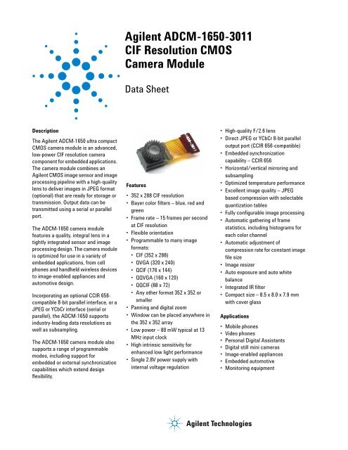
Agilent ADCM-1650-3011 CIF Resolution CMOS Camera Module
Agilent ADCM-1650-3011 CIF Resolution CMOS Camera Module
Agilent ADCM-1650-3011 CIF Resolution CMOS Camera Module

You also want an ePaper? Increase the reach of your titles
YUMPU automatically turns print PDFs into web optimized ePapers that Google loves.
<strong>Agilent</strong> <strong>ADCM</strong>-<strong>1650</strong>-<strong>3011</strong><br />
<strong>CIF</strong> <strong>Resolution</strong> <strong>CMOS</strong><br />
<strong>Camera</strong> <strong>Module</strong><br />
Data Sheet<br />
Description<br />
The <strong>Agilent</strong> <strong>ADCM</strong>-<strong>1650</strong> ultra compact<br />
<strong>CMOS</strong> camera module is an advanced,<br />
low-power <strong>CIF</strong> resolution camera<br />
component for embedded applications.<br />
The camera module combines an<br />
<strong>Agilent</strong> <strong>CMOS</strong> image sensor and image<br />
processing pipeline with a high-quality<br />
lens to deliver images in JPEG format<br />
(optional) that are ready for storage or<br />
transmission. Output data can be<br />
transmitted using a serial or parallel<br />
port.<br />
The <strong>ADCM</strong>-<strong>1650</strong> camera module<br />
features a quality, integral lens in a<br />
tightly integrated sensor and image<br />
processing design. The camera module<br />
is optimized for use in a variety of<br />
embedded applications, from cell<br />
phones and handheld wireless devices<br />
to image-enabled appliances and<br />
automotive design.<br />
Incorporating an optional CCIR 656-<br />
compatible 8-bit parallel interface, or a<br />
JPEG or YCbCr interface (serial or<br />
parallel), the <strong>ADCM</strong>-<strong>1650</strong> supports<br />
industry-leading data resolutions as<br />
well as subsampling.<br />
The <strong>ADCM</strong>-<strong>1650</strong> camera module also<br />
supports a range of programmable<br />
modes, including support for<br />
embedded or external synchronization<br />
capabilities which extend design<br />
flexibility.<br />
Features<br />
• 352 x 288 <strong>CIF</strong> resolution<br />
• Bayer color filters – blue, red and<br />
green<br />
• Frame rate – 15 frames per second<br />
at <strong>CIF</strong> resolution<br />
• Flexible orientation<br />
• Programmable to many image<br />
formats:<br />
• <strong>CIF</strong> (352 x 288)<br />
• QVGA (320 x 240)<br />
• Q<strong>CIF</strong> (176 x 144)<br />
• QQVGA (160 x 120)<br />
• QQ<strong>CIF</strong> (88 x 72)<br />
• Any other format 352 x 352 or<br />
smaller<br />
• Panning and digital zoom<br />
• Window can be placed anywhere in<br />
the 352 x 352 array<br />
• Low power – 80 mW typical at 13<br />
MHz input clock<br />
• High intrinsic sensitivity for<br />
enhanced low light performance<br />
• Single 2.8V power supply with<br />
internal voltage regulation<br />
• High-quality F/2.6 lens<br />
• Direct JPEG or YCbCr 8-bit parallel<br />
output port (CCIR 656-compatible)<br />
• Embedded synchronization<br />
capability – CCIR 656<br />
• Horizontal/vertical mirroring and<br />
subsampling<br />
• Optimized temperature performance<br />
• Excellent image quality – JPEG<br />
based compression with selectable<br />
quantization tables<br />
• Fully configurable image processing<br />
• Automatic gathering of frame<br />
statistics, including histograms for<br />
each color channel<br />
• Automatic adjustment of<br />
compression rate for constant image<br />
file size<br />
• Image resizer<br />
• Auto exposure and auto white<br />
balance<br />
• Integrated IR filter<br />
• Compact size – 8.5 x 8.0 x 7.9 mm<br />
with cover glass<br />
Applications<br />
• Mobile phones<br />
• Video phones<br />
• Personal Digital Assistants<br />
• Digital still mini cameras<br />
• Image-enabled appliances<br />
• Embedded automotive<br />
• Monitoring equipment<br />
<strong>Agilent</strong> Technologies
General Specifications<br />
Feature<br />
Output Format<br />
Maximum Frame Rates<br />
Image Modes<br />
Value<br />
8-bit parallel YCbCr CCIR 656-compliant<br />
8-bit parallel YCbCr or RGB or JPEG<br />
Serial YCbCr or JPEG<br />
15 fps at 352 x 288 (<strong>CIF</strong>)<br />
Grayscale and full color<br />
YCbCr (YUV) Formats 4:4:4 YCbCr and 4:2:2 Y 1 Cb 12 Y 2 Cr 12<br />
Gamma Correction<br />
33 value programmable interpolated table<br />
Data Synchronization<br />
End_of_Line, End_of_Frame, Data_Clock<br />
Video Synchronization<br />
HSYNC, VSYNC, VCLK<br />
Serial Control Identification 0 x 50<br />
Supply Voltage Requirements 2.65 - 3.1 V<br />
External Clock Frequency 4 - 32 MHz<br />
Power Consumption<br />
80 mW typical, 1.5mW in low power mode<br />
Scene Illumination (Minimum) 5 lux<br />
Optical Specifications<br />
Function<br />
Description<br />
Pixel Count<br />
352 x 352 (programmable: 352 x 288 landscape mode; 288 x 352 portrait mode)<br />
Pixel Size<br />
4.9 3m x 4.9 3m<br />
Effective Fill Factor ~ 80%<br />
IR Filter<br />
Integrated<br />
Lens Type<br />
Plastic singlet aspheric<br />
Focal Length<br />
1.85 mm<br />
F/# 2.6<br />
Focus<br />
Fixed focus<br />
Depth of Focus<br />
100 mm to infinity<br />
Field of View<br />
55° full angle (horizontal in landscape mode, vertical in portrait mode)<br />
Distortion ≤ 4%<br />
2
<strong>ADCM</strong>-<strong>1650</strong> <strong>Camera</strong> <strong>Module</strong> Data Sheet<br />
Block Diagram<br />
The <strong>ADCM</strong>-<strong>1650</strong> camera module is a complete image processing system.<br />
Pixel Color<br />
Gain Ratios<br />
Auto White<br />
Balance<br />
CCIR 656<br />
Control<br />
JPEG<br />
Control<br />
Voltage<br />
Regulation<br />
V CC<br />
GND<br />
Sensor<br />
Controller<br />
<strong>Camera</strong><br />
Controller<br />
Auto<br />
Exposure<br />
Test<br />
Generator<br />
Timing Control<br />
Clock –<br />
PLL<br />
MCLK<br />
Pixel Gains<br />
A/D Converter<br />
Pixel<br />
Correction<br />
Demosaic<br />
Color<br />
Balance<br />
Gamma<br />
Correction<br />
Sizer<br />
F2.6<br />
Lens<br />
Pixel<br />
Array<br />
Colorspace<br />
Conversion<br />
RGB<br />
YCbCr<br />
Down<br />
Sampling<br />
YCbCr 4:2:2 Only<br />
JPEG<br />
CCIR 656<br />
OR<br />
Parallel<br />
Data,<br />
Control<br />
D0 -<br />
D7<br />
Window Size<br />
Control<br />
Image<br />
Statistics<br />
Any<br />
Format<br />
OR<br />
Serial<br />
D7<br />
Sensor Config<br />
Registers<br />
Configuration<br />
Registers<br />
Serial Control<br />
Interface<br />
SDATA<br />
SCLK<br />
Image Sensor<br />
Image Processor<br />
<strong>ADCM</strong>-<strong>1650</strong>-<strong>3011</strong> Block Diagram Description<br />
Function<br />
A/D Converter<br />
Auto Exposure<br />
Auto White Balance<br />
<strong>Camera</strong> Controller<br />
CCIR 656 Control<br />
CCIR 656 Output<br />
Clock – PLL<br />
Color Balance<br />
Color Space Conversion<br />
Description<br />
Converts analog pixel output voltages to 8-bit digital values<br />
Adjusts the image sensor exposure for the amount of light present in the window using<br />
both exposure time and pixel gain<br />
Accommodates the slight color shifts that affect white in different kinds of light (daylight,<br />
fluorescent, incandescent). The camera module performs white balancing by digitally<br />
changing the gain ratio of the red, blue and green channels and by adjusting the color<br />
balancing matrix. White objects in the window always look white in the final image.<br />
Overall functions of the camera module are centrally controlled by the camera controller<br />
Determines the logic levels and which type of synchronization codes to use<br />
Accomplished by using the parallel port with CCIR 656 formatted data. Data can be output<br />
with either external horizontal and vertical synchronization signals, or by using embedded<br />
synchronization codes.<br />
Allows very fine control over the system and image sensor clock speeds<br />
Physical properties of the optics dictate that images from the sensor are not perfectly<br />
matched to the human eye. This block improves the color fidelity of the image and<br />
increases saturation.<br />
Programmable color space conversion function to convert RGB values to different color<br />
spaces (default is RGB to YCbCr)<br />
3
<strong>ADCM</strong>-<strong>1650</strong>-<strong>3011</strong> Block Diagram Description (continued)<br />
Function<br />
Configuration Registers<br />
Demosaic<br />
Down-Sampling<br />
Gamma Correction<br />
Sizer<br />
Image Statistics<br />
JPEG Compression<br />
JPEG Control<br />
Lens<br />
Parallel Output<br />
Pixel Array<br />
Pixel Color Gain Ratios<br />
Pixel Correction<br />
Pixel Gain<br />
Sensor Controller<br />
Sensor Configuration<br />
Registers<br />
Serial Control Interface<br />
Test Generator<br />
Timing Control<br />
Voltage Regulation<br />
Window Size Control<br />
Description<br />
Controls all camera module features<br />
Performs color interpolation to produce all three (red, blue and green) color components<br />
for each pixel location<br />
Data is sent in either 4:4:4 mode (no down sampling) or 4:2:2 mode (chrominance down<br />
sampled)<br />
Pixel values acquired from the image sensor are a linear function of the light present in the<br />
frame. For computer monitors, the intensity produced by the display is a non-linear<br />
function of the pixel value and is characterized by a “gamma” curve. The gamma corrects<br />
the image data for display and can also make corrections to the contrast of the image.<br />
Allows the output size of the image to be different than the input size without changing the<br />
field of view. This is done using a sizer circuit which interpolates the new data values from<br />
the image sensor pixels down to smaller images.<br />
Registers contain data for each color plane, are used by the auto exposure and auto white<br />
balance functions and are also readable<br />
Once the image is converted into YCbCr color space, it can then be compressed with<br />
baseline DCT JPEG compression. To reduce the amount of data transmitted, the camera<br />
module does not transmit the JPEG JFIF header, but an index to the Q-table used in the<br />
compression.<br />
Determines the degree of JPEG compression<br />
High quality F/2.6 single element lens<br />
Outputs data using a parallel port with a data clock<br />
Image sensor consists of a 352 x 352 pixel array which can be read in portrait (288 x 352) or<br />
landscape (352 x 288) mode. The array can be windowed to any smaller dimension and can<br />
also be mirrored in both the horizontal and vertical directions.<br />
Controlled by the auto white balance function, these ratios set the differential gains of the<br />
color channels<br />
Reduces the effects of pixel mismatch<br />
Analog gain controlled by the auto exposure block<br />
Controls the interface between the image sensor and the image processor<br />
Controls detailed functions of the image sensor; programming of these registers is done<br />
through four image pipeline registers<br />
<strong>Camera</strong> module registers are programmed using this interface<br />
Generates color bars and other patterns to test the image processor<br />
Exposure control for the image sensor with exposure in row times<br />
Internal voltage regulators<br />
Allows the image sensor output to be windowed to any location on the image sensor.<br />
Beginning and ending rows and columns can be specified, allowing the window to be any<br />
size, in any location.<br />
4
Image Data Flow<br />
<strong>ADCM</strong>-<strong>1650</strong> <strong>Camera</strong> <strong>Module</strong> Data Sheet<br />
The following table shows the flow of data from the sensor, through the image pipeline and out of the camera module.<br />
.<br />
Function Description Settings / Options<br />
Image Data from the Image<br />
Sensor<br />
Auto Exposure<br />
Auto White Balance<br />
Statistics<br />
Pixel Correction<br />
Demosaic<br />
Color Balance<br />
Gamma Correction<br />
Raw data from the image sensor is input<br />
into the image processor<br />
Adjusts image sensor gain and exposure<br />
time to meet target average pixel<br />
luminance<br />
Equalizes average pixel luminance among<br />
color channels<br />
Collects image statistics such as peak<br />
values, pixel sums and histograms on a<br />
one- to-many frame basis<br />
Corrects pixel values for mismatched<br />
pixels<br />
Converts raw Bayer pattern pixel data into<br />
red, green and blue image planes<br />
Adjusts for the color filter response of the<br />
image sensor<br />
Applies a non-linear transfer function to<br />
the image data<br />
Enable/disable using the AEWB_AUTO and<br />
AEWB_STATUS registers<br />
Enable/disable using the STAT_CAP_CNTL<br />
and STAT_MODE_CNTL registers<br />
Enable/disable using the CFG_MAIN2<br />
register<br />
Use default or custom color correction<br />
matrices<br />
Select bottom-weighted or linear lookup<br />
table using the CFG_MAIN1 register; use<br />
default or custom table<br />
Sizer Interpolates the image to a smaller size Select input and output height and width<br />
using the SZR_IN_W, SZR_IN_H,<br />
SZR_OUT_W, SZR_OUT_H registers<br />
Color Space Conversion<br />
Down Sampling<br />
Data Output<br />
Converts RGB data to the desired color<br />
space<br />
Reduces the resolution of the<br />
chrominance data to compress data<br />
Data is output using the CCIR parallel port,<br />
or the serial or parallel port with YCbCr<br />
data or JPEG compression; output is<br />
programmable<br />
Use default (RGB to YCbCr) or custom<br />
conversion matrices<br />
Select down sampling mode (grayscale, 4:4:4<br />
or 4:2:2) using the CFG_MAIN1 register<br />
Select modes using the CCIR_TIMING,<br />
CCIR_CONFIG, Y_MAX, Y_MIN, CbCr_MAX,<br />
CbCr_MIN, CFG_MAIN1 and CFG_MAIN2<br />
registers<br />
5
Electrical Specifications<br />
The descriptions in square brackets are the pin definitions when in JPEG mode. The unbracketed descriptions are for<br />
parallel/CCIR mode,<br />
Absolute Maximum Ratings<br />
Parameter Symbol Minimum Typical Maximum Units Notes<br />
Storage Temperature T S -40 85 °C<br />
Operating Temperature T A -25 65 °C<br />
Humidity RH 5 95 % Non-condensing<br />
Supply Voltage V CC -0.5 3.3 V<br />
ESD 2 kV All pins, human body model<br />
MIL 883 Method 3015<br />
Input Voltage V IN -0.02 3.3 V All input pins<br />
Recommended Operating Conditions<br />
Parameter Symbol Minimum Typical Maximum Units Notes<br />
Operating Temperature T A -25 25 65 °C<br />
V CC Voltage V CC 2.65 2.8 3.15 V<br />
V CC Rise Time V CC_RT 10 ms<br />
V CC Supply Noise V CC_N 50 mV Vp-p within 0 - 1.5 kHz<br />
External Clock Frequency<br />
Duty Cycle<br />
MCLK 4<br />
45<br />
13<br />
50<br />
32<br />
55<br />
MHz<br />
%<br />
Serial Control Clock Frequency SCLK 100 100 kHz Minimum MCLK = 4 MHz<br />
DC Electrical Specifications (typical values at 25 °C, V CC = 2.8 V)<br />
Parameter Symbol Minimum Typical Maximum Units Notes<br />
Supply Current (Normal Mode) I CC 26 mA At 13 MHz<br />
Supply Current (Low Power) I CC 500 3A Power-on, MCLK stopped<br />
Supply Current (Power OFF) I CC 5 3A ON/OFF = OFF<br />
All pins except S_CLK and SDATA<br />
Input Low Voltage V IL 0.6 V<br />
Input High Voltage V IH 1.8 2.8 V<br />
Output Low Voltage V OL 0 0.4 V<br />
Output High Voltage V OH 1.8 V<br />
6
DC Electrical Specifications (typical values at 25 °C, V CC = 2.8 V) (continued)<br />
Parameter Symbol Minimum Typical Maximum Units Notes<br />
Input Low Current I IL < - 5 < 5 3A At 0.0 V<br />
Input High Current I IH < - 5 < 5 3A At 2.5 V<br />
S_CLK and SDATA<br />
Input Low Voltage V IL_S 0.6 V<br />
Input High Voltage V IH_S 2.2 3.6 V<br />
<strong>ADCM</strong>-<strong>1650</strong> <strong>Camera</strong> <strong>Module</strong> Data Sheet<br />
Output Low Voltage V OL_S 0.4 V At 3 mA sink current<br />
Output High Voltage V OH_S V Output voltage depends on<br />
external pull-up resistor and<br />
V CC value<br />
AC Electrical Specifications (typical values at 25 °C, V CC = 2.8 V)<br />
Parameter Symbol Minimum Typical Maximum Units Notes<br />
Video Clock Frequency V CLK 4 13 32 MHz Programmable<br />
Frame Rate 15 frame/s Programmable<br />
ON/OFF Rise Time t OF 40 mV/3s Slew rate<br />
Data Output (DATA_[7:0], VCLK,<br />
HSYNC, VSYNC)<br />
Rise Time t DR 1.9 2.9 4.2 ns V OH = 2.4 V<br />
Fall Time t DF 2.1 3.1 4.3 ns V OH = 2.4 V<br />
S_CLK, S_DATA<br />
Rise Time t DCR ns Depends on external pull-up<br />
resistor, V CC value, line<br />
capacitance<br />
Fall Time t DCF 20 250 ns<br />
Input Pin Capacitance C IN 5.2 pF<br />
7
Pinout<br />
Location Signal Name Type Description Notes<br />
1 GND Common System Ground<br />
2 MCLK Input <strong>Module</strong> Clock<br />
3 VSYNC Output Vertical Synchronization [End_of_Frame]<br />
4 DATA0 Output Parallel Data 0<br />
5 DATA1 Output Parallel Data 1<br />
6 DATA2 Output Parallel Data 2<br />
7 DATA3 Output Parallel Data 3<br />
8 DATA4 Output Parallel Data 4<br />
9 DATA5 Output Parallel Data 5<br />
10 DATA6 Output Parallel Data 6<br />
11 DATA7 Output Parallel Data 7<br />
12 VCLK Output Video Clock [Data_Ready]<br />
13 HSYNC Output Horizontal Synchronization [End_of_Line]<br />
14 ON/OFF Input Voltage Regulator Control<br />
15 SCLK Input Serial Interface Control Clock<br />
16 SDATA Input/Output Serial Interface Control Data<br />
17 V CC Input Voltage Input<br />
18 GND Common System Ground<br />
Pin 1<br />
Mating Connector: Molex 52892-1890<br />
8
Power Up Timing<br />
<strong>ADCM</strong>-<strong>1650</strong> <strong>Camera</strong> <strong>Module</strong> Data Sheet<br />
t MCLK<br />
t SETUP<br />
t VCCOFF<br />
...<br />
V CC<br />
...<br />
...<br />
ON<br />
MCLK<br />
Serial Control<br />
Interface<br />
...<br />
...<br />
...<br />
...<br />
...<br />
Parameter Symbol Minimum Units Notes<br />
V CC to ON ! t ON 0 ms<br />
ON ! to MCLK ON t M_CLK 30 ms<br />
MCLK ON to First Serial Communication t SETUP 2048 Cycles of MCLK<br />
Time from V CC OFF to V CC ON t VCCOFF 600 ms<br />
50<br />
Current Draw vs. MCLK<br />
30<br />
Current Draw vs. Window Size<br />
Current Draw (mA)<br />
40<br />
30<br />
20<br />
Current Draw (mA) @ 13 MHz<br />
25<br />
20<br />
15<br />
10<br />
5<br />
10<br />
4 8 12 16 20 24 28 32<br />
Clock Speed (MHz)<br />
0<br />
<strong>CIF</strong> Q<strong>CIF</strong> QQ<strong>CIF</strong> QVGA QQVGA<br />
Window Size Programmed<br />
9
VCLK Timing<br />
VCLK<br />
Data[7:0]<br />
HSYNC<br />
VSYNC<br />
Data is asserted on the rising edge of VCLK (default) but can be programmed using the camera module registers to be<br />
asserted on the falling edge.<br />
VCLK, HSYNC Timing<br />
MCLK<br />
VCLK<br />
HSYNC<br />
...<br />
...<br />
...<br />
Data[7:0] 00 Y 0<br />
Cb 01<br />
Y 1<br />
Cr 01<br />
Y 2<br />
Cb 23<br />
Y 3<br />
Y N<br />
Cr N-1N<br />
00<br />
First Active Data<br />
...<br />
10
Serial Control Pads Equivalent Circuits<br />
<strong>ADCM</strong>-<strong>1650</strong> <strong>Camera</strong> <strong>Module</strong> Data Sheet<br />
2.8V to 3.3V<br />
ESD<br />
Diode<br />
Stack<br />
I/O Pad Equivalent Circuits<br />
2.8V<br />
1.8V<br />
Pad<br />
Input<br />
Device<br />
I/O Pad<br />
Power Pad<br />
1.8V Shunt<br />
2.8V Shunt<br />
11
<strong>Camera</strong> Orientation<br />
To take pictures “right side up”, orient the camera as shown below. The image can be electronically flipped horizontally,<br />
vertically or both.<br />
Mechanical Drawings<br />
22.63 Ref<br />
8.00<br />
1.35<br />
1.00<br />
4.50<br />
R 5.50<br />
Polyamide<br />
Stiffiner<br />
1.40<br />
4.25<br />
8.50<br />
Pin1<br />
0.90<br />
12.96 Ref<br />
Ø 8.00<br />
5.72<br />
0.046<br />
0.030 5.27<br />
0.030<br />
4.23<br />
6.73<br />
7.68<br />
1.96<br />
0.030<br />
1.20<br />
4.00<br />
1.00<br />
0.70<br />
6.60<br />
0.70<br />
4.25<br />
9.50<br />
8.00<br />
2 - Ø 1.20<br />
1.00<br />
12
Programmable Registers<br />
<strong>ADCM</strong>-<strong>1650</strong> <strong>Camera</strong> <strong>Module</strong> Data Sheet<br />
The <strong>ADCM</strong>-<strong>1650</strong> camera module has programmable registers in the image pipeline IC and the image sensor IC. See “Serial<br />
Control Interface” in the <strong>ADCM</strong>-<strong>1650</strong> <strong>Camera</strong> <strong>Module</strong> Technical Reference Manual for details on usage and programming of<br />
these registers.<br />
Image Pipeline Registers<br />
Mnemonic Description Mnemonic Description<br />
AE_TARGET Auto Exposure Target CC_OFFSET_0 Color Correction Offset 0<br />
AE_TOL Auto Exposure Tolerance CC_OFFSET_1 Color Correction Offset 1<br />
AEWB_AUTO Auto-Exposure/White Balance Function CC_OFFSET_2 Color Correction Offset 2<br />
AEWB_CTRL Auto Functions Control CCIR_CONFIG CCIR Configuration<br />
AEWB_STATUS Auto-Exposure/White Balance Status CCIR_TIMING CCIR Timing Control<br />
APS_COEF_BLUE Blue Color Gain Coefficient CFG_MAIN1 Main Configuration 1<br />
APS_COEF_GRN1 Green 1 Color Gain Coefficient CFG_MAIN2 Main Configuration 2<br />
APS_COEF_GRN2 Green 2 Color Gain Coefficient CSC_COEF_00 Color Space Conversion Coefficient 00<br />
APS_COEF_RED Red Color Gain Coefficient CSC_COEF_01 Color Space Conversion Coefficient 01<br />
APS_DM_CONFIG Sensor Data Mode CSC_COEF_02 Color Space Conversion Coefficient 02<br />
AWB_BLUE_DFLT Default Blue/Green Ratio CSC_COEF_10 Color Space Conversion Coefficient 10<br />
AWB_BLUE_MAX Maximum Blue/Green Ratio CSC_COEF_11 Color Space Conversion Coefficient 11<br />
AWB_BLUE_MIN Minimum Blue/Green Ratio CSC_COEF_12 Color Space Conversion Coefficient 12<br />
AWB_RED_DFLT Default Red/Green Ratio CSC_COEF_20 Color Space Conversion Coefficient 20<br />
AWB_RED_MAX Maximum Red/Green Ratio CSC_COEF_21 Color Space Conversion Coefficient 21<br />
AWB_RED_MIN Minimum Red/Green Ratio CSC_COEF_22 Color Space Conversion Coefficient 22<br />
AWB_TOL Auto White Balance Tolerance CSC_OFFSET_0 Color Space Conversion Offset 0<br />
BLUE_SUM Blue Sum Data CSC_OFFSET_1 Color Space Conversion Offset 1<br />
CbCr_MAX Clip CbCr Values to this Maximum CSC_OFFSET_2 Color Space Conversion Offset 2<br />
CbCr_MIN Clip CbCr Values to this Maximum ETIME_DEFAULT Default Exposure Time<br />
CC_COEF_00 Color Correction Coefficient 00 ETIME_MAX Maximum Exposure Time<br />
CC_COEF_01 Color Correction Coefficient 01 ETIME_MIN Minimum Exposure Time<br />
CC_COEF_02 Color Correction Coefficient 02 EXT_CLK_DIV External Clock Divisor<br />
CC_COEF_10 Color Correction Coefficient 10 G1_G2_THRESH Green Filter Threshold<br />
CC_COEF_11 Color Correction Coefficient 11 GAIN_MAX Maximum Gain<br />
CC_COEF_12 Color Correction Coefficient 12 GAIN_MIN Minimum Gain<br />
CC_COEF_20 Color Correction Coefficient 20 GREEN1_SUM Green 1 Sum Data<br />
CC_COEF_21 Color Correction Coefficient 21 GREEN2_SUM Green 2 Sum Data<br />
CC_COEF_22 Color Correction Coefficient 22 HALF_AC_CYCLE One Half AC Cycle Time Exposure<br />
13
Image Pipeline Registers (continued)<br />
Mnemonic Description Mnemonic Description<br />
I_HEIGHT Current Image Height (Read Only) RESTART JPEG Restart Marker Interval<br />
I_WIDTH Current Image Width (Read Only) REV Revision<br />
NEG_CLIP_CNT Negative Clip Count SENSOR_ADDRESS Sensor Interface Address<br />
OFL_THRESHOLD Auto Q Adjust Overflow Threshold SENSOR_CTRL Sensor Interface Control<br />
ONE_AC_CYCLE One AC Cycle Time Exposure SENSOR_DATA1 Sensor Interface Data Word 1<br />
P_OUTPUT_SPEED Parallel Output Data Speed SENSOR_DATA2 Sensor Interface Data Word 2<br />
PC_BAD_PIX Number of Bad Pixels, Current Frame SER_CTRL_TMG Serial Control Timing<br />
PC_OUTL Pixel Control Outliers SSC_PERIOD Sensor Serial Clock Period<br />
PC_SF_PED Pixel Control Scale Factor, Pedestal STAT_CAP_CTRL Image Statistics Capture Control<br />
PEAK_DATA Peak Sensor Data STAT_MODE_CTRL Image Statistics Mode Control<br />
PLL_CTRL PLL Control STATUS General Image Pipeline Status<br />
PLL_DIVBY PLL Divby Coefficient SZR_IN_H Sizer Input Height<br />
PLL_M PLL M Coefficient SZR_IN_W Sizer Input Width<br />
PLL_PCNT0 PLL P0 Coefficient SZR_OUT_H Sizer Output Height<br />
PLL_PCNT1 PLL P1 Coefficient SZR_OUT_W Sizer Output Width<br />
PLL_QCNT PLL QCNT Coefficient T_DGEN_H Test Data Generator Height (pixels)<br />
PLL_SUM PLL SUM Coefficient T_DGEN_M Test Data Generator Mode Control<br />
POS_CLIP_CNT Positive Clip Count T_DGEN_W Test Data Generator Width (pixels)<br />
Q_TABLE_SELECT Index to JPEG Q-Tables TWO_AC_CYCLES Two AC Cycle Time Exposure<br />
QTABLE_SEL_MAX Maximum Value of QTABLE_SELECT UFL_THRESHOLD Auto Q Adjust Underflow Threshold<br />
QTABLE_SEL_MIN Minimum Value of QTABLE_SELECT Y_MAX Clip Y Values to this Maximum<br />
RED_SUM Red Sum Data Y_MIN Clip Y Values to this Minimum<br />
14
<strong>ADCM</strong>-<strong>1650</strong> <strong>Camera</strong> <strong>Module</strong> Data Sheet<br />
Image Sensor Registers<br />
Mnemonic Description Mnemonic Description<br />
CONFIG Configuration OROCPGA Odd Row, Odd Column PGA Gain<br />
CONFIG_2 Configuration 2 PRST Preset Pulse Width Control<br />
CONTROL Control ROWEXPH Row Exposure High<br />
ERECPGA Even Row, Even Column PGA Gain ROWEXPL Row Exposure Low<br />
EROCPGA Even Row, Odd Column PGA Gain SROWEXP Sub Row Exposure<br />
ERROR Errors STATUS Status<br />
FWCOL First Window Column TCTRL Timing Control<br />
FWROW First Window Row TEST0 Test Control 0<br />
HBLANK Horizontal Blank TEST1 Test Control 1<br />
ICTRL Interface Control TEST2 Test Control 2<br />
IDENT Identification TEST3 Test Control 3<br />
ITMG Interface Timing TEST4 Test Control 4<br />
LWCOL Last Window Column TEST5 Test Control 5<br />
LWROW Last Window Row VBLANK Vertical Blank<br />
ORECPGA<br />
Odd Row, Even Column PGA Gain<br />
15
www.agilent.com/semiconductors<br />
For product information and a complete list of<br />
distributors, please go to our web site.<br />
For technical assistance call:<br />
Americas/Canada: +1 (800) 235-0312 or<br />
+1 (408) 654-8675<br />
Europe: +49 (0) 6441 92460<br />
China: 10800 650 0017<br />
Hong Kong: (+65) 271 2451<br />
India, Australia, New Zealand: (+65) 271 2394<br />
Japan: (+81 3) 3335-8152 (Domestic/International)<br />
or 0120-61-1280 (Domestic Only)<br />
Korea:(+85) 271 2194<br />
Malaysia, Singapore:(+65) 271 2054<br />
Taiwan:(+65) 271 2654<br />
Data subject to change.<br />
Copyright © 2003 <strong>Agilent</strong> Technologies, Inc<br />
May 13, 2003<br />
5988-8934EN<br />
<strong>Agilent</strong> Technologies