Review of Dielectric Resonator Oscillator Technology - IEEE Xplore
Review of Dielectric Resonator Oscillator Technology - IEEE Xplore
Review of Dielectric Resonator Oscillator Technology - IEEE Xplore

You also want an ePaper? Increase the reach of your titles
YUMPU automatically turns print PDFs into web optimized ePapers that Google loves.
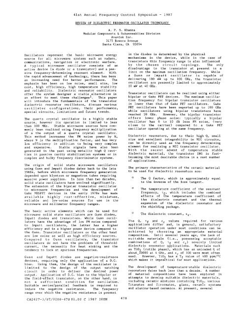
41st Annual Frequency Control Symposium - 1987<br />
REVIEW OF DIELECTRIC RESONATOR OSCILLATOR TECHNOLOGY<br />
A. P. S. Khanna<br />
Modular Components & Subassemblies Division<br />
Avarltek Inc.<br />
3175 Bowers Avenue<br />
Santa Clara, CA 95054<br />
<strong>Oscillator</strong>s represent the basic microwave energy<br />
source for all microwave systems such as radars,<br />
communications, navigation or electronic warfare.<br />
A typical microwave oscillator consists <strong>of</strong> an<br />
active device (a diode or a transistor) and a passive<br />
frequency-determining resonant element. With<br />
the rapid advancement <strong>of</strong> technology, there has been<br />
an increasing need for better performance. The<br />
emphasis has been on low noise, small size, low<br />
cost, high efficiency, high temperature stability<br />
and reliability. <strong>Dielectric</strong> resonator oscillators<br />
<strong>of</strong>fer the system designer a viable alternative in<br />
an effort to meet these challenges'. This paper<br />
will introduce the fundamentals <strong>of</strong> the transistor<br />
dielectric resonator oscillators, discuss various<br />
oscillator configurations, their performance,<br />
special circuits, limitations and future trends.<br />
The quartz crystal oscillator is a highly stable<br />
source, however its operation is limited to less<br />
than 100 MHz. Stable microwave sources have commonly<br />
been realized using frequency multiplication<br />
<strong>of</strong> a the output <strong>of</strong> a quartz crystal oscillator.<br />
This method increases the FM noise power by N,<br />
where N is the multiplication factor, and has very<br />
low efficiency in addition to being very complex<br />
and expensive. Stable signals have also been<br />
generated in the past using metallic high Q cavities<br />
in passive cavity stabilization systems or in<br />
complex and bulky frequency discriminator systems.<br />
The origin <strong>of</strong> solid state microwave oscillators<br />
using Gunn and Impatt diodes dates back to the late<br />
1960s, before which microwave frequency generation<br />
depended upon klystron or magnetron tubes requiring<br />
massive power supplies. In less than two decades,<br />
solid state oscillators have evolved significantly.<br />
The extension <strong>of</strong> the bipolar transistor oscillator<br />
to microwave frequencies and the development <strong>of</strong><br />
GaAs MESFET devices in the early 1970s has made<br />
available highly cost-effective, miniature,<br />
reliable and low-noise sources for use in the<br />
microwave and millimeter frequency ranges.<br />
The basic active elements which can be used for<br />
microwave solid state oscillators are Gunn diodes,<br />
Impatt diodes and transistors. While Gunn oscillators<br />
have the advantage <strong>of</strong> low FM noise compared<br />
to Impatt oscillators, the latter has a higher<br />
efficiency and is a higher power device compared to<br />
the Gunn. Transistor oscillators on the other hand<br />
are low noise as well as high efficiency sources.<br />
Compared to Gunn oscillators, the transistor<br />
oscillators do not have the problems <strong>of</strong> threshold<br />
current, the necessity for heat sinking and the<br />
tendency to lock at spurious frequencies.<br />
Gunn and Impatt diodes are negative-resistance<br />
devices, requiring only the application <strong>of</strong> a D.C.<br />
bias. Using them, the design <strong>of</strong> the oscillator is<br />
limited to the design <strong>of</strong> the output matching<br />
circuit in order to deliver the desired power<br />
output. Application <strong>of</strong> D.C. bias to the bipolar or<br />
the field-effect transistor, on the other hand, is<br />
not a sufficient condition for oscillation.<br />
Suitable series/parallel feedback is required to<br />
induce the negative resistance. The frequency<br />
range over which the negative resistance<br />
present<br />
in the diodes is determined the by physical<br />
mechanisms in the device, while in the case <strong>of</strong><br />
transistors this frequency range is also influenced<br />
by the chosen circuit topology. The only<br />
disadvantage to the transistor at present is a<br />
limit on the maximum oscillation frequency. While<br />
a Gunn or Impatt oscillator is<br />
capable <strong>of</strong><br />
delivering 100 mW up to 100 GHz, the transistor<br />
oscillators are presently limited to approximately<br />
10 mW at 40 GHz.<br />
Transistor oscillators can be realized using either<br />
bipolar or GaAs FET devices. The maximum oscillation<br />
frequency for bipolar transistor oscillators<br />
is lower than that <strong>of</strong> GaAs FET oscillators. GaAs<br />
FET oscillators have been reported up to 100 GHz<br />
while oscillators using bipolar transistors have<br />
reached 20 GHz. However, thebipolartransistor<br />
<strong>of</strong>fers lower phase noise: typically a bipolar<br />
oscillator has 6 to 10 dB less FM noise, (very<br />
close to the carrier) compared to a GaAs FET<br />
oscillator operating at the same frequency.<br />
<strong>Dielectric</strong> resonators, due to their high Q, small<br />
size and excellent integrability in MIC circuits,<br />
can be directly used as the frequency determining<br />
element for realizing a MIC transistor oscillator.<br />
With the recent advent <strong>of</strong> temperature stable<br />
dielectric material, the transistor DRO is fastbecoming<br />
the most desirable choice in vast a number<br />
<strong>of</strong> applications.<br />
The primary characteristics <strong>of</strong> the ceramic material<br />
to be used for dielectric resonators are:<br />
The Q factor, which is approximately equal<br />
to the inverse <strong>of</strong> the loss tangent.<br />
The temperature coefficient <strong>of</strong> the resonant<br />
frequency, ~ f , which includes the combined<br />
effects <strong>of</strong> the temperature coefficient <strong>of</strong><br />
the dielectric constant and the thermal<br />
expansion <strong>of</strong> the dielectric resonator and<br />
the shielding package.<br />
The dielectric constant, cr.<br />
The Q, Tf and cr values required for various<br />
applications differ and, in general, satisfactory<br />
oscillator operation under most conditions can be<br />
achieved by choosing an appropriate material<br />
composition. Until several years ago, the lack <strong>of</strong><br />
suitable materials (i.e., possessing acceptable<br />
combinations <strong>of</strong> Q, Tf and cr) severely limited<br />
dielectric resonator applications. Materials such<br />
as Ti02 (rutile phase). which has an unloaded Q <strong>of</strong><br />
about-10000 at 4 GHz, and cr <strong>of</strong> 100 were most <strong>of</strong>ten<br />
used. However, Ti02 has a Tf value <strong>of</strong> 400 ppm/OC<br />
which makes it impractical for most applications.<br />
The development <strong>of</strong> temperature-stable dielectric<br />
resonators dates back less than a decade. A number<br />
<strong>of</strong> material compositions have been explored in<br />
attempts to develop suitable dielectric materials,<br />
including ceramic mixtures containing Ti02, various<br />
Titanates and Zirconates, glass, ceramic systems<br />
and alumina-based ceramics. At present, several<br />
CH2427-3/87/0000-478$1.00 C 1987 <strong>IEEE</strong> 478
ceramic compositions have been developed <strong>of</strong>fering the dual <strong>of</strong> a metallic cavity. The radiation<br />
excellent dielectric properties. Complex losses <strong>of</strong> the<br />
dielectric resonators with the<br />
perouskite compounds with the general formula A commonly used permittivities, however, are<br />
(B't/3,,By2/3> O3 (where = A Ba, Sr; B'= Zn. Mg, CO, generally much greater than the energy losses in<br />
Ni , B - Ta, Nb) have proved to possess acceptable the metallic cavities, which makes proper shielding<br />
properties for dielectric resonators. These <strong>of</strong> the dielectric resonator a necessity. The<br />
compounds have dielectric constants between 20 and dimensions <strong>of</strong> a dielectric resonator are also<br />
40, a high quality factor, some greater than 10000 considerably smaller than those <strong>of</strong> an empty<br />
@ lOGHz, and a temperature coefficient which is metallic cavity resonant at the same frequency by a<br />
variable through modification <strong>of</strong> the composition. factor <strong>of</strong> approximately l/Er. If is high, the<br />
Table I compares the important Properties Of electric and magnetic fields are confined in region<br />
different materials developed commercially. near the resonator, which results<br />
in small<br />
Ba2 Tig 020 40 10,000 @ 4 GHz<br />
(Z, - Sn) Ti O4 38 10.000 @ 4 GHz<br />
Ba (Zn 113 Ta 2/31 02 30 10,000 @ 10 GHz<br />
Ba (Mg 1/3 Ta 213) 02 25 25,000 @ 10 GHz<br />
Ba 0 - PbO - Nd2 03 - Ti 02 88 5,000 @ 1 GHz<br />
A12 03 11 50,000 @ 10 GHz<br />
TABLE I<br />
DIELECTRIC RESONATOR MATERIALS<br />
DIELECTRIC<br />
TEMPERATURE FREQ .<br />
COMPOSITION CONSTANT P<br />
COEFFICIENT RANGE MANUFACTURER<br />
Whether any <strong>of</strong> the dielectric compositions shown in<br />
Table I have overall superiority is not clear,<br />
since other factors, such as ease <strong>of</strong> ceramic<br />
processing and ability to hold tolerances on the<br />
dielectric properties must also be considered. The<br />
performance limitations, if any, <strong>of</strong> the lower<br />
dielectric constant materials, remain to be<br />
determined, since most component work reported thus<br />
far has used dielectric resonators with cr in the<br />
range <strong>of</strong> 37-100. The lower dielectric constant<br />
material is likely to be<br />
more sensitive to<br />
shielding, due to the increase in fields outside<br />
the resonator.<br />
Resonant Frequency<br />
The resonant frequency <strong>of</strong> a dielectric resonator is<br />
determined both by its dimensions<br />
and its<br />
surroundings. Although the geometrical form <strong>of</strong> a<br />
dielectric resonator is extremely simple, an exact<br />
solution <strong>of</strong> the Maxwell equations is considerably<br />
more difficult than for the hollow metallic cavity.<br />
For this reason, the exact resonant frequency <strong>of</strong> a<br />
certain resonant mode, such as TE016 can only be<br />
computed by rigorous numerical pgocedures. A<br />
number <strong>of</strong> theories on the subject, which can<br />
predict resonant frequency to an accuracy <strong>of</strong> +l%<br />
for the given configuration, appear in the<br />
literature. Unfortunately, these methods call for<br />
the use <strong>of</strong> high-powered computers. Kajfez' has<br />
presented an approximate solution <strong>of</strong> the involved<br />
equations both for the isolated case and for the<br />
more commonly-used MIC configuration. This method<br />
is typically accurate to<br />
9%.<br />
Currently-practical dielectric resonators cover a<br />
frequency range <strong>of</strong> 1 to 100 GHz. The lower<br />
frequency limit is imposed by the resulting large<br />
size <strong>of</strong> the resonator, while the upper frequency is<br />
limited by the reduced Q <strong>of</strong> small resonators, as<br />
well as by dimensions that become too small to<br />
effectively couple with the transmission line.<br />
To a first approximation, a dielectric resonator is<br />
+2 1 To 100 GHz Bell Labs<br />
-4 To 10 Adj 1 To 100 Ghz Trans Tech<br />
Thomson, Murata<br />
0 to 10 4 To 100 Ghz Murata<br />
4 4 To 100 GHz Sumimoto<br />
0 to 6 < 4 GHz Murata/Trans Tech<br />
0 to 6 > 18 GHz? NTK/Trans Tech<br />
radiation losses. The unloaded quality factor Q,<br />
is thus limited by the losses in the dielectric<br />
resonator.<br />
The shape <strong>of</strong> a dielectric resonator is usually a<br />
solid cylinder, but tubular, spherical and<br />
parallelopiped shapes are also used. The commonlyused<br />
resonant mode in cylindrical resonators is<br />
denoted by TEO16. In the TEOIG mode, magnetic<br />
field lines are contained in the meridian plane<br />
while the electric field lines are concentric<br />
circles around z-axis as shown in Fig. 1. For a<br />
distant observer. this mode appears as a magnetic<br />
dipole, and for this reason it is sometimes<br />
referred-to as the "magnetic dipole mode." When<br />
the relative dielectric constant is around 40, more<br />
than 95% <strong>of</strong> the stored electric energy, and more<br />
than 60% <strong>of</strong> the stored magnetic energy, is located<br />
within the cylinder. The remaining energy is<br />
distributed in the air around the resonator,<br />
decaying rapidly<br />
resonator surface.<br />
with distance away from the<br />
To effectively use dielectric resonators in microwave<br />
circuits, it is necessary to have an accurate<br />
knowledge <strong>of</strong> the coupling between the resonator and<br />
different transmission lines. The TE016 mode <strong>of</strong><br />
the cylindrical resonator can he easily coupled to<br />
a microstrip line, fin line, magnetic loop, or to a<br />
metallic or dielectric waveguide1. Figure 2 shows<br />
the magnetic coupling between a dielectric<br />
resonator and microstrip line. The resonator is<br />
placed on top<strong>of</strong>themicrostripsubstrate. The<br />
lateral distance between the resonator and<br />
the<br />
microstrip conductor primarily determines the<br />
amount <strong>of</strong> coupling between the resonator and the<br />
microstrip transmission line2. This has a direct<br />
effect upon output power, frequency stability, and<br />
harmonic content, as well as resonant frequency.<br />
Proper metallic shielding, required to minimize the<br />
radiation losses (hence to increase Q) also affects<br />
the resonant frequency <strong>of</strong> the TE016 mode. Figure 3<br />
shows the equivalent circuit <strong>of</strong> the dielectric<br />
resonator coupled to the line.<br />
479
DRO Circuits and Comparisons<br />
There are two means <strong>of</strong> incorporating a dielectric<br />
resonator in a microstrip circuit: as a passive<br />
stabilization element (stabilized DRO), or as a<br />
circuit element in a frequency determining network<br />
(stable DRO).<br />
A stabilized DRO isadevice which utilizes a<br />
dielectric resonator in the output plane <strong>of</strong> a DRO<br />
circuitry to stabilize an otherwise free running<br />
oscillator (Fig. 4). This approach has several<br />
disadvantages including a tendency toward mode<br />
jumping , frequency hysteresis problems, higher<br />
insertion loss due to the resonator being coupled<br />
to the output circuitry and increased output power<br />
variation.<br />
The stable DRO configuration, which uses the<br />
dielectric resonator as a feedback/frequency<br />
determining element, is the most commonly used,<br />
having greater efficiency, simpler construction and<br />
more resistance to mode jumping and hysteresis<br />
effects than the stabilized DRO.<br />
To realize a stable DRO, the resonator may be used<br />
as either a series or parallel feedback element in<br />
the frequency determining circuit. Figure 5 shows<br />
two common configurations <strong>of</strong> each type'. An<br />
advantage <strong>of</strong> the series feedback design<br />
is the<br />
relative ease <strong>of</strong> coupling to a single line,<br />
compared to the parallel circuit's requirement for<br />
double line coupling. In addition, the two<br />
coupling coefficients in the parallel case are not<br />
independent, increasing the difficulty <strong>of</strong><br />
alignment. With the parallel circuit, however. the<br />
use <strong>of</strong> a high gain amplifier can allow significant<br />
decoupling <strong>of</strong> the resonator from the microstrip<br />
lines, resulting in a higher loaded Q factor with<br />
associated reduction in phase noise.<br />
Electrical Performance Parameters<br />
CenterFrequencyandPowerOutput: As shown in<br />
Figure 6, Transistor DRO's are available spanning<br />
the frequency range <strong>of</strong> 3 GHz to 40 GHz with power<br />
outputs ranging to greater than +25 dBm. As noted<br />
earlier, the oscillator can be either Bipolar or<br />
GasFET, each with associated tradeo<strong>of</strong>sin<br />
performance, and the oscillator can be followed by<br />
one or mroe buffer amplifier stages as required to<br />
meet power output specifications. The center<br />
frequency is usually specified in MHz, to the MHz,<br />
with an associated stability (temperature<br />
dependent) or accuracy (temperature, pulling and<br />
pushing dependant) specification.<br />
Frequency Stability is the measure <strong>of</strong> change in<br />
frequency over the specified operating temperature<br />
range. Typically, this has been expressed in parts<br />
per million per degree centigrade (ppm/OC). As the<br />
actual frequency change versus temperature not is a<br />
linear function about a reference <strong>of</strong> +2S°C, other<br />
methods <strong>of</strong> specifying stability are preferred. One<br />
worthwhile method is to specify a percent change in<br />
frequency over a temperature range, another is to<br />
specify parts per million over<br />
the temperature<br />
range, referred to room temperature.<br />
The principal cause <strong>of</strong> the DRO frequency drift with<br />
temperature the phase deviation between the<br />
resonant circuit and the active circuit, including<br />
device, feedback and output circuitry. Using the<br />
oscillation condition in the reflection coefficient<br />
form, it can be easily proved that the temperature<br />
coefficient <strong>of</strong> DRO frequency is a function <strong>of</strong> the<br />
following parameters:<br />
The temperature coefficient, Tf, <strong>of</strong> the<br />
dielectric resonator placed in a shielded<br />
MIC configuration.<br />
The unloaded Q <strong>of</strong> the dielectric resonator.<br />
The coupling coefficient <strong>of</strong><br />
the microstrip line.<br />
the D.R. with<br />
The temperature coefficient (Tph) <strong>of</strong> the<br />
device (transistor) input reflection<br />
coefficient phase that is known to decrease<br />
linearly with temperature.<br />
In order to achieve a temperature-compensated DRO,<br />
a resonator with a temperature coefficient <strong>of</strong> +l to<br />
+4 ppm/OC is generally required to <strong>of</strong>fset the<br />
negative temperature coefficient <strong>of</strong> the device<br />
phase temperature coefficient. Figure 7 shows some<br />
<strong>of</strong> the typical frequency drift<br />
curves over<br />
temperature for free-running DROs.<br />
With present technology it is now possible to<br />
repeatably produce DROs with frequency drift <strong>of</strong><br />
less than +l00 ppm over the -55 to +85 'C military<br />
temperature range, at frequencies up to 40 GHz.<br />
However, as shown in Fig. 7. results reported in R<br />
& D environment are significantly better (+l0 ppm<br />
over temperature)3.<br />
Certain system applications require higher<br />
temperature stabilities than the ones achievable<br />
using free running DROs. A number <strong>of</strong> techniques<br />
used to improve the temperature stability<br />
are:<br />
The DiRitally Compensated DRO (DC-DRO), in which a<br />
temperature sensor is mounted in the oscillator to<br />
detect the temperature changes. Using EPROMs. preprogrammed<br />
with temperature characteristics <strong>of</strong> the<br />
DRO and a look-up table in the ROM, AID & D/A<br />
convertors provide the necessary correction signal,<br />
which is applied to the varactor bias <strong>of</strong> an<br />
electronically-tuned DRO. Using this technique<br />
frequency stability <strong>of</strong> _f 15 ppm can be obtained<br />
over temperature'.<br />
The Analog-Compensated DRO (AC-DRO), which uses<br />
less-complex circuitry, consisting <strong>of</strong> an analog<br />
compensator circuit in conjunction with<br />
a<br />
temperature sensor, to achieve up to -+20 ppm<br />
frequency stability. Each oscillator is<br />
characterized by generating a custom tuning<br />
voltage-vs.-temperature curve required to maintain<br />
a constant frequency. The compensation circuit is<br />
aligned to fit the tuning voltage vs. temperature<br />
curve <strong>of</strong> the specific oscillator. The correction<br />
voltage from the output circuit is applied to the<br />
tuning varactor <strong>of</strong> the ET-DRO, thus maintaining a<br />
constant frequency'.<br />
Ovenization is also used to enhance the temperature<br />
stability <strong>of</strong> a DRO. To achieve temperature<br />
stability, the oscillator package is inserted in a<br />
temperature-stabilized oven. Using a heater<br />
element, a quick-response thermistor and associated<br />
control circuitry, the package temperature can be<br />
480
maintained within +S OC at 5 to 10 degrees above<br />
the maximum ambient temperature. A total frequency<br />
stability <strong>of</strong> better than +l0 ppm can be obtained<br />
using this approach.<br />
Ovenized DROs <strong>of</strong>fer better phase noise compared to<br />
the AC-DRO and DC-DRO because the DRO does not need<br />
to incorporate electrical tuning circuitry. Analogand<br />
digitally-compensated DROs, however, are<br />
smaller in size and do not need the substantial<br />
amount <strong>of</strong> heater power required by the ovenized<br />
DRO .<br />
Phase Locked DROs (PL-DRO) and Injection Locked<br />
DROs (IL-DRO) are used when the requisite frequency<br />
stability and phase noise cannot be achieved using<br />
the previously-described approaches. A PL-DRO or<br />
IL-DRO approach also becomes necessary when<br />
multiple oscillators are required to be phase or<br />
frequency coherentor both. For locked systems, a<br />
highly stable crystal-controlled signal source<br />
operating at HF or VHF is used as a reference<br />
oscillator.<br />
In injection locking, a VHF power amplifier driving<br />
a step-recovery diode is used to generate a<br />
wideband harmonic comb, which includes the required<br />
locking frequency. A bandpass filter is used to<br />
select the frequency <strong>of</strong> interest, and a freerunning<br />
DRO is locked to the harmonic <strong>of</strong> the<br />
reference source through the injection locking<br />
circuit shown in Fig. 8. The main requirement in<br />
this case is to make sure that the DRO frequency<br />
drift under all operating conditions is less than<br />
the injection locking bandwidth, Af. This<br />
bandwidth is a function <strong>of</strong> the injection power,<br />
oscillator output power, and external Q.<br />
Figure 9 shows a typical phase-locked DRO circuit.<br />
A DC-coupled samplerfphase detector is used to mix<br />
the nearest harmonic <strong>of</strong> the amplified crystal<br />
oscillator with the incoming frequency from the<br />
DRO. If the difference frequency is small enough,<br />
the loop will be driven towards a point where the<br />
difference frequency out <strong>of</strong> the sampler becomes<br />
zero. The loop then drives the DRO towards a zero<br />
phase error condition. A search mechanism is<br />
generally included in the system so that the loop<br />
will be forced to tune through a stable lock point<br />
if the initial difference frequency is too large<br />
for capture to occur. An AC-coupled phase-locked<br />
DRO circuit is used when the output frequency <strong>of</strong><br />
the DRO is not harmonically<br />
related to the<br />
reference oscillator frequency.<br />
Injectionlockingissimplerand less expensive<br />
approach compared to phase locking, but the RF<br />
output is more likely to contain spurious signals<br />
at the harmonics <strong>of</strong> the reference oscillator<br />
frequency. Injection locking, in reality, is<br />
frequency locking as opposed to phase locking.<br />
Single Sideband Phase Noise<br />
Phase noise can be defined as short-term frequency<br />
stability, characterized by frequency variations in<br />
the output frequency which appear as FM energy<br />
around the carrier frequency. Phase noise is<br />
specified in dBcfHz measured at specified <strong>of</strong>fests<br />
from the carrier frequency: typical <strong>of</strong>fsets are 10<br />
and 100 kHz. In a DRO, phase noise is primarily<br />
dependent on four factors:<br />
1. The low frequency noise inherent in the<br />
active device.<br />
2. F,, defined as the upconversion factor, a<br />
measure <strong>of</strong> the efficiency in the conversion<br />
<strong>of</strong> thelowfrequencynoisetothephase<br />
noise <strong>of</strong> the microwave oscillator.<br />
3. The loaded Q factor <strong>of</strong> the dielectric<br />
resonator.<br />
4. The output power (or external Q) <strong>of</strong> the<br />
oscillator.<br />
Optimization <strong>of</strong> phase noise performance calls for<br />
special design considerations, as well as the use<br />
<strong>of</strong> a high-Q dielectric resonator and proper device<br />
selection. It has been proven that the lowfrequency<br />
noise in a GaAs FET is inversely<br />
proportional to the gate length and width <strong>of</strong> the<br />
device. Figure 10 compares the phase noise<br />
performance <strong>of</strong> a number <strong>of</strong> different oscillators.<br />
The following techniques can also<br />
further reduce phase noise:<br />
be used to<br />
Low frequency feedback, using a parallel feedback<br />
circuit designed at low frequencies (up to 1 MHz)<br />
in order to reduce upconversion <strong>of</strong> the low<br />
frequency noise. Phase noise improvement <strong>of</strong> up to<br />
20 dB has been reported using this technique5.<br />
Noise degeneration, using the same dielectric<br />
resonator both as the frequency determining element<br />
<strong>of</strong> the oscillator and the dispersive element <strong>of</strong> the<br />
frequency discriminator. The DC output <strong>of</strong> the<br />
discriminator is applied to the frequency control<br />
point <strong>of</strong> the DRO. This technique has been reported<br />
to achieve phase noise as low as -120 dBc @ 10 KHz<br />
at 10 GHz from the carrier6.<br />
Mechanical Tuning<br />
The frequency <strong>of</strong> oscillation <strong>of</strong> the dielectric<br />
resonator is dependant on a number <strong>of</strong> factors, not<br />
the least <strong>of</strong> which is its proximity to the ground<br />
plane. To take advantage <strong>of</strong> this, a tuning screw<br />
can be installed in the top cover directly above<br />
the resonator which, by reducing the distance<br />
between the resonator and the apparent ground<br />
plane, will provide for a certain amount <strong>of</strong> change<br />
in the resonant frequency (Fig. 11). The reason<br />
for such behavior can be found in the cavity<br />
perturbation theory. Namely, when a metal wall <strong>of</strong> a<br />
resonant cavity is moved inward, the resonant<br />
frequency will decrease if the stored energy is<br />
predominantly in the electric field. Otherwise,<br />
when the stored energy close to the magnetic walls<br />
is mostly magnetic, as is the case for the shielded<br />
TEo~ dielectric resonator considered here, the<br />
resonant frequency will increase when the wall<br />
moves inward. Current designs allow for up to 5<br />
percent tuning range without degradation <strong>of</strong> other<br />
performance parameters. A properly-designed<br />
mechanical tuning option will provide a maximum <strong>of</strong><br />
tuning range while still maintaining hermeticity<br />
and reliability, and will not appreciably affect<br />
the resonator Q factor (apparent as a degradation<br />
in noise and power performance) or temperature<br />
stability.<br />
Electronic Tuning<br />
The YIG-tuned oscillator (YTO) and varactor-tuned<br />
481
oscillator (VCO) are the commonly used<br />
electronically-tunable oscillators. YTO's are<br />
selected for high tuning linearity, large tuning<br />
bandwidth (>2 octaves) and low phase noise. Their<br />
disadvantages are low tuning speed, cumbersome<br />
mechanical size, considerable weight and<br />
significant tuning power consumption. VCO's, on the<br />
other hand, <strong>of</strong>fer small size and weight, high<br />
tuning speed, low tuning power, but have relatively<br />
poor tuning linearity, inferior phase noise and<br />
generally lower bandwidth (< one octave). For some<br />
applications, however, such as FMCW radar sources,<br />
narrowband-modulated communication systems or PLL<br />
systems, bandwidth needs are on the order <strong>of</strong> 0.1 to<br />
1% ; and these applications require sources with<br />
low phase noise, high tuning speed and low tuning<br />
power. Electronically tunable DRO's (ET-DRO) can<br />
now meet the requirements for many <strong>of</strong> these<br />
applications.<br />
ET-DRO's are also commonly used for analog/digital<br />
temperature compensation <strong>of</strong> the oscillator. This<br />
application requires that the frequency tuning <strong>of</strong><br />
the DRO should exceed the frequency drift <strong>of</strong> the<br />
oscillator under any combination <strong>of</strong> operating<br />
conditions (temperature, load and bias variations).<br />
Various means are used to electrically tune the<br />
DRO', including ferrite tuning, optical tuning, and<br />
the more popular varactor and bias tuning.<br />
Varactor tuning (a typical scheme shown in Fig. 12)<br />
can provide up to 1% frequency adjustment. The<br />
dielectric resonator is coupled to another<br />
microstrip line connected to a varactor, resulting<br />
in mutually-coupled resonant circuits. The biasvoltage-dependant<br />
capacitance <strong>of</strong> the varactor<br />
varies the resonant frequency <strong>of</strong> the low-Q resonant<br />
circuit with the tuning voltage. The amount <strong>of</strong><br />
frequency tuning range can be controlled by varying<br />
the coupling between the low-Q<br />
microstripline/varactor circuit and the dielectric<br />
resonator circuit. Tighter coupling permits<br />
greater tuning range, however the attendant<br />
degradation in the Q factor manifests itself<br />
primarily as an increase in phase noise. Varactor<br />
tuning is by far the most<br />
common means <strong>of</strong><br />
incorporating electronic tuning.<br />
Bias voltage tuning takes advantage <strong>of</strong> the<br />
sensitivity to changes in the supply voltage <strong>of</strong> the<br />
device used as an oscillator. By not using an<br />
internal voltage regulator, the oscillator can be<br />
designed to provide the necessary tuning range by<br />
varying the supply voltage, typically within .l% <strong>of</strong><br />
center frequency. As output power is <strong>of</strong>ten a<br />
function <strong>of</strong> supply voltage, care must be exercised<br />
to maintain suitable output power variation<br />
characteristics.<br />
Figure 13 shows the phase noise characteristics for<br />
an electronically-tuned DRO using a varactor. It<br />
may be noted that increase in electrical tuning<br />
results in increased phase noise. Figure 14<br />
reflects the frequency tuning and modulation<br />
sensitivity characteristics with tuning voltage and<br />
also shows the output power fluctuation over the<br />
tuning range. The electrically tunable DROs are<br />
presently available up to 26.5 GHz.<br />
In an optically-tunable dielectric resonator<br />
configuration (Fig. 15), photosensitive material,<br />
such as high-resistivity silicon, is placed<br />
directly on the dielectric resonator. Light from a<br />
laser or light-emitting diode (LED) is brought<br />
through an optical fiber to illuminate the<br />
photosensitive material, changing its conductivity<br />
and perturbing the electromagnetic fields in and<br />
around the resonator. This perturbation results in<br />
a shift in the center frequency <strong>of</strong> the DRO. Using<br />
this technique tuning bandwidths <strong>of</strong> >0.1% can be<br />
obtained.<br />
Special DRO Circuits<br />
Excellent integrability and high performance <strong>of</strong> the<br />
dielectric resonators has generated a large number<br />
<strong>of</strong> interesting DRO configurations for various<br />
system applications. Some <strong>of</strong> those special circuits<br />
will be described in this section:<br />
A dual-resonator oscillator, shown in Fig. 16,<br />
presents a highly stable DRO circuit using<br />
identical resonators in a series feedback<br />
configuration in both the source and gate circuit<br />
<strong>of</strong> a FET7. This oscillator has three output ports,<br />
and its microstrip circuitry is wideband due to the<br />
simple, minimally-tuned 50-ohm lines on all three<br />
ports <strong>of</strong> the transistor. This oscillator is not<br />
particularly susceptible to spurious oscillations,<br />
and can provide high temperature stabilities by<br />
selecting appropriate dielectric mixes for the<br />
resonators.<br />
A push-push DRO (Fig. 17 ) can use a common<br />
dielecric resonator for two transistors. In this<br />
approach the fundamental frequency <strong>of</strong> the<br />
oscillators is cancelled and the second harmonics<br />
are added at the output plane <strong>of</strong> the oscillator.<br />
This circuit helps to generate low-noise<br />
oscillations at frequencies much higher than<br />
otherwise possible. For example, using an 18 GHz<br />
resonator, a GaAs FET DRO was reported to have a<br />
phase noise <strong>of</strong> -100 dBc @ 100KHz8. Figure 18 shows<br />
a comparison <strong>of</strong> phase noise between an Avantek 18<br />
GHz push-push bipolar DRO and fundamental GaAs FET<br />
oscillator.<br />
A selectable multi-frequency oscillator development<br />
appears in Fig. 19 The diagram shows a fastsettling<br />
tri-frequency selectable DRO. A single<br />
GaAs FET is used in conjunction with a simple<br />
single-pole three-throw (SP3T) switch to select the<br />
dielectric resonator corresponding to the desired<br />
output RF frequency. Compared to the old approach<br />
<strong>of</strong> using several continuously-operating DROs and a<br />
high isolation, matched SP3T switch, this approach<br />
is free <strong>of</strong> the spurious signals at the unselected<br />
frequencies. This approach is also less expensive,<br />
uses less number <strong>of</strong> components and is more reliable<br />
compared to the old approach. The output frequency<br />
settles within 210 ppm in less than 2<br />
microseconds9.<br />
A silicon monolithic self-oscillating mixer using a<br />
Darlington pair is shown in Fig. 20. The dielectric<br />
resonator is used in parallel feedback between the<br />
input and output <strong>of</strong> the device. RF input is mixed<br />
with the LO in the first transistor Q1 and the<br />
second transistor <strong>of</strong>fers gain at the IF frequency.<br />
Using this configuration an RF signal at 3.7 to 4.2<br />
GHz was down converted to 1 to 1.5 GHz IF with dB<br />
conversion gain 10.<br />
Limitations <strong>of</strong> Transistor DROs<br />
Free-running DROs presently do not have the low<br />
phase noise and temperature stabilities required<br />
for certain high-performance applications. This<br />
482
limitation necessitates the use <strong>of</strong> phase locking,<br />
injection locking, ovenizing or analog or digital<br />
compensation circuits when necessary. Another<br />
important limitation <strong>of</strong> the DRO is the effect <strong>of</strong><br />
vibration on the performance<strong>of</strong>theDRO.Under<br />
vibration the variation <strong>of</strong> the distance between the<br />
resonatorandtheoutershieldingisthemajor<br />
cause <strong>of</strong> the deterioration <strong>of</strong> the phase noise. A<br />
random vibration density <strong>of</strong> 0.2 G2/Hz can increase<br />
the phase noise by more than 20 dB up to the<br />
highest frequency <strong>of</strong> vibration. Phase locking or<br />
injection locking are typically used to minimize<br />
these effects.<br />
Future Trends<br />
The dielectric resonator oscillator technology is<br />
developing exceedingly rapidly. Emphasis will<br />
continue to develop higher performing DROs.<br />
The<br />
following aspects are likely to be dealt with in<br />
the near future:<br />
Lower phase noise and higher temperature<br />
stability oscillators.<br />
Extension <strong>of</strong> both lower and<br />
frequency coverage.<br />
upper<br />
Higher power at millimeter frequencies<br />
Reduction in cost and size<br />
Wider mechanical and electrical tuning<br />
bandwidths<br />
Improvement in DRO performance under<br />
vibration<br />
Optical tuning & injection locking<br />
Development <strong>of</strong> new materials for<br />
dielectric resonators for linear<br />
temperature coefficient and higher<br />
quality factor.<br />
Use <strong>of</strong> higher-order modes.<br />
REFERENCES:<br />
1.<br />
2.<br />
3.<br />
4.<br />
5.<br />
6.<br />
7.<br />
8.<br />
9.<br />
D. Kajfez and P. Guillon, <strong>Dielectric</strong><br />
<strong>Resonator</strong>s, Artech House 1986.<br />
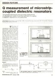
A. P. S. Khanna, "Q measurements <strong>of</strong><br />
microstrip coupled dielectric resonators,"<br />
Microwaves and RF, vol. 23, pp. 81-86, Jan.<br />
1984.<br />
C. Tsironis and V.Pauker,"Temperature<br />
Stabilization <strong>of</strong> GaAs MESFET <strong>Oscillator</strong>s<br />
Using <strong>Dielectric</strong> <strong>Resonator</strong>s," <strong>IEEE</strong> Trans.<br />
MTT., Vol. MTT-31, pp. 312-314, March 1983.<br />
J. Lee et al., "Digital and analog<br />
frequency-temperature compensation <strong>of</strong><br />
dielectric resonator oscillators," <strong>IEEE</strong> MTT-<br />
S Int. Microwave Symposium Digest., pp.277-<br />
279, San Fransisco, 1984.<br />
M. Prigent & J. Obregon, "Phase Noise<br />
Reduction in FET <strong>Oscillator</strong>s by Low-<br />
Freauencv Loading and Feedback Circuitry<br />
Opti&zacion," IEfE Trans. MTT., Vol.MTT-5,<br />
No.3, pp. 349-352, March 1987.<br />
Z. Galani et al., "Analysis and design <strong>of</strong> a<br />
sinele-resonator GaAs FET oscillator with<br />
Y<br />
noise degeneration," <strong>IEEE</strong> Trans. MTT., vol.<br />
MTT-32, pp. 1556-1565. Dec. 1984.<br />
A.P.S. Khanna et al, "Efficient, low noise<br />
three port X-Band FET oscillator using two<br />
dielectric resonators" <strong>IEEE</strong> MTT-S Int.<br />
Microwave Symposium Digest., pp.277-279,<br />
Dallas, 1982.<br />
A.M. Pavio & M.A. Smith,"Push-Push<br />
<strong>Dielectric</strong> <strong>Resonator</strong> <strong>Oscillator</strong>," <strong>IEEE</strong> MTT-S<br />
Int. Microwave Symposium Digest., pp, 266-<br />
269, St. Louis, 1985.<br />
A.P.S. Khanna & R. Soohoo,"Fast Switching X<br />
and Ku Band Multi Frequency <strong>Dielectric</strong><br />
<strong>Resonator</strong> <strong>Oscillator</strong> Using A Single GaAs<br />
FET," <strong>IEEE</strong> MTT-S Int. Microwave Symposium<br />
Digest., pp. 189-191, Las Vegas, 1987.<br />
10.<br />
I. Kipnis & A.P.S. Khanna,"lO GHz Frequency<br />
Convertor Silicon Bipolar "IC," Electronics<br />
Letters 6th Nov. 1986 Vo1.22 No.23 pp. 1270-<br />
1271.<br />
483
SERIES FEEDBACK<br />
Fiq. 1 Field distribution <strong>of</strong> TEOIS mode in a<br />
dielectric resonator.<br />
I<br />
D.?.<br />
I<br />
I c1<br />
fo<br />
-<br />
L<br />
PARRLLEL FEEDBACK<br />
Fiq. 5 Stable Transistor<br />
OR0 Configurations<br />
3a'<br />
Substrate<br />
Mlcrostrip<br />
DR<br />
Fig. 2 <strong>Dielectric</strong> <strong>Resonator</strong> Couoled<br />
blicrostrip line.<br />
I<br />
to a<br />
7<br />
-0<br />
4t<br />
I.<br />
l *\<br />
Free Runn lng GaAs Fo - FET 12 ril CR9<br />
Fig. 3 Eqv. Ckt. <strong>of</strong> 0.R. counled to a microstrip<br />
1 ine.<br />
<strong>Dielectric</strong><br />
<strong>Resonator</strong><br />
2<br />
Fig. 4 Stabilized GaAs FET DRO.<br />
Fig. 7 Frequency Drift vs. Temperature for<br />
typical DROs.<br />
484
&ZVARRCTOR<br />
CRYSTRL<br />
D.E. @<br />
S. R. D<br />
Fig. 8 Injection Locked<br />
ic<br />
DRO<br />
T<br />
-<br />
_I<br />
-<br />
Fig. 12 Varactor Tuned DRO.<br />
-40<br />
-60<br />
-80<br />
-100<br />
L.O.<br />
-120<br />
Fiq. 9 Phase Locked DRO.<br />
-140<br />
-40<br />
-60<br />
,-. -B0<br />
5<br />
% -100<br />
v<br />
-120<br />
J<br />
8 -140<br />
_1<br />
1K 10K 100K 1M<br />
FOURIER FREQUENCY (Hz)<br />
36 GHz<br />
FET<br />
10 GHz<br />
B1 POLRR<br />
.4.0 GHz<br />
B I POLAR<br />
Fig. 10 Phase Noise <strong>of</strong> Transistor DRQs<br />
Fic;. 14. Freq. tuning, modulation sensitivity ti<br />
output power vs. tuning v01 tage for a<br />
VT-DRO.<br />
Fig. 11 Yechanically Tuned DP.0 Confiquration<br />
485
U.R. @<br />
L !<br />
j<br />
l<br />
\<br />
\<br />
Fig. 16 Dual <strong>Dielectric</strong> Eesonator <strong>Oscillator</strong><br />
z<br />
l<br />
Fig. 19 Selectable Multi-freouency<br />
D.R.O.<br />
Fig. 17 Push Dush Transistor DRO.<br />
-4 0<br />
-60<br />
-80<br />
-100<br />
-120<br />
-140<br />
l@K l00K IM<br />
FOURIER FZEQUENCY (Hz)<br />
Fig.<br />
18 Phase Noise Comparison between Push-Push<br />
Bipolar DRO 8 Fundamental GaAs FET DROs.<br />
486