Round LED Module Thermal Management - Universal Lighting ...
Round LED Module Thermal Management - Universal Lighting ...
Round LED Module Thermal Management - Universal Lighting ...

Create successful ePaper yourself
Turn your PDF publications into a flip-book with our unique Google optimized e-Paper software.
Application Note: EVM04<br />
Everline <strong>Module</strong> Application Note:<br />
<strong>Round</strong> <strong>LED</strong> <strong>Module</strong> <strong>Thermal</strong> <strong>Management</strong><br />
PURPOSE:<br />
Use of proper thermal management is a critical element of Light Emitting Diode (<strong>LED</strong>) system<br />
design. The <strong>LED</strong> temperature directly affects device reliability, operation, and compliance with<br />
ULT warranty. As temperatures increase beyond reliability temperature specification limits, the<br />
device lifetime degrades, and above the maximum operating temperature limits severe damage<br />
can occur rendering the <strong>LED</strong> unusable. The purpose of this application note is to provide<br />
system designers with thermal management guidance and tools to implement successful<br />
thermal designs.<br />
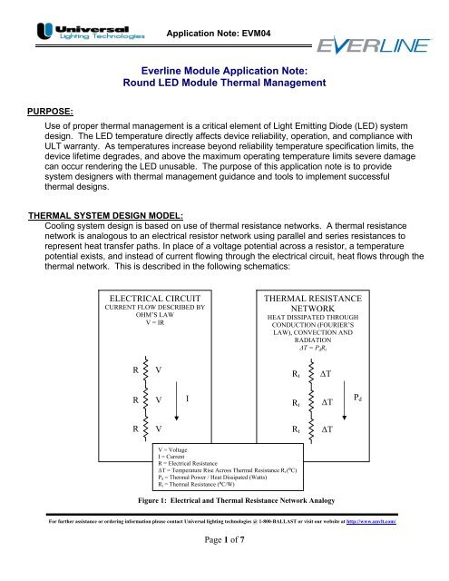
THERMAL SYSTEM DESIGN MODEL:<br />
Cooling system design is based on use of thermal resistance networks. A thermal resistance<br />
network is analogous to an electrical resistor network using parallel and series resistances to<br />
represent heat transfer paths. In place of a voltage potential across a resistor, a temperature<br />
potential exists, and instead of current flowing through the electrical circuit, heat flows through the<br />
thermal network. This is described in the following schematics:<br />
ELECTRICAL CIRCUIT<br />
CURRENT FLOW DESCRIBED BY<br />
OHM’S LAW<br />
V = IR<br />
THERMAL RESISTANCE<br />
NETWORK<br />
HEAT DISSIPATED THROUGH<br />
CONDUCTION (FOURIER’S<br />
LAW), CONVECTION AND<br />
RADIATION<br />
ΔT = P d R t<br />
R<br />
V<br />
R t<br />
ΔT<br />
R<br />
V<br />
I<br />
R t<br />
ΔT<br />
P d<br />
R<br />
V<br />
R t<br />
ΔT<br />
V = Voltage<br />
I = Current<br />
R = Electrical Resistance<br />
ΔT = Temperature Rise Across <strong>Thermal</strong> Resistance R t (⁰C)<br />
P d = <strong>Thermal</strong> Power / Heat Dissipated (Watts)<br />
R t = <strong>Thermal</strong> Resistance (⁰C/W)<br />
Figure 1: Electrical and <strong>Thermal</strong> Resistance Network Analogy<br />
For further assistance or ordering information please contact <strong>Universal</strong> lighting technologies @ 1-800-BALLAST or visit our website at http://www.unvlt.com/<br />
Page 1 of 7
Application Note: EVM04<br />
Design of Cooling System:<br />
This concept of a thermal resistance network model can be used during the system cooling design<br />
phase and during product test after test hardware is available. During the Design Phase, the<br />
Everline® <strong>Round</strong> <strong>Module</strong> solder temperature can be calculated using the networks and<br />
relationships in the following two figures. Employing the appropriate <strong>Module</strong> with Heat Sink<br />
network and equation or the <strong>Module</strong> without Heat Sink network and equation provides a calculated<br />
solder temperature, T s , based on the application average ambient temperature. The calculated T s<br />
can then be compared to the Maximum Reliability Temperature of 85⁰C to determine if the cooling<br />
system design maintains the solder temperature within this temperature specification limit.<br />
<strong>LED</strong> <strong>Module</strong> with Heat Sink:<br />
Network Model:<br />
T a avg<br />
T<br />
∆T la<br />
T hs<br />
T cs T s<br />
hu<br />
R hs<br />
R tim<br />
R s-cs<br />
P d<br />
Model Equation:<br />
T s rel design, hs = T a avg + ∆T hu + P d · (R hs + R tim + R s-cs )<br />
Figure 2: System Design Phase - Network and Equation for <strong>Module</strong> with Heat Sink<br />
where:<br />
T s rel design, hs is the design with heat sink solder temperature for reliability<br />
conditions (⁰C)<br />
T a avg is the average system ambient temperature (⁰C)<br />
∆T hu is the air heat up within the system between T a avg and T la (⁰C)<br />
T la is the temperature of the air near the heat sink (⁰C)<br />
T hs is the heat sink base temperature adjacent to the TIM (⁰C)<br />
T cs is the temperature of the <strong>LED</strong> module adjacent to the TIM (⁰C)<br />
T s is the solder measurement point temperature (⁰C)<br />
P d is the heat dissipated (W)<br />
R hs is the heat sink thermal resistance (⁰C/W)<br />
R tim is the TIM thermal resistance between heat sink and module (⁰C/W)<br />
R s-cs is the thermal resistance from the solder measurement point to the<br />
module case adjacent to the TIM (⁰C/W)<br />
For further assistance or ordering information please contact <strong>Universal</strong> lighting technologies @ 1-800-BALLAST or visit our website at http://www.unvlt.com/<br />
Page 2 of 7
Application Note: EVM04<br />
<strong>LED</strong> <strong>Module</strong> without Heat Sink:<br />
Network Model:<br />
T a avg<br />
∆T hu<br />
T la<br />
T s<br />
R s-la<br />
P d<br />
Model Equation:<br />
T s rel design, no hs<br />
= T a avg<br />
+ ∆T hu<br />
+ P d · R s-la<br />
Figure 3: System Design Phase - Network and Equation for <strong>Module</strong> without Heat Sink<br />
where:<br />
T s rel design, no hs<br />
is the design without heat sink solder temperature for reliability<br />
conditions (⁰C)<br />
T a avg<br />
is the average system ambient temperature (⁰C)<br />
∆T hu<br />
is the air heat up within the system between T a avg<br />
and T la<br />
(⁰C)<br />
T la<br />
is the temperature of the air near the heat sink (⁰C)<br />
T s<br />
is the solder measurement point temperature (⁰C)<br />
P d<br />
is the heat dissipated (W)<br />
R s-la<br />
is the thermal resistance from T s to T la (⁰C/W)<br />
T a avg in the reliability calculation is the average ambient temperature of the <strong>LED</strong> environment to<br />
which the <strong>LED</strong> heat is ultimately dissipated. For example, if the <strong>LED</strong> module is assembled within a<br />
housing, the ambient temperature is that which is external to the housing. This average system<br />
ambient temperature rather than the maximum ambient temperature affects <strong>LED</strong> lifetime.<br />
Both networks include a variable that provides for the air temperature heat up (∆T hu ). Air heat up<br />
can be caused by power supplies, other <strong>LED</strong>’s, or any other heat dissipating devices that affect the<br />
air temperature near the module of interest and cause a temperature rise from the system ambient<br />
air temperature to the module local ambient air temperature. In some cases where no other<br />
devices are present to affect the air temperature this variable contributes 0⁰C to increase in the<br />
solder temperature.<br />
The T la is the temperature of the air near the heat sink at a position that is not affected by heat<br />
convecting from the <strong>LED</strong> or from cooling hardware.<br />
For further assistance or ordering information please contact <strong>Universal</strong> lighting technologies @ 1-800-BALLAST or visit our website at http://www.unvlt.com/<br />
Page 3 of 7
Application Note: EVM04<br />
The location of the solder temperature measurement point, T s , is illustrated in the following figure.<br />
T s<br />
Figure 4: Location of T s<br />
The heat dissipated by the <strong>LED</strong>, P d , is dependent on the efficiency of the <strong>LED</strong>. For design<br />
purposes, the <strong>LED</strong> converts 20% of the input power to light energy and 80% to heat energy.<br />
Consequently, the heat that is dissipated by the cooling system is:<br />
P d = 0.80 · P input = 0.80 · I f · V f<br />
where:<br />
P d is the heat to be dissipated by the system cooling design (W)<br />
P input is the total input power to the <strong>LED</strong> (W)<br />
I f is the forward current through the <strong>LED</strong> (A)<br />
V f is the forward voltage across the <strong>LED</strong> (V)<br />
Heat Sink Selection:<br />
From the above modeling equations, it can be determined if a heat sink is needed to provide<br />
adequate cooling for the <strong>LED</strong> module and what heat sink thermal resistance is required. A<br />
variety of passive and active heat sinks are commercially available from several suppliers.<br />
Common passive heat sinks types used in free or natural convection cooling configurations are:<br />
Extruded, Bonded, Cast, Folded Fin, Forged, Skived, and Stamped. Heat sink performance is a<br />
function of heat sink material thermal conductivity, fin surface area, and fin spacing supporting<br />
air flow between fins. Proper orientation of fins parallel to gravity optimizes flow of air through<br />
the heat sink driven by heated air buoyancy with respect to surrounding cooler air.<br />
For further assistance or ordering information please contact <strong>Universal</strong> lighting technologies @ 1-800-BALLAST or visit our website at http://www.unvlt.com/<br />
Page 4 of 7
Application Note: EVM04<br />
Active heat sink types used in forced convection are: Fan Sinks, Thermoelectric (Peltier)<br />
Devices, Liquid Cooling Systems, Radial Fan Sinks, and Heat Pipes Coupled with Any of these<br />
Heat Sinks.<br />
Additional considerations in selecting either a passive or active heat sink are base thickness<br />
affecting heat spreading that is important to quickly removing heat from the high power density<br />
<strong>LED</strong>’s and base surface flatness and surface roughness needed in conjunction with the TIM<br />
used to avoid air pockets and enhance microscopic contact between heat sink and TIM.<br />
Heat sink supplier performance data can be analyzed to optimize thermal performance for either<br />
heat sink type. Then the thermal performance, cost, weight, size, and reliability (especially for<br />
active heat sinks) will need to be evaluated to determine the best solution for the application.<br />
<strong>Thermal</strong> Interface Material (TIM) Selection:<br />
Again using the above modeling equations, the required thermal performance of a TIM between<br />
the heat sink and <strong>LED</strong> module can be determined. This may require parametric analysis<br />
varying the heat sink and TIM thermal resistance values to establish the required performance<br />
within an achievable range for each.<br />
Several types of TIM are available: Pads, Grease, Gels, Epoxy, Tapes, and Phase Change<br />
Materials. <strong>Thermal</strong> conduction resistance through TIM is the mode of heat transfer.<br />
Consequently, the thickness, thermal conductivity, and coverage area of the TIM controls<br />
thermal performance. A variety of trade-offs are needed to complete the TIM selection and<br />
optimum characteristics can be in conflict between 2 or more of the following. Each needs to be<br />
considered in the selection process:<br />
• High thermal conductivity enhances heat flux<br />
• Minimal thickness reduces thermal resistance<br />
• Maximum area coverage optimizes heat flow<br />
• Conformability to both the <strong>LED</strong> and heat sink surfaces improves conduction of heat<br />
• Increasing heat sink mounting pressure on the TIM generally reduces thermal resistance<br />
• Durability and reworkability if heat sink disassembly and reassembly is required<br />
• Operating temperature range<br />
• Manufacturability/ease of assembly<br />
• Bond line thickness control for liquid TIM’s<br />
• Cost<br />
For further assistance or ordering information please contact <strong>Universal</strong> lighting technologies @ 1-800-BALLAST or visit our website at http://www.unvlt.com/<br />
Page 5 of 7
Application Note: EVM04<br />
COOLING SYSTEM TEST:<br />
ULT has characterized the thermal behavior of the round <strong>LED</strong> module and defined a location for<br />
standardization of the temperature measurement. This measurement location is located near<br />
the center of the module as shown in Figure 4 and is defined as T s . The temperature of the<br />
module at this location must be maintained at or below the value outlined in the specification<br />
sheet, 85⁰C. This requirement has been established to ensure safe operation and stated<br />
lifetimes are achieved.<br />
To determine from measured data if the <strong>LED</strong> is within the temperature specification, the<br />
following relationship can be used to compare the measured thermal performance with the<br />
reliability temperature limit either with or without a heat sink installed. This relationship applies<br />
an adjustment to the measured Ts to compensate for the difference between the average<br />
ambient temperature that is expected for the system and the measured ambient temperature:<br />
T s rel test = T s meas + T a avg spec – T a meas<br />
where:<br />
T s rel test<br />
is the ambient adjusted <strong>LED</strong> module solder temperature for<br />
reliability conditions (⁰C)<br />
T s meas<br />
is the measured <strong>LED</strong> temperature at the location in Figure 4 (⁰C)<br />
T a avg spec<br />
is the expected average system ambient temperature (⁰C)<br />
T a meas<br />
is the measured system ambient temperature (⁰C)<br />
The testing environment of the <strong>LED</strong> module and cooling system should simulate the application<br />
environment as closely as possible. Air movement, power input, ambient temperature,<br />
mechanical orientation, and other heat sources affecting the thermal performance of the <strong>LED</strong><br />
module need to be realistic.<br />
The thermal environment for the typical application of linear <strong>LED</strong> modules does not have<br />
guaranteed air movement in natural convection. Consequently, it is not recommended that<br />
testing be performed in a thermal chamber or oven that uses forced convection or has any<br />
significant air movement within it. Also, natural convection requires significant space to avoid<br />
restriction of natural air movement. The module and cooling system location within the test<br />
environment must have open area surrounding it and quiescent air.<br />
Test multiple <strong>LED</strong>’s and ensure that the <strong>LED</strong> with the expected highest temperature is<br />
measured.<br />
Test until the measured temperatures stabilize at maximum values reaching steady state<br />
temperatures.<br />
For further assistance or ordering information please contact <strong>Universal</strong> lighting technologies @ 1-800-BALLAST or visit our website at http://www.unvlt.com/<br />
Page 6 of 7
Application Note: EVM04<br />
Test with the thermal probe installed at the T s location specified in Figure 4 with direct contact to<br />
the module and secured with thermal epoxy or the equivalent.<br />
Measure T ambient to determine any difference between it and the specified ambient temperature<br />
upper limit.<br />
Use the above test relationship and the measured data from realistic test conditions to<br />
determine if the <strong>LED</strong> module temperature in the system application is within the specified upper<br />
temperature limit.<br />
For further assistance or ordering information please contact <strong>Universal</strong> lighting technologies @ 1-800-BALLAST or visit our website at http://www.unvlt.com/<br />
Page 7 of 7