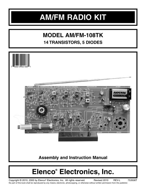
AM/FM RADIO KIT MODEL AM/FM-108TK 14 ... - Elenco
AM/FM RADIO KIT MODEL AM/FM-108TK 14 ... - Elenco
AM/FM RADIO KIT MODEL AM/FM-108TK 14 ... - Elenco

Create successful ePaper yourself
Turn your PDF publications into a flip-book with our unique Google optimized e-Paper software.
<strong>AM</strong>/<strong>FM</strong> <strong>RADIO</strong> <strong>KIT</strong><br />
<strong>MODEL</strong> <strong>AM</strong>/<strong>FM</strong>-<strong>108TK</strong><br />
<strong>14</strong> TRANSISTORS, 5 DIODES<br />
Assembly and Instruction Manual<br />
<strong>Elenco</strong> ®<br />
Electronics, Inc.<br />
Copyright © 2010, 2000 by <strong>Elenco</strong> ® Electronics, Inc. All rights reserved. Revised 2010 REV-L 753508T<br />
No part of this book shall be reproduced by any means; electronic, photocopying, or otherwise without written permission from the publisher.
The <strong>AM</strong>/<strong>FM</strong> Radio project is divided into two parts, the <strong>AM</strong> Radio Section and the <strong>FM</strong> Radio Section. At this time, only<br />
identify the parts that you will need for the <strong>AM</strong> radio as listed below. DO NOT OPEN the bags listed for the <strong>FM</strong> radio. A<br />
separate parts list will be shown for the <strong>FM</strong> radio after you have completed the <strong>AM</strong> radio.<br />
PARTS LIST FOR THE <strong>AM</strong> <strong>RADIO</strong> SECTION<br />
If you are a student, and any parts are missing or damaged, please see instructor or bookstore. If you purchased this kit<br />
from a distributor, catalog, etc., please contact <strong>Elenco</strong> ® Electronics (address/phone/e-mail is at the back of this manual) for<br />
additional assistance, if needed. DO NOT contact your place of purchase as they will not be able to help you.<br />
RESISTORS<br />
Qty. Symbol Value Color Code Part #<br />
r 1 R46 47Ω 5% 1/4W yellow-violet-black-gold 124700<br />
r 4 R38, 43, 48, 49 100Ω 5% 1/4W brown-black-brown-gold 131000<br />
r 1 R47 330Ω 5% 1/4W orange-orange-brown-gold 133300<br />
r 1 R41 470Ω 5% 1/4W yellow-violet-brown-gold 134700<br />
r 1 R37 1kΩ 5% 1/4W brown-black-red-gold <strong>14</strong>1000<br />
r 1 R42 2.2kΩ 5% 1/4W red-red-red-gold <strong>14</strong>2200<br />
r 3 R33, 36, 44 3.3kΩ 5% 1/4W orange-orange-red-gold <strong>14</strong>3300<br />
r 1 R40 10kΩ 5% 1/4W brown-black-orange-gold 151000<br />
r 1 R32 12kΩ 5% 1/4W brown-red-orange-gold 151200<br />
r 1 R35 27kΩ 5% 1/4W red-violet-orange-gold 152700<br />
r 1 R39 39kΩ 5% 1/4W orange-white-orange-gold 153900<br />
r 1 R31 56kΩ 5% 1/4W green-blue-orange-gold 155600<br />
r 1 R45 470kΩ 5% 1/4W yellow-violet-yellow-gold 164700<br />
r 1 R34 1MΩ 5% 1/4W brown-black-green-gold 171000<br />
r 1 Volume/S2 50kΩ / SW Pot/SW with nut and washer 192522<br />
CAPACITORS<br />
Qty. Symbol Value Description Part #<br />
r 1 C30 150pF Discap (151) 221510<br />
r 1 C44 .001μF Discap (102) 231036<br />
r 2 C31, 38 .01μF Discap (103) 241031<br />
r 5 C29, 33, 35, 36, 37 .02μF or .022μF Discap (203) or (223) 242010<br />
r 1 C28 .1μF Discap (104) 251010<br />
r 3 C32, 40, 41 10μF Electrolytic Radial (Lytic) 271045<br />
r 1 C42 47μF Electrolytic Radial (Lytic) 274744<br />
r 1 C34 100μF Electrolytic Radial (Lytic) 281044<br />
r 2 C39, 43 470μF Electrolytic Radial (Lytic) 284744<br />
r 1 C1 Variable Tuning Gang <strong>AM</strong>/<strong>FM</strong> 299904<br />
SEMICONDUCTORS<br />
Qty. Symbol Value Description Part #<br />
r 2 D4, 5 1N4<strong>14</strong>8 Diode 3<strong>14</strong><strong>14</strong>8<br />
r 5 Q7, 8, 9, 10, 11 2N3904 Transistor NPN 323904<br />
r 1 Q12 2N3906 Transistor PNP 323906<br />
r 1 Q<strong>14</strong> MPS8050 or 6560 Transistor NPN 328050<br />
r 1 Q13 MPS8550 or 6562 Transistor PNP 328550<br />
COILS MAGIC WAND<br />
Qty. Symbol Color Description Part # Qty. Description Part #<br />
r 1 L5 Red <strong>AM</strong> Oscillator 430057 r 1 Iron Core 461000<br />
r 1 T6 Yellow <strong>AM</strong> IF 430260 r 1 Brass Core 661150<br />
r 1 T7 White <strong>AM</strong> IF 430262 r 4” Shrink Tubing 890120<br />
r 1 T8 Black <strong>AM</strong> IF 430264<br />
r 1 L4 <strong>AM</strong> Antenna with Holders 484004<br />
Qty. Description Part #<br />
r 1 PC Board 517054<br />
r 1 Switch 541023<br />
r 1 Battery Holder 590096<br />
r 1 Speaker 590102<br />
r 1 Knob (dial) 622040<br />
r 1 Knob (pot) 622050<br />
r 1 Earphone Jack with Nut 622130 or 622131<br />
r 1 Radio Stand 626100<br />
r 1 Earphone 629250<br />
r 1 Screw M2.5 x 7.5mm (dial) 641107<br />
MISCELLANEOUS<br />
**** SAVE THE BOX THAT THIS <strong>KIT</strong> C<strong>AM</strong>E IN. IT WILL BE USED ON PAGES 24 & 53. ****<br />
-1-<br />
Qty. Description Part #<br />
r 3 Screw M1.8 x 7.5mm (battery holder) 641100<br />
r 2 Screw M2.5 x 3.8mm (gang) 641310<br />
r 3 Nut M1.8 644210<br />
r 1 Plastic Washer 645108<br />
r 8 Test Point Pin 665008<br />
r 1 Label <strong>AM</strong>/<strong>FM</strong> 723059<br />
r 1 Speaker Pad 780128<br />
r 8” Wire 22AWG insulated 8<strong>14</strong>520<br />
r 1 Solder Lead-Free 9LF99
IDENTIFYING RESISTOR VALUES<br />
Use the following information as a guide in properly identifying the value of resistors.<br />
BAND 1<br />
1st Digit<br />
Color Digit<br />
Black 0<br />
Brown 1<br />
Red 2<br />
Orange 3<br />
Yellow 4<br />
Green 5<br />
Blue 6<br />
Violet 7<br />
Gray 8<br />
White 9<br />
BAND 2<br />
2nd Digit<br />
Color Digit<br />
Black 0<br />
Brown 1<br />
Red 2<br />
Orange 3<br />
Yellow 4<br />
Green 5<br />
Blue 6<br />
Violet 7<br />
Gray 8<br />
White 9<br />
IDENTIFYING CAPACITOR VALUES<br />
METRIC UNITS AND CONVERSIONS<br />
Abbreviation Means Multiply Unit By Or<br />
p Pico .000000000001 10 -12<br />
n nano .000000001 10 -9<br />
μ micro .000001 10 -6<br />
m milli .001 10 -3<br />
– unit 1 10 0<br />
k kilo 1,000 10 3<br />
M mega 1,000,000 10 6<br />
-2-<br />
BANDS<br />
Capacitors will be identified by their capacitance value in pF (picofarads), nF (nanofarads), or μF (microfarads).<br />
Most capacitors will have their actual value printed on them. Some capacitors may have their value printed in<br />
the following manner. The maximum operating voltage may also be printed on the capacitor.<br />
Electrolytic capacitors have a positive<br />
and a negative electrode. The<br />
negative lead is indicated on the<br />
packaging by a stripe with minus<br />
signs and possibly arrowheads.<br />
Warning:<br />
If the capacitor<br />
is connected<br />
with incorrect<br />
polarity, it may<br />
heat up and<br />
either leak, or<br />
cause the<br />
capacitor to<br />
explode.<br />
Polarity<br />
Marking<br />
Multiplier<br />
Color Multiplier<br />
Black 1<br />
Brown 10<br />
Red 100<br />
Orange 1,000<br />
Yellow 10,000<br />
Green 100,000<br />
Blue 1,000,000<br />
Silver 0.01<br />
Gold 0.1<br />
Multiplier<br />
Second Digit<br />
First Digit<br />
Resistance<br />
Tolerance<br />
Color Tolerance<br />
Silver ±10%<br />
Gold ±5%<br />
Brown ±1%<br />
Red ±2%<br />
Orange ±3%<br />
Green ±0.5%<br />
Blue ±0.25%<br />
Violet ±0.1%<br />
103K<br />
100V<br />
Multiplier<br />
Tolerance*<br />
The value is 10 x 1,000 =<br />
10,000pF or .01μF 100V<br />
Maximum Working Voltage<br />
* The letter M indicates a tolerance of +20%<br />
The letter K indicates a tolerance of +10%<br />
The letter J indicates a tolerance of +5%<br />
1 2 Multiplier Tolerance<br />
For the No. 0 1 2 3 4 5 8 9<br />
Multiply By 1 10 100 1k 10k 100k .01 0.1<br />
Note: The letter “R”<br />
may be used at times<br />
to signify a decimal<br />
point; as in 3R3 = 3.3<br />
1. 1,000 pico units = 1 nano unit<br />
2. 1,000 nano units = 1 micro unit<br />
3. 1,000 micro units = 1 milli unit<br />
4. 1,000 milli units = 1 unit<br />
5. 1,000 units = 1 kilo unit<br />
6. 1,000 kilo units = 1 mega unit
INTRODUCTION<br />
The <strong>Elenco</strong> ® Superhet 108T <strong>AM</strong>/<strong>FM</strong> Radio Kit is a<br />
“superheterodyne” receiver of the standard <strong>AM</strong> (amplitude<br />
modulation) and <strong>FM</strong> (frequency modulation) broadcast<br />
frequencies. The unique design of the Superhet 108<br />
allows you to place the parts over their corresponding<br />
symbol in the schematic drawing on the surface of the<br />
printed circuit board during assembly. This technique<br />
maximizes the learning process while keeping the<br />
chances of an assembly error at a minimum. It is very<br />
important, however, that good soldering practices are<br />
used to prevent bad connections. The Soldering Guide<br />
should be reviewed before any soldering is attempted.<br />
The actual assembly is broken down into 9 sections. The<br />
theory of operation for each section, or stage, should be<br />
GENERAL DISCUSSION<br />
<strong>FM</strong> RF<br />
<strong>AM</strong>PLIFIER<br />
Section 9<br />
<strong>FM</strong><br />
OSCILLATOR<br />
<strong>AM</strong> MIXER<br />
<strong>AM</strong><br />
OSCILLATOR<br />
<strong>FM</strong> MIXER<br />
AFC<br />
Section 8 Section 7 Section 6<br />
1ST <strong>FM</strong> IF<br />
<strong>AM</strong>PLIFIER<br />
1ST <strong>AM</strong> IF<br />
<strong>AM</strong>PLIFIER<br />
2ND <strong>FM</strong> IF<br />
<strong>AM</strong>PLIFIER<br />
Section 5 Section 4 Section 3 Section 2<br />
The purpose of section 1, the Audio Amplifier Stage, is to<br />
increase the power of the audio signal received from the<br />
detector to a power level capable of driving the speaker.<br />
Section 2 includes the <strong>AM</strong> detector circuit and the AGC<br />
(automatic gain control) circuit. The <strong>AM</strong> detector converts<br />
the amplitude modulated IF (intermediate frequency)<br />
signal to a low level audio signal. The AGC stage feeds<br />
back a DC voltage to the first <strong>AM</strong> IF amplifier in order to<br />
maintain a near constant level of audio at the detector.<br />
Section 3 is the second <strong>AM</strong> IF amplifier. The second <strong>AM</strong><br />
IF amplifier is tuned to 455kHz (Kilohertz) and has a fixed<br />
gain at this frequency of 50. Section 4 is the first <strong>AM</strong> IF 2<br />
amplifier which has a variable gain that depends on the<br />
AGC voltage received from the AGC stage. The first <strong>AM</strong><br />
IF amplifier is also tuned to 455kHz. Section 5 includes<br />
the <strong>AM</strong> mixer, <strong>AM</strong> oscillator and <strong>AM</strong> antenna stages.<br />
When the radio wave passes through the antenna, it<br />
induces a small voltage across the antenna coil. This<br />
voltage is coupled to the mixer, or converter, stage to be<br />
changed to a frequency of 455kHz. This change is<br />
accomplished by mixing (heterodyning) the radio<br />
<strong>FM</strong> <strong>RADIO</strong><br />
2ND <strong>AM</strong> IF<br />
<strong>AM</strong>PLIFIER<br />
<strong>AM</strong> <strong>RADIO</strong><br />
-3-<br />
read before the assembly is started. This will provide the<br />
student with an understanding of what that stage has been<br />
designed to accomplish, and how it actually works. After<br />
each assembly, you will be instructed to make certain tests<br />
and measurements to prove that each section is<br />
functioning properly. If a test fails to produce the proper<br />
results, a troubleshooting guide is provided to help you<br />
correct the problem. If test equipment is available, further<br />
measurements and calculations are demonstrated to<br />
allow each student to verify that each stage meets the<br />
engineering specifications. After all of the stages have<br />
been built and tested, a final alignment procedure is<br />
provided to peak the performance of the receiver and<br />
maximize the Superhet 108T’s reception capabilities.<br />
<strong>FM</strong><br />
DETECTOR<br />
<strong>AM</strong><br />
DETECTOR<br />
AFC<br />
Figure 1<br />
AUDIO<br />
<strong>AM</strong>PLIFIER<br />
Section 1<br />
Speaker<br />
frequency signal with the oscillator signal. Section 6 is the<br />
<strong>FM</strong> ratio detector circuit. The <strong>FM</strong> ratio detector has a fixed<br />
gain of about 20. Section 7 is the second <strong>FM</strong> IF amplifier.<br />
The second <strong>FM</strong> IF amplifier is tuned to 10.7MHz<br />
(Megahertz) and has a set gain of approximately 20. The<br />
3dB bandwidth of this stage should be approximately<br />
350kHz. Section 8 is the first <strong>FM</strong> IF amplifier. The first <strong>FM</strong><br />
IF amplifier is also tuned to 10.7MHz and has a set gain of<br />
approximately 10. It also has a 3dB bandwidth of 350kHz.<br />
Section 9 includes the <strong>FM</strong> mixer, <strong>FM</strong> oscillator, <strong>FM</strong> RF and<br />
the AFC circuits. The incoming radio waves are amplified<br />
by the <strong>FM</strong> RF amplifier, which is tuned to a desired radio<br />
station in the <strong>FM</strong> frequency bandwidth of 88MHz to<br />
108MHz. These amplified signals are then coupled to the<br />
<strong>FM</strong> mixer stage to be changed to a frequency of 10.7MHz.<br />
This change, as in <strong>AM</strong>, is accomplished by heterodyning<br />
the radio frequency signal with the oscillator signal. The<br />
AFC stage feeds back a DC voltage to the <strong>FM</strong> oscillator to<br />
prevent the oscillator from drifting. Each of these blocks<br />
will be explained in detail in the Theory of Operation given<br />
before the assembly instructions for that stage.
CONSTRUCTION<br />
Introduction<br />
The most important factor in assembling your Superhet 108 <strong>AM</strong>/<strong>FM</strong><br />
Transistor Radio Kit is good soldering techniques. Using the proper<br />
soldering iron is of prime importance. A small pencil type soldering iron<br />
of 25 - 40 watts is recommended. The tip of the iron must be kept<br />
clean at all times and well-tinned.<br />
Solder<br />
For many years leaded solder was the most common type of solder<br />
used by the electronics industry, but it is now being replaced by leadfree<br />
solder for health reasons. This kit contains lead-free solder, which<br />
contains 99.3% tin, 0.7% copper, and has a rosin-flux core.<br />
Lead-free solder is different from lead solder: It has a higher melting<br />
point than lead solder, so you need higher temperature for the solder to<br />
flow properly. Recommended tip temperature is approximately 700OF; higher temperatures improve solder flow but accelerate tip decay. An<br />
increase in soldering time may be required to achieve good results.<br />
Soldering iron tips wear out faster since lead-free solders are more<br />
corrosive and the higher soldering temperatures accelerate corrosion,<br />
so proper tip care is important. The solder joint finish will look slightly<br />
duller with lead-free solders.<br />
Use these procedures to increase the life of your soldering iron tip when<br />
using lead-free solder:<br />
Keep the iron tinned at all times.<br />
Use the correct tip size for best heat transfer. The conical tip is the<br />
most commonly used.<br />
What Good Soldering Looks Like<br />
A good solder connection should be bright, shiny, smooth, and uniformly<br />
flowed over all surfaces.<br />
1. Solder all components from the<br />
copper foil side only. Push the<br />
soldering iron tip against both the<br />
lead and the circuit board foil.<br />
2. Apply a small amount of solder to<br />
the iron tip. This allows the heat to<br />
leave the iron and onto the foil.<br />
Immediately apply solder to the<br />
opposite side of the connection,<br />
away from the iron. Allow the<br />
heated component and the circuit<br />
foil to melt the solder.<br />
3. Allow the solder to flow around<br />
the connection. Then, remove<br />
the solder and the iron and let the<br />
connection cool. The solder<br />
should have flowed smoothly and<br />
not lump around the wire lead.<br />
4. Here is what a good solder<br />
connection looks like.<br />
Component Lead<br />
Foil<br />
Solder<br />
Foil<br />
Solder<br />
Foil<br />
Soldering Iron<br />
Circuit Board<br />
Soldering Iron<br />
Soldering Iron<br />
-4-<br />
Turn off iron when not in use or reduce temperature setting when<br />
using a soldering station.<br />
Tips should be cleaned frequently to remove oxidation before it becomes<br />
impossible to remove. Use Dry Tip Cleaner (<strong>Elenco</strong> ® #SH-1025) or Tip<br />
Cleaner (<strong>Elenco</strong> ® #TTC1). If you use a sponge to clean your tip, then use<br />
distilled water (tap water has impurities that accelerate corrosion).<br />
Safety Procedures<br />
Always wear safety glasses or safety goggles to<br />
'<br />
protect your eyes when working with tools or<br />
soldering iron, and during all phases of testing.<br />
Be sure there is adequate ventilation when soldering.<br />
Locate soldering iron in an area where you do not have to go around<br />
it or reach over it. Keep it in a safe area away from the reach of<br />
children.<br />
Do not hold solder in your mouth. Solder is a toxic substance.<br />
Wash hands thoroughly after handling solder.<br />
Assemble Components<br />
In all of the following assembly steps, the components must be installed<br />
on the top side of the PC board unless otherwise indicated. The top<br />
legend shows where each component goes. The leads pass through the<br />
corresponding holes in the board and are soldered on the foil side.<br />
Use only rosin core solder.<br />
DO NOT USE ACID CORE SOLDER!<br />
Types of Poor Soldering Connections<br />
1. Insufficient heat - the solder will<br />
not flow onto the lead as shown.<br />
2. Insufficient solder - let the<br />
solder flow over the connection<br />
until it is covered.<br />
Use just enough solder to cover<br />
the connection.<br />
3. Excessive solder - could make<br />
connections that you did not<br />
intend to between adjacent foil<br />
areas or terminals.<br />
4. Solder bridges - occur when<br />
solder runs between circuit paths<br />
and creates a short circuit. This is<br />
usually caused by using too much<br />
solder.<br />
To correct this, simply drag your<br />
soldering iron across the solder<br />
bridge as shown.<br />
Solder<br />
Rosin<br />
Soldering iron positioned<br />
incorrectly.<br />
Component Lead<br />
Solder<br />
Foil<br />
Soldering Iron<br />
Gap<br />
Drag
SEMICONDUCTOR PARTS F<strong>AM</strong>ILIARIZATION<br />
This section will familiarize you with the proper method used to test the transistors and the diode.<br />
TRANSISTOR TEST<br />
Refer to the parts list and find a NPN transistor. Refer<br />
the Figure C (page 7) for locating the Emitter, Base and<br />
Collector. Using an Ohmmeter, connect the transistor<br />
as shown in Test A. Your meter should be reading a low<br />
resistance. Switch the lead from the Emitter to the<br />
Collector. Your meter should again be reading a low<br />
resistance.<br />
Using an Ohmmeter, connect the transistor as shown in<br />
Test B. Your meter should be reading a high resistance.<br />
Switch the lead from the Emitter to the Collector. Your<br />
meter should again be reading a high resistance.<br />
Typical results read approximately 1MΩ to infinity.<br />
COM<br />
Ω<br />
Ω<br />
Low Resistance<br />
NPN<br />
EBC<br />
High Resistance<br />
NPN<br />
DIODE TEST<br />
Refer to the parts list and find a diode. Refer to Figure E<br />
(page 7) for locating the Cathode and Anode. The end<br />
with the band is the cathode. Using an Ohmmeter,<br />
connect the diode as shown in Test E. Your meter<br />
should be reading a low resistance. Using an<br />
EBC<br />
-5-<br />
Refer to parts list and find a PNP transistor, refer to<br />
Figure D (page 7) for locating the Emitter, Base and<br />
Collector. Using an Ohmmeter, connect the transistor<br />
as shown in Test C. Your meter should be reading a low<br />
resistance. Switch the lead from the Emitter to the<br />
Collector. Your meter should again be reading a low<br />
resistance.<br />
Using an Ohmmeter, connect the transistor as shown in<br />
Test D. Your meter should be reading a high resistance.<br />
Switch the lead from the Emitter to the Collector. Your<br />
meter should again be reading a high resistance.<br />
Low Resistance<br />
TEST A TEST B TEST C TEST D<br />
COM<br />
Ω<br />
Ω<br />
COM<br />
Ω<br />
Ω<br />
Low Resistance<br />
Diode<br />
PNP<br />
EBC<br />
TEST E TEST F<br />
COM<br />
Ω<br />
Ohmmeter, connect the diode as shown in Test F. Your<br />
meter should be reading a high resistance. Typical<br />
results read approximately 1MΩ to infinity for silicon<br />
diodes (1N4<strong>14</strong>8).<br />
COM<br />
Ω<br />
Ω<br />
Ω<br />
High Resistance<br />
Diode<br />
COM<br />
Ω<br />
Ω<br />
High Resistance<br />
PNP<br />
EBC
AUDIO <strong>AM</strong>PLIFIER<br />
The purpose of the Audio Amplifier is to in-crease the<br />
audio power to a level sufficient to drive an 8 ohm<br />
speaker. To do this, DC (direct current) from the battery<br />
is converted by the amplifier to an AC (alternating<br />
current) in the speaker. The ratio of the power<br />
delivered to the speaker and the power taken from the<br />
battery is the efficiency of the amplifier. In a Class A<br />
amplifier (transistor on over entire cycle) the maximum<br />
theoretical efficiency is .5 or 50%, but in a Class B<br />
amplifier (transistor on for 1/2 cycle) the maximum<br />
theoretical efficiency is .785 or 78.5%. Since transistor<br />
characteristics are not ideal, in a pure Class B<br />
amplifier, the transistors will introduce crossover<br />
distortion. This is due to the non-linear transfer curve<br />
near zero current or cutoff. This type distortion is<br />
shown in Figure 2.<br />
In order to eliminate crossover distortion and maximize<br />
efficiency, the transistors (Q11 and Q12) of the audio<br />
amplifier circuit are biased on for slightly more than 1/2<br />
of the cycle, Class AB. In other words, the transistors<br />
are working as Class A amplifiers for very small levels<br />
of power to the speaker, but they slide toward Class B<br />
operation at larger power levels.<br />
Transistor Q10 is a Class A amplifier that drives Q11<br />
and Q12 through the bias string R44, D5 and R47. Q13<br />
and Q<strong>14</strong> are current amplifiers that amplify the current<br />
of transistors Q11 and Q12. The AC and DC gain are<br />
set by the DC current in transistor Q10 and the collector<br />
resistor R44. The AC gain of the Audio Amplifier is<br />
approximately equal to 100, while the DC gain equals<br />
approximately 50. The transistors Q13 and Q<strong>14</strong> self<br />
bias so that the voltage at their emitters is<br />
approximately 1/2 the supply voltage. R45 provides<br />
feedback to the base of Q10 which is biased at<br />
approximately .7 volts. Capacitor C40 couples the<br />
audio signal from the volume control to the input of the<br />
audio amplifier. Capacitor C43 blocks the DC to the<br />
speaker, while allowing the AC to pass.<br />
SECTION 1<br />
-6-<br />
Figure 2
ASSEMBLY INSTRUCTIONS<br />
We will begin by installing resistor R43. Identify the resistor by its color and install. Be careful to properly mount and<br />
solder all components. Diodes, transistors and electrolytic capacitors are polarized, be sure to follow the instructions<br />
carefully so that they are not mounted backwards. Check the box when you have completed each installation.<br />
Wear safety goggles during all assembly stages in this manual.<br />
Test Point Pin<br />
Foil Side<br />
of PC Board<br />
Figure A<br />
Diode<br />
Be sure that the band is<br />
in the correct direction.<br />
Anode<br />
Band<br />
Figure E<br />
Cathode<br />
R43 - 100Ω Resistor<br />
(brown-black-brown-gold)<br />
TP2 - Test Point Pin<br />
(see Figure A)<br />
R44 - 3.3kΩ Resistor<br />
(orange-orange-red-gold)<br />
D5 - 1N4<strong>14</strong>8 Diode<br />
(see Figure E)<br />
R45 - 470kΩ Resistor<br />
(yellow-violet-yellow-gold)<br />
Lytic Capacitor<br />
Be sure that the<br />
negative lead is<br />
in the correct<br />
hole on the PC<br />
board.<br />
R47 - 330Ω Resistor<br />
(orange-orange-brown-gold)<br />
Q10 - 2N3904 Transistor<br />
(see Figure C)<br />
R46 - 47Ω Resistor<br />
(yellow-violet-black-gold)<br />
C42 - 47μF Lytic<br />
(see Figure B)<br />
( ) (+)<br />
Warning:<br />
If the capacitor is connected with<br />
incorrect polarity, it may heat up<br />
and either leak, or cause the<br />
capacitor to explode.<br />
Polarity<br />
Mark<br />
R48 - 100Ω Resistor<br />
(brown-black-brown-gold)<br />
R49 - 100Ω Resistor<br />
(brown-black-brown-gold)<br />
Figure B<br />
–<br />
Figure Ba<br />
Polarity<br />
Mark<br />
+<br />
Flat<br />
Side<br />
E<br />
-7-<br />
NPN Transistor<br />
EBC<br />
B<br />
C<br />
'<br />
Mount so E lead is<br />
in the arrow hole<br />
and flat side is in<br />
the same direction<br />
as shown on the<br />
top legend. Leave<br />
1/4” between the<br />
part and PC board.<br />
Figure C<br />
Flat<br />
Side<br />
E<br />
PNP Transistor<br />
EBC<br />
B<br />
C<br />
Mount so E lead is<br />
in the arrow hole<br />
and flat side is in<br />
the same direction<br />
as shown on the<br />
top legend. Leave<br />
1/4” between the<br />
part and PC board.<br />
Figure D<br />
TP15 - Test Point Pin<br />
(see Figure A)<br />
C39 - 470μF Lytic<br />
(see Figure Ba)<br />
For safety, solder capacitor C39<br />
on the copper side as shown.<br />
Bend the leads 90 O and insert into<br />
holes. Check that the polarity is<br />
correct, then solder in place. Trim<br />
the excess leads on legend side.<br />
C40 - 10μF Lytic<br />
(see Figure B)<br />
C41 - 10μF Lytic<br />
(see Figure B)<br />
C44 - .001μF Discap (102)<br />
Q11 - 2N3904 Transistor<br />
(see Figure C)<br />
C43 - 470μF Lytic<br />
(see Figure B)<br />
Q13 - MPS8550 or 6562<br />
Transistor (see Figure D)<br />
TP1 - Test Point Pin<br />
(see Figure A)<br />
Q<strong>14</strong> - MPS8050 or 6560<br />
Transistor (see Figure C)<br />
Q12 - 2N3906 Transistor<br />
(see Figure D)
ASSEMBLY INSTRUCTIONS<br />
Note: Mount the Pot/SW, earphone jack,<br />
and speaker to the foil side of the PC<br />
board.<br />
1 - GND<br />
2 - Tip<br />
3 - N.C. Tip<br />
1<br />
Part # 622130<br />
Figure H<br />
Your kit may contain a different type of earphone jack. Before installing<br />
the jack, determine which one you have.<br />
Foil Side<br />
Foil Side<br />
2<br />
GND Pad<br />
GND Pad<br />
2<br />
Nut<br />
Nut<br />
3<br />
Figure G<br />
If the speaker pad has center and outside pieces, then<br />
remove them. Peel the backing off of the speaker pad and<br />
stick the pad onto the speaker. Then stick the speaker<br />
onto the solder side of the PC board as shown.<br />
Remove<br />
Figure F<br />
Knob<br />
Nut<br />
Washer<br />
Cut off<br />
locating pin<br />
Plastic Washer<br />
Solder all 5 tabs to PC board<br />
Backing<br />
Speaker<br />
Mount the jack with the nut from the foil side of the PC board (terminal #1<br />
on the GND pad of the PC board). Be sure to line up the tab with the pad<br />
on the copper side of the PC board. Solder terminal #1 to the pad of the<br />
PC board.<br />
3<br />
1<br />
1 - GND<br />
2 - Tip<br />
3 - N.C. Tip<br />
Part # 622131<br />
-8-<br />
1” Wire<br />
Pad<br />
1.5” Wire<br />
Backing<br />
Figure I<br />
1.5” Wire<br />
Battery Holder<br />
3 Screws M1.8 x 7.5<br />
3 Nuts M1.8<br />
Solder and cut off<br />
excess leads.<br />
Volume/S2<br />
(50kΩ Pot / SW)<br />
with Nut & Washer<br />
Plastic Washer<br />
Knob (pot)<br />
(see Figure F)<br />
Earphone Jack<br />
with Nut<br />
(see Figure H)<br />
Speaker<br />
Speaker Pad<br />
Wire #22AWG Insulated<br />
(see Figures G & I)<br />
1” Wire<br />
1.5” Wire<br />
Part # 622130 Part # 622131<br />
From<br />
Terminal 3<br />
1.5” Wire<br />
Cut three wires 1”, 1.5” and 1.5” and strip 1/4” of insulation<br />
off of both ends. Solder the 3 wires as shown. Save the<br />
extra wire for the <strong>FM</strong> Section.
STATIC MEASUREMENTS<br />
Wear safety goggles during all tests in this manual.<br />
POWER TEST<br />
For all measurements, connect your equipment GND to<br />
circuit GND TP15. Set your VOM (Volt-Ohm-Millimeter)<br />
to read 2 amps DC. Connect the meter to the circuit as<br />
shown in Figure 3. Make sure that the volume control<br />
is in the OFF position (turned fully counter-clockwise).<br />
While watching you VOM, turn the volume to the ON<br />
position (rotate clockwise until a “click” is heard). The<br />
VOM should indicate a very low current. Adjust your<br />
OUTPUT BIAS TEST<br />
Put the battery into the holder.<br />
Figure 3<br />
Figure 4<br />
-9-<br />
--<br />
+<br />
-- +<br />
TP15<br />
'<br />
meter for a more accurate reading if necessary. If the<br />
current is greater than 20 milliamps, immediately turn<br />
the power OFF. The current should be less than 10<br />
milliamps. This is the current drawn by the battery<br />
when no input signal is present (the “idle current”). Turn<br />
OFF the power. If your circuit fails this test, check that<br />
all of the parts have been installed correctly, and check<br />
for shorts or poor solder connections.<br />
COM<br />
A<br />
Amps COM<br />
V<br />
V
Adjust your VOM to read 9 volts and connect it as<br />
shown in Figure 4. Make sure that the battery, or a 9<br />
volt power supply (if available), is properly connected<br />
and turn the power ON. The voltage at TP1 should be<br />
between 3 to 6 volts. If you get this reading, go on to<br />
the next test. If your circuit fails this test, turn the power<br />
TRANSISTOR BIAS TEST<br />
Move the positive lead of your VOM to the base of Q11.<br />
Make sure that the power is ON. The voltage should be<br />
between .5 and .8V higher than the voltage at TP1. All<br />
silicon transistors biased for conduction will have<br />
approximately .7V from the base to the emitter. Now<br />
move the positive lead of your VOM to the base of Q12.<br />
The voltage at this point should be between .5 and .8V<br />
DYN<strong>AM</strong>IC MEASUREMENTS<br />
DC GAIN<br />
Figure 5<br />
-10-<br />
OFF and check that all of the transistors are correctly<br />
inserted in the correct locations. The E on the transistor<br />
indicates the emitter lead and should always be in the<br />
hole with the E next to it. Check that all resistor values<br />
are the correct value and not interchanged.<br />
If you do not have a variable power supply, skip to the next test.<br />
The DC gain of the audio amplifier is set by the current<br />
in transistor Q10. Looking at the circuit and assuming<br />
the output bias is 1/2 of V+ or 4.5 volts, the base of Q11<br />
will be .7V higher or 5.2 volts. This is because there is<br />
a negligible voltage drop across R48. This means there<br />
is a 3.8 voltage drop across R44. The current through<br />
R44 can now be calculated as 3.8/R44 or 3.8/3.3k<br />
which equals 1.15 milliamps. Since D5 and R42 are<br />
used for biasing transistors Q11 and Q12, the current<br />
through Q10 can be assumed to be 1.15 milliamps.<br />
The DC gain of Q10 can be calculated as the collector<br />
lower than the voltage at TP1. This is because Q12 is<br />
a PNP type transistor. Turn the power OFF. If your<br />
circuit fails this test, check the Q11 and Q12 are<br />
properly inserted in the circuit board. All static tests<br />
must pass before proceeding to the Dynamic Tests or<br />
the next section.<br />
resistor, R44, divided by the emitter resistor plus the<br />
Effective Emitter Resistance. The effective emitter<br />
resistance is actually the dynamic resistance of silicon<br />
and can be calculated by the approximate equation:<br />
Rj = 26 / I(in milliamps)<br />
therefore, Rj = 26 / 1.15 = 22.6 ohms. Now the DC gain<br />
can be calculated as:<br />
R44 / (R46 + Rj) or 3300 / (47 + 22.6) which equals<br />
47.4.<br />
COM V<br />
TP15<br />
V
It is advisable to use a digital meter because of the<br />
small voltage changes in the following test. Connect<br />
your VOM to the circuit as shown in Figure 5. Set your<br />
VOM to read 1 volt DC and turn the power ON. Record<br />
the base of Q10 here:<br />
Vb1 = _____ volts.<br />
Now set your VOM to read 9 volts and connect the<br />
positive lead to test point TP1. Record the output bias<br />
voltage here:<br />
Vo = ____ volts.<br />
Turn the power OFF. With a 1M ohm resistor (brownblack-green-gold),<br />
R34, connect the power supply to the<br />
circuit as shown in Figure 6.<br />
Figure 6<br />
Power Supply<br />
AC GAIN<br />
The AC gain can be calculated in the same manner as<br />
the DC gain except for two differences. For AC,<br />
capacitor C42 bypasses the emitter resistor R46<br />
leaving only the effective emitter resistance, and there<br />
is a resistance seen at the output of Q13 and Q<strong>14</strong>. The<br />
AC gain of Q10 can be calculated as R44 / Rj or 3300<br />
/ 22.6 which equals <strong>14</strong>6. When the input signal is<br />
positive, there will be a current flowing in Q11, which we<br />
will call I(Q11). This current will then be multiplied by<br />
the Beta (β) of transistor Q13 or β x I(Q11). The total<br />
current at the output is equal to I(Q11) x (1 + β). The<br />
resistance of R48 is also seen at the output. The<br />
resistance is effectively divided by β, R48 / β.<br />
Assuming β of the output transistors are equal to 100<br />
than the resistance seen at the output is equal to 1<br />
ohm, 100 / 100. This means that there is a voltage<br />
divider between the output and the 8 ohm speaker. The<br />
signal is now divided down so that the output is equal<br />
to the AC (gain of Q10) x (8 / (1+8)), or <strong>14</strong>6 x (8 / 9)<br />
which equals 130. This is also true when the input<br />
+<br />
–<br />
TP15<br />
1MΩ<br />
R34<br />
-11-<br />
Turn the radio ON and turn the power supply ON.<br />
Increase the supply voltage until the voltage at TP1 is<br />
equal to Vo. Now increase the voltage of the supply<br />
until the voltage at TP1 decreases by 1 volt. Move the<br />
positive lead of your VOM to the base of Q10 and<br />
record the voltage here:<br />
Vb2 = ______.<br />
It may be necessary to change scales of your VOM for<br />
a more accurate reading. Turn the power OFF and<br />
disconnect the power supply. Since the DC gain equals<br />
the DC change at the output divided by the DC change<br />
at the input, the DC gain of the audio can be calculated<br />
as: 1 / (Vb2 - Vb1). Your answer should be near the<br />
calculated DC gain of 47.4.<br />
TP15<br />
If you do not have an audio generator, skip the following test and go directly to Section 2.<br />
signal is negative. The only difference is that Q12 and<br />
Q<strong>14</strong> are now conducting. Connect the VOM and audio<br />
generator to the circuit as shown in Figure 7.<br />
Normally the AC gain is measured at a frequency of<br />
1kHz. Your VOM, however may not be able to<br />
accurately read AC voltages at this frequency.<br />
Therefore, it is recommended that this test be<br />
performed at 400Hz. Set the audio generator at 400Hz<br />
and minimum voltage output. With the power ON, set<br />
your VOM to read an AC voltage of 1 volt at test point<br />
TP1. Increase the volume control about half way.<br />
Slowly increase the amplitude of the audio generator<br />
until your VOM reads 1 volt AC. Leave the audio<br />
generator at this setting and move the positive lead of<br />
your VOM to the base of Q10. Record the AC input<br />
voltage to the amplifier here:<br />
Vin = __________ volts.<br />
COM<br />
V<br />
V
You may have to change scales on your VOM for the<br />
most accurate reading. Turn the power OFF. The AC<br />
voltage gain of your audio amplifier is equal to the AC<br />
Hz<br />
Generator<br />
AC BANDWIDTH<br />
Generator<br />
Hz<br />
TP15<br />
TP15<br />
Figure 7<br />
Figure 8<br />
-12-<br />
TP15<br />
If an oscilloscope is not available, skip the following test and go directly to Section 2.<br />
Connect the oscilloscope and audio generator to your<br />
circuit as shown in Figure 8.<br />
Set the audio generator for a frequency of 1kHz and<br />
minimum voltage output. Set the oscilloscope to read<br />
.5 volts per division. Turn on the power and slowly<br />
increase the volume control to a comfortable level.<br />
Increase the amplitude of the audio generator until the<br />
oscilloscope displays 2 volts peak to peak, (Vpp), at<br />
TP1. It may be necessary to adjust the volume control.<br />
Move the oscilloscope probe to the base of Q10 and<br />
record the input voltage here:<br />
Vin = _______ Vpp<br />
output voltage divided by the AC input voltage, or 1/Vin.<br />
The gain should approximately equal the calculated<br />
gain.<br />
TP15<br />
COM V<br />
V<br />
Oscilloscope<br />
(at this point, you may want to verify the AC gain).<br />
Move the oscilloscope probe back to TP1 and slowly<br />
increase the frequency from the audio generator until<br />
the waveform on the oscilloscope drops to .7 of its<br />
original reading (1.4Vpp or 2.8 divisions). The<br />
frequency of the generator, when the output drops to<br />
.7 of its original value, is called the high frequency 3<br />
decibel (dB) corner. Record this frequency here:<br />
(f high 3dB) = __________ kHz.
Slowly decrease the frequency of the generator until<br />
the output drops to .7 of its original reading, 1.4Vpp or<br />
2.8 divisions. This frequency is called the low<br />
frequency 3dB corner - the low frequency 3dB corner or<br />
(f high 3dB) - (f low 3dB). Your calculated answer<br />
should be greater than 30kHz.<br />
DISTORTION<br />
Connect the generator and oscilloscope as shown in<br />
Figure 8. Set the generator at a frequency of 1kHz, turn<br />
the power ON and turn the volume to maximum. Adjust<br />
the generator output until the peaks of the sinewave at<br />
TP1 are clipped as shown in Figure 9A. One side of the<br />
sinewave may clip before the other depending on the<br />
DC centering at TP1. If oscillations are seen, connect<br />
a clip lead from the GND of your generator to the GND<br />
of the circuit.<br />
Clipped Crossover<br />
Distortion<br />
Measure the maximum voltage peak to peak when<br />
clipping first occurs and record that value here:<br />
Vclp = _______ Vpp.<br />
Using a wire short out diode D5 and resistor R47 as<br />
shown in Figure 10. The waveform should resemble<br />
Figure 9B. The “flat spots” near the center of each<br />
sinewave demonstrate what is called crossover<br />
distortion. Most of this distortion should disappear when<br />
you remove the shorting lead. Turn the power OFF.<br />
Wire Lead<br />
or Clip Lead<br />
Figure 10<br />
A Figure 9 B<br />
-13-<br />
MAXIMUM POWER OUTPUT<br />
The maximum power output before distortion due to<br />
“clipping” can be calculated using the voltage Vclp<br />
obtained in step 4 as follows:<br />
Vpeak (Vp) = Vclp/2<br />
Vroot mean squared (Vrms) = Vp x .7<br />
Max power out = (Vrms) 2 /8 ohms = (Vclp x .35) 2 /8<br />
Maximum power output should be greater than 350<br />
milliwatts.<br />
EFFICIENCY<br />
By measuring the DC power taken from the battery at<br />
the maximum power output level, the efficiency to the<br />
audio amplifier can be calculated. Power from the<br />
battery is equal to the current taken from the battery<br />
times the voltage of the battery during maximum power<br />
output. Efficiency can then be calculated as follows: Eff<br />
= Max audio power/Battery power. It is best to use a<br />
power supply (if available) to prevent supply voltage<br />
from changing during these measurements. Connect<br />
the generator, oscilloscope and current meter as shown<br />
in Figure 11. Set your current meter to read 1 amp DC.<br />
Turn the power ON and rotate the volume control to<br />
maximum. Slowly increase the amplitude of the audio<br />
generator until the output is clipped as shown in Figure<br />
9A. Record Vclp here:<br />
Vclp = _________ Vpp.<br />
This should be equal to Vclp in step 4. Record the DC<br />
current drawn from the 9 volt supply here:<br />
Current (I) max = ________ Amps.<br />
Measure the supply voltage and record the V supply<br />
here:<br />
V supply = ________ volts.<br />
Turn the power OFF. Calculate the maximum power<br />
output as done in the Maximum Power Output Step.<br />
Record your answers on the next page.
Generator<br />
Hz<br />
TP15<br />
TP15<br />
Vp = Vclp/2 Vp = ______<br />
Vrms = Vp x .7 Vrms = ______<br />
Max power out = (Vrms) 2 /8 Max power out = ______<br />
Since the battery power equals the battery voltage times the current taken from the battery; calculate the battery<br />
power:<br />
Battery power = Imax x V supply Battery power = ______<br />
Since the efficiency (N) is equal to the Max power out divided by the Battery power, we can now calculate the<br />
efficiency of the audio amplifier.<br />
N = Max power out/Battery power N = _______<br />
N in % = N x 100 N = _______%<br />
Your calculated answer should be around .6 or 60%.<br />
If you do not have a power supply, use a 9<br />
volt battery instead.<br />
Figure 11<br />
-<strong>14</strong>-<br />
Power Supply<br />
Amps<br />
Amps COM<br />
TP15
<strong>AM</strong> DETECTOR AND AGC STAGE<br />
The purpose of the detector is to change the amplitude<br />
modulated IF signal back to an audio signal. This is<br />
accomplished by a process called detection or<br />
demodulation. First, the amplitude modulated IF signal<br />
is applied to a diode in such a way as to leave only the<br />
negative portion of that signal (see Figure 12). The<br />
diode acts like an electronic check valve that only lets<br />
current pass in the same direction as the arrow (in the<br />
diode symbol) points. When the diode is in conduction<br />
(On Condition), it will force the capacitors C33 and C38<br />
Figure 12<br />
The purpose of the automatic gain control (AGC) circuit<br />
is to maintain a constant level at the detector,<br />
regardless of the strength of the incoming signal.<br />
Without AGC, the volume control would have to be<br />
adjusted for each station and even moderately strong<br />
stations would clip in the final IF amplifier causing audio<br />
distortion. AGC is accomplished by adjusting the DC<br />
bias of the first IF amplifier to lower its gain as the signal<br />
strength increases. Figure 12 shows that the audio at<br />
the top of the volume control is actually “riding” on a<br />
negative DC voltage when strong signals are<br />
ASSEMBLY INSTRUCTIONS<br />
Switch<br />
J2 - Jumper Wire<br />
(use a discarded lead)<br />
1/8”<br />
SECTION 2<br />
-15-<br />
to charge to approximately the same voltage as the<br />
negative peak of the IF signal. After conduction stops<br />
in the diode (Off Condition), the capacitors will<br />
discharge through resistors R36 and R42. The<br />
discharge time constant must be small enough to follow<br />
the audio signal or high frequency audio distortion will<br />
occur. The discharge time constant must be large<br />
enough, however, to remove the intermediate<br />
frequency (455kHz) and leave only the audio as shown<br />
in Figure 12.<br />
encountered. This negative DC component<br />
corresponds to the strength of the incoming signal. The<br />
larger the signal, the more negative the component. At<br />
test point five (TP5), the audio is removed by a low pass<br />
filter, R36 and C32, leaving only the DC component.<br />
Resistor R35 is used to shift the voltage at TP5 high<br />
enough to bias the base of transistor Q8 to the full gain<br />
position when no signal is present. Resistors R35 and<br />
R36 also forward bias diode D4 just enough to minimize<br />
“On Condition” threshold voltage.
ASSEMBLY INSTRUCTIONS<br />
C34 - 100μF Lytic<br />
(see Figure B)<br />
T6 - <strong>AM</strong> IF Coil<br />
(Yellow Dot)<br />
R35 - 27kΩ Resistor<br />
(red-violet-orange-gold)<br />
TP5 - Test Point Pin<br />
(see Figure A)<br />
C32 - 10μF Lytic<br />
(see Figure B)<br />
R36 - 3.3kΩ Resistor<br />
(orange-orange-red-gold)<br />
C33 - .02μF (203)<br />
or .022μF (223) Discap<br />
STATIC MEASUREMENTS<br />
AGC ZERO SIGNAL BIAS<br />
With the power turned OFF, connect your VOM to TP5 as shown in Figure 13. Make sure that the <strong>AM</strong>/<strong>FM</strong> switch is<br />
in the <strong>AM</strong> position.<br />
Check that the VOM is adjusted to<br />
read 9 volts DC and turn the power<br />
ON. The voltmeter should read<br />
approximately 1.5 volts DC. If your<br />
reading varies by more than .5 volts<br />
from this value, turn the power OFF<br />
and check the polarity of D4. Also<br />
check R36 and R35 and check that<br />
transformer T6 is properly installed.<br />
Amps COM V/Ω<br />
TP15<br />
T8 TEST<br />
With the power turned OFF, connect the positive lead of<br />
the VOM to TP3 and the negative lead to ground pin<br />
TP15. Make sure that the VOM is set to read 9 volts DC<br />
and turn the power ON. The voltage on the VOM should<br />
V<br />
If you do not have an RF generator, skip to Section 3.<br />
-16-<br />
Figure 13<br />
R38 - 100Ω Resistor<br />
(brown-black-brown-gold)<br />
TP3 - Test Point Pin<br />
(see Figure A)<br />
T8 - <strong>AM</strong> IF Coil<br />
(Black Dot)<br />
D4 - 1N4<strong>14</strong>8 Diode<br />
(see Figure E)<br />
C38 - .01μF Discap (103)<br />
R42 - 2.2kΩ Resistor<br />
(red-red-red-gold)<br />
be the same as your battery voltage or power supply<br />
voltage. If not, turn the power OFF and check that T8<br />
is properly installed. Turn the power OFF.
DYN<strong>AM</strong>IC MEASUREMENTS<br />
<strong>AM</strong> DETECTOR AND AGC TEST<br />
Connect your VOM and RF generator as shown in Figure <strong>14</strong>.<br />
Amps COM V/Ω<br />
TP15<br />
Set the VOM to accurately read 2 volts DC and set the<br />
output of the RF generator for 455kHz, no modulation,<br />
and minimum voltage output. Turn the power ON and<br />
slowly increase the amplitude of the generator until the<br />
SYSTEM CHECK<br />
Connect your equipment as shown in Figure 15.<br />
Generator<br />
Hz<br />
TP15<br />
V<br />
Figure <strong>14</strong><br />
If your RF generator does not have amplitude modulation and<br />
you do not have an oscilloscope, skip to Section 3.<br />
.001μF<br />
Set the RF generator at 455kHz, 1kHz at 80%<br />
modulation and minimum voltage output. Turn the power<br />
ON and set the volume control at maximum. Slowly<br />
adjust the amplitude of the RF generator output until you<br />
Figure 15<br />
-17-<br />
.001μF<br />
Generator<br />
TP15<br />
voltage at TP5 just starts to drop. This point is called<br />
the AGC threshold with no IF gain. Make a note of the<br />
amplitude setting on the RF generator here:<br />
____________.<br />
hear the 1kHz tone on the speaker. If this test fails, turn<br />
the power OFF and check R42, D4 and TP5. Turn the<br />
power OFF.<br />
Hz<br />
Oscilloscope<br />
TP15
<strong>AM</strong> DETECTOR BANDWIDTH TEST<br />
Connect your test equipment as shown in Figure 15.<br />
Set the generator at 455kHz with 80% modulation at a<br />
modulation frequency of 1kHz. Set the oscilloscope to<br />
read .1 volts per division. Turn the power ON and set<br />
the volume at the minimum. Increase the amplitude of<br />
the generator until the signal on the oscilloscope is 4<br />
divisions peak to peak. Check the signal to make sure<br />
that it is free of distortion. Leave the frequency of the<br />
SECOND <strong>AM</strong> IF <strong>AM</strong>PLIFIER<br />
The purpose of the second IF amplifier is to increase<br />
the amplitude of the intermediate frequency (IF) and at<br />
the same time provide SELECTIVITY. Selectivity is the<br />
ability to “pick out” one radio station while rejecting all<br />
others. The second IF transformer (T8) acts as a<br />
bandpass filter with a 3dB bandwidth of approximately<br />
6kHz. The amplitude versus frequency response of the<br />
second IF amplifier is shown in Figure 16.<br />
Both IF amplifiers are tuned to a frequency of 455kHz<br />
and only need to be aligned once when the radio is<br />
assembled. These amplifiers provide the majority of the<br />
gain and selectivity needed to separate the radio<br />
SECTION 3<br />
kHz<br />
kHz<br />
Figure 16<br />
-18-<br />
generator at 455kHz, but increase the modulation<br />
frequency until the output drops to .28Vpp. Record the<br />
modulation frequency on the generator here:<br />
kHz<br />
____________<br />
This frequency should be greater than 5kHz. Turn the<br />
power OFF.<br />
stations.<br />
The gain at 455kHz in the second IF amplifier is fixed<br />
by the AC impedance of the primary side of transformer<br />
T8, and the DC current in Q9. The current in Q9 is set<br />
by resistors R39, R40 and R41. Both C36 and C37<br />
bypass the 455kHz signal to ground, making Q9 a<br />
common emitter amplifier. The signal is coupled from<br />
the first IF amplifier to the second IF amplifier through<br />
transformer T7. The IF transformers not only supply<br />
coupling and selectivity, they also provide an<br />
impedance match between the collector of one stage<br />
and the base of the next stage. This match allows<br />
maximum power to transfer from one stage to the next.
ASSEMBLY INSTRUCTIONS<br />
TP4 - Test Point Pin<br />
(see Figure A)<br />
T7 - <strong>AM</strong> IF Coil<br />
(White Dot)<br />
R40 - 10kΩ Resistor<br />
(brown-black-orange-gold)<br />
R41 - 470Ω Resistor<br />
(yellow-violet-brown-gold)<br />
STATIC MEASUREMENTS<br />
Q9 BIAS<br />
Connect your VOM as shown in Figure 17. Set the<br />
VOM to read 9 volts DC and turn the power ON. The<br />
voltage at the emitter of Q9 should be approximately 1<br />
Amps COM V/Ω<br />
TP15<br />
V<br />
Figure 17<br />
-19-<br />
volt. If your reading is different by more than .5 volts,<br />
turn the power OFF and check components R39, R40,<br />
R41 and Q9.<br />
If you do not have an RF generator and oscilloscope, skip to Section 4.<br />
R39 - 39kΩ Resistor<br />
(orange-white-orange-gold)<br />
C36 - .02μF Discap (203)<br />
Q9 - 2N3904 transistor<br />
(see Figure C)<br />
C37 - .02μF (203)<br />
or .022μF (223) Discap
DYN<strong>AM</strong>IC MEASUREMENTS<br />
AC GAIN<br />
Connect your test equipment as shown in Figure 18.<br />
Hz<br />
Generator<br />
TP15<br />
.02μF<br />
Set the generator at 455kHz, no modulation and<br />
minimum voltage output. Set the oscilloscope at 1 volt<br />
per division. The scope probe must have an input<br />
capacitance of 50pF or less or it will detune T8. Turn the<br />
power ON and slowly increase the amplitude of the<br />
generator until 4 volts peak to peak are seen on the<br />
scope. With an alignment tool or screwdriver, tune T8<br />
for a peak on the scope while re-adjusting the<br />
generator’s amplitude to maintain 4 Vpp at the<br />
oscilloscope. After T8 is aligned, move the scope probe<br />
to the base of Q9 and record the peak to peak amplitude<br />
of the signal here:<br />
Vb=________ Vpp.<br />
Turn the power OFF. The AC gain of the second IF<br />
amplifier at 455kHz is equal to 4/Vb and should be<br />
greater than 100. If your value is less than 50 check<br />
components R39, R40, R41, C36 and C37. Also make<br />
sure that Q9 is properly installed. Turn the power OFF.<br />
Figure 18<br />
-20-<br />
Probe<br />
Oscilloscope<br />
TP15<br />
BANDWIDTH<br />
Reconnect your test equipment as shown in Figure 18.<br />
Turn the power ON and adjust the generator for 4 volts<br />
peak to peak at TP3. Realign T8, if necessary, for<br />
maximum output while adjusting the output of the<br />
generator to maintain 4Vpp at TP3. Slowly decrease<br />
the frequency of the RF generator until the signal at<br />
TP3 drops to .707 of its original value or 2.8Vpp.<br />
Record the frequency of the RF generator here:<br />
Fl = _______kHz.<br />
Now increase the frequency of the generator past the<br />
peak to a point where the signal drops to .707 of its<br />
peak value. Record that frequency here:<br />
Fh = __________kHz.<br />
By subtracting the frequency of the lower 3dB corner<br />
from the frequency of the higher 3dB corner you get the<br />
bandwidth of the second IF amplifier.<br />
Calculate the bandwidth by (FI–Fh)<br />
Bandwidth = __________kHz.<br />
Your results should be similar to the values shown in<br />
Figure 16. Turn the power OFF.
FIRST <strong>AM</strong> IF <strong>AM</strong>PLIFIER<br />
The operation of the first IF amplifier is the same as the<br />
second IF amplifier with one important difference. The<br />
gain of the first IF amplifier decreases after the AGC<br />
threshold is passed to keep the audio output constant at<br />
the detector and prevent overload of the second IF<br />
amplifier. This is accomplished by making the voltage<br />
on the base of transistor Q8 lower as the signal strength<br />
increases. Since the voltage from base to emitter is<br />
fairly constant, the drop in voltage at the base produces<br />
a similar drop in voltage at the emitter of Q8. This drop<br />
ASSEMBLY INSTRUCTIONS<br />
R34 - 1MΩ Resistor<br />
(brown-black-green-gold)<br />
TP6 - Test Point Pin<br />
(see Figure A)<br />
CAUTION: Test point must<br />
not touch can of IF Coil.<br />
STATIC MEASUREMENTS<br />
Q8 BASE BIAS<br />
Connect your VOM to the circuit as shown in Figure 13.<br />
Set your VOM to read 2 volts DC and turn the power<br />
ON. The voltage at TP5 should be approximately 1.5<br />
volts. If your circuit fails this test, check Q8 and R37.<br />
Turn the power OFF.<br />
SECTION 4<br />
-21-<br />
lowers the voltage across R37 and thus, reduces the DC<br />
current through R37. Since all of the DC current from<br />
the emitter of Q8 must go through R37, the DC current<br />
in Q8 is therefore lowered. When the DC current in a<br />
transistor is lowered, its effective emitter resistance<br />
increases. The AC gain of transistor Q8 is equal to the<br />
AC collector load of Q8 divided by its effective emitter<br />
resistance. Raising the value of the effective emitter<br />
resistance, thus, lowers the AC gain of Q8.<br />
Q8 - 2N3904 Transistor<br />
(see Figure C)<br />
C35 - .02μF (203)<br />
or .022μF (223) Discap<br />
R37 - 1kΩ Resistor<br />
(brown-black-red-gold)<br />
Q8 CURRENT<br />
Connect the positive lead of your VOM to the emitter of<br />
Q8 and connect the negative lead to ground point<br />
TP15. Turn the power ON. The voltage should be<br />
approximately .8 volts. Since the current in Q8 is equal<br />
to the current in R37, I(Q2) = .8/R37 or approximately<br />
.8 milliamps. Turn the power OFF.<br />
If you do not have an RF generator and oscilloscope, skip to Section 5.
DYN<strong>AM</strong>IC MEASUREMENTS<br />
Hz<br />
TP15<br />
.001μF<br />
AC GAIN<br />
Connect your test equipment as shown in Figure 19.<br />
The scope probe must have an input capacitance of<br />
12pF or less, otherwise it will detune transformer T7.<br />
Using a clip lead, short TP3 to R38 as shown. This<br />
short prevents the AGC from lowering the gain of the<br />
first IF amplifier. Set the generator to 455kHz, no<br />
modulation, and minimum voltage output. Set the<br />
scope to read 1 volt per division and turn the power<br />
ON. Increase the amplitude of the generator until<br />
approximately 4Vpp is seen on the scope. Retune the<br />
IF transformer T7 to maximize the 455kHz at TP4.<br />
After tuning T7, adjust the generator amplitude in order<br />
to keep 4Vpp at TP4. Now move the scope probe to<br />
SECTION 5<br />
<strong>AM</strong> MIXER, <strong>AM</strong> OSCILLATOR, AND <strong>AM</strong> ANTENNA<br />
In a superheterodyne type receiver, the radio wave at<br />
the antenna is amplified and then mixed with the local<br />
oscillator to produce the intermediate frequency (IF).<br />
Transistor Q7 not only amplifies the RF signal, but also<br />
simulateously oscillates at a frequency 455kHz above<br />
the desired radio station frequency. Positive feedback<br />
from the collector to the emitter of Q7 is provided by coil<br />
L5 and capacitor C31. During the heterodyning<br />
Short TP3 to R38 as shown below.<br />
Figure 19<br />
-22-<br />
TP15<br />
the base of Q8 and record the peak to peak level of the<br />
455kHz signal here:<br />
Vb=___________Vpp.<br />
Oscilloscope<br />
The AC gain of the first IF amplifier is equal to 4/Vb.<br />
The AC gain should be greater than 100. DO NOT<br />
TURN THE POWER OFF, GO TO THE NEXT TEST.<br />
AGC ACTION<br />
Move the scope probe back to TP4 and adjust the<br />
generator for 4Vpp if necessary. Remove the clip lead<br />
shorting TP3 to R38. The AGC should reduce the signal<br />
level at TP4 to approximately .8 volts. Turn the power<br />
OFF.<br />
process the following four frequencies are present at<br />
the collector of Q7.<br />
1. The local oscillator frequency, OF.<br />
2. The RF carrier or radio station frequency.<br />
3. The sum of these two frequencies, LO + RF.<br />
4. The difference of these two frequencies, LO - RF.
The “difference frequency” is used as the intermediate<br />
frequency in <strong>AM</strong> radios. The collector of Q7 also<br />
contains an IF transformer (T6) tuned only to the<br />
difference frequency. This transformer rejects all<br />
frequencies except those near 455kHz. T6 also<br />
couples the 455kHz signal to the base of Q8 to be<br />
processed by the IF amplifiers. The antenna and the<br />
oscillator coils are the only two resonant circuits that<br />
change when the radio is tuned for different stations.<br />
Since a radio station may exist 455kHz above the<br />
oscillator frequency, it is important that the antenna<br />
ASSEMBLY INSTRUCTIONS<br />
L4 - <strong>AM</strong> Antenna w/ holders<br />
(see Figures J & K)<br />
C1 - Tuning Gang Capacitor<br />
2 Screws M2.5 x 3.8mm<br />
(see Figure L)<br />
Knob (dial)<br />
Screw M2.5 x 7.5mm<br />
Label <strong>AM</strong>/<strong>FM</strong><br />
(See Figure M)<br />
Note: Mount the tuning gang<br />
capacitor to the foil side of<br />
the PC board.<br />
C28 - .1μF Discap (104)<br />
Figure J<br />
Resistance measurements<br />
will be used to check the<br />
configuration of the coil. Slide<br />
one holder off the ferrite core<br />
of the antenna assembly.<br />
Then slide the coil off the the<br />
ferrite core. Measure the<br />
resistance of the coil. Your<br />
readings should match the<br />
approximate values as shown.<br />
-23-<br />
rejects this station and selects only the station 455kHz<br />
below the oscillator frequency. The frequency of the<br />
undesired station 455kHz above the oscillator is called<br />
the image frequency. If the selectivity of the antenna (Q<br />
factor) is high, the image will be reduced sufficiently.<br />
The oscillator circuit must also change when the radio<br />
is tuned in order to remain 455kHz above the tuning of<br />
the desired radio station. The degree of accuracy in<br />
keeping the oscillator frequency exactly 455kHz above<br />
the tuning of the antenna is called tracking accuracy.<br />
3 Wire<br />
White<br />
Black<br />
Red<br />
} }<br />
}<br />
R=9 - 11Ω<br />
R=1 - 1.5Ω<br />
R31 - 56kΩ Resistor<br />
(green-blue-orange-gold)<br />
C30 - 150pF Discap (151)<br />
L5 - <strong>AM</strong> Oscillator Coil<br />
(Red Dot)<br />
J1 - Jumper Wire<br />
(use a discarded lead)<br />
TP7 - Test Point Pin<br />
(see Figure A)<br />
C31 - .01μF Discap (103)<br />
Q7 - 2N3904 Transistor<br />
(see Figure C)<br />
R32 - 12kΩ Resistor<br />
(brown-red-orange-gold)<br />
R33 - 3.3kΩ Resistor<br />
(orange-orange-red-gold)<br />
C29 - .02μF Discap (203)<br />
or .022μF Discap (223)<br />
4 Wire<br />
White<br />
Black<br />
Red<br />
Green<br />
}<br />
1/8”<br />
R=9 - 11Ω<br />
R=1 - 1.5Ω
IMPORTANT: Before installing the antenna coil, determine if you have a 3 wire coil or a 4 wire coil. Assemble it to the<br />
PC board as shown below. Mount the antenna assembly to the PC board.<br />
Put the tab of the first holder into the right hole and twist the tab 90 O .<br />
Put the tab of the second holder into the left hole and twist the tab 90 O .<br />
Slide the ferrite core through the holders.<br />
Slide the antenna coil through the ferrite core.<br />
Note: If the end of a wire from the antenna should break off, strip the<br />
insulation off the end with a hot soldering iron. Lay the wire down on a hard<br />
surface and stroke the wire with your iron. The insulation should come off<br />
very easily. CAUTION: The soldering iron will burn the hard surface that you<br />
are working on.<br />
C (white) B (black)<br />
A (red)<br />
3 Wire Type Antenna: Solder the 3 colored wires to<br />
the PC board: Wire A (red) to the hole marked<br />
“RED”, Wire B (black) to the hole marked “BLK” and<br />
Wire C (white) to the hole marked “WHT”.<br />
It is important to know which of the two types of the tuning gang capacitor you have received with your kit. Look at the<br />
gang capacitor that you have.<br />
<strong>AM</strong> SIDE <strong>AM</strong> Antenna<br />
Trimmer<br />
<strong>AM</strong> SIDE<br />
<strong>FM</strong> Antenna<br />
Trimmer<br />
<strong>FM</strong> Oscillator<br />
Trimmer<br />
<strong>FM</strong> SIDE<br />
Locator Lead<br />
C (white)<br />
<strong>AM</strong> Antenna<br />
Trimmer<br />
<strong>AM</strong> Oscillator<br />
Trimmer<br />
Mount the tuning gang capacitor to the foil side of the PC board with the<br />
<strong>AM</strong> and <strong>FM</strong> sides in the correct direction. Fasten the gang in place with<br />
two screws from the front of the PC board. Solder the leads in place and<br />
cut off the excess leads coming through the PC board on the front side.<br />
Figure L<br />
Red<br />
Tabs<br />
A (green) Tabs<br />
B<br />
Black<br />
4 Wire Type Antenna: Solder the 4 colored wires to the PC board: Wire A (green) to the<br />
hole marked “RED”, Wire B (red and black twisted together) to the hole marked “BLK” and<br />
Wire C (white) to the hole marked “WHT”.<br />
Figure K<br />
-24-<br />
Twisted Together<br />
<strong>FM</strong> Antenna<br />
Trimmer<br />
<strong>FM</strong> SIDE<br />
Punch out one antenna shim from the front flap of the box.<br />
Insert the cardboard antenna shim between the ferrite core and the<br />
antenna coil. This will temporarily hold the coil in place.<br />
B Twisted Together<br />
OR<br />
Locator Lead<br />
Red<br />
Black<br />
A (green)<br />
C (white)<br />
<strong>AM</strong> Oscillator<br />
Trimmer<br />
<strong>FM</strong> Oscillator<br />
Trimmer<br />
Knob Post<br />
Screw Holes
ASSEMBLY INSTRUCTIONS<br />
Figure M<br />
Screw<br />
M2.5 x 7.5mm<br />
Knob<br />
Fasten the knob to the shaft of the<br />
capacitor with a screw.<br />
Rotate the knob fully clockwise.<br />
Peel off the protective backing on<br />
the label. Line up the long white<br />
lines on the label with the arrows<br />
on the PC board.<br />
PC Board Stand<br />
Insert the PC board into the stand as shown.<br />
-25-
STATIC MEASUREMENTS<br />
Q7 BIAS<br />
Connect your VOM to the circuit as shown in Figure 20.<br />
Connect a clip lead from TP6 to the collector of Q7.<br />
This short prevents Q7 from oscillating. Set the VOM to<br />
read 2 volts DC and turn the power ON. The DC<br />
voltage at TP7 should be about 1.6 volts. If the voltage<br />
Set the scope to read 1 volt per division and turn the<br />
power ON. The scope should display a low voltage<br />
sinewave. The frequency of the sinewave should<br />
Short TP6 to the collector of Q7 as shown below.<br />
Figure 20<br />
DYN<strong>AM</strong>IC MEASUREMENTS<br />
<strong>AM</strong> OSCILLATOR CIRCUIT<br />
Connect your test equipment to the circuit as shown in Figure 21.<br />
in your circuit differs by more than .5 volts, leave the<br />
power ON and check the battery voltage. If the battery<br />
voltage is greater than 8.5 volts, check components<br />
R31, R32, R33 and Q7. Turn the power OFF.<br />
If you do not have an oscilloscope, skip to the <strong>AM</strong> Final Alignments.<br />
Figure 21<br />
-26-<br />
TP15<br />
COM V<br />
change when the tuning gang is turned. If your circuit<br />
fails this test, check components Q7, gang capacitor,<br />
C28, C29, C30, C31, L4 and L5. Turn the power OFF.<br />
V<br />
Oscilloscope<br />
TP15
<strong>AM</strong> FINAL ALIGNMENTS<br />
There are two different <strong>AM</strong> alignment procedures. The<br />
first alignment procedure is for those who do not have<br />
test equipment and the second is for those who do have<br />
test equipment.<br />
Included in your kit is a special device called a “magic<br />
wand” which is used for aligning resonant circuits. It<br />
usually has a piece of brass on one end and a piece of<br />
iron on the other. When the brass end of the “magic<br />
wand” is placed near the <strong>AM</strong> antenna, the antenna coil<br />
will react as if inductance has been removed. Likewise,<br />
when the iron end of the “magic wand” is placed near<br />
the <strong>AM</strong> antenna, the antenna coil will react as if<br />
inductance has been added. Therefore, when either<br />
brass or iron is placed near the antenna coil, it will<br />
change the inductance of the antenna coil. This change<br />
in the inductance will cause the resonant frequency of<br />
the circuit to change, thus changing the frequency at<br />
which the antenna was selective. When aligning the<br />
antenna and oscillator circuits, coils L4 and L5 are<br />
adjusted at the lower end of the band, while the<br />
oscillator and antenna trimmer capacitors are adjusted<br />
at the higher end of the band. This is done so that the<br />
antenna and the oscillator will track correctly.<br />
Soldering Iron Tip<br />
Shrink Tubing<br />
Iron Slug Brass Slug<br />
Magic Wand Assembly<br />
Place the piece of brass inside the end of the<br />
shrink tubing, with 1/4” outside. Heat the brass up<br />
with your soldering iron until the tubing shrinks<br />
around the brass. Assemble the iron piece to the<br />
other end in the same manner.<br />
-27-<br />
<strong>AM</strong> ALIGNMENT WITHOUT TEST<br />
EQUIPMENT<br />
It is best to use an earphone for this procedure. Make<br />
sure that the switch is in the <strong>AM</strong> position. With an<br />
alignment tool or screwdriver, turn coils L5, T6, T7 and<br />
T8 fully counter clockwise until they stop. DO NOT<br />
FORCE THE COILS ANY FURTHER. Turn each coil in<br />
about 1 1/4 to 1 1/2 turns. Set the <strong>AM</strong> antenna coil about<br />
1/8” from the end of its ferrite rod. Refer to Figure K.<br />
IF ALIGNMENT<br />
Turn the power ON and adjust the volume to a<br />
comfortable level. Turn the dial until a weak station is<br />
heard. If no stations are present, slide the antenna back<br />
and forth on its ferrite core, and retune the dial if<br />
necessary. Adjust T6 until the station is at its loudest.<br />
Reduce the volume if necessary. Adjust T7 until the<br />
station is at its loudest and reduce the volume if<br />
necessary. Adjust T8 until the station is at its loudest<br />
and reduce the volume if necessary. Retune the radio<br />
for another weak station and repeat this procedure until<br />
there is no more improvement noticed on the weakest<br />
possible station. This process peaks the IF amplifiers<br />
to their maximum gain.<br />
OSCILLATOR ALIGNMENT<br />
Tune the radio until a known <strong>AM</strong> station around 600kHz<br />
is heard. It may be necessary to listen to the station<br />
until their broadcast frequency is announced. If no<br />
stations are present at the low side of the <strong>AM</strong> band,<br />
adjust L5 until a station is heard. Once a station is<br />
found and its broadcast frequency is known, rotate the<br />
dial until the white pointer is aligned to that station’s<br />
frequency marking on the dial. Adjust L5 until the<br />
station is heard. Tune the radio until a known station<br />
around <strong>14</strong>00kHz is heard. It may be necessary to listen<br />
to the station until their broadcast frequency is<br />
announced. If no stations are present, adjust the <strong>AM</strong><br />
oscillator trimmer on the gang until a station is heard<br />
(refer to Figure L). Once a station is found and its<br />
broadcast frequency is known, rotate the dial until the<br />
white pointer is aligned to that station’s frequency<br />
marking on the dial. Adjust the <strong>AM</strong> oscillator trimmer on<br />
the gang until the station is heard. Repeat these 2<br />
steps until the oscillator alignment is optimized. This<br />
process sets the oscillator range at 955kHz to<br />
2055kHz.
ANTENNA ALIGNMENT<br />
Tune the radio for a station around 600kHz. With the<br />
“magic wand” place the brass end near the antenna coil<br />
as shown in Figure 23. If the signal heard at the output<br />
increases, it means that the antenna coil needs less<br />
inductance. To remove inductance, carefully slide the<br />
antenna coil along it’s ferrite core in the direction shown<br />
in Figure 23. Place the iron end of the “magic wand”<br />
near the antenna coil. If the signal heard at the output<br />
increases, this means that the antenna coil needs more<br />
inductance. To add more inductance, carefully slide the<br />
antenna coil along its ferrite core in the direction shown<br />
in Figure 23. Repeat these steps until the signal heard<br />
decreases for both ends of the “magic wand”. Tune the<br />
radio for a station around <strong>14</strong>00kHz. With the “magic<br />
wand”, place the brass end near the antenna coil. If the<br />
signal heard at the output increases, it means that the<br />
antenna coil needs more capacitance. Adjust the<br />
antenna trimmer on the back of the gang until the signal<br />
is at its loudest. Refer to Figure 25 for the location of<br />
the antenna trimmer. Place the iron end of the “magic<br />
wand” near the antenna coil. If the signal heard at the<br />
output increases, it means that the antenna coil needs<br />
less capacitance. Adjust the antenna trimmer on the<br />
back of the gang until the signal is at its loudest.<br />
Repeat these steps until the signal heard decreases for<br />
both ends of the “magic wand”. Since the adjustment of<br />
both the antenna trimmer and antenna coil will effect<br />
the antenna alignment, it is advisable to repeat the<br />
entire procedure until the antenna alignment is<br />
optimized. This process sets the tracking of the <strong>AM</strong><br />
radio section. Once the antenna is properly aligned,<br />
<strong>AM</strong> ALIGNMENT WITH TEST EQUIPMENT<br />
IF ALIGNMENT<br />
Connect your RF generator and oscilloscope as shown<br />
in Figure 24. Make sure that the switch is in the <strong>AM</strong><br />
Figure 24<br />
Hz<br />
Generator<br />
TP15<br />
.001μF<br />
Short TP6 to the collector Q7.<br />
-28-<br />
CAREFULLY APPLY CANDLE WAX or glue to the<br />
antenna coil and the ferrite rod to prevent it from<br />
moving (see Figure 23A).<br />
This concludes the alignment of the <strong>AM</strong> radio section.<br />
If no stations are heard, verify that <strong>AM</strong> signals are<br />
present in your location by listening to another <strong>AM</strong> radio<br />
placed near the Superhet 108T. If the <strong>AM</strong> section is still<br />
not receiving, go back and check each stage for<br />
incorrect values and for poor soldering. Proceed to the<br />
<strong>FM</strong> assembly section.<br />
Antenna<br />
Shim<br />
Magic Wand<br />
If the antenna needs:<br />
More inductance, slide the coil<br />
Less inductance, slide the coil<br />
Wax<br />
Wax<br />
Figure 22<br />
Figure 23<br />
Antenna Coil<br />
Ferrite Core<br />
Antenna Holder<br />
position. Place a short from the collector of Q7 to TP6.<br />
This short “kills” the <strong>AM</strong> oscillator.<br />
Oscilloscope<br />
TP15
Set the RF generator at 455kHz, modulation of 400Hz<br />
80% and minimum voltage out. Set the oscilloscope to<br />
read .1 volts per division and turn the power ON.<br />
Increase the amplitude of the generator until the<br />
oscilloscope shows a 400Hz sinewave 5 divisions or .5<br />
volts pp. With an alignment tool or screwdriver adjust<br />
T6 for a peak. Reduce the generator amplitude so that<br />
5 divisions are maintained. Adjust T7 for a peak and<br />
reduce that amplitude again if necessary. Repeat these<br />
steps to optimize the IF alignment. This process aligns<br />
the IF amplifiers to 455kHz.<br />
After the IF alignment is complete, lower the frequency<br />
of the generator until the voltage drops .707 of its<br />
peaked value or .35Vpp. Record the frequency of the<br />
lower 3dB corner here:<br />
Fl = _________kHz.<br />
Increase the frequency of the generator past the peak<br />
until the voltage seen on the scope drops .707 of its<br />
peaked value or .35Vpp. Record the frequency of the<br />
high 3dB corner here:<br />
Fh = __________kHz.<br />
The bandwidth of the IF is equal to BW = Fh - Fl. The<br />
IF’s bandwidth should be around 6kHz. Turn the power<br />
OFF and remove the short from the collector of Q7<br />
to TP6.<br />
Calculate the bandwidth: ___________kHz.<br />
OSCILLATOR ALIGNMENT<br />
Set the RF generator at 540kHz, 400kHz 80% <strong>AM</strong><br />
modulation and a low level of output. Turn the power<br />
Figure 26<br />
Generator<br />
Hz<br />
Wire loop<br />
close to<br />
antenna<br />
TP15<br />
-29-<br />
ON and set the volume control to a comfortable level.<br />
Turn the tuning knob counter-clockwise until the white<br />
pointer is aligned at the 540kHz marking on the dial.<br />
With an alignment tool or screwdriver adjust L5 until a<br />
400Hz tone is heard. Adjust L5 for a peak on the<br />
oscilloscope. Adjust the amplitude of the RF generator<br />
to maintain a level of .5 volts peak to peak or less. After<br />
peaking L5, set the generator frequency to 1600kHz.<br />
Turn the tuning knob clockwise until the white pointer is<br />
aligned to the 1600kHz marking on the dial. With an<br />
alignment tool or screwdriver, adjust the <strong>AM</strong> oscillator<br />
trimmer on the back of the tuning gang until a 400Hz<br />
tone is heard. Adjust the trimmer for a peak on the<br />
oscilloscope. Refer to Figure 25 for the location of the<br />
<strong>AM</strong> oscillator trimmer. Repeat these steps to optimize<br />
the oscillator alignment. This process sets the oscillator<br />
range at 955kHz to 2055kHz.<br />
ANTENNA ALIGNMENT<br />
With the power turned OFF, connect your test<br />
equipment as shown in Figure 26.<br />
<strong>AM</strong> Antenna<br />
<strong>FM</strong> Antenna<br />
<strong>AM</strong> Oscillator<br />
<strong>AM</strong> Antenna<br />
Battery<br />
<strong>AM</strong> Oscillator<br />
<strong>FM</strong> Oscillator<br />
<strong>FM</strong> Oscillator<br />
<strong>FM</strong> Antenna<br />
Figure 25<br />
Oscilloscope<br />
TP15
Set the generator at 600kHz, 400Hz 80% modulation,<br />
moderate signal strength. Set the oscilloscope to read<br />
.1 volts per division. Turn the tuning knob fully counterclockwise<br />
and turn the power ON. Slowly turn the tuning<br />
knob clockwise until a 400Hz sinewave is seen on the<br />
scope. Adjust the volume control to a comfortable level.<br />
If a station exists at 600kHz, then lower the frequency of<br />
the generator and repeat the previous steps. With the<br />
“magic wand”, place the brass end near the antenna coil<br />
as shown in Figure 23. If the signal on the scope<br />
increases, it means that the antenna coil needs less<br />
inductance. To add more inductance, carefully slide the<br />
antenna coil along it’s ferrite core in the direction shown<br />
in Figure 23. Repeat these steps until the signal seen<br />
decreases for both ends of the “magic wand”. Increase<br />
the frequency of the generator to <strong>14</strong>00kHz and turn the<br />
tuning knob clockwise until a 400Hz sinewave is seen<br />
on the scope. If a station exists at <strong>14</strong>00kHz, increase<br />
the frequency of the generator and repeat the previous<br />
<strong>AM</strong> <strong>RADIO</strong> HIGHLIGHTS<br />
1. The number of vibrations (or cycles) per second<br />
produced by a sound is called the frequency, and is<br />
measured in hertz.<br />
2. The distance between peaks of sound waves is<br />
called the wavelength.<br />
3. Sound waves are produced as a certain number of<br />
vibrations per second. The more vibrations per<br />
second, the higher the frequency; the fewer<br />
vibrations, the lower the frequency.<br />
4. Waves of very high frequency are called radio<br />
waves and travel great distances through the air<br />
without the use of wires.<br />
5. Carrier waves are radio waves used by broadcast<br />
stations to carry audio waves.<br />
DC VOLTAGES<br />
The voltage readings below should be used in<br />
troubleshooting the <strong>AM</strong> section. (Switch at <strong>AM</strong><br />
position).<br />
TP1 3.9<br />
Q7 B 1.5 Q11 B 4.4<br />
E 1.1 E 3.9<br />
C 8.8 C 8.4<br />
Q8 B 1.4 Q12 B 3.3<br />
E .7 E 3.9<br />
C 8.8 C .6<br />
Q9 B 1.7 Q13 B 8.4<br />
E 1.1 E 9.0<br />
C 9.0 C 3.9<br />
Q10 B .7 Q<strong>14</strong> B .6<br />
E .06 E 0<br />
C 3.3 C 3.9<br />
-30-<br />
steps. Place the brass end of the “magic wand” near the<br />
antenna coil. If the signal increases, it means that the<br />
antenna coil needs less capacitance. Adjust the<br />
antenna trimmer for a peak. Refer to Figure 25 for the<br />
location of the <strong>AM</strong> antenna trimmer. Since the<br />
adjustment of both the antenna alignment is optimized.<br />
This process sets the <strong>AM</strong> tracking of the Superhet 108T.<br />
Once the antenna is properly aligned, carefully apply<br />
candle wax or glue the antenna coil to the ferrite rod to<br />
prevent it from moving. Proceed to the <strong>FM</strong> assembly<br />
section.<br />
This concludes the alignment of the <strong>AM</strong> radio section.<br />
If no stations are heard, verify that <strong>AM</strong> signals are<br />
present in your location by listening to another <strong>AM</strong> radio<br />
placed near the Superhet 108T. If the <strong>AM</strong> section is still<br />
not receiving, go back and check each stage for<br />
incorrect values and for poor soldering. Proceed to the<br />
<strong>FM</strong> assembly section.<br />
6. The process of adding the audio waves to the radio<br />
waves is called modulation, and the process of<br />
removing the radio wave from the audio wave is<br />
called demodulation, which is performed in an <strong>AM</strong><br />
radio by the detector.<br />
7. The amount of signal picked up by the antenna will<br />
depend on the power of the signal transmitted and<br />
the distance the signal travelled.<br />
8. Rectification is the process of removing half the<br />
signal, while filtering is the process of smoothing<br />
that signal.<br />
9. Heterodyning is the process of mixing two signals<br />
(the incoming RF signal and the RF signal from the<br />
local oscillator) to produce a third signal (the IF<br />
signal).<br />
Test Conditions<br />
1. Volume set to minimum.<br />
2. Switch to the <strong>AM</strong> position.<br />
3. Connect side of capacitor C29 (that goes<br />
to L4) to TP15 with a jumper wire.<br />
4. Battery voltage = 9V<br />
5. All voltages are referenced to circuit<br />
common.<br />
6. Voltage readings can vary +10%
QUIZ - <strong>AM</strong> SECTION<br />
INSTRUCTIONS: Complete the following examination, check your answers carefully.<br />
1. The number of cycles produced per second by a<br />
source of sound is called the ...<br />
A) amplitude.<br />
B) vibration.<br />
C) sound wave.<br />
D) frequency.<br />
2. The radio frequencies used by <strong>AM</strong> broadcast<br />
stations are between ...<br />
A) 20kHz and 400kHz.<br />
B) 5kHz and 20kHz.<br />
C) 2400kHz and 6000kHz.<br />
D) 550kHz and 1600kHz.<br />
3. The process of removing the audio wave from<br />
the radio wave is called ...<br />
A) demodulation.<br />
B) frequency reduction.<br />
C) modulation.<br />
D) vibrating.<br />
4. When an electromagnetic wave (modulated radio<br />
wave) passes an antenna, it ...<br />
A) induces a voltage and current in the<br />
antenna.<br />
B) changes an audio wave into a radio<br />
wave.<br />
C) changes the carrier frequency.<br />
D) produces sidebands.<br />
5. The power of the signal transmitted by the<br />
broadcast station and the distance, the signal<br />
travelled from the transmitter to the receiver,<br />
determine the ...<br />
A) frequency of the modulation.<br />
B) wavelength of the audio waves.<br />
C) amount of signal picked up by the<br />
antenna.<br />
D) type of filter that is used.<br />
Answers: 1. D, 2. D, 3. A, 4. A, 5. C, 6. A, 7. D, 8. A, 9. B, 10. D<br />
-31-<br />
6. When the two metal plates on a variable<br />
capacitor are unmeshed the ...<br />
A) capacitance is minimum.<br />
B) capacitance is maximum.<br />
C) capacitance is not affected.<br />
D) inductance is increased.<br />
7. The process of mixing two signals to produce a<br />
third signal is called ...<br />
A) filtering.<br />
B) detecting.<br />
C) rectification.<br />
D) heterodyning.<br />
8. The magic wand is used to determine ...<br />
A) whether more or less inductance is<br />
required in a tuned circuit.<br />
B) whether more or less capacitance is<br />
required in a tuned circuit.<br />
C) the gain of an RF amplifier.<br />
D) whether the oscillator is functioning.<br />
9. The IF frequency of your <strong>AM</strong> radio is ...<br />
A) 1600kHz.<br />
B) 455kHz.<br />
C) 550kHz.<br />
D) 910kHz.<br />
10. The purpose of the AGC circuit is to ...<br />
A) automatically control the frequency of<br />
the oscillator circuit.<br />
B) control the band width of the IF stages.<br />
C) reduce distortion in the audio circuit.<br />
D) maintain a constant audio level at the<br />
detector, regardless of the strength of<br />
the incoming signal.
PARTS LIST FOR <strong>FM</strong> SECTION<br />
RESISTORS<br />
Qty. Symbol Value Color Code Part #<br />
r 2 R9, 23 100Ω 5% 1/4W brown-black-brown-gold 131000<br />
r 1 R25 220Ω 5% 1/4W red-red-brown-gold 132200<br />
r 1 R3 470Ω 5% 1/4W yellow-violet-brown-gold 134700<br />
r 5 R18, 22, 24, 26, 27 1kΩ 5% 1/4W brown-black-red-gold <strong>14</strong>1000<br />
r 1 R11 1.8kΩ 5% 1/4W brown-gray-red-gold <strong>14</strong>1800<br />
r 2 R6, 15 2.2kΩ 5% 1/4W red-red-red-gold <strong>14</strong>2200<br />
r 2 R2, 7 6.8kΩ 5% 1/4W blue-gray-red-gold <strong>14</strong>6800<br />
r 7 R10,12,<strong>14</strong>,16,19,20,28 10kΩ 5% 1/4W brown-black-orange-gold 151000<br />
r 2 R1, 8 22kΩ 5% 1/4W red-red-orange-gold 152200<br />
r 2 R4, 5 33kΩ 5% 1/4W orange-orange-orange-gold 153300<br />
r 3 R13, 17, 21 47kΩ 5% 1/4W yellow-violet-orange-gold 154700<br />
r 2 R29, 30 390kΩ 5% 1/4W orange-white-yellow-gold 163900<br />
CAPACITORS<br />
Qty. Symbol Value Description Part #<br />
r 1 C9 15pF Discap (15) 211510<br />
r 1 C10 30pF Discap (30) 213010<br />
r 1 C6 33pF Discap (33) 213317<br />
r 1 C11 220pF Discap (221) 222210<br />
r 2 C4, 5 470pF Discap (471) 224717<br />
r 3 C3, 7, 27 .001μF Discap (102) 231036<br />
r 3 C2, 8, 12 .005μF Discap (502) 235018<br />
r 10 C13 - 22 .01μF Discap (103) 241031<br />
r 1 C23 .02μF or .022μF Discap (203) or (223) 242010<br />
r 1 C26 .1μF Discap (104) 251010<br />
r 1 C25 10μF Electrolytic (Lytic) Radial 271045<br />
r 1 C24 470μF Electrolytic (Lytic) Radial 284744<br />
SEMICONDUCTORS<br />
Qty. Symbol Value Description Part #<br />
r 1 D1 FV1043 Varactor Diode 310176<br />
r 2 D2, 3 1N34A Diode 311034<br />
r 6 Q1 - Q6 2N3904 Transistor 323904<br />
COILS<br />
Qty. Symbol Value Description Part #<br />
r 1 T5 Blue <strong>FM</strong> Detector 430110<br />
r 1 T4 Pink <strong>FM</strong> Detector 430120<br />
r 2 T2, 3 Green <strong>FM</strong> IF 430130<br />
r 1 T1 Orange <strong>FM</strong> Mixer 430<strong>14</strong>0<br />
r 1 L1 6 Turns <strong>FM</strong> RF Amp 430160<br />
r 1 L2 2 Turns <strong>FM</strong> RF Amp 430170<br />
r 1 L3 5 Turns <strong>FM</strong> Oscillator 430180<br />
MISCELLANEOUS<br />
Qty. Symbol Description Part #<br />
r 1 Antenna <strong>FM</strong> 484005<br />
r 1 Screw M1.8 x 7.5mm 641100<br />
r 2 Antenna Screw M2 x 5mm 643<strong>14</strong>8<br />
r 1 Nut M1.8 644210<br />
r 7 TP8 - <strong>14</strong> Test Point Screws 665008<br />
r 1 Coil Spacer 669108<br />
-32-
THE <strong>FM</strong> <strong>RADIO</strong><br />
Section 6 begins the construction of the <strong>FM</strong> radio. The<br />
stages that we will build are shown in the block diagram<br />
below. We will begin with the <strong>FM</strong> Ratio Detector and<br />
<strong>FM</strong> RF<br />
<strong>AM</strong>PLIFIER<br />
Section 9<br />
<strong>FM</strong><br />
OSCILLATOR<br />
<strong>FM</strong> MIXER<br />
AFC<br />
<strong>FM</strong> RATIO DETECTOR<br />
1ST <strong>FM</strong> IF<br />
<strong>AM</strong>PLIFIER<br />
In the <strong>AM</strong> DETECTOR section we observed that the<br />
audio was detected from changes in the amplitude of<br />
the incoming signal. In <strong>FM</strong> detection, the audio is<br />
detected from changes in frequency of the incoming<br />
signal. The RATIO DETECTOR has built-in limiting<br />
action which limits the signal so that any noise riding on<br />
the <strong>FM</strong> carrier will be minimized. The RATIO<br />
DETECTOR is redrawn below for ease of explanation.<br />
When an incoming signal is present at T4 and T5, a<br />
current flows through D2, R26, R28, R27 and D3. At no<br />
modulation, the current through the diodes D2 and D3<br />
are equal because T5 is center tapped. Thus, no<br />
SECTION 6<br />
<strong>FM</strong> <strong>RADIO</strong><br />
Section 8 Section 7 Section 6<br />
2ND <strong>FM</strong> IF<br />
<strong>AM</strong>PLIFIER<br />
Figure 27<br />
-33-<br />
work back to the <strong>FM</strong> Antenna. Each stage will be<br />
tested before proceeding to the next stage.<br />
<strong>FM</strong><br />
DETECTOR<br />
Section 1<br />
AUDIO<br />
<strong>AM</strong>PLIFIER<br />
Speaker<br />
current is drawn through C23 resulting in zero audio<br />
output voltage. When the incoming signal is modulated,<br />
the current through one diode will be greater than the<br />
other. This causes a current to flow in C23 which will<br />
produce an audio voltage across C23. If the modulation<br />
is of opposite direction than before, more current will<br />
flow in the other diode, which will again cause current<br />
to flow in C23 in the opposite direction resulting in an<br />
audio voltage being produced across C23. The large<br />
current drawn from the audio which causes the battery<br />
voltage to vary. The ratio detector is decoupled further<br />
by the resistor R23 and capacitor C21.
ASSEMBLY INSTRUCTIONS<br />
R24 - 1kΩ Resistor<br />
(brown-black-red-gold)<br />
C21 - .01μF Discap (103)<br />
C19 - .01μF Discap (103)<br />
R21 - 47kΩ Resistor<br />
(yellow-violet-orange-gold)<br />
TP9 - Test Point Pin<br />
(See Figure A)<br />
T3 - <strong>FM</strong> IF Coil<br />
(Green Dot)<br />
TP8 - Test Point Pin<br />
(see Figure A)<br />
Q6 - 2N3904 Transistor<br />
(see Figure C)<br />
R20 - 10kΩ Resistor<br />
(brown-black-orange-gold)<br />
R22 - 1kΩ Resistor<br />
(brown-black-red-gold)<br />
C22 - .01μF Discap (103)<br />
T5 - <strong>FM</strong> Detector Coil<br />
(Blue Dot)<br />
Test Point Pin<br />
Foil Side<br />
of PC Board<br />
Figure A<br />
<strong>FM</strong> Detector Coil (T4)<br />
Notch<br />
Lytic Capacitor<br />
Be sure that the<br />
negative lead is<br />
in the correct<br />
hole on the PC<br />
board.<br />
Warning:<br />
( ) (+)<br />
If the capacitor is connected with<br />
incorrect polarity, it may heat up<br />
and either leak, or cause the<br />
capacitor to explode.<br />
Figure B<br />
Note: The line or<br />
notch must be<br />
pointing to the top<br />
of the PC board.<br />
Polarity<br />
Mark<br />
Flat<br />
Side<br />
-34-<br />
NPN Transistor<br />
EBC<br />
B<br />
Line<br />
Note: The line or notch must be pointing to the<br />
top of the PC board. Some <strong>FM</strong> detector coils<br />
have a part number in place of the line/notch.<br />
E<br />
C<br />
Mount so E lead is<br />
in the arrow hole<br />
and flat side is in<br />
the same direction<br />
as shown on the<br />
top legend. Leave<br />
1/4” between the<br />
part and PC board.<br />
Figure C<br />
Notch<br />
T4<br />
Line<br />
Figure 28<br />
R23 - 100Ω Resistor<br />
(brown-black-brown-gold)<br />
C23 - .02μF (203)<br />
or .022μF (223) Discap<br />
R25 - 220Ω Resistor<br />
(red-red-brown-gold)<br />
C24 - 470μF Lytic<br />
(See Figure B)<br />
D2 - 1N34A Diode<br />
(see Figure E)<br />
R26 - 1kΩ Resistor<br />
(brown-black-red-gold)<br />
R28 - 10kΩ Resistor<br />
(brown-black-orange-gold)<br />
C25 - 10μF Lytic<br />
(see Figure B)<br />
R27 - 1kΩ Resistor<br />
(brown-black-red-gold)<br />
D3 - 1N34A Diode<br />
(see Figure E)<br />
T4 - <strong>FM</strong> Detector Coil<br />
(Pink Dot)<br />
(see Figure 28)<br />
Anode<br />
Diode<br />
Be sure that the band is in the correct<br />
direction.<br />
Figure E<br />
Band<br />
Cathode
STATIC MEASUREMENTS<br />
Figure 30<br />
Amps COM V/Ω<br />
TP15<br />
V<br />
Figure 29<br />
<strong>FM</strong> VOLTAGE<br />
Connect your VOM as shown in Figure 29. Switch the<br />
<strong>AM</strong>/<strong>FM</strong> switch to the <strong>FM</strong> position. Set your VOM to<br />
read 9 volts DC. Turn the power ON. The voltage at this<br />
TRANSISTOR CURRENT TEST<br />
Amps COM V/Ω<br />
TP15<br />
V<br />
Connect your VOM to the circuit as shown in Figure 30.<br />
Turn the power ON. The voltage at the emitter of Q6<br />
should be about .7 volts. Record the voltage here:<br />
V(Q6) = __________.<br />
Turn the power OFF. If your answer is greater than 2<br />
volts, check R20, R21, R22, R24, Q6 and the battery.<br />
Since the current through resistor R22 is equal to the<br />
point should be between 7 and 9 volts. Turn the power<br />
OFF. If you do not get this reading, check R25, C24 and<br />
the battery voltage.<br />
current through transistor Q6, calculate the current<br />
through Q6 as follows:<br />
Current (I) = V(Q6) / R22<br />
Your calculated answer should be between .0005 amps<br />
(.5 milliamps) and .0011 amps (1.1 milliamps).<br />
Current (I) = __________.<br />
IF YOU DO NOT HAVE AN RF GENERATOR OR OSCILLOSCOPE,<br />
SKIP TO THE RATIO DETECTOR ALIGNMENT PROCEDURE.<br />
-35-<br />
Battery
DYN<strong>AM</strong>IC MEASUREMENTS<br />
AC GAIN<br />
The AC gain of the ratio detector is set by the AC<br />
impedance of the primary side of T4 and the current<br />
through Q6. The current is set by R20, R21 and R22.<br />
Capacitors C22 and C19 bypass the AC signal to<br />
ground. Connect your RF generator and oscilloscope<br />
to the circuit as shown in Figure 31.<br />
Your scope probe must have an input capacitance of<br />
12pF or less, otherwise the probe will detune T4<br />
causing an incorrect measurement of the AC gain. Set<br />
the generator for 10.7MHz no modulation and minimum<br />
voltage output. Set the scope to read 50mV/division.<br />
Turn the power ON and slowly increase the amplitude<br />
of the generator until 3 divisions or 150mVpp are seen<br />
Hz<br />
TP15<br />
Generator<br />
TP15<br />
.001μF<br />
RATIO DETECTOR ALIGNMENT<br />
METHOD #1<br />
ALIGNMENT WITH NO TEST EQUIPMENT<br />
With an alignment tool or a screwdriver, turn both coils<br />
T4 and T5 fully counter-clockwise until they stop. DO<br />
Hz<br />
Generator<br />
.001μF<br />
Figure 31<br />
Figure 32<br />
-36-<br />
on the scope. With an alignment tool or screwdriver,<br />
adjust T4 for a peak. Reduce the generator input to<br />
maintain 150mVpp on the scope. Move the scope<br />
probe to the base of Q6 and record the voltage here:<br />
Vb = __________ mVpp.<br />
Turn the power OFF. The AC gain can be calculated as<br />
follows:<br />
AC GAIN = 150mV / Vb<br />
Your calculated answer should be approximately 20.<br />
Oscilloscope<br />
TP15<br />
NOT FORCE THE COILS ANY FURTHER. Now turn<br />
both coils in about 1 1/4 to 1 1/2 turns.<br />
Oscilloscope<br />
TP15
METHOD #2<br />
ALIGNMENT OF RATIO DETECTOR USING A<br />
RF GENERATOR AND OSCILLOSCOPE<br />
Connect the RF generator and oscilloscope to the<br />
circuit as shown in Figure 32. Set the generator for<br />
10.7MHz modulated at 1kHz, 22.5kHz deviation with<br />
minimum voltage out. Turn ON the radio and turn the<br />
volume control to the minimum. Slowly increase the<br />
amplitude of the generator until a 1kHz sinewave is<br />
seen on the scope. With an alignment tool or<br />
screwdriver, peak the pink coil T4 for maximum<br />
amplitude. Now peak the blue coil T5 for minimum<br />
optimized. Turn the power OFF.<br />
METHOD #3<br />
ALIGNMENT OF RATIO DETECTOR USING A<br />
SWEEP GENERATOR AND OSCILLOSCOPE<br />
Connect the sweep generator and oscilloscope to the<br />
circuit as shown in Figure 32. Set the sweep generator<br />
for 10.7MHz and minimum voltage out. Turn the power<br />
SECOND <strong>FM</strong> IF <strong>AM</strong>PLIFIER<br />
The purpose of the 2nd IF amplifier is to increase the<br />
amplitude of the intermediate frequency (IF) while also<br />
providing Selectivity. Selectivity is the ability to “pick<br />
out” one station while rejecting all others. T3 acts as a<br />
bandpass filter that only passes signals around<br />
10.7MHz. The resistor R19 is used to widen the 3dB<br />
.707<br />
SECTION 7<br />
10.625MHz 10.775MHz<br />
10.7MHz<br />
Figure 34<br />
-37-<br />
ON and set the volume control to a minimum. Increase<br />
the amplitude of the sweep generator until an “S” curve<br />
is seen (refer to Figure 33). Using an alignment tool or<br />
screwdriver, adjust the blue coil T5 until the “S” curve is<br />
centered, until each half of the “S” is equal. Now adjust<br />
the pink coil T4 for maximum “S” amplitude. Repeat<br />
these steps until the alignment is optimized. Turn the<br />
power OFF.<br />
Figure 33<br />
bandwidth of the 2nd <strong>FM</strong> IF amplifier.<br />
The gain at 10.7MHz is fixed by the AC impedance of<br />
the primary side of T3 and the current in Q5. The<br />
current is fixed by R16, R17 and R18. Capacitors C18<br />
and C17 bypass the AC signal to ground. C20 is a<br />
bypass capacitor from V+ to ground.
ASSEMBLY INSTRUCTIONS<br />
TP10 - Test Point Pin<br />
(see Figure B)<br />
T2 - <strong>FM</strong> IF Coil<br />
(Green Dot)<br />
C17 - .01μF Discap (103)<br />
R16 - 10kΩ Resistor<br />
(brown-black-orange-gold)<br />
R18 - 1kΩ Resistor<br />
(brown-black-red-gold)<br />
STATIC TESTS<br />
Q5 BIAS<br />
Connect your VOM to the circuit as shown in Figure 35.<br />
Turn the power ON. The voltage at the base of Q5<br />
should be approximately 1.4 volts. Turn the power OFF.<br />
Amps COM V/Ω<br />
TP15<br />
V<br />
Figure 35<br />
If you do not get this reading, check R17, R16, R18, Q5<br />
and T2.<br />
If you don’t have an RF generator and oscilloscope, skip to Section 8.<br />
-38-<br />
R17 - 47kΩ Resistor<br />
(yellow-violet-orange-gold)<br />
R19 - 10kΩ Resistor<br />
(brown-black-orange-gold)<br />
Q5 - 2N3904 Transistor<br />
(see Figure D)<br />
C20 - .01μF Discap (103)<br />
C18 - .01μF Discap (103)
Hz<br />
Generator<br />
TP15<br />
.001μF<br />
AC GAIN<br />
Connect the RF generator and oscilloscope to the<br />
circuit as shown in Figure 36. The scope probe must<br />
have an input capacitance of 12pF or less otherwise the<br />
probe will detune T3 resulting in a false reading of the<br />
AC gain. Set the generator at 10.7MHz no modulation<br />
and minimum voltage output. Set the scope to read<br />
50mV per division and turn the power ON. Slowly<br />
increase the generator until 150mVpp or 3 divisions are<br />
seen on the scope. With an alignment tool or<br />
screwdriver adjust T3 for a peak. Reduce the generator<br />
until 150mVpp or 3 divisions are seen on the scope.<br />
With an alignment tool or screwdriver adjust T3 for a<br />
peak. Reduce the generator input to maintain 3<br />
divisions on the scope. Move the probe to the base of<br />
Q5 and record the input voltage here:<br />
Vb = __________ mVpp.<br />
Turn the power OFF. The AC gain can be calculated as<br />
follows:<br />
AC Gain = 150mV / Vb<br />
Your calculated answer should be about 20.<br />
Record your calculation:<br />
AC Gain = __________<br />
-39-<br />
Probe<br />
Figure 36<br />
Oscilloscope<br />
TP15<br />
BANDWIDTH<br />
With the power turned OFF, connect your test<br />
equipment as shown in Figure 36. Set your generator<br />
at 10.7MHz no modulation and minimum voltage<br />
output. Set the scope to read 50mV per division. Turn<br />
the power ON and slowly adjust the generator<br />
amplitude until 150mVpp is seen on the scope. Realign<br />
T3, if necessary, for maximum output while adjusting<br />
the generator to maintain 150mVpp. Slowly decrease<br />
the frequency of the generator until the voltage drops<br />
.707 of its original value, 2.1 divisions or 106mVpp.<br />
Record the frequency of the lower 3dB drop-off point<br />
here:<br />
Fl = _________MHz.<br />
Increase the frequency until the voltage drops to .707 of<br />
its original value, 2.1 divisions or 106mVpp. Record the<br />
frequency of the high frequency 3dB drop-off point<br />
here:<br />
Fh = ___________MHz.<br />
The bandwidth of the 2nd IF can be calculated as<br />
follows:<br />
Bandwidth = Fh - Fl<br />
Your results should be between 300 - 500kHz.<br />
Record your calculation:<br />
Bandwidth = __________
FIRST <strong>FM</strong> IF <strong>AM</strong>PLIFIER<br />
The operation of the first IF amplifier is the same as the<br />
second IF amplifier except that the gain is different. The<br />
gain is set by the AC impedance of the primary side of<br />
T2 and the current in Q4. The current in Q4 is set by<br />
the resistors R12, R13 and R15. Capacitors C<strong>14</strong> and<br />
ASSEMBLY INSTRUCTIONS<br />
C13 - .01μF Discap (103)<br />
C<strong>14</strong> - .01μF Discap (103)<br />
T1 - <strong>FM</strong> Mixer Coil<br />
(Orange Dot)<br />
R12 - 10kΩ Resistor<br />
(brown-black-orange-gold)<br />
R15 - 2.2kΩ Resistor<br />
(red-red-red-gold)<br />
STATIC TESTS<br />
Q4 BIAS<br />
Connect your VOM as shown in Figure 37. Turn the<br />
power ON. The voltage at the base of Q4 should<br />
Amps COM V/Ω<br />
TP15<br />
V<br />
SECTION 8<br />
Figure 37<br />
-40-<br />
C15 bypass the AC signal to ground. C13 and C16 are<br />
bypass capacitors from V+ to ground to prevent<br />
feedback on the V+ line. R19 is used to widen the<br />
bandwidth of the transformer T2.<br />
R13 - 47kΩ Resistor<br />
(yellow-violet-orange-gold)<br />
R<strong>14</strong> - 10kΩ Resistor<br />
(brown-black-orange-gold)<br />
TP11 - Test Point Pin<br />
(see Figure A)<br />
Q4 - 2N3904 Transistor<br />
(see Figure C)<br />
C16 - .01μF Discap (103)<br />
C15 - .01μF Discap (103)<br />
approximately be 1.4 volts. If you do not get this<br />
reading, check R12, R13, R15, Q4 and T1.
Hz<br />
Generator<br />
Connect the RF generator and oscilloscope and<br />
oscilloscope to the circuit as shown in Figure 38. The<br />
scope probe must have an input capacitance of 12pF or<br />
less otherwise the probe will detune T2 causing an<br />
incorrect measurement of AC gain. Set the generator<br />
at 10.7MHz no modulation and minimum voltage<br />
output. Set the scope to read 20mV per division and<br />
turn the power ON. Slowly increase the amplitude of<br />
the generator until 3 divisions or 60mVpp are seen on<br />
the scope. With an alignment tool or screwdriver, adjust<br />
T2 for a peak. Reduce the generator input to maintain<br />
3 divisions on the scope. Move the scope probe to the<br />
base of Q4 and record the input voltage here:<br />
Vb = __________mVpp.<br />
Turn the power OFF. The AC gain can be calculated as<br />
follows:<br />
AC Gain = 60mV / Vb<br />
Your calculated answer should be about 10.<br />
Record your calculation:<br />
If you don’t have an RF generator and oscilloscope, skip to Section 9.<br />
TP15<br />
.001μF<br />
AC Gain = __________<br />
Probe<br />
Figure 38<br />
-41-<br />
BANDWIDTH<br />
Connect your test equipment as shown in Figure 38.<br />
Set your generator at 10.7MHz no modulation and<br />
minimum voltage output. Set the scope to read 20mV<br />
per division. Turn the power ON and slowly increase<br />
the amplitude of the generator until 60mVpp is seen on<br />
the scope. Increase the frequency of the generator until<br />
the voltage drops .707 of its original value, 2.1 divisions<br />
or 42mVpp.<br />
Record the frequency of the high 3dB drop-off point<br />
here:<br />
Fh = ___________MHz.<br />
Decrease the frequency of the generator until the<br />
voltage drops to .707 of its original value, 2.1 divisions<br />
or 42mVpp. Record the frequency of the low 3dB dropoff<br />
point here:<br />
Fl = ___________MHz.<br />
The bandwidth of the first IF can be calculated as<br />
follows:<br />
Bandwidth = Fh - Fl<br />
Your calculated answer should be between 300 -<br />
500kHz.<br />
Record your calculation:<br />
Oscilloscope<br />
Bandwidth = __________kHz.<br />
TP15
<strong>FM</strong> RF <strong>AM</strong>PLIFIER, MIXER AND OSCILLATOR<br />
In a superheterodyne receiver, the radio waves are<br />
emitted and then mixed with the local oscillator to<br />
produce the intermediate frequency (IF). The first stage<br />
is the RF amplifier which selects a radio station and<br />
amplifies it. The second stage is the local oscillator<br />
which oscillates at a frequency 10.7MHz above the<br />
desired radio station frequency. The third stage is the<br />
mixer stage where the amplified radio waves are<br />
heterodyned with the local oscillator. During the mixing<br />
process, a difference frequency of 10.7MHz is<br />
produced. This difference frequency is used as the IF<br />
in <strong>FM</strong> radios. The collector of transistor Q3 contains an<br />
IF transformer (T1) which is tuned only to the difference<br />
frequency. This transformer rejects all frequencies<br />
MIXER ASSEMBLY INSTRUCTIONS<br />
R10 - 10kΩ Resistor<br />
(brown-black-orange-gold)<br />
C12 - .005μF Discap (502)<br />
R8 - 22kΩ Resistor<br />
(red-red-orange-gold)<br />
R7 - 6.8kΩ Resistor<br />
(blue-gray-red-gold)<br />
TP13 - Test Point Pin<br />
(see Figure A)<br />
SECTION 9<br />
-42-<br />
except those near 10.7MHz. T1 also couples the<br />
10.7MHz signal to the first <strong>FM</strong> IF amplifier. The RF<br />
amplifier and the oscillator are the only two resonant<br />
circuits that change when the radio is tuned for different<br />
stations. Since a radio station may exist 10.7MHz<br />
above the oscillator frequency, it is important that the<br />
RF stage rejects this station and selects only the station<br />
10.7MHz below the oscillator frequency. The frequency<br />
of the undesired station 10.7MHz above the oscillator is<br />
called the image frequency. Since this <strong>FM</strong> receiver has<br />
an RF amplifier, the image frequency is reduced<br />
significantly. The resistor R9 and capacitor C12<br />
decouple the voltage of the tuner from the voltage of the<br />
IF stages.<br />
R9 - 100Ω Resistor<br />
(brown-black-brown-gold)<br />
TP12 - Test Point Pin<br />
(see Figure A)<br />
CAUTION: Test Point must<br />
not touch can of T1 <strong>FM</strong> Mixer<br />
Coil.<br />
Q3 - 2N3904 Transistor<br />
(see Figure C)<br />
R11 - 1.8kΩ Resistor<br />
(brown-gray-red-gold)
STATIC MEASUREMENTS<br />
Q3 BIAS<br />
Amps COM V/Ω<br />
TP15<br />
With the power turned OFF, connect your VOM to the<br />
circuit as shown in Figure 39. Set your VOM to read 9<br />
volts DC and turn the power ON. The DC voltage at the<br />
base of Q3 should be approximately 1.8 volts. If your<br />
answer varies by more than 2 volts, turn the power OFF<br />
and check components R7, R8, R11 and Q3.<br />
If you don’t have an RF generator and oscilloscope,<br />
skip to the <strong>FM</strong> Oscillator Assembly Procedure.<br />
AC GAIN<br />
The AC gain of the mixer is set by the impedance of the<br />
primary side of T1 and by the current flowing in Q3. The<br />
current in Q3 is set by the resistors R7, R8 and R11.<br />
Connect your test equipment to the circuit as shown in<br />
Figure 40. Your scope probe must have an input<br />
capacitance of 12pF or less, otherwise the probe will<br />
detune T1 resulting in an incorrect measurement. Set<br />
your scope to read 10mV per division. Set your RF<br />
generator at 10.7MHz no modulation minimum voltage<br />
output. Turn the power ON and slowly increase the<br />
amplitude of the generator until 4 divisions or 40mVpp<br />
V<br />
Figure 39<br />
-43-<br />
are seen on the scope. With an alignment tool or a<br />
screwdriver, adjust T1 for peak. Reduce the generator<br />
amplitude to maintain 4 divisions on the scope. Move<br />
the scope probe to the base of Q3 and record the input<br />
voltage here:<br />
Vb = __________mVpp.<br />
Turn the power OFF. The gain can be calculated as<br />
follows:<br />
AC Gain = 40mV / Vb.<br />
Your calculated answer should be about 3.<br />
Record your calculation:<br />
AC Gain = __________<br />
Because the signal from the oscillator is injected at the<br />
emitter of Q3, the emitter resistor is not bypassed to<br />
ground. This is why the gain of the mixer is low<br />
compared to the other IF stages.
Hz<br />
Generator<br />
BANDWIDTH TEST<br />
Connect your test equipment to the circuit as shown<br />
in Figure 40. Set your generator at 10.7MHz no<br />
modulation and minimum voltage output. Set the<br />
scope for 10mV per division. Turn the power ON and<br />
slowly increase the amplitude of the generator until<br />
40mVpp are seen on the scope. Increase the<br />
frequency until the voltage drops .707 of its original<br />
value, 2.8 divisions or 28mVpp. Record the<br />
frequency of the generator until the voltage drops<br />
.707 of its original value, 2.8 divisions or 28mVpp.<br />
Record the frequency of the low 3dB drop-off point<br />
here:<br />
Fl = _________MHz.<br />
<strong>FM</strong> OSCILLATOR ASSEMBLY INSTRUCTIONS<br />
C7 - .001μF Discap (102)<br />
R4 - 33kΩ Resistor<br />
(orange-orange-orange-gold)<br />
Q2 - 2N3904 Transistor<br />
(see Figure C)<br />
R5 - 33kΩ Resistor<br />
(orange-orange-orange-gold)<br />
R6 - 2.2kΩ Resistor<br />
(red-red-red-gold)<br />
TP15<br />
C8 - .005μF Discap (502)<br />
.001μF<br />
Probe<br />
Figure 40<br />
-44-<br />
Turn the power OFF. The bandwidth can be<br />
calculated as follows:<br />
Bandwidth = Fh - Fl<br />
Your calculated answer should be between 300 -<br />
500kHz.<br />
Record your calculation:<br />
Oscilloscope<br />
Bandwidth = _________kHz.<br />
TP15<br />
L3 - <strong>FM</strong> Oscillator Coil<br />
(5 Turns)<br />
C9 - 15pF Discap (15)<br />
C10 - 30pF Discap (30)<br />
C11 - 220pF Discap (221)
STATIC MEASUREMENTS<br />
Q2 BIAS<br />
Connect your VOM to the circuit as shown in Figure 41.<br />
Set your VOM to read 9 volts and turn the power ON.<br />
The voltage at the base of Q2 should be about 4<br />
AFC<br />
Amps COM V/Ω<br />
TP15<br />
When a radio is tuned to a station, it would be<br />
desirable for the radio to “lock” in on the station. Due<br />
to changes in temperature, voltage and other effects,<br />
the local oscillator may change its frequency of<br />
oscillation. If this occurs, the center frequency of<br />
10.7MHz will not be maintained. Automatic<br />
Frequency Control (AFC) is used to maintain the<br />
10.7MHz center frequency. When the local oscillator<br />
drifts, the ratio detector will produce a DC<br />
“correction” voltage. The audio signal rides on this<br />
DC correction voltage. This signal is fed to a filter<br />
network which removes the audio so that a pure DC<br />
voltage is produced. This voltage is fed to a special<br />
AFC ASSEMBLY INSTRUCTIONS<br />
R30 - 390kΩ Resistor<br />
(orange-white-yellow-gold)<br />
D1 - FV1043 Varactor Diode<br />
(see Figure F)<br />
C27 - .001μF Discap (102)<br />
V<br />
Figure 41<br />
-45-<br />
volts. Turn the power OFF. If you do not get this<br />
measurement, check R4, R5 and Q2.<br />
diode called a varactor. A varactor will change its<br />
internal capacitance when a voltage is applied. The<br />
ratio detector diodes are positioned in such a way<br />
that when the 10.7MHz center frequency increases,<br />
the DC correction voltage will decrease. Likewise,<br />
when the 10.7MHz center frequency decreases, the<br />
DC correction voltage will increase. This voltage<br />
change causes the capacitance of the varactor to<br />
change. The varactor is connected at the emitter of<br />
Q2, so any capacitance change in the varactor is<br />
seen at the emitter of the oscillator. A change in<br />
capacitance at the emitter of Q2 will change the<br />
frequency of oscillation of the local oscillator.<br />
R29 - 390kΩ Resistor<br />
(orange-white-yellow-gold)<br />
C26 - .1μF Discap (104)
If you don’t have an RF generator, skip to the RF Amplifier Assembly Procedure.<br />
Generator<br />
Hz<br />
Connect the RF generator and VOM to the circuit as<br />
shown in Figure 42. Set your VOM to read 9 volts DC.<br />
Set your generator at 10.7MHz no modulation and<br />
moderate signal strength output. Turn the power ON.<br />
Record the voltage of D1 here:<br />
V(D1) = ________.<br />
While watching your VOM, slowly decrease the<br />
frequency of your generator. As the frequency<br />
decreases, the voltage at D1 should increase. Increase<br />
RF <strong>AM</strong>PLIFIER ASSEMBLY INSTRUCTIONS<br />
R1 - 22kΩ Resistor<br />
(red-red-orange-gold)<br />
C3 - .001μF Discap (102)<br />
C2 - .005μF Discap (502)<br />
Q1 - 2N3904 Transistor<br />
(see Figure C)<br />
R2 - 6.8kΩ Resistor<br />
(blue-gray-red-gold)<br />
C4 - 470pF Discap (471)<br />
TP15<br />
.001μF<br />
Figure 42<br />
-46-<br />
Amps COM V/Ω<br />
TP15<br />
the frequency of the generator until the voltage is equal<br />
to V(D1). While watching your VOM, increase the<br />
frequency of your generator. As the frequency<br />
increases, the voltage at D1 should decrease. This<br />
correction voltage is what keeps the oscillator from<br />
drifting. If the voltage at D1 still does not change at D1,<br />
check D1, R29, R30, C26 and C27. If these parts are<br />
inserted correctly and the voltage at D1 still doesn’t<br />
change, then increase the amplitude of your generator<br />
and repeat the same steps again. Turn the power OFF.<br />
V<br />
L1 - <strong>FM</strong> RF Amp Coil<br />
(6 Turns) see Figure N<br />
L2 - <strong>FM</strong> RF Amp Coil<br />
(2 Turns) see Figure N<br />
C5 - 470pF Discap (471)<br />
C6 - 33pF Discap (33)<br />
R3 - 470Ω Resistor<br />
(yellow-violet-brown-gold)<br />
TP<strong>14</strong> - Test Point Pin<br />
(see Figure A)<br />
Figure N
STATIC MEASUREMENTS<br />
Q1 BIAS<br />
Connect your VOM to the circuit as shown in<br />
Figure 43. Set your VOM to read 9 volts and<br />
turn the power ON. The voltage at the base of<br />
Q1 should be about 1.6 volts. If you do not get<br />
this reading, check R1, R2, R3 and Q1. Turn<br />
the power OFF.<br />
ANTENNA <strong>FM</strong> ASSEMBLY<br />
Antenna <strong>FM</strong><br />
2 Antenna Screws M2 x 5mm<br />
3.5” Wire #22 Insulated<br />
(extra wire in <strong>AM</strong> Section)<br />
(see Figure O)<br />
Threaded Holes<br />
Mount the antenna to the PC board with two screws as<br />
shown. NOTE: Some antennas have only one<br />
threaded hole.<br />
Cut a 2 1/4” wire and strip 1/4” of insulation off of both<br />
ends of the remaining jumper wire. There are no holes<br />
for the wire in this location, so tack solder the wire to the<br />
pads as shown.<br />
Figure O<br />
<strong>FM</strong> FINAL ALIGNMENTS<br />
There are two procedures for the final alignment steps.<br />
The first alignment procedure is for those who do not<br />
have test equipment and the second is for those who do<br />
have test equipment.<br />
Your “magic wand” will be used to align the <strong>FM</strong><br />
oscillator circuit and the <strong>FM</strong> RF amplifier. When the<br />
brass end of your “magic wand” is placed near the <strong>FM</strong><br />
oscillator coil L3, the coil reacts as if inductance has<br />
been removed. Likewise, when the iron end of the<br />
“magic wand” is placed near the coil L3, it reacts as if<br />
inductance has been added. The same is true for the<br />
RF coils L1 and L2. When the inductance of a resonant<br />
-47-<br />
Figure 43<br />
COM V<br />
TP15<br />
Solder<br />
Jumper Wire<br />
circuit is changed, the resonant frequency is changed<br />
also.<br />
When aligning the oscillator, changing the resonant<br />
frequency changes the frequency of oscillation.<br />
Likewise, when aligning the RF amp, changing the<br />
resonant frequency at which it was selective.<br />
When aligning the oscillator and RF circuits, coils L1<br />
and L3 will be adjusted at the lower end of the band,<br />
while the oscillator and RF trimmer capacitors are<br />
adjusted at the higher end of the band. This is done so<br />
that the RF amp tracks the oscillator properly.<br />
V
ALIGNMENT WITH NO TEST EQUIPMENT<br />
With an alignment tool or screwdriver turn coils T1,<br />
T2 and T3 fully counter-clockwise. DO NOT FORCE<br />
IF ALIGNMENT<br />
Amps COM V/Ω<br />
TP15<br />
V<br />
With an alignment tool or screwdriver turn coils T1, T2<br />
and T3 fully counter-clockwise. DO NOT FORCE THE<br />
COILS ANY FURTHER. Turn each coil in about 1 1/4<br />
to 1 1/2 turns.<br />
Use the earphone provided for best results. Switch to<br />
the <strong>FM</strong> position. Connect your VOM to the circuit as<br />
shown in Figure 44. Turn the radio ON and tune the<br />
radio to a weak station. It is best to keep the volume at<br />
a low level. Adjust T1 for the minimum voltage on your<br />
VOM. Reduce the volume if necessary. Adjust T2 for<br />
minimum voltage on your VOM and reduce the volume<br />
control if necessary. Adjust T3 for minimum voltage on<br />
your VOM and reduce the volume control if necessary.<br />
As you adjust the coils you should hear less distortion<br />
and noise. Repeat this procedure until the <strong>FM</strong> IF gain<br />
is optimized. This process peaked the <strong>FM</strong> IF amplifier<br />
to their maximum gain.<br />
DETECTOR ALIGNMENT<br />
Adjust T4 for minimum voltage on your VOM. Adjust T5<br />
for minimum distortion. Repeat these 2 steps until the<br />
ratio detector alignment is optimized.<br />
OSCILLATOR ALIGNMENT<br />
Tune the radio to a known station around 90MHz. Once<br />
a station is found and its broadcast frequency is known,<br />
rotate the dial until the white pointer is aligned with that<br />
stations frequency on the dial. Using the “magic wand”,<br />
place the brass end near coil L3. Refer to Figure 45.<br />
If the station is heard, this means that L3 needs less<br />
inductance. Carefully pull apart L3 until the station is<br />
heard. Place the iron end near L3. If the station is<br />
Figure 44<br />
-48-<br />
THE COILS ANY FURTHER. Turn each coil in about<br />
1 1/4 to 1 1/2 turns.<br />
Battery<br />
heard, this means that L3 needs more inductance.<br />
Carefully press together L3 until the station is heard.<br />
Pulling apart or pressing together L3 just a small<br />
amount will have a great effect on the coils resonant<br />
frequency. Repeat this step until the pointer is aligned<br />
to the station’s frequency. Tune the radio to a station<br />
around 106MHz. Once a station is found and its<br />
broadcast frequency is known, rotate the dial until the<br />
white pointer is aligned with that station’s frequency on<br />
the dial. Place the brass end of the “magic wand” near<br />
L3. If the station is heard, it means that L3 needs more<br />
capacitance. Carefully adjust the <strong>FM</strong> oscillator trimmer<br />
(as shown in Figure L, page 23), on the back of the gang<br />
until the station is heard. Place the iron end of the<br />
“magic wand” near L3. If the station is heard, it means<br />
that L3 needs less capacitance. Carefully adjust the<br />
<strong>FM</strong> oscillator trimmer located on the back of the gang<br />
until the station is heard.<br />
Spread apart the coil for less inductance<br />
Press the coil together for more inductance<br />
Figure 45<br />
“Magic Wand”<br />
RF Coil
Repeat this step until the pointer is aligned to the<br />
station’s frequency. Adjusting both the oscillator coil L3<br />
and the oscillator trimmer capacitor will effect the<br />
oscillator’s frequency, so it is advisable to repeat this<br />
procedure until the <strong>FM</strong> oscillator alignment is<br />
optimized. This process sets the <strong>FM</strong> oscillator range at<br />
98.7MHz to 118.7MHz.<br />
RF ALIGNMENT<br />
Press together L1 and L2. Spread apart coil L1 so that<br />
it resembles Figure 46. The gaps or spaces should be<br />
between 1/32” and 1/16” wide. This procedure sets the<br />
tracking of the RF section. Use the special coil spacer<br />
provided to gap the coil as shown. Carefully slide the<br />
coil spacer between the coils to get the spacing shown<br />
in Figure 46.<br />
This concludes the alignment of the <strong>FM</strong> radio section. If<br />
no stations are heard, verify that <strong>FM</strong> signals are present<br />
in your location by listening to another <strong>FM</strong> radio placed<br />
near the superhet 108. If the <strong>FM</strong> section is still not<br />
receiving go back and check each stage for incorrect<br />
values and for poor soldering.<br />
Turn the power ON. Slowly increase the amplitude of<br />
the generator until a 1kHz signal is seen on the scope.<br />
Keep the generator at a low level of output to prevent<br />
the IF sections from limiting. With an alignment tool or<br />
screwdriver, adjust T1 for a peak on the scope. Reduce<br />
Figure 47<br />
Approx.<br />
1/16” gap<br />
ALIGNMENT WITH RF GENERATOR AND OSCILLOSCOPE<br />
IF ALIGNMENT<br />
Switch to the <strong>FM</strong> section. Connect your RF generator<br />
and oscilloscope to the circuit as shown in Figure 47.<br />
Set your RF generator at 10.7MHz modulated at 1kHz<br />
deviation with minimum voltage output. Set the scope<br />
Generator<br />
Hz<br />
TP15<br />
-49-<br />
Spacer<br />
Approx.<br />
1/16” gap<br />
L1 L2<br />
Figure 46<br />
L1<br />
L2<br />
Top View<br />
to read 50mV per division. With a clip lead, short the<br />
base emitter junction of Q2. This short “kills” the local<br />
oscillator.<br />
Short the base of Q2 to the<br />
emitter (as shown below).<br />
Battery<br />
Oscilloscope<br />
TP15<br />
the amplitude of the input signal if necessary. Adjust T2<br />
for a peak and reduce the amplitude of the input signal<br />
if necessary. Repeat these steps until the IF alignment<br />
is optimized. This procedure aligns the <strong>FM</strong> IF amplifiers<br />
to 10.7MHz.
OSCILLATOR ALIGNMENT<br />
Remove the clip lead and set your generator at 88MHz<br />
modulator at 1kHz, 22.5kHz deviation and minimum<br />
voltage output. Tune the radio until a 1kHz signal is<br />
seen on the scope. It may be necessary to increase the<br />
amplitude of the generator. Rotate the dial until the<br />
white pointer is aligned to 88MHz. Using the “magic<br />
wand” place the brass end near L3 as shown in Figure<br />
45. If the signal seen on the scope increases, this<br />
means L3 needs less inductance. To remove<br />
inductance, carefully spread apart coil L3. Pulling apart<br />
or pressing together coil L3, a small amount will have a<br />
great effect on the coil’s resonant frequency. Place the<br />
iron end of the “magic wand” near L3. If the signal seen<br />
on the scope increases, it means L3 needs more<br />
inductance. To add inductance carefully press together<br />
coil L3. Repeat these steps until the signal decreases<br />
for both ends of the “magic wand”. Increase the<br />
frequency of your generator to 108MHz. Tune the radio<br />
until a 1kHz signal is seen on the scope. Rotate the dial<br />
until the white pointer is aligned to 108MHz. Place the<br />
brass end of your “magic wand” near L3. If the signal<br />
on the scope increases, it means that L3 needs more<br />
capacitance. Adjust the <strong>FM</strong> oscillator trimmer on the<br />
gang (as shown in Figure L on page 23) until the 1kHz<br />
signal is at a peak. Place the iron end of the “magic<br />
wand” near L3. If the signal increases, it means that<br />
coil L3 needs less capacitance. Adjust the <strong>FM</strong> oscillator<br />
trimmer on the gang until the 1kHz signal is at a peak.<br />
Repeat these 2 steps until the signal decreases for both<br />
ends of the “magic wand”. Since adjusting both the<br />
oscillator coil L3 and the oscillator trimmer will effect the<br />
frequency of oscillation, it is advisable to repeat this<br />
procedure until the oscillator alignment is optimized.<br />
This process sets the <strong>FM</strong> oscillator range at 98.7MHz<br />
to 118.7MHz.<br />
<strong>FM</strong> <strong>RADIO</strong> HIGHLIGHTS<br />
1. The <strong>FM</strong> broadcast band covers the frequency<br />
range from 88MHz to 108MHz.<br />
2. <strong>FM</strong> signals are usually limited to line a sight.<br />
3. Audio signals up to 15kHz are transmitted on the<br />
<strong>FM</strong> carrier.<br />
4. The amount that the RF carrier changes frequency is<br />
determined by the amplitude of the modulating signal.<br />
-50-<br />
RF ALIGNMENT<br />
Set your generator at a frequency around 90MHz<br />
modulated at 1kHz, 22.5kHz deviation and minimum<br />
voltage out. Tune your radio until a 1kHz tone is heard.<br />
Place the brass end of your “magic wand” near RF coil<br />
L1. If the signal on the scope increases, it means that<br />
coil L1 needs less inductance. Carefully spread apart<br />
the coil L1 to reduce its inductance. Place the iron end<br />
of the wand near L1. If the signal increases, it means<br />
that coil L1 needs more inductance. Carefully press<br />
together the coil L1 to increase its inductance. Repeat<br />
these steps until the signal on the scope decreases for<br />
both ends of the “magic wand”. Increase your<br />
generator to a frequency near 106MHz. Tune your<br />
radio until a 1kHz tone is heard. Place the brass end of<br />
your “magic wand” near L1. If the signal increases, it<br />
means that the coil L1 needs more capacitance. With<br />
an alignment tool or screwdriver, adjust the <strong>FM</strong> antenna<br />
trimmer (see Figure L on page 23). If the signal<br />
increases, this means coil L1 needs less capacitance.<br />
Carefully adjust the <strong>FM</strong> antenna trimmer until a peak is<br />
seen on the scope. Repeat these steps until the signal<br />
on the scope decreases for both ends of the “magic<br />
wand”. Since adjusting both the RF coil L1 and the<br />
antenna trimmer will effect the gain of th RF stage, it is<br />
advisable to repeat this procedure until the RF amplifier<br />
alignment is optimized. This process sets the RF stage<br />
to “track” the <strong>FM</strong> oscillator stage.<br />
This concludes the alignment of the <strong>FM</strong> radio section.<br />
If no stations are heard, verify that <strong>FM</strong> signals are<br />
present in your location by listening to another <strong>FM</strong> radio<br />
near the Superhet 108. If the <strong>FM</strong> section is still not<br />
receiving, go back and check each stage for incorrect<br />
values and for poor soldering.<br />
5. The number of times the carrier frequency changes<br />
in a period of time is exactly equal to the audio<br />
frequency.<br />
6. The change in frequency is called the deviation and<br />
is limited to 75kHz for monaural <strong>FM</strong>.<br />
7. The bandwidth assigned for <strong>FM</strong> is 200kHz.
DC VOLTAGES<br />
The voltage readings below should be used in troubleshooting the <strong>FM</strong> section. (Switch at <strong>FM</strong> position.)<br />
Q1 B 1.6 Q4 B 1.3<br />
E .9 E .7<br />
C 7.0 C 7.5<br />
Q2 B 3.3 Q5 B 1.3<br />
E 3.0 E .6<br />
C 7.1 C 7.5<br />
Q3 B 1.6 Q6 B 1.2<br />
E 1.3 E .6<br />
C 7.0 C 6.6<br />
SPECIFICATIONS<br />
Audio:<br />
Frequency response 3dB drop into 8 ohm resistive load.<br />
Low end 800Hz - high end 120kHz<br />
Maximum power out at 10% total harmonic distortion.<br />
500 MilliWatts<br />
Typical audio gain at 1000Hz: 150 times<br />
Typical % distortion at 100 milliwatts output
QUIZ - <strong>FM</strong> SECTION<br />
INSTRUCTIONS: Complete the following examination, check your answers carefully.<br />
1. The <strong>FM</strong> broadcast band is . . .<br />
A) 550 - 1,600kHz.<br />
B) 10.7MHz.<br />
C) 88 - 108MHz.<br />
D) 98.7 - 118.7MHz.<br />
2. The maximum audio frequency used for <strong>FM</strong> is ...<br />
A) 7.5kHz.<br />
B) 15kHz.<br />
C) 20kHz.<br />
D) 10.7MHz.<br />
3. The frequency of the modulating signal<br />
determines the . . .<br />
A) number of times the frequency of the<br />
carrier changes per second.<br />
B) maximum deviation of the <strong>FM</strong> carrier.<br />
C) maximum frequency swing of the <strong>FM</strong><br />
carrier.<br />
D) amount of amplitude change of the <strong>FM</strong><br />
carrier.<br />
4. The AFC circuit is used to ...<br />
A) automatically hold the local oscillator on<br />
frequency.<br />
B) maintain constant gain in the receiver to<br />
prevent such things as fading.<br />
C) prevent amplitude variations of the <strong>FM</strong><br />
carrier.<br />
D) automatically control the audio<br />
frequencies in the receiver.<br />
5. The ratio detector transformer is tuned to ...<br />
A) 10.7MHz.<br />
B) 88MHz.<br />
C) 455kHz.<br />
D) 10.9MHz.<br />
Answers: 1. C, 2. B, 3. A, 4. A, 5. A, 6. B, 7. C, 8. A, 9. D, 10. B<br />
-52-<br />
6. The ratio detector is used because ...<br />
A) it is sensitive to noise.<br />
B) it is insensitive to noise.<br />
C) it provides amplification.<br />
D) it doesn’t need a filter.<br />
7. The device most often used for changing the<br />
local oscillator frequency with the AFC voltage is<br />
a ...<br />
A) feedthrough capacitor.<br />
B) variable inductor.<br />
C) varactor.<br />
D) trimmer capacitor.<br />
8. The capacitance of a varactor is determined by ...<br />
A) the voltage level.<br />
B) the amount of current in the circuit.<br />
C) the signal strength of the RF carrier.<br />
D) the amount of resistance in the circuit.<br />
9. Limiting in <strong>FM</strong> receivers is the process of ...<br />
A) removing interfering <strong>FM</strong> stations.<br />
B) providing greater station selectivity.<br />
C) separating the <strong>FM</strong> stations from the <strong>AM</strong><br />
stations.<br />
D) removing noise from the <strong>FM</strong> carrier.<br />
10. A detector circuit that does not require a limiter is<br />
a ...<br />
A) slope detector.<br />
B) ratio detector.<br />
C) Travis detector.<br />
D) Foster-Seeley detector.
<strong>AM</strong>/<strong>FM</strong>-108T <strong>RADIO</strong> BAFFLE<br />
NOTICE: Keep the box the kit came in. After you have completed the radio and it operates satisfactorily, you may want to install a baffle<br />
to improve the sound.<br />
The final step in the radio kit will be to assemble and attach a baffle to the speaker. You will need to remove the baffle located in the<br />
bottom of the box. If it does not want to come out easily, use a knife to cut the holding tabs.<br />
When a speaker is not enclosed, sound waves can travel in all directions. As a speaker moves outward, it creates positive pressure on<br />
the air in front of it and negative pressure on the rear. At low frequencies, out of phase front and rear waves mix causing partial or total<br />
cancellation of the sound wave. The end result is a speaker less efficient and distorted.<br />
To eliminate the low frequency cancellation, a speaker is placed inside an enclosure. Now the front sound waves are prevented from<br />
traveling to the back. The speaker will now compress and decompress air inside, increasing its resonant frequency and Q relative to the<br />
free air values. This type of effectively air-tight box is called an Acoustic Suspension.<br />
Screw<br />
M1.8 x 7.5mm<br />
Nut M1.8<br />
Baffle<br />
<strong>AM</strong>/<strong>FM</strong>-108T Kit Carton<br />
1. Start at one edge and carefully remove the baffle from<br />
the bottom of the kit box.<br />
3. Bend the top side upward as shown. 4. Bend the two sides upward. Attach the<br />
three sides using scotch tape or glue<br />
(Elmer’s, Duco Cement, or other).<br />
M1.8 Nut<br />
Back View<br />
M1.8 x 7.5mm Screw<br />
-53-<br />
Cut Off<br />
6. 7.<br />
2. Cut off two pieces of the flap as shown<br />
and bend the four flaps upward as<br />
shown.<br />
5. Bend the bottom side upward and<br />
attach it to the other sides using scotch<br />
tape or glue. Bend one mounting flap<br />
down as shown in the figure.<br />
Insert the baffle as shown in Step 6 . Secure into place with the M1.8 x 7.5mm” screw and a M1.8 nut as shown in Step 6. Secure the<br />
side of the baffle with a piece of tape as shown in Step 7.<br />
Optional: To make an air tight seal, place a bead of seal between the PC board and the baffle.<br />
Tape<br />
brown<br />
side<br />
Back View
SCHEMATIC DIAGR<strong>AM</strong> - <strong>AM</strong>/<strong>FM</strong>-108T <strong>RADIO</strong><br />
-54-
<strong>Elenco</strong> ® Electronics, Inc.<br />
150 Carpenter Avenue<br />
Wheeling, IL 60090<br />
(847) 541-3800<br />
Website: www.elenco.com<br />
e-mail: elenco@elenco.com