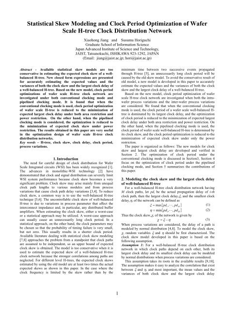
Statistical Skew Modeling and Clock Period Optimization of Wafer ...
Statistical Skew Modeling and Clock Period Optimization of Wafer ...
Statistical Skew Modeling and Clock Period Optimization of Wafer ...

Create successful ePaper yourself
Turn your PDF publications into a flip-book with our unique Google optimized e-Paper software.
<strong>Statistical</strong> <strong>Skew</strong> <strong>Modeling</strong> <strong>and</strong> <strong>Clock</strong> <strong>Period</strong> <strong>Optimization</strong> <strong>of</strong> <strong>Wafer</strong><br />
Scale H-tree <strong>Clock</strong> Distribution Network<br />
Xiaohong Jiang <strong>and</strong> Susumu Horiguchi<br />
Graduate School <strong>of</strong> Information Science<br />
Japan Advanced Institute <strong>of</strong> Science <strong>and</strong> Technology,<br />
JAIST, Tatsunokuchi, ISHIKAWA 923-1292, JAPAN<br />
(Email: jiang@jaist.ac.jp; hori@jaist.ac.jp)<br />
Abstract - Available statistical skew models are too<br />
conservative in estimating the expected clock skew <strong>of</strong> a wellbalanced<br />
H-tree. New closed form expressions are presented<br />
for accurately estimating the expected values <strong>and</strong> the<br />
variances <strong>of</strong> both the clock skew <strong>and</strong> the largest clock delay <strong>of</strong><br />
a well-balanced H-tree. Based on the new model, clock period<br />
optimizations <strong>of</strong> wafer scale H-tree clock network are<br />
investigated under both conventional clocking mode <strong>and</strong><br />
pipelined clocking mode. It is found that when the<br />
conventional clocking mode is used, clock period optimization<br />
<strong>of</strong> wafer scale H-tree is reduced to the minimization <strong>of</strong><br />
expected largest clock delay under both area restriction <strong>and</strong><br />
power restriction. On the other h<strong>and</strong>, when the pipelined<br />
clocking mode is considered, the optimization is reduced to<br />
the minimization <strong>of</strong> expected clock skew under power<br />
restriction. The results obtained in this paper are very useful<br />
in the optimization design <strong>of</strong> wafer scale H-tree clock<br />
distribution networks.<br />
Key words – H-tree, clock skew, clock delay, clock period,<br />
process variations.<br />
1. Introduction<br />
The need for careful design <strong>of</strong> clock distribution for <strong>Wafer</strong><br />
Scale Integrated circuits (WSI) has been widely recognized [1].<br />
The advances in monolithic-WSI technology [2] have<br />
demonstrated that clock <strong>and</strong> signal distribution can severely limit<br />
WSI system performance because clock skew becomes a very<br />
significant problem. <strong>Clock</strong> skew may arise mainly from unequal<br />
clock path lengths to various modules <strong>and</strong> from process<br />
variations that cause clock path delay variations [3,4]. To reduce<br />
clock skew, a common way is to use the well-balanced H-tree<br />
technique [5,6]. The uncontrollable clock skew <strong>of</strong> well-balanced<br />
H-tree is due to variations in process parameter that affect the<br />
interconnect impedance <strong>and</strong>, in particular, any distributed buffer<br />
amplifiers. When estimating the clock skew, either a worst-case<br />
or a statistical approach may be utilized. A worst-case approach<br />
can usually cause an unnecessarily long clock period. In a<br />
statistical approach, on the other h<strong>and</strong>, the clock parameters may<br />
be chosen so that the probability <strong>of</strong> timing failure is very small,<br />
but not zero. This usually results in a shorter clock period.<br />
Available literature dealing with statistical clock skew modeling<br />
[7,8] approaches the problem from a st<strong>and</strong>point that clock paths<br />
are assumed to be independent, so an upper bound <strong>of</strong> expected<br />
clock skew is obtained. The model is too conservative when it is<br />
used to estimate the expected skew <strong>of</strong> a well-balanced H-tree<br />
clock network because the stronger correlations among paths are<br />
neglected. For different level H-trees, the expected clock skews<br />
estimated by using the old model are at least two times the actual<br />
expected skews as shown in this paper. In the case where the<br />
clock frequency is limited by the skew rather than by the<br />
minimum time between two successive events propagated<br />
through H-tree [5], an unnecessarily long clock period will be<br />
caused by the old skew model. To avoid the conservative result <strong>of</strong><br />
old model, a new model is developed in this paper to accurately<br />
estimate the expected values <strong>and</strong> the variances <strong>of</strong> both the clock<br />
skew <strong>and</strong> the largest clock delay <strong>of</strong> a well-balanced H-tree.<br />
Based on the new model, clock period optimization <strong>of</strong> wafer<br />
scale H-tree clock network are investigated when both the intrawafer<br />
process variations <strong>and</strong> the inter-wafer process variations<br />
are considered. We found that when the conventional clocking<br />
mode is used, the clock period <strong>of</strong> a wafer scale well-balanced H-<br />
tree is dominated by its largest clock delay, <strong>and</strong> the optimization<br />
<strong>of</strong> clock period is reduced to the minimization <strong>of</strong> expected largest<br />
clock delay under both area restriction <strong>and</strong> power restriction. On<br />
the other h<strong>and</strong>, when the pipelined clocking mode is used, the<br />
clock period <strong>of</strong> wafer scale well-balanced H-tree is determined by<br />
its clock skew, <strong>and</strong> the clock period optimization is reduced to the<br />
minimization <strong>of</strong> expected clock skew under only the power<br />
restriction.<br />
The paper is organized as follows: The new models for clock<br />
skew <strong>and</strong> largest clock delay are developed <strong>and</strong> verified in<br />
Section 2. The optimization <strong>of</strong> clock period under the<br />
conventional clocking mode is discussed in Section3, Section 4<br />
focus on the optimization <strong>of</strong> clock period under the pipelined<br />
clocking mode, <strong>and</strong> Section 5 summarizes the contributions <strong>of</strong><br />
this paper.<br />
2. <strong>Modeling</strong> the clock skew <strong>and</strong> the largest clock delay<br />
<strong>of</strong> well-balanced H-tree<br />
For a well-balanced H-tree clock distribution network having<br />
M clock paths, let pd i be the actual propagation delay <strong>of</strong> i-th<br />
clock path, then the largest clock delay,, <strong>and</strong> the smallest clock<br />
delay,, <strong>of</strong> the network can be defined as<br />
max pd , 1<br />
, pd M<br />
<br />
(1)<br />
min pd , 1<br />
, pd M<br />
<br />
(2)<br />
Thus the clock skew,, <strong>of</strong> the network is given by<br />
<br />
(3)<br />
When process variations are considered, the delay <strong>of</strong> a path is<br />
modeled by normal distribution [4,8]. To model the clock skew,<br />
, r<strong>and</strong>om variables <strong>and</strong> should be first characterized. The<br />
clock skew model developed in this paper is based on the<br />
following assumption.<br />
Assumption 1: For a well-balanced H-tree clock distribution<br />
network in which clock paths depend on each other, both its<br />
largest clock delay <strong>and</strong> its smallest clock delay can be modeled<br />
by normal distributions when process variations are considered.<br />
This assumption takes its roots in the available results [9,10].<br />
The assumption makes it easy to analyze the correlation that exist<br />
between <strong>and</strong> , <strong>and</strong> most important, the mean values <strong>and</strong> the<br />
variances <strong>of</strong> both clock skew <strong>and</strong> the largest clock delay<br />
1
estimated by using the assumption are very accurate as shown in<br />
this paper.<br />
Before developing the model <strong>of</strong> clock skew <strong>and</strong> the largest<br />
clock delay, the H-tree itself must first be defined. Without loss<br />
<strong>of</strong> generality, the well-balanced H-tree has N hierarchical levels,<br />
where N denotes the tree depth. Level 0 branch corresponds to<br />
the root branch, <strong>and</strong> level N branches to the branches that support<br />
leaves. Level i branch begin with level i split point <strong>and</strong> end with<br />
level i+1 split point, with level 0 split point corresponds to<br />
primary clock input point. The H-tree illustrated in Fig.1 is drawn<br />
for N=8 (256 paths), which is used to distribute the clock signals<br />
to 256 processors implemented by WSI in a 4 -inch wafer.<br />
4.0 inch<br />
2.1 Evaluation <strong>of</strong> the mean values <strong>and</strong> the variances <strong>of</strong><br />
clock skew <strong>and</strong> the largest clock delay<br />
For a N hierarchical levels well-balanced H-tree, let d i , (i =<br />
0,…,N ) be actual delay <strong>of</strong> the i-th branch <strong>of</strong> a clock path, i be<br />
the largest clock delay <strong>and</strong> i be the smallest clock delay <strong>of</strong> the<br />
sub H-tree starting from i-th level split point. Then:<br />
max d , d <br />
i<br />
( i1)1<br />
( i1)1<br />
<br />
( i1)2<br />
( i1)2<br />
<br />
d<br />
( i1)1<br />
<br />
( i1)1<br />
<br />
d<br />
( i1)2<br />
<br />
( i1)2<br />
<br />
d<br />
( i1)1<br />
<br />
( i1)1<br />
<br />
d<br />
( i1)2<br />
<br />
( i1)2<br />
2<br />
<br />
i<br />
min d(<br />
i 1)1<br />
(<br />
i 1)1,<br />
d<br />
( i 1)2<br />
(<br />
i 1)2<br />
<br />
<br />
d<br />
<br />
d<br />
<br />
d<br />
<br />
d<br />
2<br />
( i 1)1<br />
( i 1)1<br />
( i 1)2<br />
( i 1)2<br />
Processors<br />
Buffer<br />
<strong>Clock</strong> Input<br />
Fig.1 An H-tree clock distribution network for 256 processors<br />
in a 4 inch WSI ( <strong>Clock</strong> buffers are not illustrated here).<br />
( i 1)1<br />
( i 1)1<br />
( i 1)2<br />
( i 1)2<br />
Where d (i+1)1 <strong>and</strong> d (i+1)2 are independent samples <strong>of</strong> d (i+1) , (i+1)1<br />
<strong>and</strong> (i+1)2 are independent samples <strong>of</strong> (i+1) , (i+1)1 <strong>and</strong> (i+1)2 are<br />
independent samples <strong>of</strong> (i+1) . Based on the Assumption 1, the<br />
mean values <strong>and</strong> the variances <strong>of</strong> i <strong>and</strong> i are given by following<br />
expressions based on the symmetry <strong>of</strong> well-balanced H-tree <strong>and</strong><br />
the properties <strong>of</strong> normal variables [11].<br />
D(<br />
di<br />
1)<br />
D(<br />
i<br />
1)<br />
(4)<br />
E(<br />
<br />
i<br />
) E(<br />
di<br />
1)<br />
E(<br />
i<br />
1)<br />
<br />
<br />
D(<br />
d<br />
i1)<br />
D(<br />
i<br />
1)<br />
(5)<br />
E(<br />
i<br />
) E(<br />
d<br />
i1)<br />
E(<br />
i<br />
1)<br />
<br />
<br />
1<br />
1<br />
D( i<br />
) D(<br />
di<br />
1)<br />
D(<br />
i<br />
1)<br />
D( i<br />
) D(<br />
di<br />
1)<br />
D(<br />
i<br />
1)<br />
<br />
(6)<br />
<br />
<br />
<br />
Where E() <strong>and</strong> D() represent the mean value <strong>and</strong> the variance <strong>of</strong><br />
a r<strong>and</strong>om variable, respectively.<br />
Above process indicate clearly that E( i ), D( i ), E( i ) <strong>and</strong><br />
D( i ) can be obtained by using E( i+1 ), D( i+1 ), E( i+1 ), D( i+1 ),<br />
E(d i+1 ) <strong>and</strong> D(d i+1 ).Then a recursive approach is obtained to<br />
evaluate the mean values <strong>and</strong> the variances <strong>of</strong> both the largest<br />
clock delay <strong>and</strong> the smallest clock delay <strong>of</strong> a well-balanced H-<br />
tree.<br />
Applying (4)-(6) to the N level well-balanced H-tree<br />
recursively, we have:<br />
E<br />
E<br />
N<br />
1<br />
k 1<br />
<br />
<br />
Ed<br />
i<br />
<br />
<br />
Dd<br />
N ik<br />
<br />
i0<br />
N<br />
1<br />
<br />
1<br />
N<br />
i1 k 1<br />
1<br />
k 1<br />
<br />
<br />
Ed<br />
i<br />
<br />
<br />
Dd<br />
N ik<br />
<br />
i0<br />
<br />
N<br />
i1 k 1<br />
N<br />
1<br />
D D Dd<br />
i<br />
<br />
(9)<br />
( )<br />
<br />
i0<br />
<br />
The results <strong>of</strong> (7)-(9) <strong>and</strong> (3) indicate that the expected clock<br />
skew <strong>and</strong> the variance <strong>of</strong> the skew <strong>of</strong> a N level well-balanced H-<br />
tree can be estimated by:<br />
N i<br />
2<br />
k 1<br />
(10)<br />
1<br />
E<br />
<br />
E<br />
<br />
E<br />
<br />
Dd<br />
N i<br />
k<br />
<br />
<br />
i 1 k 1<br />
N<br />
i<br />
1<br />
(11)<br />
D<br />
<br />
D<br />
<br />
D<br />
<br />
2 r D<br />
<br />
D<br />
2 (1 r)<br />
Dd<br />
i<br />
<br />
i 0 <br />
Where r is the correlation coefficient <strong>of</strong> <strong>and</strong> , <strong>and</strong> r can be<br />
recursively evaluated for a network [20]. It can be seen from (10)<br />
that the mean value <strong>of</strong> clock skew <strong>of</strong> a well-balanced H-tree is<br />
determined completely by the variances <strong>of</strong> branches delay, <strong>and</strong><br />
the clock skew is accumulated in a complicated way.<br />
2.2 <strong>Statistical</strong> model for <strong>Wafer</strong> scale H-tree<br />
The parameters variations in the manufacturing process <strong>of</strong><br />
CMOS digital circuits cause path delays to deviate from the<br />
designed values, <strong>and</strong> thus cause clock skew in a well-balanced H-<br />
tree. These variations are usually classified as intra-die variation,<br />
inter-die variation, intra-wafer variation, inter-wafer variation,<br />
intra-lot variation, <strong>and</strong> inter-lot variation, etc. Since we are<br />
interested in the wafer-scale H-tree, so only the intra-wafer <strong>and</strong><br />
the inter-wafer variations are considered in the statistical<br />
modeling to avoid arriving at intractably complex models.<br />
In general, inter-wafer <strong>and</strong> intra-wafer parameters variations<br />
can be modeled by normal distributions or uniform distributions<br />
[12]. Here the normal distributions are used, but the results<br />
i<br />
obtained can easily be extended to other distributions. Let p<br />
inter<br />
be the value <strong>of</strong> i-th parameter determined only by the inter-wafer<br />
i i<br />
normal variations N ( <br />
inter<br />
, <br />
inter<br />
) with mean value, <br />
i , <strong>and</strong><br />
inter<br />
i<br />
inter-wafer st<strong>and</strong>ard deviation, , then the actual value <strong>of</strong> the<br />
inter<br />
parameter will be determined by the normal distribution<br />
i i<br />
i<br />
N ( p inter<br />
, <br />
intra<br />
) with mean value, p , <strong>and</strong> intra-wafer<br />
inter<br />
st<strong>and</strong>ard deviation, <br />
i . Thus, when both the inter-wafer <strong>and</strong><br />
intra<br />
intra-wafer variations are considered, the actual value p i <strong>of</strong> i-th<br />
process parameter can be expressed as<br />
i i<br />
i i<br />
p pinter<br />
<br />
intra<br />
<br />
intra<br />
(12)<br />
i<br />
i<br />
i i<br />
<br />
<br />
inter<br />
inter<br />
i<br />
intra<br />
inter<br />
<br />
inter<br />
, N (0,1)<br />
Where is the r<strong>and</strong>om variables associated with inter-wafer<br />
inter<br />
parameter variations <strong>and</strong> will be same for all process parameters<br />
in a wafer. i is the r<strong>and</strong>om variable associated with the<br />
intra<br />
intra-wafer variation <strong>of</strong> i-th parameter. <br />
i is independent <strong>of</strong><br />
intra<br />
i<br />
, <strong>and</strong> the correlation between<br />
inter<br />
reflects the correlation<br />
intra<br />
between parameters.<br />
For a fixed value <strong>of</strong> r<strong>and</strong>om variable (i.e. when only the<br />
inter<br />
intra-wafer variations are considered), the mean values <strong>and</strong> the<br />
variances <strong>of</strong> clock skew <strong>and</strong> the largest clock delay <strong>of</strong> wafer scale<br />
H-tree are only determined by intra-wafer parameter variations<br />
i<br />
i<br />
intra<br />
i<br />
intra<br />
(7)<br />
(8)<br />
2
<strong>and</strong> given by (7)-(11), <strong>and</strong> these values will vary with the<br />
variation <strong>of</strong> inter<br />
. Thus, when both the inter-wafer <strong>and</strong> intrawafer<br />
are considered, the mean values <strong>and</strong> the variances <strong>of</strong> clock<br />
skew <strong>and</strong> the largest clock delay <strong>of</strong> wafer scale H-tree can be<br />
modeled as:<br />
2<br />
N<br />
N i<br />
inter<br />
<br />
1 <br />
1 k 1<br />
1 (13)<br />
<br />
2<br />
E<br />
Edi<br />
<br />
<br />
Dd<br />
N i k<br />
<br />
<br />
<br />
e d<br />
inter<br />
<br />
<br />
i0<br />
<br />
<br />
i1 k1<br />
2<br />
2<br />
N i<br />
inter<br />
<br />
2 <br />
k 1<br />
1 (14)<br />
1<br />
<br />
2<br />
E<br />
<br />
<br />
Dd<br />
N i k<br />
<br />
<br />
<br />
e d<br />
inter<br />
<br />
<br />
<br />
i1 k 1<br />
2<br />
N<br />
i<br />
2<br />
inter<br />
<br />
<br />
D<br />
<br />
1 <br />
<br />
1<br />
(15)<br />
2<br />
D(<br />
di<br />
) <br />
<br />
e<br />
<br />
d<br />
inter<br />
<br />
<br />
i1<br />
<br />
2<br />
2<br />
N<br />
i<br />
inter<br />
<br />
1 1 <br />
D<br />
<br />
<br />
(16)<br />
2<br />
2 (1 r)<br />
D(<br />
di<br />
) <br />
<br />
e d<br />
inter<br />
<br />
<br />
i 1<br />
<br />
<br />
2<br />
2.3 Yield estimates for skew <strong>and</strong> the largest delay<br />
The clock period <strong>of</strong> a H-tree network is in general determined<br />
by both the clock skew <strong>and</strong> the largest clock delay <strong>of</strong> the<br />
network. With the estimates <strong>of</strong> mean values <strong>and</strong> the st<strong>and</strong>ard<br />
deviations <strong>of</strong> both <strong>and</strong> in h<strong>and</strong>, it is possible for us to estimate<br />
the yields <strong>of</strong> <strong>and</strong> . As indicated in the Assumption 1, the yield<br />
<strong>of</strong> can be estimated by normal distribution N(E(),D()) with<br />
mean, E(), <strong>and</strong> variance, D(). On the other h<strong>and</strong>, clock skew<br />
can be modeled by log-normal distribution as verified by<br />
extensive simulation results [10]. Then the clock skew yield, i.e.<br />
the probability that the actual skew <strong>of</strong> the network, , is less than<br />
a skew specification x (P( x)), can be evaluated as:<br />
2<br />
x loge<br />
1 logt<br />
(17)<br />
P(<br />
x)<br />
exp<br />
dt<br />
0<br />
2<br />
<br />
t<br />
<br />
2 <br />
Here parameters <strong>and</strong> are given by:<br />
<br />
2<br />
(18)<br />
E ( )<br />
log<br />
<br />
2<br />
D ( ) E<br />
( ) <br />
2<br />
D ( ) E<br />
( ) <br />
<br />
(19)<br />
log e log <br />
2<br />
E ( ) <br />
So once the mean values <strong>and</strong> the variances <strong>of</strong> both <strong>and</strong> are<br />
estimated by the model developed in Section 2.2, the yields <strong>of</strong> <br />
<strong>and</strong> can be estimated by the normal <strong>and</strong> log-normal<br />
distributions, respectively.<br />
2.4 Old skew model for H-tree<br />
Under the assumption that all the paths are independent, an<br />
upper bound <strong>of</strong> expected clock skew E upper () <strong>of</strong> a well-balanced<br />
H-tree is asymptotically given by [7]:<br />
4ln<br />
M ln ln M ln 4<br />
2C<br />
1 <br />
(20)<br />
E upper <br />
<br />
1<br />
<br />
1<br />
O<br />
<br />
2<br />
2ln<br />
M <br />
log M <br />
With the variance <strong>of</strong> clock skew is given by<br />
2 2<br />
1<br />
1 <br />
(21)<br />
<br />
<br />
O<br />
D upper 2<br />
6ln M log M<br />
Where 1 is the st<strong>and</strong>ard deviation <strong>of</strong> path delay, C=0.5772… is<br />
Euler’s constant, <strong>and</strong> O() is the higher order terms. When both<br />
the inter-wafer <strong>and</strong> intra-wafer are considered, the expected skew<br />
E upper () <strong>and</strong> the variance D upper () <strong>of</strong> the old model should also<br />
be evaluated as that <strong>of</strong> (13)-(16) .<br />
2.5 Verification <strong>of</strong> the new model<br />
To verify the new skew model, extensive simulations <strong>and</strong><br />
theoretical calculations are conducted that based on an assumed<br />
<br />
<br />
10.010.0 cm 2 WSI as illustrated in Fig.1, along with an 1616<br />
array <strong>of</strong> medium grained processing elements (PE) each with<br />
4.04.0 mm 2 effective area <strong>and</strong> 6.06.0 mm 2 tile area in 1m<br />
CMOS technology * . The process parameters <strong>and</strong> estimation <strong>of</strong><br />
delay variation are based on a predicted 1m CMOS technology<br />
[8]. As that did in [13], the inter-wafer st<strong>and</strong>ard deviation <strong>of</strong> a<br />
process parameter is assumed to be 15% <strong>of</strong> its inter-wafer<br />
nominal, <strong>and</strong> the intra-wafer st<strong>and</strong>ard deviation <strong>of</strong> a process<br />
parameter is assumed to be 10% <strong>of</strong> its intra-wafer nominal. Based<br />
on the mean delay value <strong>and</strong> the delay variance <strong>of</strong> each branch,<br />
both simulation <strong>and</strong> the theoretical approach can be used to<br />
estimate the clock skew <strong>and</strong> the largest clock delay <strong>of</strong> a H-tree. In<br />
theoretical approach, algorithm presented in Section 2.2 is used to<br />
evaluate the parameters E(), E(), D() <strong>and</strong> D() <strong>of</strong> the H-tree.<br />
In the simulation approach, the actual delay <strong>of</strong> a branch is<br />
simulated by a normal r<strong>and</strong>om variable. The actual delay <strong>of</strong> a<br />
path is the sum <strong>of</strong> these actual delays <strong>of</strong> the branches along the<br />
path. Then actual largest clock delay, the smallest clock delay<br />
<strong>and</strong> the clock skew <strong>of</strong> the H-tree can be simulated by the<br />
expressions (1)-(3). Parts <strong>of</strong> the simulation results <strong>and</strong> theoretical<br />
results are summarized in Fig.2 – Fig.4.<br />
mean value <strong>of</strong> clock skew, ps<br />
2500<br />
2000<br />
1500<br />
1000<br />
500<br />
theoretical results <strong>of</strong> new model<br />
simulation results<br />
theoretical results <strong>of</strong> old model<br />
results <strong>of</strong> passive H-tree<br />
results <strong>of</strong> buffered H-tree<br />
0<br />
2 3 4 5 6 7 8<br />
hieratical levels <strong>of</strong> H-tree ,N ( path number is 2 N )<br />
Fig.2 Simulation results <strong>and</strong> theoretical results in mean<br />
values <strong>of</strong> clock skew.<br />
mean value <strong>of</strong> largest clock delay, ns<br />
40<br />
30<br />
20<br />
10<br />
0<br />
theoretical results <strong>of</strong> new model<br />
simulation results<br />
results <strong>of</strong> passive H-tree<br />
results <strong>of</strong> buffered H-tree<br />
2 3 4 5 6 7 8<br />
hieratical levels <strong>of</strong> H-tree ,N ( path number is 2 N )<br />
Fig.3 Simulation results <strong>and</strong> theoretical results in mean<br />
values <strong>of</strong> the largest clock delay.<br />
* A processing element with significant local memory <strong>and</strong> processing<br />
power would <strong>of</strong> course be much larger. However, we are considering<br />
medium grain PE’s so that 4mm4mm is a reasonable size for this case<br />
example.<br />
3
st<strong>and</strong>ard deviation <strong>of</strong> clock skew <strong>and</strong><br />
largest clock delay, ps<br />
450<br />
400<br />
350<br />
300<br />
250<br />
200<br />
150<br />
100<br />
50<br />
0<br />
st<strong>and</strong>ard deviation <strong>of</strong> clock skew estimated by new model<br />
simulation results <strong>of</strong> st<strong>and</strong>ard deviation <strong>of</strong> clock skew<br />
st<strong>and</strong>ard deviation <strong>of</strong> clock skew estimated by old model<br />
st<strong>and</strong>ard deviation <strong>of</strong> largest clock delay estimated by new model<br />
simulation results <strong>of</strong> st<strong>and</strong>ard deviation <strong>of</strong> largest clock delay<br />
results <strong>of</strong> buffered H-tree<br />
results <strong>of</strong> passive H-tree<br />
2 3 4 5 6 7 8<br />
hieratical levels <strong>of</strong> H-tree, N (path number is 2 N )<br />
Fig.4 Simulation results <strong>and</strong> theoretical results in variances <strong>of</strong><br />
clock skew <strong>and</strong> the largest clock delay.<br />
To verify furthermore the yield models presented in Section<br />
2.3, the simulation results <strong>and</strong> the theoretical results in yields <strong>of</strong><br />
skew <strong>and</strong> the largest delay <strong>of</strong> the wafer scale H-tree are<br />
summarized in Fig.5 <strong>and</strong> Fig.6. Here m inverters are inserted in<br />
each clock path, each inverter is h times the minimum inverter <strong>of</strong><br />
1m CMOS technology, <strong>and</strong> line width <strong>of</strong> the clock path is W.<br />
Two combinations <strong>of</strong> m, h <strong>and</strong> W are used in the verification. For<br />
comparison, we also provide in Fig.5 the simulation results <strong>of</strong><br />
yield <strong>of</strong> clock skew when all paths are assumed independent.<br />
probability that clock skew is less than x<br />
1.0<br />
0.8<br />
0.6<br />
0.4<br />
0.2<br />
0.0<br />
Simulation results <strong>of</strong> skew Theoretical results <strong>of</strong> skew<br />
Simulation results <strong>of</strong> skew when all paths are assumed independent<br />
(1) h=15, w=5 m, m=136 (2) h=30, w=10 m, m=272<br />
(2)<br />
(1)<br />
(2)<br />
600 800 1000 1200 1400 1600 1800 2000 2200 2400<br />
(1)<br />
required clock skew x, ps<br />
Fig.5 Simulation results <strong>and</strong> the theoretical results in yield<br />
<strong>of</strong> clock skew <strong>of</strong> H-tree for two combinations <strong>of</strong> parameters<br />
m, h <strong>and</strong> W.<br />
probability that the largest clock delay<br />
is less than x<br />
1.0<br />
0.8<br />
0.6<br />
0.4<br />
0.2<br />
Simulation results <strong>of</strong> the largest clock delay<br />
Theoretical results <strong>of</strong> the largest clock delay<br />
(1) h=15, w=5 m, m=136 (2) h=30, w=10 m, m=272<br />
(1)<br />
0.0<br />
21500 22000 22500 23000 23500 24000 24500<br />
required value <strong>of</strong> the largest clock delay x, ps<br />
Fig.6 Simulation results <strong>and</strong> the theoretical results in yield <strong>of</strong><br />
the largest clock delay <strong>of</strong> H-tree for two combinations <strong>of</strong><br />
parameters m, h <strong>and</strong> W.<br />
(2)<br />
The results in Fig.2 show clearly that the old model is too<br />
conservative when it is used to estimate the expected skew <strong>of</strong> a<br />
well-balanced H-tree, the expected skew estimated by old model<br />
is at least two times the actual expected skew for different level<br />
H-tree. The yield results in Fig.5 illustrate further that the<br />
assumption <strong>of</strong> old model that all clock paths are independent is<br />
too conservative in estimating the clock skew <strong>of</strong> H-tree. In the<br />
case where the clock frequency is limited by the skew rather than<br />
by the minimum time between two successive events propagated<br />
through the H-tree [5], an unnecessarily long clock period will be<br />
caused by using the old skew model.<br />
On the other h<strong>and</strong>, the new model developed in this paper can<br />
be used to get an accurate estimate <strong>of</strong> mean values <strong>and</strong> variances<br />
for both the clock skew <strong>and</strong> the largest clock delay <strong>of</strong> a wellbalanced<br />
H-tree as shown in Fig.2-Fig.4, so the too conservative<br />
results <strong>of</strong> old skew model can be avoided by using the new<br />
model. The yield results in Fig.5 <strong>and</strong> Fig.6 indicate that when the<br />
mean values <strong>and</strong> variances <strong>of</strong> both the clock skew <strong>and</strong> the largest<br />
clock delay are accurately estimated, the yields <strong>of</strong> clock skew <strong>and</strong><br />
the largest clock delay <strong>of</strong> H-tree can be further accurately<br />
estimated by log-normal <strong>and</strong> normal distribution, respectively.<br />
Furthermore, the closed expressions (13)-(16) indicate clearly<br />
how the clock skew <strong>and</strong> the largest clock delay are accumulated<br />
along the clock paths <strong>and</strong> with the increase <strong>of</strong> H-tree size. This<br />
enable a suitable H-tree size is selected for a specified clock<br />
frequency, <strong>and</strong> this also enable the optimization to be made to<br />
minimize the clock period <strong>and</strong> thus improve the speed for a fixed<br />
size H-tree network. In the following two Sections, we focus on<br />
the clock period optimization <strong>of</strong> the wafer scale H-tree in Fig.1.<br />
3. <strong>Clock</strong> period optimization <strong>of</strong> wafer scale H-tree in<br />
the conventional clocking mode<br />
By using the conventional clocking method, the clock period, T,<br />
is required to be greater than the longest clock delay,. Another<br />
requirement is the 10% rule <strong>of</strong> thumb relating the skew,, to the<br />
clock period [5]. Thus the clock period must be<br />
T max , 10 <br />
(22)<br />
Due to the very symmetrical design <strong>of</strong> well-balanced H-tree, a<br />
lower clock skew is expected, but larger propagation delay from<br />
clock input to a processor will be caused because <strong>of</strong> its relative<br />
long clock path. We can reduce the propagation delay by<br />
appropriately inserting drivers (inverters) in a clock path. For a<br />
H-tree path, drivers can be inserted as shown in Fig.7<br />
Root<br />
: Line Segment : Driver<br />
If k inverters which is h times the minimum inverter are inserted<br />
in the path, the propagation delay, d Propagation , <strong>of</strong> the path is given<br />
by [14]:<br />
d k T<br />
Propagatio n<br />
segment<br />
Processor<br />
Fig. 7 Insertion <strong>of</strong> drivers in an H-tree metallic path.<br />
R0<br />
Cint<br />
Rint<br />
Cint<br />
(23)<br />
T segment<br />
2.3<br />
hC<br />
0 2.3hC<br />
0 <br />
h k k k <br />
Where T segment is the delay per line segment, C 0 <strong>and</strong> R 0 are the<br />
input capacitance <strong>and</strong> output resistance <strong>of</strong> the minimum size<br />
inverter, C int <strong>and</strong> R int are the capacitance <strong>and</strong> resistance <strong>of</strong> the<br />
interconnection line in the path. These parameters are given by:<br />
4
R<br />
L<br />
W<br />
T T<br />
0<br />
, C<br />
Cox<br />
( VDD<br />
V<br />
0<br />
T<br />
)<br />
C<br />
ox<br />
W<br />
L<br />
Rint<br />
Lint<br />
Wint<br />
t , Cint<br />
Wint<br />
Lint<br />
t ox<br />
(24)<br />
Where W T <strong>and</strong> L T are the width <strong>and</strong> length <strong>of</strong> the transistor, C ox<br />
is the gate unit area capacitance, is the charge carrier mobility,<br />
V T is the threshold voltage, is the metal resistivity, <strong>and</strong> is the<br />
oxide dielectric constant. Here the interconnection line is with<br />
width W int , length L int <strong>and</strong> thickness t on an oxide layer <strong>of</strong><br />
thickness t ox . By setting derivatives <strong>of</strong> d Propagation with respect to k<br />
<strong>and</strong> h to zero, optimal values for k <strong>and</strong> h can be obtained to<br />
minimize the propagation delay <strong>of</strong> the path [14].<br />
Note from (13) <strong>and</strong> (14) that the mean value <strong>of</strong> the largest<br />
clock delay <strong>of</strong> a well-balanced H-tree is determined by both the<br />
expected delay <strong>of</strong> single path <strong>and</strong> the expected skew <strong>of</strong> the H-tree.<br />
Here the expected delay <strong>of</strong> a path is determined by the expected<br />
branches delay in the path. On the other h<strong>and</strong>, the expected clock<br />
skew is determined by the variances <strong>of</strong> the branches delay in the<br />
path. The minimum <strong>of</strong> mean value <strong>and</strong> variance <strong>of</strong> path delay<br />
usually do not occur for the same combination <strong>of</strong> driver number<br />
<strong>and</strong> driver size [8]. Thus minimizing path delay does neither<br />
guarantee minimum skew nor minimum largest clock delay, it is<br />
just a heuristic design that turn out to provide a good trade<strong>of</strong>f<br />
between clock skew <strong>and</strong> the largest clock delay.<br />
The results in Section 2 <strong>and</strong> above analysis indicate that the<br />
clock skew <strong>and</strong> the largest clock delay <strong>of</strong> a well-balanced H-tree<br />
are completely determined by the mean values <strong>and</strong> the variances<br />
<strong>of</strong> branches delay. The mean value <strong>and</strong> the variance <strong>of</strong> a branch<br />
delay are the sum <strong>of</strong> the mean delay values <strong>and</strong> the delay<br />
variances <strong>of</strong> the line segments in the branch (here we insert at<br />
least one driver in each branch to make the analysis easy),<br />
respectively. The mean value <strong>of</strong> a line segment can be obtained<br />
by using (23), <strong>and</strong> one approach to calculate the delay variance <strong>of</strong><br />
a line segment due to the variations <strong>of</strong> process parameters is to<br />
express the relation (23) in terms <strong>of</strong> independent variables. These<br />
variables are geometrical dimensions, C ox (unit area gate oxide<br />
capacitance), (carrier mobility), <strong>and</strong> V T (threshold voltage). All<br />
these factors can be considered independent [8,15]. Thus, the<br />
variance <strong>of</strong> a line segment can be determined in terms <strong>of</strong><br />
variances <strong>of</strong> these independent r<strong>and</strong>om variables. For example,<br />
the variance, <br />
2 , <strong>of</strong> a r<strong>and</strong>om variable Z that is a function <strong>of</strong><br />
Z<br />
some independent r<strong>and</strong>om variables, z f ( x,<br />
y,<br />
)<br />
may be<br />
obtained from<br />
2<br />
2 f<br />
2 f<br />
2<br />
(25)<br />
<br />
z<br />
<br />
x<br />
<br />
y<br />
<br />
x<br />
y<br />
<br />
To find the effects <strong>of</strong> drivers on the clock skew <strong>and</strong> on the<br />
largest clock delay, the new model developed in Section 2 is used<br />
to evaluate the wafer scale H-tree clock network shown in Fig.1.<br />
Here, process parameters are based on the predicted 1m CMOS<br />
technology [8,16]. The PE area, tile area <strong>and</strong> the variations <strong>of</strong><br />
process parameters are same as that <strong>of</strong> Section 2.5, the width <strong>of</strong><br />
interconnection line is set as W int =10m. Fig.8 illustrates the<br />
trends <strong>of</strong> the mean values E() <strong>and</strong> E(10) <strong>of</strong> the H-tree with the<br />
variations <strong>of</strong> driver number <strong>and</strong> driver size in each path.<br />
The results in Fig.8 indicate clearly that in the conventional<br />
clocking mode, the actual clock period <strong>of</strong> well-balanced H-tree<br />
clock distribution is dominated by its largest clock delay rather<br />
than by its clock skew. For a driver size, there exist an optimal<br />
number <strong>of</strong> drivers (about 100 in each path) to minimize the mean<br />
value <strong>of</strong> the largest clock delay <strong>and</strong> thus the clock period <strong>of</strong> the<br />
H-tree. Therefore, in the conventional clocking mode,<br />
2<br />
T<br />
T<br />
minimization <strong>of</strong> clock period <strong>of</strong> well-balanced H-tree can be<br />
implemented by minimizing its largest clock delay. To assure that<br />
H-tree can works with high probability around the optimized<br />
clock period, the variances <strong>of</strong> the largest clock delay should also<br />
be considered. By finding the minimum clock period for different<br />
driver size, <strong>and</strong> calculating the corresponding variance, we can<br />
construct a plot <strong>of</strong> st<strong>and</strong>ard deviation vs. mean value <strong>of</strong> the<br />
largest clock delay (clock period) as shown in Fig.9.<br />
mean values <strong>of</strong> largest clock delay<br />
<strong>and</strong> 10 times clock skew, ns<br />
50<br />
40<br />
30<br />
20<br />
10<br />
0<br />
st<strong>and</strong>ard deviation <strong>of</strong><br />
the largest clock delay, ps<br />
results <strong>of</strong> 40 times<br />
minimum size inverter<br />
0 100 200 300 400<br />
number <strong>of</strong> inverter<br />
800<br />
600<br />
400<br />
200<br />
mean value <strong>of</strong> largest clock delay<br />
mean value <strong>of</strong> 10 times clock skew<br />
results <strong>of</strong> 20 times<br />
minimum size inverter<br />
results <strong>of</strong> 30 times<br />
minimum size inverter<br />
Fig.8 The trends <strong>of</strong> expected values <strong>of</strong> clock skew <strong>and</strong> the<br />
largest clock delay with the variations <strong>of</strong> driver number <strong>and</strong><br />
driver size in each path.<br />
10 20 30 40 50 60<br />
mean value <strong>of</strong> the largest clock delay, ns<br />
Fig.9 St<strong>and</strong>ard deviation vs. mean value <strong>of</strong> the largest clock<br />
delay.<br />
Fig.9 illustrates a similar relationship as obtained in [17], the<br />
st<strong>and</strong>ard deviation <strong>of</strong> the largest clock delay decreases linearly<br />
with the decrease <strong>of</strong> its mean value. Thus, in the conventional<br />
clocking mode, the minimization <strong>of</strong> clock period <strong>of</strong> wafer scale<br />
H-tree can be simply reduced to the minimization <strong>of</strong> the mean<br />
value <strong>of</strong> the largest clock delay.<br />
It is well known that by increasing the driver size, the<br />
minimum clock period can be further reduced as illustrated in the<br />
Fig.8. However, beyond a certain point that the period<br />
improvement becomes costly in both area <strong>and</strong> power. By finding<br />
the minimum clock period for different driver size, <strong>and</strong><br />
calculating the corresponding average power dissipation <strong>and</strong> area<br />
<strong>of</strong> the network, we can construct a plot <strong>of</strong> power <strong>and</strong> area vs. the<br />
largest clock delay (clock period) as shown in Fig.10. The results<br />
in Fig.10 show that in the conventional clocking mode, reducing<br />
in clock period carries both extra area <strong>and</strong> extra power penalty.<br />
Furthermore, all <strong>of</strong> the additional area is in active silicon<br />
(transistor sizing) so that yield <strong>and</strong> reliability are reduced while<br />
power dissipation is increased, so both the area requirement <strong>and</strong><br />
power requirement should be considered in the optimization <strong>of</strong><br />
clock period.<br />
5
area <strong>and</strong> power dissipation<br />
32<br />
30<br />
28<br />
26<br />
24<br />
22<br />
20<br />
6<br />
4<br />
2<br />
0<br />
Area, mm 2<br />
Power dissipation , W<br />
10 20 30 40 50 60<br />
largest clock delay, ns<br />
Fig.10 Power <strong>and</strong> area vs. the expected largest clock delay<br />
(notice that the two curves do not follow the same ordinate<br />
scale: one is a area <strong>and</strong> the other is a power).<br />
Therefore, in the conventional clocking mode, the clock period<br />
optimization <strong>of</strong> wafer scale well-balanced H-tree can be<br />
formulated as:<br />
2<br />
Minimize N<br />
N i<br />
inter<br />
<br />
1<br />
1 k1<br />
1 <br />
<br />
<br />
2<br />
Ed<br />
i<br />
Dd<br />
N i k<br />
<br />
<br />
e d<br />
<br />
<br />
<br />
int er<br />
<br />
<br />
i0<br />
<br />
<br />
i1 k 1<br />
2<br />
Area A<br />
subject to<br />
spec<br />
(26)<br />
Power Pspec<br />
In practice, one can perform this optimization by using the<br />
genetic algorithms [21]. For example, when the area requirement<br />
is 25mm 2 <strong>and</strong> power dissipation requirement is 4 W, we found the<br />
minimum mean value <strong>of</strong> the largest clock delay, E <br />
, is 17.8 ns,<br />
<strong>and</strong> the corresponding st<strong>and</strong>ard deviation D <br />
given by (15)<br />
is 228 ps. This occurs when number <strong>of</strong> the drivers is 100 in each<br />
path <strong>and</strong> the size <strong>of</strong> the drivers is 40 times the minimum size<br />
inverter. To assure a very high (>99%) probability <strong>of</strong> system<br />
success, we chose a confidence level <strong>of</strong> 3 D<br />
based on the<br />
normal distribution as discussed in Section 2.3. Then the H-tree<br />
can works with very high (>99%) probability at frequency larger<br />
than 1 E ( ) 3 D(<br />
) 54MHz<br />
.<br />
4. <strong>Clock</strong> period optimization <strong>of</strong> wafer scale H-tree in<br />
the pipelined clocking mode<br />
The results in Section 3 show that in the conventional clocking<br />
mode, the clock period <strong>of</strong> a well-balanced H-tree network is<br />
seriously limited by its largest clock delay that is usually larger<br />
for H-tree clock network. The limitation can be released by using<br />
the pipeline techniques [5][18]. Given the fact that Fig.7 path<br />
structure <strong>of</strong> a well-balanced H-tree is pipelined, to insert the same<br />
kind <strong>of</strong> event (transition to zero or one), one just has to wait until<br />
the previous occurrence <strong>of</strong> the event propagates to the third stage.<br />
Again, another requirement is the 10% rule <strong>of</strong> thumb relating the<br />
skew to the clock period. Thus, the clock period will be<br />
T max2<br />
Tsegment<br />
, 10 <br />
(27)<br />
Fig.11 illustrates the trends <strong>of</strong> the mean values E(T segment ) <strong>and</strong> E()<br />
<strong>of</strong> the H-tree with the variations <strong>of</strong> driver number <strong>and</strong> driver size<br />
in each path.<br />
The results in Fig.11 indicate clearly that when drivers are used<br />
to divide clock paths into line segments, the mean delay <strong>of</strong> a line<br />
segment is considered smaller than the expected clock skew <strong>of</strong><br />
the H-tree. Thus, in the pipelined clocking mode, the clock period<br />
<strong>of</strong> wafer scale well-balanced H-tree is dominated by its clock<br />
skew rather than by the delay <strong>of</strong> a line segment. For a driver size,<br />
there exist an optimal number <strong>of</strong> drivers to minimize the mean<br />
value <strong>of</strong> the clock skew <strong>and</strong> thus the clock period <strong>of</strong> the H-tree.<br />
Therefore, in the pipelined clocking mode, minimization <strong>of</strong> clock<br />
period <strong>of</strong> well-balanced H-tree can be implemented by<br />
minimizing its clock skew.<br />
mean values <strong>of</strong> both skew <strong>and</strong><br />
the delay per line segment, ps<br />
For a driver size, it can be seen from Fig.8 <strong>and</strong> Fig.11 that the<br />
driver number required to minimize the clock period in the<br />
pipelined clocking mode is larger than that <strong>of</strong> conventional<br />
clocking mode. In the pipelined clocking mode, the clock period<br />
is dominated by clock skew, <strong>and</strong> the mean value <strong>of</strong> clock skew is<br />
governed by the variances <strong>of</strong> branches delay in a path. So the<br />
results in Fig.8 <strong>and</strong> Fig.11 indicate that the variation in<br />
capacitance due to the variations in line dimensions (width <strong>and</strong><br />
thickness) is the main cause in the path delay variation <strong>and</strong><br />
relative inverter delay variation is minor. The above discussion<br />
results in a same conclusion as that obtained in [8]. Drivers are<br />
effective in making the line delay linear with the line length, but<br />
they are even more effective in reducing the st<strong>and</strong>ard deviation <strong>of</strong><br />
the line delay.<br />
To assure that H-tree can works with high probability around<br />
the optimized clock period, the variances <strong>of</strong> the clock skew<br />
should also be considered. By finding the minimum clock period<br />
for different driver size, <strong>and</strong> calculating the corresponding<br />
variance, we can construct a plot <strong>of</strong> st<strong>and</strong>ard deviation vs. mean<br />
value <strong>of</strong> clock skew (clock period) as shown in Fig.12.<br />
st<strong>and</strong>ard deviation <strong>of</strong> clock skew, ps<br />
1600<br />
1400<br />
1200<br />
1000<br />
800<br />
600<br />
400<br />
200<br />
200<br />
150<br />
100<br />
mean value <strong>of</strong> clock skew<br />
mean value <strong>of</strong> the delay per line segment<br />
results <strong>of</strong> 20 times minimum size inverter<br />
results <strong>of</strong> 30 times minimum size inverter<br />
results <strong>of</strong> 40 times minimum size inverter<br />
0 400 800 1200 1600 2000<br />
number <strong>of</strong> inverter<br />
Fig.11 The trends <strong>of</strong> expected values <strong>of</strong> clock skew <strong>and</strong> line<br />
segment delay with the variations <strong>of</strong> driver number <strong>and</strong> driver<br />
size in each path.<br />
400 600 800 1000 1200<br />
mean value <strong>of</strong> clock skew, ps<br />
Fig.12 St<strong>and</strong>ard deviation vs. mean value <strong>of</strong> clock skew.<br />
6
Again, Fig.12 illustrates a similar linear relationship as that <strong>of</strong><br />
Fig.9. The st<strong>and</strong>ard deviation <strong>of</strong> clock skew also decreases<br />
linearly with the decrease <strong>of</strong> its mean value. Thus, in the<br />
pipelining clocking mode, the minimization <strong>of</strong> clock period can<br />
be simply reduced to the minimization <strong>of</strong> the mean value <strong>of</strong> clock<br />
skew.<br />
It is shown in Fig.11 that by increasing the driver size, the<br />
minimum clock period can be further reduced. By finding the<br />
minimum clock period for different driver size, <strong>and</strong> calculating<br />
the corresponding average power dissipation <strong>and</strong> area <strong>of</strong> the<br />
network, we can construct a plot <strong>of</strong> power <strong>and</strong> area vs. the clock<br />
skew (clock period) as shown in Fig.13.<br />
frequency <strong>of</strong> occurrence<br />
200<br />
150<br />
100<br />
50<br />
0<br />
2.5 2.6 2.7 2.8 2.9<br />
Common logarithm <strong>of</strong> clock skew, log()<br />
area <strong>and</strong> power dissipation<br />
45<br />
40<br />
35<br />
30<br />
25<br />
20<br />
15<br />
10<br />
5<br />
power dissipation,W<br />
area, mm 2<br />
4 5 6 7 8 9 10 11 12<br />
mean value <strong>of</strong> 10 times clock skew, ns<br />
Fig.13 Power <strong>and</strong> area vs. the expected clock skew (notice<br />
that the two curves do not follow the same ordinate scale:<br />
one is a area <strong>and</strong> the other is a power).<br />
The results in Fig.13 show that reducing in clock period in the<br />
pipelined clocking mode only carries extra power penalty.<br />
Compared to the results in Fig.8, the power dissipation in the<br />
pipelined clocking mode is larger than that <strong>of</strong> the conventional<br />
clocking mode. This is due to the increase in both the number <strong>of</strong><br />
drivers be used <strong>and</strong> the clock frequency obtained. However, this<br />
is the price to pay for achieving high frequencies, because the<br />
problem <strong>of</strong> high-power dissipation at high-speed is intrinsic in<br />
CMOS. As illustrated in Fig.11 that when larger drivers are used<br />
to reduce the clock skew, the fewer number <strong>of</strong> the drivers are<br />
required to minimize clock skew, then a negligible area variation<br />
is caused as shown in Fig.13. Thus, in the pipelined clocking<br />
mode, the clock period optimization <strong>of</strong> wafer scale well-balanced<br />
H-tree can be formulated as:<br />
2<br />
Minimize<br />
N i<br />
inter<br />
<br />
2<br />
1 k1<br />
1 <br />
<br />
<br />
2<br />
Dd<br />
N i k<br />
<br />
<br />
e d<br />
<br />
<br />
<br />
int er<br />
<br />
<br />
<br />
i1 k 1<br />
2<br />
subject to Power P spec<br />
(28)<br />
For example, when the power dissipation requirement is 20 W,<br />
we found the minimum mean value <strong>of</strong> clock skew, E(), is 0.507<br />
ns, <strong>and</strong> the corresponding st<strong>and</strong>ard deviation D <br />
is 0.0966<br />
ns, <strong>and</strong> this occurs when number <strong>of</strong> the drivers is 408 in each<br />
path <strong>and</strong> the size <strong>of</strong> the drivers is 50 times the minimum size<br />
inverter. As discussed in Section 2.3, the clock skew <strong>of</strong> wellbalanced<br />
H-tree clock is accurately modeled by log-normal<br />
distribution. E.g., the simulation results <strong>of</strong> clock skew <strong>of</strong> above<br />
arrangement are summarized Fig.14, <strong>and</strong> the Kolmogorov-Test for<br />
goodness <strong>of</strong> fit [19] indicates that the common logarithm <strong>of</strong> the<br />
clock skew is accurately modeled by normal distribution.<br />
Fig.14 Distribution <strong>of</strong> clock skew <strong>of</strong> a well-balanced H-tree.<br />
Then the yield <strong>of</strong> clock period, i.e. the probability that the actual<br />
clock period is less than a specified period value x (P(T x)), can<br />
be given as<br />
P(<br />
T x)<br />
P(10<br />
x)<br />
P(<br />
0.1<br />
x)<br />
(29)<br />
x e t <br />
2<br />
0.1 log 1 log <br />
exp<br />
dt<br />
0<br />
2<br />
<br />
t <br />
2 <br />
Here parameters <strong>and</strong> are given by expressions (18) <strong>and</strong> (19),<br />
respectively.<br />
To assure a very high (>99%) probability <strong>of</strong> system success,<br />
we chose the specified value <strong>of</strong> clock period is 7.6 ns such that<br />
P ( T 7.6) P(<br />
0.76) 99%<br />
Then the H-tree can works with very high (>99%) probability at<br />
frequency larger than 1/(7.6 ns) 131MHz. The results indicate<br />
that speed <strong>of</strong> Well-balanced H-tree can greatly improved by using<br />
the pipelined clocking mode, but the improvement in speed<br />
carries extra power dissipation. Such trade-<strong>of</strong>f is crucial to the<br />
success <strong>of</strong> WSI systems.<br />
5. Conclusions<br />
H-tree technique is widely used for clock distribution. Due to<br />
the unavoidable r<strong>and</strong>om process variations, robust design <strong>of</strong><br />
wafer-scale H-tree clock distribution network is very important.<br />
The robust design <strong>of</strong> H-tree relays on reliable statistical skew<br />
model. Available statistical skew is too conservative <strong>and</strong> not<br />
suitable for the purpose. A new statistical model was developed in<br />
this paper to accurately estimate the expected values <strong>and</strong> the<br />
variances <strong>of</strong> both clock skew <strong>and</strong> the largest clock delay <strong>of</strong> wellbalanced<br />
H-tree. The new model indicates clearly how the clock<br />
skew is accumulated along the clock path <strong>and</strong> how the clock<br />
skew related to the largest clock delay, this enables the<br />
optimization design (in the sense <strong>of</strong> clock period minimization)<br />
<strong>and</strong> robust design (in the sense <strong>of</strong> high probability <strong>of</strong> system<br />
success) <strong>of</strong> H-tree clock distribution networks to be made when<br />
the process variations are considered. Based on the new model,<br />
the clock period optimization <strong>of</strong> wafer scale H-tree is investigated<br />
under two clocking modes. We found that when the conventional<br />
clocking mode is used, the optimization <strong>of</strong> clock period is<br />
reduced to the minimization <strong>of</strong> the mean value <strong>of</strong> the largest<br />
clock delay under both area restriction <strong>and</strong> power restriction. On<br />
the other h<strong>and</strong>, when the pipelined clocking mode is used, the<br />
optimization <strong>of</strong> clock period is reduced to the minimization <strong>of</strong> the<br />
mean value <strong>of</strong> clock skew under only power restriction. The<br />
optimization process also guarantees the robustness <strong>of</strong> the design<br />
7
in the sense that st<strong>and</strong>ard deviation <strong>of</strong> obtained clock period<br />
decrease linearly with the decrease <strong>of</strong> the mean value <strong>of</strong> the clock<br />
period. Furthermore, the results in this paper indicate that the<br />
variation in capacitance due to the variations in line dimensions<br />
(width <strong>and</strong> thickness) is the main cause <strong>of</strong> the path delay<br />
variation <strong>and</strong> relative inverter delay variation is minor, inverters<br />
are effective in making the line delay linear with the line length,<br />
but they are even more effective in reducing the st<strong>and</strong>ard<br />
deviation <strong>of</strong> the line delay, <strong>and</strong> the optimization <strong>of</strong> clock period<br />
<strong>of</strong> wafer scale well-balanced H-tree can be implemented by<br />
appropriately inserting inverters in clock paths.<br />
Acknowledgments<br />
This work was supported in part by Grant-In-Aid for Scientific<br />
Research in JSPS (Japan Society for the Promotion <strong>of</strong> Science).<br />
References<br />
[1]N.Nigam <strong>and</strong> D.C.Keezer, “A comparative study <strong>of</strong> clock<br />
distribution approaches for WSI,” Proc. IEEE Int’l Conf. <strong>Wafer</strong><br />
Scale Integration, pp.243-251, Jan. 1993.<br />
[2]N.G.Sheridan, C.M.Habiger <strong>and</strong> R.M.Lea, “ WSI clock <strong>and</strong><br />
signal distribution: a novel approach, ” Proc. IEEE Int’l Conf.<br />
<strong>Wafer</strong> Scale Integration, pp.235-242, Jan. 1993.<br />
[3] M.D'ABREU , “Underst<strong>and</strong>ing <strong>of</strong> the fabrication process -<br />
key to design <strong>and</strong> test <strong>of</strong> mixed signal ICs”. Proc. European Test<br />
Workshop, 1998<br />
[4] M.Eisele, J.Berthold, D.Schmitt-l<strong>and</strong>siedeld <strong>and</strong> R.Mahnkopf,<br />
“The impact <strong>of</strong> intra-die device parameter variations on path<br />
delays <strong>and</strong> on the design for yield <strong>of</strong> low voltage digital circuits,”<br />
IEEE Trans.VLSI Syst., vol.5, no.4, pp. 360-368,1997.<br />
[5] M.Nekili, G.Bois <strong>and</strong> Y.Savaria, “ Pipelined H-trees for highspeed<br />
clocking <strong>of</strong> large integrated systems in presence <strong>of</strong> process<br />
variations,” IEEE Trans. VLSI Syst., vol.5, no.2, pp.161-174,<br />
1997.<br />
[6] H.B.Bakoglu, J.T.Walker <strong>and</strong> J.D.Neindl, “A symmetric<br />
clock distribution tree <strong>and</strong> optimized high-speed interconnections<br />
for reduced clock skew in ULSI&WSI circuits,” Proc. IEEE Int.<br />
Conf. Computer Design: VLSI in Computers, ICCD’86.<br />
[7] S.D.Kugelmass, <strong>and</strong> K.Steiglitz, “An upper bound <strong>of</strong><br />
expected clock skew in synchronous systems,” IEEE Trans.<br />
Comput., vol.39, no.11, pp.1475-1477, 1990.<br />
[8] M.Afghahi, <strong>and</strong> C.Svensson, “ Performance <strong>of</strong> synchronous<br />
<strong>and</strong> asynchronous schemes for VLSI systems,” IEEE Trans.<br />
Comput, vol.41,no.7, pp.858-872, 1992.<br />
[9] T.Gneiting, <strong>and</strong> I.P.Jalowiecki, “Influence <strong>of</strong> process<br />
parameter variations on the signal distribution behavior <strong>of</strong> wafer<br />
scale integration devices,” IEEE Trans. Components, Packaging,<br />
<strong>and</strong> Manufacturing Technology – Part B, vol.18, no.3, pp.424-<br />
430, 1995.<br />
[10] X.H.Jiang <strong>and</strong> S.Horiguchi “Distribution analysis <strong>of</strong> clock<br />
skew <strong>and</strong> clock delays for general clock distribution networks,”<br />
JAIST Research Report (ISSN.0918-7553) IS-RR-2000-014,<br />
pp.1-20, June. 2000.<br />
[11] Jim Pitman, “Probability,” pp.454-461, New York,1993.<br />
[12] HIT-Kit: <strong>Statistical</strong> Circuit Simulation, Austria Mikro<br />
System International AG, 1998.<br />
[13] D.C.Keezer <strong>and</strong> V.K.Jain, “Design <strong>and</strong> evaluation <strong>of</strong> <strong>Wafer</strong><br />
Scale clock distribution,” Proc. IEEE Int’l Conf. <strong>Wafer</strong> Scale<br />
Integration, pp.168-175, 1992.<br />
[14] H.B.Bakoglu <strong>and</strong> J.D. Meindl, “Optimal interconnection<br />
circuits for VLSI,” IEEE Trans. Electron Devices, Vol.ED-32,<br />
no.5, pp.903-909, 1985.<br />
[15] R.Lakshmikumar, A.Hadaway, <strong>and</strong> M.A.Copel<strong>and</strong>, “<br />
Characterization <strong>and</strong> modeling <strong>of</strong> mismatch in MOS transistors<br />
for precision analog design,” IEEE J. Solid-State Circuits,<br />
Vol.SC-21, pp.1057-1066, Dec.1986.<br />
[16] C.Svensson <strong>and</strong> M.Afghahi,, “ On RC line delay <strong>and</strong> scaling<br />
in VLSI systems,” Electronics Letters, vol.24, no.9,pp.562-<br />
563,1988.<br />
[17] X.H. JIANG <strong>and</strong> G.A.ALLAN, “Efficient delay yield<br />
estimate <strong>of</strong> digital circuits,” Electronics Letters, vol.35, no.24,<br />
pp.2109-2110, 1999.<br />
[18] A.L.Fisher <strong>and</strong> H.T.Kung, “Synchronizing large VLSI<br />
processor arrays,” IEEE Trans. Comput.,vol.C-34,1985.<br />
[19] ‘Probability <strong>and</strong> Statistics,’ Academic Press, Peking, China,<br />
1985.<br />
[20]X.H.Jiang <strong>and</strong> S.Horiguchi “A new statistical skew model<br />
used for clock period optimization <strong>of</strong> H-tree clock distribution<br />
networks,” JAIST Research Report ( ISSN.0918- 7553) IS-RR-<br />
2000-012, pp.1-26, May.2000.<br />
[21] Michael D.Vose, The Simple Genetic Algorithm:<br />
Foundations <strong>and</strong> Theory, MIT Press, 1999.<br />
8
Figure Captions:<br />
Fig.1 An H-tree clock distribution network for 256 processors in<br />
a 4 inch WSI ( <strong>Clock</strong> buffers are not illustrated here).<br />
Fig.2 Simulation results <strong>and</strong> theoretical results in mean values <strong>of</strong><br />
clock skew.<br />
Fig.3 Simulation results <strong>and</strong> theoretical results in mean values <strong>of</strong><br />
the largest clock delay.<br />
Fig.4 Simulation results <strong>and</strong> theoretical results in variances <strong>of</strong><br />
clock skew <strong>and</strong> the largest clock delay.<br />
Fig.5 Simulation results <strong>and</strong> the theoretical results in yield <strong>of</strong><br />
clock skew <strong>of</strong> H-tree for two combinations <strong>of</strong> parameters m, h<br />
<strong>and</strong> W.<br />
Fig.6 Simulation results <strong>and</strong> the theoretical results in yield <strong>of</strong> the<br />
largest clock delay <strong>of</strong> H-tree for two combinations <strong>of</strong> parameters<br />
m, h <strong>and</strong> W.<br />
Fig. 7 Insertion <strong>of</strong> drivers in an H-tree metallic path.<br />
Fig.8 The trends <strong>of</strong> expected values <strong>of</strong> clock skew <strong>and</strong> the largest<br />
clock delay with the variations <strong>of</strong> driver number <strong>and</strong> driver size<br />
in each path.<br />
Fig.9 St<strong>and</strong>ard deviation vs. mean value <strong>of</strong> the largest clock<br />
delay.<br />
Fig.10 Power <strong>and</strong> area vs. the expected largest clock delay<br />
(notice that the two curves do not follow the same ordinate scale:<br />
one is a area <strong>and</strong> the other is a power).<br />
Fig.11 The trends <strong>of</strong> expected values <strong>of</strong> clock skew <strong>and</strong> line<br />
segment delay with the variations <strong>of</strong> driver number <strong>and</strong> driver<br />
size in each path.<br />
Biographies:<br />
Xiaohong Jiang received BS <strong>and</strong> MS degrees in applied<br />
mathematics in 1989 <strong>and</strong> 1992,respectively, <strong>and</strong> the PhD degree<br />
in Solid-State Electronics <strong>and</strong> Microelectronics in 1999, all from<br />
Xidian University, Xi'an, China. He is currently a JSPS (Japan<br />
Society for the Promotion <strong>of</strong> Science) postdoctoral research<br />
fellow at the Japan Advanced Institute <strong>of</strong> Science <strong>and</strong><br />
Technology (JAIST). Dr. Jiang was a research associate in the<br />
Department <strong>of</strong> Electronics <strong>and</strong> Electrical Engineering, the<br />
University <strong>of</strong> Edinburgh from Mar. 1999 - Oct. 1999. Dr. Jiang’s<br />
research interests include IC yield modeling, timing analysis <strong>of</strong><br />
digital circuits, clock distribution <strong>and</strong> fault-tolerant technologies<br />
for VLSI <strong>and</strong> WSI, performance analysis <strong>and</strong> modeling <strong>of</strong> optical<br />
interconnection networks. He has published more than 20<br />
technical papers in these areas.<br />
Susumu Horiguchi graduated from Department <strong>of</strong><br />
Communication Engineering, Tohoku University in 1976, <strong>and</strong><br />
received the MS. <strong>and</strong> Dr. degrees both from<br />
the same university in 1978 <strong>and</strong> 1981, respectively. Currently<br />
<strong>and</strong> since 1992, he has been a full Pr<strong>of</strong>essor <strong>of</strong> the Graduate<br />
School <strong>of</strong> Information Science at the Japan Advanced Institute <strong>of</strong><br />
Science <strong>and</strong> Technology (JAIST). He was a faculty <strong>of</strong><br />
Department <strong>of</strong> Information Science at Tohoku University<br />
from 1981 to 1992. He was a visiting scientist <strong>of</strong> IBM Thomas J.<br />
Watson Research Center from 1986 to 1987 <strong>and</strong> a visiting<br />
pr<strong>of</strong>essor <strong>of</strong> The Center for Advanced Studies at the University<br />
<strong>of</strong> Southwestern Louisiana in 1994. He has been conducting his<br />
research group as the chair <strong>of</strong> Multi-Media Integral System<br />
Laboratory at JAIST. He has been involved in organizing many<br />
international workshops, symposia <strong>and</strong> conferences sponsored by<br />
IEEE, ACM, <strong>and</strong> IEICE. His research interest has been mainly<br />
concerned with parallel computer architectures, VLSI/WSI<br />
architectures, interconnection networks, parallel computing<br />
algorithm, massively parallel processing, <strong>and</strong> Multi-Media<br />
Integral System. Dr. Horiguchi is a senior member <strong>of</strong> IEEE<br />
Computer Society <strong>and</strong> a board member <strong>of</strong> The Information <strong>and</strong><br />
System Society <strong>of</strong> IEICE.<br />
Fig.12 St<strong>and</strong>ard deviation vs. mean value <strong>of</strong> clock skew.<br />
Fig.13 Power <strong>and</strong> area vs. the expected clock skew (notice that<br />
the two curves do not follow the same ordinate scale: one is a<br />
area <strong>and</strong> the other is a power).<br />
Fig.14 Distribution <strong>of</strong> clock skew <strong>of</strong> a well-balanced H-tree.<br />
9