Impact of RTN on Vmin elevation of 6-T bitcell designs
Impact of RTN on Vmin elevation of 6-T bitcell designs
Impact of RTN on Vmin elevation of 6-T bitcell designs

You also want an ePaper? Increase the reach of your titles
YUMPU automatically turns print PDFs into web optimized ePapers that Google loves.
<str<strong>on</strong>g>Impact</str<strong>on</strong>g> <str<strong>on</strong>g>of</str<strong>on</strong>g> <str<strong>on</strong>g>RTN</str<strong>on</strong>g> <strong>on</strong> <strong>Vmin</strong> elevati<strong>on</strong> <str<strong>on</strong>g>of</str<strong>on</strong>g> 6-T <strong>bitcell</strong> <strong>designs</strong><br />
Sudha Thiruvengadam, SengO<strong>on</strong> Toh, Hu<strong>on</strong>g An, Stephen Kos<strong>on</strong>ocky, Keith Kasprak, Jas<strong>on</strong> Mulig<br />
The impact <str<strong>on</strong>g>of</str<strong>on</strong>g> <str<strong>on</strong>g>RTN</str<strong>on</strong>g> (Random Telegraph Noise) <strong>on</strong> 6T SRAM<br />
array <strong>designs</strong> is described. <str<strong>on</strong>g>RTN</str<strong>on</strong>g> is due to the switching noise<br />
caused by the capture and emissi<strong>on</strong> <str<strong>on</strong>g>of</str<strong>on</strong>g> charge carriers in the<br />
gate oxide traps. This leads to the modulati<strong>on</strong> <str<strong>on</strong>g>of</str<strong>on</strong>g> threshold<br />
voltage (∆Vth) or drain current (∆Ids) across the device [1].<br />
Since ∆Vth is inversely proporti<strong>on</strong>al to the area <str<strong>on</strong>g>of</str<strong>on</strong>g> the device,<br />
small SRAM devices are seriously impacted by <str<strong>on</strong>g>RTN</str<strong>on</strong>g>. The<br />
2011 editi<strong>on</strong> <str<strong>on</strong>g>of</str<strong>on</strong>g> the „Internati<strong>on</strong>al Technology roadmap for<br />
Semic<strong>on</strong>ductors‟ describes <str<strong>on</strong>g>RTN</str<strong>on</strong>g> as having a greater reliability<br />
impact <strong>on</strong> smaller devices than BTI [2].<br />
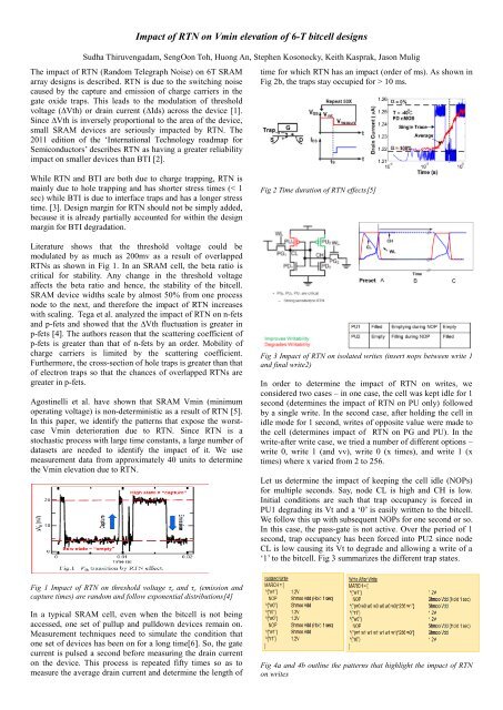
time for which <str<strong>on</strong>g>RTN</str<strong>on</strong>g> has an impact (order <str<strong>on</strong>g>of</str<strong>on</strong>g> ms). As shown in<br />
Fig 2b, the traps stay occupied for > 10 ms.<br />
While <str<strong>on</strong>g>RTN</str<strong>on</strong>g> and BTI are both due to charge trapping, <str<strong>on</strong>g>RTN</str<strong>on</strong>g> is<br />
mainly due to hole trapping and has shorter stress times (< 1<br />
sec) while BTI is due to interface traps and has a l<strong>on</strong>ger stress<br />
time. [3]. Design margin for <str<strong>on</strong>g>RTN</str<strong>on</strong>g> should not be simply added,<br />
because it is already partially accounted for within the design<br />
margin for BTI degradati<strong>on</strong>.<br />
Literature shows that the threshold voltage could be<br />
modulated by as much as 200mv as a result <str<strong>on</strong>g>of</str<strong>on</strong>g> overlapped<br />
<str<strong>on</strong>g>RTN</str<strong>on</strong>g>s as shown in Fig 1. In an SRAM cell, the beta ratio is<br />
critical for stability. Any change in the threshold voltage<br />
affects the beta ratio and hence, the stability <str<strong>on</strong>g>of</str<strong>on</strong>g> the <strong>bitcell</strong>.<br />
SRAM device widths scale by almost 50% from <strong>on</strong>e process<br />
node to the next, and therefore the impact <str<strong>on</strong>g>of</str<strong>on</strong>g> <str<strong>on</strong>g>RTN</str<strong>on</strong>g> increases<br />
with scaling. Tega et al. analyzed the impact <str<strong>on</strong>g>of</str<strong>on</strong>g> <str<strong>on</strong>g>RTN</str<strong>on</strong>g> <strong>on</strong> n-fets<br />
and p-fets and showed that the ∆Vth fluctuati<strong>on</strong> is greater in<br />
p-fets [4]. The authors reas<strong>on</strong> that the scattering coefficient <str<strong>on</strong>g>of</str<strong>on</strong>g><br />
p-fets is greater than that <str<strong>on</strong>g>of</str<strong>on</strong>g> n-fets by an order. Mobility <str<strong>on</strong>g>of</str<strong>on</strong>g><br />
charge carriers is limited by the scattering coefficient.<br />
Furthermore, the cross-secti<strong>on</strong> <str<strong>on</strong>g>of</str<strong>on</strong>g> hole traps is greater than that<br />
<str<strong>on</strong>g>of</str<strong>on</strong>g> electr<strong>on</strong> traps so that the chances <str<strong>on</strong>g>of</str<strong>on</strong>g> overlapped <str<strong>on</strong>g>RTN</str<strong>on</strong>g>s are<br />
greater in p-fets.<br />
Agostinelli et al. have shown that SRAM <strong>Vmin</strong> (minimum<br />
operating voltage) is n<strong>on</strong>-deterministic as a result <str<strong>on</strong>g>of</str<strong>on</strong>g> <str<strong>on</strong>g>RTN</str<strong>on</strong>g> [5].<br />
In this paper, we identify the patterns that expose the worstcase<br />
<strong>Vmin</strong> deteriorati<strong>on</strong> due to <str<strong>on</strong>g>RTN</str<strong>on</strong>g>. Since <str<strong>on</strong>g>RTN</str<strong>on</strong>g> is a<br />
stochastic process with large time c<strong>on</strong>stants, a large number <str<strong>on</strong>g>of</str<strong>on</strong>g><br />
datasets are needed to identify the impact <str<strong>on</strong>g>of</str<strong>on</strong>g> it. We use<br />
measurement data from approximately 40 units to determine<br />
the <strong>Vmin</strong> elevati<strong>on</strong> due to <str<strong>on</strong>g>RTN</str<strong>on</strong>g>.<br />
Fig 2 Time durati<strong>on</strong> <str<strong>on</strong>g>of</str<strong>on</strong>g> <str<strong>on</strong>g>RTN</str<strong>on</strong>g> effects[5]<br />
Fig 3 <str<strong>on</strong>g>Impact</str<strong>on</strong>g> <str<strong>on</strong>g>of</str<strong>on</strong>g> <str<strong>on</strong>g>RTN</str<strong>on</strong>g> <strong>on</strong> isolated writes (insert nops between write 1<br />
and final write2)<br />
In order to determine the impact <str<strong>on</strong>g>of</str<strong>on</strong>g> <str<strong>on</strong>g>RTN</str<strong>on</strong>g> <strong>on</strong> writes, we<br />
c<strong>on</strong>sidered two cases – in <strong>on</strong>e case, the cell was kept idle for 1<br />
sec<strong>on</strong>d (determines the impact <str<strong>on</strong>g>of</str<strong>on</strong>g> <str<strong>on</strong>g>RTN</str<strong>on</strong>g> <strong>on</strong> PU <strong>on</strong>ly) followed<br />
by a single write. In the sec<strong>on</strong>d case, after holding the cell in<br />
idle mode for 1 sec<strong>on</strong>d, writes <str<strong>on</strong>g>of</str<strong>on</strong>g> opposite value were made to<br />
the cell (determines impact <str<strong>on</strong>g>of</str<strong>on</strong>g> <str<strong>on</strong>g>RTN</str<strong>on</strong>g> <strong>on</strong> PG and PU). In the<br />
write-after write case, we tried a number <str<strong>on</strong>g>of</str<strong>on</strong>g> different opti<strong>on</strong>s –<br />
write 0, write 1 (and vv), write 0 (x times), and write 1 (x<br />
times) where x varied from 2 to 256.<br />
Let us determine the impact <str<strong>on</strong>g>of</str<strong>on</strong>g> keeping the cell idle (NOPs)<br />
for multiple sec<strong>on</strong>ds. Say, node CL is high and CH is low.<br />
Initial c<strong>on</strong>diti<strong>on</strong>s are such that trap occupancy is forced in<br />
PU1 degrading its Vt and a „0‟ is easily written to the <strong>bitcell</strong>.<br />
We follow this up with subsequent NOPs for <strong>on</strong>e sec<strong>on</strong>d or so.<br />
In this case, the pass-gate is not active. Over the period <str<strong>on</strong>g>of</str<strong>on</strong>g> 1<br />
sec<strong>on</strong>d, trap occupancy has been forced into PU2 since node<br />
CL is low causing its Vt to degrade and allowing a write <str<strong>on</strong>g>of</str<strong>on</strong>g> a<br />
„1‟ to the <strong>bitcell</strong>. Fig 3 summarizes the different trap states.<br />
Fig 1 <str<strong>on</strong>g>Impact</str<strong>on</strong>g> <str<strong>on</strong>g>of</str<strong>on</strong>g> <str<strong>on</strong>g>RTN</str<strong>on</strong>g> <strong>on</strong> threshold voltage τ e and τ c (emissi<strong>on</strong> and<br />
capture times) are random and follow exp<strong>on</strong>ential distributi<strong>on</strong>s[4]<br />
In a typical SRAM cell, even when the <strong>bitcell</strong> is not being<br />
accessed, <strong>on</strong>e set <str<strong>on</strong>g>of</str<strong>on</strong>g> pullup and pulldown devices remain <strong>on</strong>.<br />
Measurement techniques need to simulate the c<strong>on</strong>diti<strong>on</strong> that<br />
<strong>on</strong>e set <str<strong>on</strong>g>of</str<strong>on</strong>g> devices has been <strong>on</strong> for a l<strong>on</strong>g time[6]. So, the gate<br />
current is pulsed a sec<strong>on</strong>d before measuring the drain current<br />
<strong>on</strong> the device. This process is repeated fifty times so as to<br />
measure the average drain current and determine the length <str<strong>on</strong>g>of</str<strong>on</strong>g><br />
Fig 4a and 4b outline the patterns that highlight the impact <str<strong>on</strong>g>of</str<strong>on</strong>g> <str<strong>on</strong>g>RTN</str<strong>on</strong>g><br />
<strong>on</strong> writes
Next, we determine the impact <str<strong>on</strong>g>of</str<strong>on</strong>g> <str<strong>on</strong>g>RTN</str<strong>on</strong>g> when we follow the<br />
multiple NOPs with a write-after-write pattern to the <strong>bitcell</strong>.<br />
Initial c<strong>on</strong>diti<strong>on</strong>s are such that node “CH” is high and “CL” is<br />
low. PU2 has trap occupancy forced into it causing the Vt to<br />
be degraded thus allowing a write <str<strong>on</strong>g>of</str<strong>on</strong>g> a “0” (pulling CH low).<br />
When we do multiple write <str<strong>on</strong>g>of</str<strong>on</strong>g> „0s‟ to the <strong>bitcell</strong> PU1 is<br />
c<strong>on</strong>stantly exercised. Trap vacancy in PU1 improves its<br />
threshold voltage so that writing a “0” <strong>on</strong> node CL is much<br />
harder and could even fail. Finally, although the PG<br />
transistors are <strong>on</strong>ly turned <strong>on</strong> for a short durati<strong>on</strong> during<br />
SRAM cell access, sequential pulses <strong>on</strong> PG1 during writeafter-write<br />
access are sufficient to force trap occupancy in<br />
PG1 and degrade Twrite <str<strong>on</strong>g>of</str<strong>on</strong>g> the final operati<strong>on</strong>. Fig 4<br />
describes the isolated write and write-after-write patterns and<br />
the test algorithm used.<br />
Isolated<br />
Write<br />
T hold<br />
T write<br />
Preset A Hold Write A<br />
boundary]. The <strong>Vmin</strong> in the other cases was lower than it was<br />
for the write-after-write. It is comm<strong>on</strong>ly accepted that traps<br />
causing transistor degradati<strong>on</strong> due to <str<strong>on</strong>g>RTN</str<strong>on</strong>g> have a time<br />
c<strong>on</strong>stant within 1 sec while those due to BTI have a much<br />
l<strong>on</strong>ger time c<strong>on</strong>stant. Since all the test patterns we applied are<br />
for 1 sec or less, the effects we are characterizing are solely<br />
due to <str<strong>on</strong>g>RTN</str<strong>on</strong>g>.<br />
Fig 6a and 6b outline the basic patterns to determine the<br />
cause <str<strong>on</strong>g>of</str<strong>on</strong>g> the <strong>Vmin</strong> failure<br />
Write<br />
After<br />
Write<br />
T hold T relax T write<br />
Preset A Hold Write A Write A<br />
Fig 4c and 4d Patterns used to test impact <str<strong>on</strong>g>of</str<strong>on</strong>g> <str<strong>on</strong>g>RTN</str<strong>on</strong>g> <strong>on</strong> writes to the<br />
<strong>bitcell</strong><br />
The <strong>Vmin</strong> <str<strong>on</strong>g>of</str<strong>on</strong>g> a <strong>bitcell</strong> is the minimum operating voltage at<br />
which reads and writes occur. Due to <str<strong>on</strong>g>RTN</str<strong>on</strong>g>, we would observe<br />
elevated <strong>Vmin</strong>s following a write-after-write operati<strong>on</strong>.<br />
Successive WL pulses degrade reads and writes while read<br />
stability (ADM) improves as shown in Fig 5.<br />
Fig 5 <str<strong>on</strong>g>Impact</str<strong>on</strong>g> <str<strong>on</strong>g>of</str<strong>on</strong>g> <str<strong>on</strong>g>RTN</str<strong>on</strong>g> <strong>on</strong> write after write<br />
In order to test the impact <str<strong>on</strong>g>of</str<strong>on</strong>g> these patterns <strong>on</strong> the <strong>Vmin</strong> <str<strong>on</strong>g>of</str<strong>on</strong>g> the<br />
<strong>bitcell</strong>, we selected 40 units from 32nm silic<strong>on</strong> that had <strong>Vmin</strong><br />
failures due to SRAMs. These units had elevated <strong>Vmin</strong> at 0C<br />
versus 95C indicating that writes were the problem (Fig 9).<br />
BIST algorithms were run to identify the cause <str<strong>on</strong>g>of</str<strong>on</strong>g> <strong>Vmin</strong><br />
failures. A march algorithm c<strong>on</strong>sists <str<strong>on</strong>g>of</str<strong>on</strong>g> march lines, where<br />
each march line is comprised <str<strong>on</strong>g>of</str<strong>on</strong>g> read, write, or read/write<br />
combinati<strong>on</strong> called march elements. Each march line is<br />
denoted with a ^ or v to represent the address directi<strong>on</strong>. A<br />
march line is run to completi<strong>on</strong> at each address before moving<br />
to the next address. When all addresses in the specified macro<br />
have been tested, BIST will proceed to the next march line.<br />
The BIST algorithms used to identify the units with write<br />
<strong>Vmin</strong> fails are described in Fig 6.<br />
There are a number <str<strong>on</strong>g>of</str<strong>on</strong>g> patterns in our test suite that<br />
specifically look for issues that cause elevated <strong>Vmin</strong>, say<br />
marginal bits due to elevated c<strong>on</strong>tact resistance, higher IR<br />
drop, etc. For <str<strong>on</strong>g>RTN</str<strong>on</strong>g> we looked at trap characteristics and<br />
applied test vectors within a short period which is within the<br />
range <str<strong>on</strong>g>of</str<strong>on</strong>g> <str<strong>on</strong>g>RTN</str<strong>on</strong>g> trap time c<strong>on</strong>stant [1 sec<strong>on</strong>d being the<br />
Fig 7 Addressing mode used for <str<strong>on</strong>g>RTN</str<strong>on</strong>g><br />
Fig 7 shows an example <str<strong>on</strong>g>of</str<strong>on</strong>g> a 4-bit address used in an array<br />
with 4 rows and 4 columns per data bit slice (2 data bits<br />
shown). The effective addressing achieved by fast column and<br />
Fast Row is listed in Table 4.62. In fast column, the rows are<br />
held while traversing the columns. In fast row mode, the<br />
columns are held while traversing the rows. BIST testcases<br />
normally use fast-column addressing but that leads to passgates<br />
being turned <strong>on</strong> for the n<strong>on</strong>-selected columns. In order<br />
to avoid that, fast-row addressing was used which we felt gave<br />
a more accurate picture <str<strong>on</strong>g>of</str<strong>on</strong>g> the impact due to <str<strong>on</strong>g>RTN</str<strong>on</strong>g>.<br />
Fig 8 shows the shmoo (normalized voltage versus frequency)<br />
plots for two <str<strong>on</strong>g>of</str<strong>on</strong>g> the units where we can observe that the <str<strong>on</strong>g>RTN</str<strong>on</strong>g><br />
patterns have elevated <strong>Vmin</strong>. We can also see that the writeafter-write<br />
case has the highest <strong>Vmin</strong>.<br />
1.60<br />
1.56<br />
1.52<br />
1.48<br />
1.44<br />
1.40<br />
1.36<br />
1.32<br />
1.28<br />
1.24<br />
1.20<br />
1.16<br />
1.12<br />
1.08<br />
1.04<br />
1.00<br />
VDD<br />
Isolated<br />
Write -5C<br />
200<br />
800<br />
200<br />
WAW<br />
-5C<br />
800<br />
Writeability<br />
-5C<br />
200<br />
Frequency (MHz)<br />
800<br />
Readability<br />
-5C<br />
200<br />
800
1.60<br />
1.56<br />
1.52<br />
1.48<br />
1.44<br />
1.40<br />
1.36<br />
1.32<br />
1.28<br />
1.24<br />
1.20<br />
1.16<br />
1.12<br />
1.08<br />
1.04<br />
1.00<br />
VDD<br />
Isolated<br />
Write -5C<br />
200<br />
800<br />
200<br />
WAW<br />
-5C<br />
800<br />
Writeability<br />
-5C<br />
Readability<br />
-5C<br />
Frequency (MHz)<br />
Fig 8 <str<strong>on</strong>g>Impact</str<strong>on</strong>g> <str<strong>on</strong>g>of</str<strong>on</strong>g> <str<strong>on</strong>g>RTN</str<strong>on</strong>g> patterns <strong>on</strong> write <strong>Vmin</strong> (20-60mv elevati<strong>on</strong>) for<br />
2 units out <str<strong>on</strong>g>of</str<strong>on</strong>g> the 40 tested (ISO implies isolated write, waw implies<br />
write-after-write)<br />
The tests were repeated at both -5C and 71C. The write-afterwrite<br />
pattern showed an elevated <strong>Vmin</strong> at both temperatures<br />
as shown in Fig 9.<br />
200<br />
800<br />
200<br />
800<br />
1.750<br />
1.625<br />
1.500<br />
1.375<br />
1.250<br />
1.125<br />
1.000<br />
Fig 10 <str<strong>on</strong>g>Impact</str<strong>on</strong>g> <str<strong>on</strong>g>of</str<strong>on</strong>g> <str<strong>on</strong>g>RTN</str<strong>on</strong>g> <strong>on</strong> <strong>Vmin</strong> for 40 units (average) at 200Mhz<br />
In summary, we were able to successfully identify the <str<strong>on</strong>g>RTN</str<strong>on</strong>g><br />
testcases that impact the write <strong>Vmin</strong> <str<strong>on</strong>g>of</str<strong>on</strong>g> <strong>bitcell</strong>s . By applying<br />
these testcases to actual silic<strong>on</strong>, we were also able to show<br />
that <str<strong>on</strong>g>RTN</str<strong>on</strong>g> causes write <strong>Vmin</strong>s to be elevated by 20-60mv for<br />
write-after-write operati<strong>on</strong>s.<br />
REFERENCES<br />
[1] S.O. Toh et al., in IEDM Tech. Dig., pp. 767-770, 2009.<br />
[2] Internati<strong>on</strong>al Technology roadmap for<br />
Semic<strong>on</strong>ductors, 2011 Editi<strong>on</strong><br />
[3] T. Grasser et al, in IEDM Tech. Dig., pp. 729-732, 2009.<br />
[4] N. Tega et al, in IEDM Tech. Dig , pp. 491-494 ,2006<br />
[5] M. Agostinelli et al, in IEDM Tech Dig, pp. 655-658, 2005<br />
[6] S.O.Toh et al.,in Symp. VLSI Tech., pp. 204-205, 2011<br />
ACKNOWLEDGEMENTS<br />
The authors are grateful to Aar<strong>on</strong> Grenat, Andrew Kegel and<br />
other managers for allowing this research to c<strong>on</strong>clude<br />
successfully.<br />
1.750<br />
1.625<br />
1.500<br />
1.375<br />
1.250<br />
1.125<br />
1.000<br />
Fig 9 <str<strong>on</strong>g>Impact</str<strong>on</strong>g> <str<strong>on</strong>g>of</str<strong>on</strong>g> <str<strong>on</strong>g>RTN</str<strong>on</strong>g> tests <strong>on</strong> write <strong>Vmin</strong> at hot and cold for the<br />
above two units<br />
Fig 10 shows the average elevati<strong>on</strong> in <strong>Vmin</strong> due to writeafter-write<br />
<strong>on</strong> the 40 units tested.