SURFACE ANALYSIS OF MONO-CRYSTALLINE SILICON SOLAR ...
SURFACE ANALYSIS OF MONO-CRYSTALLINE SILICON SOLAR ...
SURFACE ANALYSIS OF MONO-CRYSTALLINE SILICON SOLAR ...

You also want an ePaper? Increase the reach of your titles
YUMPU automatically turns print PDFs into web optimized ePapers that Google loves.
<strong>SURFACE</strong> <strong>ANALYSIS</strong> <strong>OF</strong> <strong>MONO</strong>-<strong>CRYSTALLINE</strong> <strong>SILICON</strong> <strong>SOLAR</strong> CELLS FOR MANUFACTURING CONTROLM.J. Ariza and D.LeinenDepartamento de Física Aplicada I, Facultad de Ciencias, Universidad de Málaga, E-29071 Málaga, Spain., Phone: 34952131928,Fax: 34952132000, E-mail: dietmar@uma.esF. MartínDepartamento de Ingeniería Química, Facultad de Ciencias, Universidad de Málaga, E-29071 Málaga, Spain., Phone: 34952132037,Fax: 34952132000, E-mail: marjim@uma.esAbstract – X-ray photoelectron spectroscopy (XPS) has been applied to the surfaces of a silicon wafer in thedifferent steps of the assembly line for mono-crystalline silicon solar cell manufacturing. XPS results have shownthat, already at the textured mono-crystalline silicon surface a considerable amount of carbon is present. This amountdecreases slightly but is still present after the process of phosphor diffusion (p-n junction) as well as after posteriorcalcination in humid air for SiO 2 film formation (passivation). During the anti-reflection CVD coating process of aTiO 2 film, this amount of carbon may be buried. After calcination of the film in order to obtain the TiO 2 rutile phasean even higher amount of carbon is detected, in that case, at the TiO 2 surface indicating that not all organic parts fromthe tetra-isopropile orto-titanate (TPT) precursor have been released from the film. Furthermore, phosphor is foundat the rutile TiO 2 surface indicating an extra phosphor diffusion from the silicon bulk through the TiO 2 film up to itssurface. These results demonstrate how thermal treatments applied in a assembly line can influence and may changethe initially intended compositional distribution as well as introduce defects in the solar cell device.1. INTRODUCTIONMono-crystalline silicon is still the most common material usedfor manufacturing solar cells. The different steps and alltechniques applied in the assembly line of mono-crystallinesilicon solar cell manufacturing are now well established forabout two decades (Kelly, 1978; Selders and Bonnet, 1979). Atthe end of the manufacturing process each device is usuallysubjected to an efficiency test. Bad cells, i.e. which yield toosmall photo currents under standardised conditions, are excludedfor the assembly of the solar panel. This means a waste ofmoney and an increase of the price of the final product topurchase. The reason why some cells obtained in an identicalfabrication process yield a worse result than others is oftenunknown, but, in any case, must be related to defects whichinduce the recombination of the charge carriers before theircollection at the electrode. Those defects are in particularimportant at the interfaces as well as at the different surfacesexposed during the fabrication process of the solar cell device.Therefore XPS could be an adequate tool to get more inside tothis problem since it is a surface analysis technique which yieldscompositional and chemical information. However, mainlybecause of the matter of expense, this technique is not usuallyapplied for an analysis of real solar cell devices, neither of theend product as final device control nor of the device at itsdifferent fabrication steps. This is totally different to whathappens in basic research where materials intended to be usedfor solar cells have been investigated extensively by surfaceanalysis techniques. The main steps for manufacturing the solarcell device essentially are surface texturing in a humid acid line,phosphor diffusion (p-n junction) and surface oxidation(passivation) at about 1000ºC, anti-reflection coating (TiO 2 ) andcalcination to rutile at 850ºC, finger painting and firing of thefinal device at 973ºC, and the final device control (Cabello,1998).2. EXPERIMENTAL2.1 MaterialsMonocrystalline p(boron)-doped silicon grown in direction by the Czochralski method and cut in slices (wafers) of0.30 to 0.35 mm thickness have been used as source material forsolar cell manufacturing. The manufacturing process can beroughly separated in 6 successively following fabrication steps.After each step the wafer surface was studied by XPS andsample denomination was done as follows:sample 1: Si(111) textured surface, obtained after having passedthe humid line of cleaning, etching and surface neutralizationsample 2: after phosphor diffusion at about 1000ºC (formationof the p-n junction)sample 3: after SiO 2 passivation layer formation by calcinationin humid air at about 1000ºC
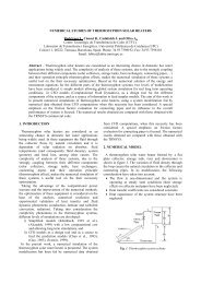
Figure 1: SEM pictures of two different textured silicon wafer surfaces
sample 4: after TiO 2 deposition (CVD) at 220ºCsample 5: after calcination in air at 850ºC for 20 min to obtainthe TiO 2 rutile phasesample 6: after serigraphic finger painting and contact formationby firing successively (assembly belt passing through variousfurnaces) to 220ºC, 240ºC, 464ºC and 973ºC, each for 7 s, anddirectly afterwards exposure and hence cooling down to ambienttemperature.For sample 6 we can distinguish two types of exposed surface,i.e. the photovoltaic active surface free of any metal deposition(sample 6a) and the part of the surface covered by the metallicfingers making the front contact of the solar cell device (sample6m). Front contact and back contact as well as back surface field(BSF) by Al doping has been done in the same fabrication step.In this contribution we refer only to the front side of the solarcell.2.2 Surface analysisDue to the short escape depth of photoelectrons (of the order of1 nm) analyzed in XPS (energy range: 0 to 1500 eV), XPS is anadequate tool to study surface effects originated during themanufacturing process of solar cell devices. With XPS allelements can be detected, unless H and He, whenever theconcentration of an element is above its detection limit. This isdependent on each electronic level of each element but roughlyof the order of 1% of all the atoms detected. In our case, XPSmeasurements were carried out with a PHI 5700 spectrometerequipment with Mg Kα radiation (1253.6 eV) and Al Kαradiation (1486.6 eV) as excitation sources. Multiregion spectrawere recorded at 45º take-off-angle with a concentrichemispherical energy electron analyzer operating in the constantpass energy mode at 29.35 eV, using a 380 µm diameter analysisarea. Under these conditions, the Au 4f 7/2 line was recorded with1.16 eV FWHM at a binding energy of 84.0 eV. Thespectrometer energy scale was calibrated using Cu 2p 3/2 , Ag3d 5/2 and Au 4f 7/2 photoelectron lines at 932.7, 368.3 and 84.0eV, respectively. The pressure in the analysis chamber wasmaintained lower than ∼10 -7 Pa. PHI ACCESS ESCA-V6.0 Fsoftware package was used for data acquisition and analysis.The atomic concentrations were calculated from thephotoelectron peak areas using Shirley background subtraction(Shirley, 1972) and sensitivity factors provided by thespectrometer manufacturer (PHI, 2000). Energy calibration wasdone with the C1s line at 284.6 eV. Peak fitting was performedwith Gaussian-Lorentzian bands.The morphological aspect of the wafer surface was studied by aJOEL JMS 6300 electron microscope. Information about theuniformity in height and size of the pyramids of the texturedsilicon surface was hereby obtained. Microanalysis (EDX) ofthe microscope could not be used as a comparative method forstudying the different layers on top of the silicon wafer due toits large information depth (various micrometers) far beyondany layer thickness as studied here (p-n junction at a depth ofabout 0.5 µm, SiO 2 passivation layer of about 60 nm, and TiO 2anti-reflection layer of about 30 nm) (Ariza, Leinen and Martin,2000).3. RESULTS3.1 Surface morphologyTexturing of the p-Si wafer surface increases the photovoltaicactive surface in about 25-30%. In this process, the initially flatsurface is transformed into a rough but regular surface formed bymicrometric pyramids of quadratic base and Si(111) faces. Thesize of these pyramids may vary approximately between 1 and10 µm as can be seen in Figure 1. It shows two SEM pictures oftwo different wafer surfaces, one with more or less uniformlybig pyramids and the other with a large amount of very smallpyramids between big ones. Due to the fact that the surface isrough but also regular and that the roughness determining size isin the range of µm, i.e. much beyond the thickness of the solarcell determining layers (n-Si, SiO 2 and TiO 2 ), each face of thepyramids includes the hole structure of the layer system.3.2 XPSFigure 2 shows the XPS survey spectra of the wafer surface atthe different steps of solar cell manufacturing, i.e. of sample 1 to6. As XPS is a surface sensitive technique by samplingphotoelectrons of discrete kinetic energy only from theuppermost atomic monolayers of a sample, equivalent to aninformation depth of about 10 to 20 nm, photoelectron andAuger peaks of Si and O are detected for sample 1 to 3 and of Tiand O for sample 4 to 6a due to the Si and SiO 2 surface and theTiO 2 surface respectively. The survey spectrum of sample 6mshows principally peaks of Ag and Pb from the top contact ofthe solar cell. Besides peaks of less intensity of P, C and Cl canbe seen in the survey spectra. Peaks of less intensity do notnecessarily mean that the corresponding element is found in lessconcentration at the sample surface but for atomic concentrationcalculations each peak must be weightened by a sensitivityfactor due to the X-ray excitation cross section of eachelectronic level of an element and a geometric factor dependingon the type of spectrometer. In Figure 3 high resolutionmutiregion spectra of the main signals, i.e. Si2p, Ti2p, O1s andC1s, are represented for the different sample surfaces. Table 1resumes the corresponding atomic concentrations calculatedfrom the photoelectron peak areas of all elements detected at thedifferent sample surfaces and the corresponding atomic ratios.As can be seen from Figure 3 and Table 1, the determiningelement
Intensity (a.u.)CKVVAgMVVTiLMMTiLMMSample 6mSample 6aOKLLAg3sPb4p3/2Ag3p1/2Ag3p3/2O1sTi2pPb4d3/2Pb4d5/2Ag3dC1sCl2sCl2pPb4fAg4sTi3sTi3pAg4dPb5dIntensity (a.u.)1000 800 600 400 200 0CKVVSample 5Sample 4TiLMMTiLMMOKLLTi2sO1sTi2pC1sP2sP2pTi3sTi3pO2s1000 800 600 400 200 0O1sCKVVSample 3OKLLC1sP2sSi2sP2pSi2pO2sIntensity (a.u.)Sample 2Sample 11000 800 600 BE (eV) 400 200 0Figure 2: XPS survey spectra of the different wafer surfaces
Table 1. Surface atomic concentration, and some ratios between them, for the different samples.Sample 1 Sample 2 Sample 3 Sample 4 Sample 5 Sample 6a Sample 6m%Ti --- --- --- 19.8 20.9 22.0 0.0%Si 59.8 32.0 29.1 2.4 0.5 0.6 4.8%O 29.8 59.2 63.6 50.3 54.9 57.8 22.3%C 9.6 4.3 5.4 27.2 20.2 21.1 33.7%P --- 4.5 1.9 0.3 3.6 1.1 0.0%Ag --- --- --- --- --- 0.2 15.3%Pb --- --- --- --- --- 0.3 7.0%Cl --- --- --- --- --- 0.0 16.9Ti/O --- --- --- 0.394 0.381 0.381 ---Si/O 2.007 0.541 0.458 0.048 0.009 0.010 ---Si/Ti --- --- --- 0.121 0.024 0.027 ---for sample 1 to 3 is Si and for sample 4 to 6a is Ti. Figure 4shows the Lorentzian-Gaussian type fitting curves (continuesline) to the recorded photoelectron spectra (points) due to thedifferent chemical environment of each element. In the followingwe will discuss the XPS results for each sample surface.4. DISCUSSION4.1 Sample 1 (the textured silicon surface)For sample 1, as can be seen in Figure 3 and Figure 4, we candistinguish two well separated Si2p peaks. The one at 99.4 eVin binding energy (BE) corresponds to the p-type silicon bulk(Hedman et. al., 1972) and the other at 103.2 eV to silicon oxide(Moulder, 1998), the latter indicating that the uppermost atomicmonolayer of the silicon wafer has been oxidized to SiO 2 due tobeing in contact with the atmosphere. Boron has not beendetected by XPS since its atomic concentration is below theXPS detection limit. Also about 10% of carbon (see Table 1 andFigure 3) has been detected at the silicon surface. A few min of 4KeV Ar + sputtering eliminates this amount of carbon showingthat it is a surface contamination due to the exposure of thesilicon wafer to air. In Figure 4, the C1s signal can be seendeconvoluted into different contributions. About 23% of thesignal is due to carbon in various environments with O and H.Fitting has been done with bands due to contributions of carbonoxygenfunctional groups (Desimoni et al., 1990). But the mainpeak of the C1s signal is due to C-C bindings givingcontributions at 284.6 eV in BE. Here, we would like to pointout that the presence of carbon at the silicon wafer surface couldbe an critical point for the further manufacturing steps,especially when heating processes are involved and the amountof carbon in spite of being desorbed and burned to CO 2 couldalso diffuse into the silicon bulk crystal structure and hencegenerate centers of recombination for charge carriers.4.2 Sample 2 (after phosphor diffusion)Besides the elements observed in sample 1, phosphor isdetected at the surface of sample 2 (see Table 1). Thisdemonstrates that P stays in excess at the wafer surface sincethe P doping concentration making the p-n junction in the siliconbulk is below XPS detection limit. Figure 4 shows the P 2p peakdeconvoluted into P 2p 3/2 and P 2p 1/2 contributions. The P 2p 3/2peak is found at 134.6 eV, a very high value in BE compared tovalues documented in the literature (Moulder et al., 1992). Thisshows that P at the waver surface is found in a veryelectronegative surrounding. However, Chlorine, an elementinvolved in the process of P diffusion (phosphor oxi-chloride ina nitrogen flux is used), has not been detected at the wafersurface. Only a very small N 1s signal has been detected yieldinga atomic ratio of N/Si=0.0089. On the other hand, the Si 2psignal has changed showing only one peak at 103.7 eV (see Fig.3) to be entirely due to SiO 2 which has been formed at the wafersurface during the P diffusion process at about 1000ºC.Correspondingly the amount of oxygen has increased to thedouble compared to sample 1 yielding a atomic ratio ofSi/O=0.54 near to 0.5 for SiO2. Also the
Si2pSample 1O1sSample 1Sample 1C1sSample 2Sample 2 Sample 2Intensity (a.u.)Sample 3 Sample 3107 104 101 98Ti2pSample 4Sample 4Sample 3Sample 4Sample 5Sample 5Sample 5Sample 6a468 464 460 456BE (eV)Sample 6a536 534 532 530 528BE (eV)Sample 6a291 288 285 282BE (eV)Figure 3: XPS Multiregion spectra of the different sample surfacesIntensity (a.u.)Intensity (a.u.)Si2pSample 1-- 99.4 eV103.2 eV --103.5 eV --Sample 3107 103 99P2pSample 5134.6 eV --133.5 eV --Sample 3Ti2pSample 5467 462 457O1sSample 5p 1/2p 3/2-- 532.4 eV 532.7 eV --532.0 eV ---- 530.9 eV458.4 eV --Sample 1Sample 3529.5 eV --C1sSample 1Sample 3Sample 5-- 288.5 eV-- 287.3 eV-- 286.1 eV284.6 eV --138 134 130BE (eV)536 532 528BE (eV)290 286 282BE (eV)Figure 4: Fitting of the photoelectron peaks Si 2p, Ti 2p, P 2p, O 1s and C 1s of sample 1,3 and 5.
O1s peak has shifted to a higher binding energy of 532.2 eV.Furthermore the carbon amount has decreased to the half butshowing a C 1s peak of similar contributions as in sample 1 (seeFigure 3).4.3 Sample 3 (after surface passivation)The thermal treatment at about 1000ºC in humid air ensures thatall silicon atoms in a surface layer of about 50 nm thickness areoxidized to SiO 2 . This can be seen in Table 1 which shows anincrease in O concentration and Figure 4 which shows the Si 2pand O 1s signal at 103.5 eV and 532.7 eV respectively, typicalfor SiO 2 (Moulder et al. 1992). The Si/O ratio (Table 1) staysbelow 0.5 because some oxygen is in the C-O bindings of thecarbon surface contamination which stays approximatelyconstant compared to sample 2. On the other hand, the Pconcentration at the wafer surface has diminished to about thehalf compared to sample 2 due to evaporation and probably outdiffusionduring the elevated temperature.4.4 Sample 4 (after TiO 2 deposition by CVD at 220ºC)The wafer surface has been changed in this fabrication step to anamorphous TiO 2 surface. The atomic concentration of sample 4given in Table 1 shows that besides Ti and O a huge amount ofcarbon is detected at the sample surface. This indicates that notall organic parts from the TPT precursor have been released inthe CVD process at 220ºC from the film. The Ti 2p 3/2 peak andO 1s peak are found at 458.2 eV and 529.6 eV (see Figure 3)slightly below the values of 458.5 eV and 529.9 eV given inliterature for amorphous TiO 2 (Moulder et al., 1992). The lattermight be due to somewhat incorrect energy calibration whenputting the C 1s signal to 284.6 eV. Probably, a value of 285.0eV would be more correct taking into account the maincontribution in the C 1s signal due to aliphatic carbon. On theother hand, in the C 1s region we can observe a newcontribution, a small peak, at about 289 eV which indicates theincorporation of carbonate species in the film (Desimoni et al.1990) which have been formed during the film deposition.Nitrogen used as driving gas for the TPT precursor has beendetected in very small amount giving a atomic ratio of N/Ti =0.086. This nitrogen might be buried during deposition in theTiO2 film. Table 1 shows that Si is still detected by XPS in ∼2.4 atom % due to the fact that the deposited TiO 2 film isrelatively thin (∼30 nm thick). Furthermore even P is found invery low concentration indicating diffusion and segregation ofthis element to the TiO 2 surface during the film deposition at220ºC. The deconvolution of the O 1s signal (not shown inFigure 4 for sample 4) indicates that about 20 % of the totalamount of O detected by XPS is due to bindings of O to C andof O to Si (the latter due to the SiO 2 layer of the substrate). Thisexplains the Ti/O ratio below 0.5 for TiO 2 given in Table 1.4.5 Sample 5 (after calcination in air at 850ºC)Calcination of the TiO 2 film in air leads to the TiO 2 rutile crystalphase. The calcination process also changes the atomicconcentration values at the TiO 2 film surface as can be seen inTable 1. The Si concentration has dropped to 0.5 atom %indicating that the TiO 2 anti-reflection coating has changed to amore compact and uniform film coverage. This can also be seenby the peak narrowing of the Ti 2p signal due to well definedelectronic levels in the rutile crystal phase. Furthermore, Table 1shows that although the carbon amount has dropped to about 20atom % it is still high, i.e. similar to the amount of detected Tiatoms at the film surface. This shows that not all organic partshave been burned to CO 2 and have been released from the TiO 2film during its crystallization although the calcination time hasbeen considerably long (20 min). The C 1s peak (see Figure 4)shows still contributions due to C-O bindings of the differentcarbon-oxygen functional groups including carbonates.Correspondingly the O 1s peak has been deconvoluted into thecontributions of O in TiO 2 (fitting band at 529.5 eV) and O inC-O bindings. Taking into account the O 1s band at 529.5 eV forthe Ti/O ratio calculation it yields a value of 0.52 in reasonableagreement with the theoretical value of 0.5 for TiO 2 and thusjustifying, on the other hand, the fitting procedure. Furthermore,an important effect of the calcination process has been thestrong increase of P concentration to about 3.6 atom % (increaseby a factor of 7 compared to sample 4) which clearly shows thatcalcination during 20 min at 850ºC has given enough time andenergy to let diffuse P atoms to the surface and hence mostprobably also to redistribute P atoms and thus the Pconcentration in the Si bulk. We would like to point out that thiscould affect the position in depth and the range of the p-njunction in the solar cell device. At the TiO 2 surface the P 2p 3/2peak is found at 133.5 eV, i.e. somewhat lower than in sample 3(see Figure 4). Also nitrogen has been detected but in even lowerconcentration as before calcination (N/Ti = 0.025). Finally, theTi 2p 3/2 peak at 458.4 eV and the corresponding O 1s band at529.5 eV have been found again at somewhat lower values thangiven for rutile TiO 2 (i.e. 459.2 eV and 529.9 eV) as given in theliterature (Moulder et al., 1992) probably also due to the bindingenergy calibration procedure as mentioned before in section 4.4.4.6 Sample 6a (the photovoltaic active wafer surface after fingerpainting and firing to 973ºC)The main features of this surface are similar to those of sample5. In principal, the surface should not have altered since XPSanalysis has been made in this case far away from the zones ofthe metallic contact (fingers). However, since the process formaking the front contact involves again a heating process,although short in time compared to the calcination processperformed before, it is of interest to study the surface again. InFigure 3 we can observe that the main peaks in form andintensity due to Ti, O and C and thus the corresponding atomicconcentrations (see Table 1) have practically not changedcompared to sample 5. However, differences can be found dueto elements in minor concentration. For example, the Pconcentration has diminished considerably and the P 2p 3/2 peakhas shifted again to a higher BE of 134.0 eV indicating once againa redistribution of this element which seems to move easily inthese materials. Furthermore, Ag and Pb are detected in smallconcentration although far away from the metallic deposits ofthe front contact. This indicates that apart from an in-depth
diffusion of the metal elements for solar cell device top contactmaking, those elements diffuse laterally in the surface of theTiO 2 film.4.6 Sample 6m (the surface of the metallic finger after fingerpainting and firing to 973ºC)As we can see in Table 1, the metallic deposits in form of fingerson the front side of the solar cell contain various elements. Ag isthe metallic element for making the front contact, showing a Ag3d 5/2 peak at 368.1 eV typical for metallic silver. But also otherelements in even higher concentration as C, O, Cl, Pb and someSi are found at the front contact surface. Among those C is themost abundant element at the finger surface. The C 1s signal(not shown here) shows that about 10 % of its total intensityare due to carbonate species. Also the Pb 4f 7/2 peak, found at138.8 eV, corresponds to lead oxide. All this demonstrates thatduring the firing process, the organic parts of the paste used forserigraphic finger painting not have been eliminated forcompletely.5. CONCLUSIONSHedman J., Bear Y., Berndtson A., Klasson M., Leonhardt G.,Nilsson R., Nordling C. (1972) J. Electron Spectrosc. Phenom.1, 101Kelly H. (1978). Photovoltaic Power Systems: A Tour throughthe Alternatives, Science 199,634Moulder J.F., Stickle W.F., Sobol P.E., Bomben K.D. (1992), inHandbook of X-ray Photoelectron Spectroscopy. Ed.by J.Chastain. Published by PHI, 1992PHI (2000), Physical Electronics, 6509 Flying Cloud Drive,Eden Prairie, Mn 55344, USA.Selders M. and Bonnet D. (1979). Solarzellen, Physik in unsererZeit 10, 3-16Shirley DA. (1972) Phys. Rev. B 5, 4709.This study has shown that XPS can be applied successfully tothe study of very rough sample surfaces as those of texturedsilicon wafers for the control of the manufacturing process ofmono-crystalline silicon solar cells. XPS results have shown thatcarbon has been found at all wafer surfaces in the different stepsof solar cell manufacturing, i.e. as surface contamination on thetextured silicon wafer and, in higher concentrations, on the finalsolar cell device, both in the TiO 2 anti-reflection coating as wellas in the metallic fingers of the front contact. This shows that inthose fabrication steps where organic substances are involved(anti-reflection coating and finger painting) not all organic partshave been released during the thermal processes. On the otherhand, carbon from the silicon wafer surface could be buried inthe TiO 2 coating step and diffuse as well as carbon from theTiO 2 film into the silicon bulk and thus generating defects forcharge carrier recombination. Furthermore, we have seen that thephosphor concentration and distribution is very sensible on anythermal process which could therefore affect the n-doping leveland the depth of the p-n junction of the solar cell device.REFERENCESAriza M.J., Leinen D. and Martin F. (2000). A comparativechemical study of the top layers of two different quality siliconsolar cells, other contribution to EUROSUN2000Cabello Berdun S., personal communication. At that timeDirector of IS<strong>OF</strong>OTON (solar cell manufacturing industry),Malaga, Spain.Desimoni E., Casella G.I., Morone A. and Salvi A.M. (1990).XPS Determination of Oxygen-containing Functional Groups onCarbon-fiber Surfaces and Cleaning of These Surfaces, Surfaceand Interface Analysis 15, 627-634