SURFACE ANALYSIS OF MONO-CRYSTALLINE SILICON SOLAR ...
SURFACE ANALYSIS OF MONO-CRYSTALLINE SILICON SOLAR ...
SURFACE ANALYSIS OF MONO-CRYSTALLINE SILICON SOLAR ...

Create successful ePaper yourself
Turn your PDF publications into a flip-book with our unique Google optimized e-Paper software.
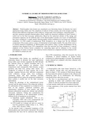
O1s peak has shifted to a higher binding energy of 532.2 eV.Furthermore the carbon amount has decreased to the half butshowing a C 1s peak of similar contributions as in sample 1 (seeFigure 3).4.3 Sample 3 (after surface passivation)The thermal treatment at about 1000ºC in humid air ensures thatall silicon atoms in a surface layer of about 50 nm thickness areoxidized to SiO 2 . This can be seen in Table 1 which shows anincrease in O concentration and Figure 4 which shows the Si 2pand O 1s signal at 103.5 eV and 532.7 eV respectively, typicalfor SiO 2 (Moulder et al. 1992). The Si/O ratio (Table 1) staysbelow 0.5 because some oxygen is in the C-O bindings of thecarbon surface contamination which stays approximatelyconstant compared to sample 2. On the other hand, the Pconcentration at the wafer surface has diminished to about thehalf compared to sample 2 due to evaporation and probably outdiffusionduring the elevated temperature.4.4 Sample 4 (after TiO 2 deposition by CVD at 220ºC)The wafer surface has been changed in this fabrication step to anamorphous TiO 2 surface. The atomic concentration of sample 4given in Table 1 shows that besides Ti and O a huge amount ofcarbon is detected at the sample surface. This indicates that notall organic parts from the TPT precursor have been released inthe CVD process at 220ºC from the film. The Ti 2p 3/2 peak andO 1s peak are found at 458.2 eV and 529.6 eV (see Figure 3)slightly below the values of 458.5 eV and 529.9 eV given inliterature for amorphous TiO 2 (Moulder et al., 1992). The lattermight be due to somewhat incorrect energy calibration whenputting the C 1s signal to 284.6 eV. Probably, a value of 285.0eV would be more correct taking into account the maincontribution in the C 1s signal due to aliphatic carbon. On theother hand, in the C 1s region we can observe a newcontribution, a small peak, at about 289 eV which indicates theincorporation of carbonate species in the film (Desimoni et al.1990) which have been formed during the film deposition.Nitrogen used as driving gas for the TPT precursor has beendetected in very small amount giving a atomic ratio of N/Ti =0.086. This nitrogen might be buried during deposition in theTiO2 film. Table 1 shows that Si is still detected by XPS in ∼2.4 atom % due to the fact that the deposited TiO 2 film isrelatively thin (∼30 nm thick). Furthermore even P is found invery low concentration indicating diffusion and segregation ofthis element to the TiO 2 surface during the film deposition at220ºC. The deconvolution of the O 1s signal (not shown inFigure 4 for sample 4) indicates that about 20 % of the totalamount of O detected by XPS is due to bindings of O to C andof O to Si (the latter due to the SiO 2 layer of the substrate). Thisexplains the Ti/O ratio below 0.5 for TiO 2 given in Table 1.4.5 Sample 5 (after calcination in air at 850ºC)Calcination of the TiO 2 film in air leads to the TiO 2 rutile crystalphase. The calcination process also changes the atomicconcentration values at the TiO 2 film surface as can be seen inTable 1. The Si concentration has dropped to 0.5 atom %indicating that the TiO 2 anti-reflection coating has changed to amore compact and uniform film coverage. This can also be seenby the peak narrowing of the Ti 2p signal due to well definedelectronic levels in the rutile crystal phase. Furthermore, Table 1shows that although the carbon amount has dropped to about 20atom % it is still high, i.e. similar to the amount of detected Tiatoms at the film surface. This shows that not all organic partshave been burned to CO 2 and have been released from the TiO 2film during its crystallization although the calcination time hasbeen considerably long (20 min). The C 1s peak (see Figure 4)shows still contributions due to C-O bindings of the differentcarbon-oxygen functional groups including carbonates.Correspondingly the O 1s peak has been deconvoluted into thecontributions of O in TiO 2 (fitting band at 529.5 eV) and O inC-O bindings. Taking into account the O 1s band at 529.5 eV forthe Ti/O ratio calculation it yields a value of 0.52 in reasonableagreement with the theoretical value of 0.5 for TiO 2 and thusjustifying, on the other hand, the fitting procedure. Furthermore,an important effect of the calcination process has been thestrong increase of P concentration to about 3.6 atom % (increaseby a factor of 7 compared to sample 4) which clearly shows thatcalcination during 20 min at 850ºC has given enough time andenergy to let diffuse P atoms to the surface and hence mostprobably also to redistribute P atoms and thus the Pconcentration in the Si bulk. We would like to point out that thiscould affect the position in depth and the range of the p-njunction in the solar cell device. At the TiO 2 surface the P 2p 3/2peak is found at 133.5 eV, i.e. somewhat lower than in sample 3(see Figure 4). Also nitrogen has been detected but in even lowerconcentration as before calcination (N/Ti = 0.025). Finally, theTi 2p 3/2 peak at 458.4 eV and the corresponding O 1s band at529.5 eV have been found again at somewhat lower values thangiven for rutile TiO 2 (i.e. 459.2 eV and 529.9 eV) as given in theliterature (Moulder et al., 1992) probably also due to the bindingenergy calibration procedure as mentioned before in section 4.4.4.6 Sample 6a (the photovoltaic active wafer surface after fingerpainting and firing to 973ºC)The main features of this surface are similar to those of sample5. In principal, the surface should not have altered since XPSanalysis has been made in this case far away from the zones ofthe metallic contact (fingers). However, since the process formaking the front contact involves again a heating process,although short in time compared to the calcination processperformed before, it is of interest to study the surface again. InFigure 3 we can observe that the main peaks in form andintensity due to Ti, O and C and thus the corresponding atomicconcentrations (see Table 1) have practically not changedcompared to sample 5. However, differences can be found dueto elements in minor concentration. For example, the Pconcentration has diminished considerably and the P 2p 3/2 peakhas shifted again to a higher BE of 134.0 eV indicating once againa redistribution of this element which seems to move easily inthese materials. Furthermore, Ag and Pb are detected in smallconcentration although far away from the metallic deposits ofthe front contact. This indicates that apart from an in-depth