Octal 3-State Noninverting Buffer/Line Driver/ Line ... - Datasheets
Octal 3-State Noninverting Buffer/Line Driver/ Line ... - Datasheets
Octal 3-State Noninverting Buffer/Line Driver/ Line ... - Datasheets

You also want an ePaper? Increase the reach of your titles
YUMPU automatically turns print PDFs into web optimized ePapers that Google loves.
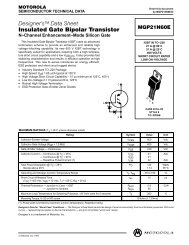
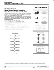
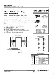
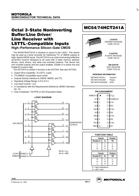
SEMICONDUCTOR TECHNICAL DATA High–Performance Silicon–Gate CMOSThe MC54/74HCT241A is identical in pinout to the LS241. This devicemay be used as a level converter for interfacing TTL or NMOS outputs toHigh–Speed CMOS inputs. The HCT241A is an octal noninverting buffer/linedriver/line receiver designed to be used with 3–state memory addressdrivers, clock drivers, and other bus–oriented systems. The device hasnon–inverted outputs and two output enables. Enable A is active–low andEnable B is active–high.The HCT241A is similar in function to the HCT244. See also HCT240.• Output Drive Capability: 15 LSTTL Loads• TTL/NMOS–Compatible Input Levels• Outputs Directly Interface to CMOS, NMOS, and TTL• Operating Voltage Range: 4.5 to 5.5 V• Low Input Current: 1 µA• In Compliance with the Requirements Defined by JEDEC StandardNo. 7A• Chip Complexity: 118 FETs or 29.5 Equivalent Gates202011201PIN ASSIGNMENTN SUFFIXPLASTIC PACKAGECASE 738–03DW SUFFIXSOIC PACKAGECASE 751D–04ORDERING INFORMATIONMC54HCTXXXAJMC74HCTXXXANMC74HCTXXXADWJ SUFFIXCERAMIC PACKAGECASE 732–03CeramicPlasticSOICLOGIC DIAGRAMENABLE AA1122019VCCENABLE BA1A22 18416YA1YA2YB4 3A2 4YB3 5181716YA1B4YA2A3614YA3A3YB2671514B3YA3DATA INPUTSA4B1811129YA4YB1NONINVERTINGOUTPUTSA4YB1GND8910131211B2YA4B1OUTPUTENABLESB2B31315B4 17ENABLE AENABLE B119753YB2YB3YB4PIN 20 = VCCPIN 10 = GNDFUNCTION TABLEInputsOutputEnable A A YAL L LL H HH X ZInputsOutputEnable B B YBH L LH H HL X ZZ = high impedanceX = don’t care10/95© Motorola, Inc. 19951 REV 6
MC54/74HCT241AÎÎÎÎÎÎÎÎÎÎÎÎÎÎÎÎÎÎÎÎÎÎÎMAXIMUM RATINGS*SymbolVCCParameterDC Supply Voltage (Referenced to GND)Value– 0.5 to + 7.0ÎÎÎÎÎÎÎÎÎÎÎÎÎÎÎÎÎÎÎÎÎÎÎÎÎÎÎÎÎÎÎÎÎÎÎÎÎÎÎÎÎÎÎÎÎÎÎÎÎÎÎÎÎÎÎÎÎÎÎÎÎÎÎÎÎÎÎÎÎV inVoutI inDC Input Voltage (Referenced to GND)DC Output Voltage (Referenced to GND)DC Input Current, per Pin– 1.5 to VCC + 1.5– 0.5 to VCC + 0.5ÎÎÎÎÎÎÎÎÎÎÎÎÎÎÎÎÎÎÎÎÎÎÎÎÎÎÎÎÎÎÎÎÎÎÎÎÎÎÎÎÎÎÎÎÎÎÎÎÎÎÎÎÎÎÎÎÎÎÎÎÎÎÎÎÎÎÎÎÎÎÎÎI outI CCP DDC Output Current, per PinDC Supply Current, VCC and GND PinsPower Dissipation in Still Air, Plastic or Ceramic DIP†SOIC Package†ÎÎÎÎÎÎÎÎÎÎÎÎÎÎÎÎÎÎÎÎÎÎÎÎÎÎÎÎÎÎÎÎÎÎÎÎÎÎÎÎÎÎÎÎÎÎÎÎÎÎÎÎÎÎÎÎÎÎÎÎÎÎÎÎÎÎÎÎÎÎÎÎT stgTLStorage TemperatureLead Temperature, 1 mm from Case for 10 Seconds(Plastic DIP or SOIC Package)(Ceramic DIP)ÎÎÎÎÎÎÎÎÎÎÎÎÎÎÎÎÎÎÎÎÎÎÎÎÎÎÎÎÎÎÎÎÎÎÎÎÎÎÎÎÎÎÎÎÎÎÎÎÎÎÎÎÎ ÎÎÎÎÎÎÎÎÎÎÎÎÎÎÎÎÎÎÎÎÎÎα20±35±75750500– 65 to + 150ÎÎÎÎÎÎÎÎÎÎÎÎÎÎÎÎÎÎÎÎÎÎÎÎ260300* Maximum Ratings are those values beyond which damage to the device may occur.Functional operation should be restricted to the Recommended Operating Conditions.†Derating — Plastic DIP: – 10 mW/ C from 65 to 125 CCeramic DIP: – 10 mW/ C from 100 to 125 CSOIC Package: – 7 mW/ C from 65 to 125 CÎÎÎÎÎÎÎÎÎÎÎÎÎÎÎÎÎÎÎÎFor high frequency or heavy load considerations, see Chapter 2 of the Motorola High–Speed CMOS Data Book (DL129/D).RECOMMENDED OPERATING CONDITIONSVCC DC Supply Voltage (Referenced to GND)4.5 5.5 VSymbolParameterMin Max UnitÎÎÎÎÎÎÎÎÎÎÎÎÎÎÎÎÎÎÎÎÎÎ ÎÎÎÎÎÎÎÎÎÎÎÎÎÎÎÎÎÎÎÎÎÎÎÎÎÎÎÎÎÎÎÎÎÎÎÎÎÎÎÎÎÎÎÎÎÎÎÎÎÎÎÎÎÎÎÎÎVin, Vout DC Input Voltage, Output Voltage (Referenced to GND) 0 ÎÎÎÎÎÎÎÎÎÎÎÎÎÎÎÎÎÎÎÎÎÎÎÎÎÎÎVCCVTAOperating Temperature, All Package Types– 55 + 125 CÎÎÎÎÎÎÎÎÎÎÎÎÎÎÎÎÎÎÎÎÎÎÎÎÎInput Rise and Fall Time (Figure 1)0 ÎÎÎÎÎÎÎÎÎÎÎÎÎÎÎÎÎÎÎÎ500nsÎÎÎÎÎÎÎÎÎÎÎÎÎÎÎÎÎtr, tfÎÎÎÎÎÎÎÎÎÎÎÎÎÎDC ELECTRICAL CHARACTERISTICS (Voltages Referenced to GND)ÎÎÎÎÎÎÎÎÎÎÎÎÎÎÎÎÎÎÎÎÎÎÎÎÎÎÎÎÎÎÎÎÎÎÎÎÎÎÎÎÎÎÎÎÎÎÎÎÎÎÎÎÎÎÎÎSymbolÎÎÎÎÎÎÎÎÎParameterÎÎÎÎTestÎÎÎÎÎÎÎÎÎÎÎÎÎÎÎÎÎÎÎÎÎConditionsÎÎÎUnitÎÎÎÎÎÎÎÎÎÎÎÎÎÎÎÎÎÎÎÎÎÎÎÎÎÎÎÎÎÎÎÎÎVIHVILVOHMinimum High–Level InputVoltageMaximum Low–Level InputVoltageMinimum High–Level OutputVoltageVout = 0.1 V or VCC – 0.1 V|Iout| 20 µAVout = 0.1 V or VCC – 0.1 V|Iout| 20 µAVin = VIH or VIL|Iout| 20 µAUnitVVVmAmAmAmWCCVCCV– 55 to25 CGuaranteed Limit 85 C 125 CÎÎÎÎÎÎÎÎÎÎÎÎÎÎÎÎÎÎÎÎÎÎÎ ÎÎÎÎÎÎÎÎÎÎÎÎÎÎÎÎÎÎÎÎÎÎÎÎÎÎÎÎÎ ÎÎÎÎÎÎÎÎÎÎÎÎÎÎÎÎÎÎÎÎÎÎÎÎÎÎÎÎÎÎÎÎÎÎÎÎÎÎÎÎÎÎÎÎÎÎÎÎÎÎÎÎÎÎÎÎÎÎÎVOLMaximum Low–Level OutputVoltageVin = VIH or VIL|Iout| 6 mAVin = VIH or VIL|Iout| 20 µAÎÎÎÎÎÎÎÎÎÎÎÎÎ ÎÎÎÎÎÎÎÎÎÎÎÎÎÎÎÎÎÎÎ ÎÎÎÎÎÎÎÎÎÎÎÎÎÎÎÎÎÎÎÎ ÎÎÎÎÎÎÎÎÎÎÎÎÎÎÎÎÎÎÎÎÎÎÎÎÎÎÎÎÎÎÎÎÎÎÎÎÎÎÎÎÎÎÎÎÎÎÎÎÎÎÎÎÎÎÎÎÎÎÎIinMaximum Input Leakage CurrentVin = VIH or VIL|Iout| 6 mAVin = VCC or GND4.55.54.55.54.55.52 20.80.82 20.80.84.4ÎÎÎÎ4.45.4 5.43.98 3.840.1ÎÎÎÎ0.10.1 0.10.26 0.33ÎÎÎÎÎÎÎÎÎÎÎÎÎÎÎÎÎÎÎ ÎÎÎÎÎÎÎÎÎÎÎÎÎÎÎÎÎÎÎÎÎÎÎÎÎÎÎÎÎÎÎÎ ÎÎÎÎÎÎÎÎÎÎÎÎÎÎÎÎÎÎÎ ÎÎÎÎÎÎÎÎÎÎÎÎÎÎÎÎÎÎÎÎÎÎÎÎÎÎÎÎÎÎÎÎÎÎÎÎÎÎÎÎIOZMaximum Three–<strong>State</strong>Leakage CurrentOutput in High–Impedance <strong>State</strong>Vin = VIL or VIHVout = VCC or GNDÎÎÎÎÎÎÎÎÎÎÎÎÎÎÎÎÎÎÎÎÎÎÎÎÎÎÎÎÎÎÎÎ ÎÎÎÎÎÎÎÎÎÎÎÎÎÎÎÎÎÎÎÎ ÎÎÎÎÎÎÎÎÎÎÎÎÎÎÎÎÎÎÎÎÎÎÎÎÎÎÎMaximum Quiescent SupplyÎÎÎÎÎÎÎÎÎVin = VCC or GNDÎÎÎÎ5.5ÎÎÎ4ÎÎÎÎÎÎÎÎ40ÎÎÎÎÎÎÎÎÎÎ160ÎÎεAICCCurrent (per Package)Iout = 0 µA4.54.55.54.55.55.5±0.1±0.5This device contains protectioncircuitry to guard against damagedue to high static voltages or electricfields. However, precautions mustbe taken to avoid applications of anyvoltage higher than maximum ratedvoltages to this high–impedance circuit.For proper operation, Vin andVout should be constrained to therange GND (Vin or Vout) VCC.Unused inputs must always betied to an appropriate logic voltagelevel (e.g., either GND or VCC).Unused outputs must be left open.±1.0±5.02 20 80.84.45.43.70.10.10.4±1.0±10VVVVµAµAÎÎÎÎÎÎÎÎÎÎÎÎÎÎÎÎÎÎÎÎÎÎÎÎÎÎÎÎÎÎÎÎÎÎÎÎÎÎÎÎÎÎÎÎÎÎÎÎÎÎÎÎÎÎÎÎÎÎÎÎÎÎÎÎÎ ÎÎÎÎÎÎÎÎÎÎÎÎÎÎÎÎÎÎÎÎÎÎÎÎÎÎMOTOROLA2High–Speed CMOS Logic DataDL129 — Rev 6
MC54/74HCT241AÎÎÎÎÎÎÎÎÎ ÎÎÎÎÎÎÎÎÎÎÎÎÎÎÎÎÎÎÎÎÎÎÎÎÎÎ∆ICCAdditional Quiescent SupplyCurrentVin = 2.4 V, Any One InputVin = VCC or GND, Other InputsÎÎÎÎÎÎÎÎÎÎÎÎÎÎÎÎÎÎÎÎÎÎ ÎÎÎÎÎÎÎÎÎÎÎÎÎÎÎÎÎÎÎÎÎÎÎÎÎÎÎÎÎÎÎÎÎÎÎÎÎÎÎlout =ÎÎÎÎÎÎÎÎÎÎÎÎÎÎÎÎÎÎÎÎÎÎÎÎÎÎ ÎÎÎÎ0 µAÎÎÎÎÎÎÎÎÎÎÎÎÎÎÎÎÎÎÎÎÎÎ5.5≥ –55 C2.925 C to 125 CNOTES:1. Information on typical parametric values along with frequency or heavy load considerations can be found in Chapter 2 of the Motorola High–Speed CMOS Data Book (DL129/D).2. Total Supply Current = ICC + Σ∆ICC.2.4mAÎÎÎÎÎÎÎÎÎÎÎÎÎÎÎÎÎÎÎÎÎÎÎÎÎÎÎÎÎÎÎÎÎHigh–Speed CMOS Logic DataDL129 — Rev 63 MOTOROLA
MC54/74HCT241AAC ELECTRICAL CHARACTERISTICS (VCC = 5.0 V ± 10%, CL = 50 pF, Input tr = tf = 6 ns)ÎÎÎÎÎÎÎÎÎÎÎÎÎÎÎÎÎÎÎÎÎÎÎÎÎÎÎÎÎÎÎÎÎÎÎÎÎÎÎÎÎÎÎÎÎÎÎÎÎÎÎÎÎÎÎÎÎÎÎÎÎÎÎÎÎÎÎÎÎÎÎÎÎÎÎÎÎÎÎÎÎÎÎÎÎÎÎÎÎÎÎÎÎÎÎÎÎÎÎÎÎÎÎÎÎSymbolParameter– 55 to25 CGuaranteed Limit 85 C 125 CÎÎÎÎÎÎÎÎÎÎÎÎÎÎÎÎÎÎÎÎÎÎÎÎÎÎÎÎÎÎÎÎÎÎÎÎÎÎtPLH, Maximum Propagation Delay, A to YA or B to YB23 29 35 nstPHL(Figures 1 and 3)UnitÎÎÎÎÎÎÎÎÎÎÎÎÎÎÎÎÎÎÎÎÎÎÎÎÎÎÎÎÎÎÎÎÎÎtPLZ,ÎÎÎÎÎÎÎÎMaximum Propagation Delay, Output Enable to YA or YBÎÎÎÎÎÎÎÎÎÎÎÎÎÎÎÎÎÎÎÎÎÎÎÎÎÎÎÎÎÎÎÎÎÎÎÎÎÎ30ÎÎÎÎÎÎÎÎ38ÎÎÎÎÎÎÎÎ45ÎÎÎÎÎÎÎÎnsÎÎÎÎÎÎtPHZ(Figures 2 and 4)tPZL,ÎÎÎÎMaximum Propagation Delay, Output Enable to YA or YBÎÎÎÎÎÎÎÎÎÎÎÎÎÎÎÎÎÎÎ26ÎÎÎÎ33ÎÎÎÎ39ÎÎÎÎnsÎÎÎtPZH(Figures 2 and 4)tTLH,ÎÎÎÎÎÎÎÎMaximum Output Transition Time, Any OutputÎÎÎÎÎÎÎÎÎÎÎÎÎÎÎÎÎÎÎÎÎÎÎÎÎÎÎÎÎÎÎÎÎÎÎÎÎÎ12ÎÎÎÎÎÎÎÎ15ÎÎÎÎÎÎÎÎ18ÎÎÎÎÎÎÎÎnsÎÎÎÎÎÎtTHLÎÎÎÎÎÎÎÎÎÎÎÎÎÎÎÎÎÎÎÎÎÎÎ ÎÎÎÎÎÎÎÎÎÎÎÎÎÎÎÎÎÎÎÎÎÎÎÎÎÎÎÎÎÎÎÎÎÎÎÎÎÎÎÎÎ ÎÎÎÎ ÎÎÎÎÎÎÎÎÎÎÎÎÎÎÎÎÎ ÎÎÎÎÎÎÎÎÎÎÎÎÎÎÎÎÎÎÎÎÎÎÎÎÎÎÎÎÎÎÎ(Figures 1 and 3)CinCoutMaximum Input CapacitanceMaximum Three–<strong>State</strong> Output Capacitance (Output in High–Impedance<strong>State</strong>)NOTE: For propagation delays with loads other than 50 pF, and information on typical parametric values, see Chapter 2 of the Motorola High–Speed CMOS Data Book (DL129/D).101510151015pFpFÎÎÎÎÎÎÎÎÎÎÎÎÎÎÎÎÎÎÎÎÎÎÎÎÎÎÎÎÎÎÎÎÎÎÎÎÎÎÎÎÎÎÎÎÎÎÎÎÎÎÎÎÎÎÎÎÎÎÎÎÎÎÎÎÎÎÎÎTypical @ 25°C, VCC = 5.0 VCPD Power Dissipation Capacitance (Per Enabled Output)* 55 pF* Used to determine the no–load dynamic power consumption: PD = CPD VCC 2 f + ICC VCC. For load considerations, see Chapter 2 of theMotorola High–Speed CMOS Data Book (DL129/D).SWITCHING WAVEFORMSENABLE A1.3 V3 VGNDINPUTA OR BOUTPUTYA OR YBtrtPLHtTLH2.7 V1.3 V0.3 V10%1.3 90%Vtf3 VGNDtPHLtTHLENABLE BOUTPUT YOUTPUT Y1.3 VtPZL1.3 VtPZH1.3 VtPLZtPHZ10%90%3 VGNDHIGHIMPEDANCEVOLVOHHIGHIMPEDANCEFigure 1. Figure 2.TEST POINTTEST POINTDEVICEUNDERTESTOUTPUTCL*DEVICEUNDERTESTOUTPUT1 kΩCL*CONNECT TO VCC WHENTESTING tPLZ AND tPZL.CONNECT TO GND WHENTESTING tPHZ AND tPZH.* Includes all probe and jig capacitanceFigure 3. Test Circuit* Includes all probe and jig capacitanceFigure 4. Test CircuitMOTOROLA4High–Speed CMOS Logic DataDL129 — Rev 6
MC54/74HCT241AOUTLINE DIMENSIONSH201 10FDASEATINGPLANE11GBCNKJ SUFFIXCERAMIC PACKAGECASE 732–03ISSUE EJLMNOTES:1. LEADS WITHIN 0.25 (0.010) DIAMETER, TRUEPOSITION AT SEATING PLANE, AT MAXIMUMMATERIAL CONDITION.2. DIMENSION L TO CENTER OF LEADS WHENFORMED PARALLEL.3. DIMENSIONS A AND B INCLUDE MENISCUS.MILLIMETERS INCHESDIM MIN MAX MIN MAXA 23.88 25.15 0.940 0.990B 6.60 7.49 0.260 0.295C 3.81 5.08 0.150 0.200D 0.38 0.56 0.015 0.022F 1.40 1.65 0.055 0.065G 2.54 BSC 0.100 BSCH 0.51 1.27 0.020 0.050J 0.20 0.30 0.008 0.012K 3.18 4.06 0.125 0.160L 7.62 BSC 0.300 BSCM 0 15 0 15N 0.25 1.02 0.010 0.040–T–SEATINGPLANE201GE–A–F1110D 20 PLNBKN SUFFIXPLASTIC PACKAGECASE 738–03ISSUE EC0.25 (0.010) M TAMLMJ 20 PL0.25 (0.010) M TBMNOTES:1. DIMENSIONING AND TOLERANCING PER ANSIY14.5M, 1982.2. CONTROLLING DIMENSION: INCH.3. DIMENSION L TO CENTER OF LEAD WHENFORMED PARALLEL.4. DIMENSION B DOES NOT INCLUDE MOLDFLASH.INCHES MILLIMETERSDIM MIN MAX MIN MAXA 1.010 1.070 25.66 27.17B 0.240 0.260 6.10 6.60C 0.150 0.180 3.81 4.57D 0.015 0.022 0.39 0.55E 0.050 BSC 1.27 BSCF 0.050 0.070 1.27 1.77G 0.100 BSC 2.54 BSCJ 0.008 0.015 0.21 0.38K 0.110 0.140 2.80 3.55L 0.300 BSC 7.62 BSCM 0 15 0 15N 0.020 0.040 0.51 1.01201–A–20X D1110–B–0.010 (0.25) M T A S B S18X GKC10X P0.010 (0.25) M–T– SEATINGPLANEDW SUFFIXPLASTIC SOIC PACKAGECASE 751D–04ISSUE EJFBMMR X 45NOTES:1. DIMENSIONING AND TOLERANCING PERANSI Y14.5M, 1982.2. CONTROLLING DIMENSION: MILLIMETER.3. DIMENSIONS A AND B DO NOT INCLUDEMOLD PROTRUSION.4. MAXIMUM MOLD PROTRUSION 0.150(0.006) PER SIDE.5. DIMENSION D DOES NOT INCLUDEDAMBAR PROTRUSION. ALLOWABLEDAMBAR PROTRUSION SHALL BE 0.13(0.005) TOTAL IN EXCESS OF D DIMENSIONAT MAXIMUM MATERIAL CONDITION.MILLIMETERS INCHESDIM MIN MAX MIN MAXA 12.65 12.95 0.499 0.510B 7.40 7.60 0.292 0.299C 2.35 2.65 0.093 0.104D 0.35 0.49 0.014 0.019F 0.50 0.90 0.020 0.035G 1.27 BSC 0.050 BSCJ 0.25 0.32 0.010 0.012K 0.10 0.25 0.004 0.009M 0 7 0 7P 10.05 10.55 0.395 0.415R 0.25 0.75 0.010 0.029MOTOROLA6High–Speed CMOS Logic DataDL129 — Rev 6
MC54/74HCT241AMotorola reserves the right to make changes without further notice to any products herein. Motorola makes no warranty, representation or guarantee regardingthe suitability of its products for any particular purpose, nor does Motorola assume any liability arising out of the application or use of any product or circuit,and specifically disclaims any and all liability, including without limitation consequential or incidental damages. “Typical” parameters can and do vary in differentapplications. All operating parameters, including “Typicals” must be validated for each customer application by customer’s technical experts. Motorola doesnot convey any license under its patent rights nor the rights of others. Motorola products are not designed, intended, or authorized for use as components insystems intended for surgical implant into the body, or other applications intended to support or sustain life, or for any other application in which the failure ofthe Motorola product could create a situation where personal injury or death may occur. Should Buyer purchase or use Motorola products for any suchunintended or unauthorized application, Buyer shall indemnify and hold Motorola and its officers, employees, subsidiaries, affiliates, and distributors harmlessagainst all claims, costs, damages, and expenses, and reasonable attorney fees arising out of, directly or indirectly, any claim of personal injury or deathassociated with such unintended or unauthorized use, even if such claim alleges that Motorola was negligent regarding the design or manufacture of the part.Motorola and are registered trademarks of Motorola, Inc. Motorola, Inc. is an Equal Opportunity/Affirmative Action Employer.How to reach us:USA/EUROPE: Motorola Literature Distribution;JAPAN: Nippon Motorola Ltd.; Tatsumi–SPD–JLDC, Toshikatsu Otsuki,P.O. Box 20912; Phoenix, Arizona 85036. 1–800–441–2447 6F Seibu–Butsuryu–Center, 3–14–2 Tatsumi Koto–Ku, Tokyo 135, Japan. 03–3521–8315MFAX: RMFAX0@email.sps.mot.com –TOUCHTONE (602) 244–6609 HONG KONG: Motorola Semiconductors H.K. Ltd.; 8B Tai Ping Industrial Park,INTERNET: http://Design–NET.com 51 Ting Kok Road, Tai Po, N.T., Hong Kong. 852–26629298High–Speed CMOS Logic DataDL129 — Rev 6◊CODELINEMC54/74HCT241A/D7 MOTOROLA