Title Reference Design Report for a 12.6 W, TRIAC ... - ThomasNet
Title Reference Design Report for a 12.6 W, TRIAC ... - ThomasNet
Title Reference Design Report for a 12.6 W, TRIAC ... - ThomasNet
Create successful ePaper yourself
Turn your PDF publications into a flip-book with our unique Google optimized e-Paper software.
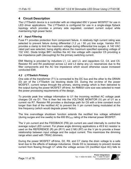
11-Feb-13RDR-347 <strong>12.6</strong> W Dimmable LED Driver Using LYT4313E4 Circuit DescriptionThe LYTSwitch device is a controller with an integrated 650 V power MOSFET <strong>for</strong> use inLED driver applications. The LYTSwitch is configured <strong>for</strong> use in a single-stage flybacktopology which provides a primary side regulated, constant current output whilemaintaining high power factor.4.1 Input FilteringFuse F1 provides protection from component failure. A relatively high current rating wasselected to prevent failure during differential (1.2 s / 50 s) line surge. Varistor RV1provides a clamp to limit the maximum voltage during differential line surges. A 140 VACrated part was selected, being slightly above the maximum specified operating voltage of132 VAC. Diode bridge BR1 rectifies the AC line voltage with capacitor C5 providing alow impedance path (decoupling) <strong>for</strong> the primary switching current.EMI filtering is provided by inductors L1, L2, and L3, and capacitors C2, C4, and C5.Resistor R3 and R4 positioned across L2 and L3 damp any LC resonances due to thefilter components and the AC line impedance which would otherwise cause increasedconducted EMI.4.2 LYTSwitch PrimaryOne side of the trans<strong>for</strong>mer (T1) is connected to the DC bus and the other to the DRAIN(D) pin of the LYTSwitch via blocking diode D3. During the on-time of the powerMOSFET, current ramps through the primary, storing energy which is then delivered tothe output during the power MOSFET off-time. An RM6S/I core size was selected to meetthe power processing requirements of the design.To provide peak line voltage in<strong>for</strong>mation to U1 the incoming rectified AC voltage peakcharges C6 via D1. This is then fed into the VOLTAGE MONITOR (V) pin of U1 as acurrent via R7. Resistor R6 provides a discharge path <strong>for</strong> C6 with a time constant muchlonger than that of the rectified AC to prevent the V pin current being modulated at theline frequency (which would degrade power factor).The line overvoltage shutdown function extends the rectified line voltage withstand(during surges and line swells) to the 650 BV DSS rating of the internal power MOSFET.The V pin current and the FEEDBACK (FB) pin current are used internally to control theaverage output LED current. For phase angle dimming applications a 49.9 k resistor isused on the REFERENCE (R) pin (R11) and 2 M (R7) on the V pin to provide a linearrelationship between input voltage and the output current. This maximizes the dimmingrange when used with <strong>TRIAC</strong> dimmers.During the power MOSFET off-time, D2, R9, and C7 clamp the drain voltage to a safelevel due to the effects of leakage inductance. Diode D3 is necessary to prevent reversecurrent from flowing through U1 while the voltage across C5 (rectified input AC) falls toPage 11 of 78Power IntegrationsTel: +1 408 414 9200 Fax: +1 408 414 9201www.powerint.com


