14-Stage Binary Ripple Counter with Oscillator MC54 ... - Datasheets
14-Stage Binary Ripple Counter with Oscillator MC54 ... - Datasheets
14-Stage Binary Ripple Counter with Oscillator MC54 ... - Datasheets
- No tags were found...

You also want an ePaper? Increase the reach of your titles
YUMPU automatically turns print PDFs into web optimized ePapers that Google loves.
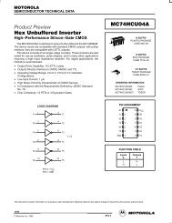
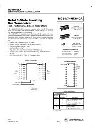
SEMICONDUCTOR TECHNICAL DATA High–Performance Silicon–Gate CMOSThe <strong>MC54</strong>/74HC4060 is identical in pinout to the standard CMOSMC<strong>14</strong>060B. The device inputs are compatible <strong>with</strong> standard CMOS outputs;<strong>with</strong> pullup resistors, they are compatible <strong>with</strong> LSTTL outputs.This device consists of <strong>14</strong> master–slave flip–flops and an oscillator <strong>with</strong> afrequency that is controlled either by a crystal or by an RC circuit connectedexternally. The output of each flip–flop feeds the next, and the frequency ateach output is half that of the preceding one. The state of the counteradvances on the negative–going edge of Osc In. The active–high Reset isasynchronous and disables the oscillator to allow very low power consumptionduring standby operation.State changes of the Q outputs do not occur simultaneously because ofinternal ripple delays. Therefore, decoded output signals are subject todecoding spikes and may need to be gated <strong>with</strong> Osc Out 2 of the HC4060.• Output Drive Capability: 10 LSTTL Loads• Outputs Directly Interface to CMOS, NMOS, and TTL• Operating Voltage Range: 2 to 6 V• Low Input Current: 1 µA• High Noise Immunity Characteristic of CMOS Devices• In Compliance <strong>with</strong> the Requirements Defined by JEDEC StandardNo. 7A• Chip Complexity: 390 FETs or 97.5 Equivalent Gates161616111J SUFFIXCERAMIC PACKAGECASE 620–10PIN ASSIGNMENTN SUFFIXPLASTIC PACKAGECASE 648–08ORDERING INFORMATION<strong>MC54</strong>HCXXXXJMC74HCXXXXNMC74HCXXXXDTDT SUFFIXTSSOP PACKAGECASE 948F–01CeramicPlasticTSSOPOSC INRESET 12LOGIC DIAGRAMOSC OUT 1 OSC OUT 210 911PIN 16 = VCCPIN 8 = GND7546<strong>14</strong>1315123Q4Q5Q6Q7Q8Q9Q10Q12Q13Q<strong>14</strong>Q12Q13121615VCCQ10Q<strong>14</strong> 3 <strong>14</strong> Q8Q6 4 13 Q9Q5 5 12 RESETQ7 6 11 OSC INQ4 7 10 OSC OUT 1GND 89 OSC OUT 2FUNCTION TABLEClock Reset Output StateLNo ChangeL Advance to Next StateX H All Outputs are Low10/95© Motorola, Inc. 19951 REV 6
<strong>MC54</strong>/74HC4060TIMING REQUIREMENTS (Input tr = tf = 6 ns)ÎÎÎÎÎÎÎÎÎÎÎÎÎÎÎÎÎÎÎÎÎÎÎÎÎÎÎÎÎÎÎÎÎÎÎÎÎÎÎÎÎÎÎÎÎÎÎÎÎÎÎÎÎÎÎÎÎÎÎÎÎÎÎÎÎÎÎÎÎÎÎÎÎÎÎÎÎÎÎÎÎÎÎÎÎÎÎÎÎÎÎÎÎÎÎÎÎÎÎÎÎÎÎÎÎÎÎÎSymboltrecParameterMinimum Recovery Time, Reset Inactive to Osc In*(Figure 2)VCCV– 55 to25 CGuaranteed Limit 85 C 125 CÎÎÎÎÎÎÎÎÎÎÎÎÎÎÎÎÎÎÎÎÎÎÎÎÎÎÎÎÎÎÎÎÎÎÎÎÎÎÎÎÎÎÎÎÎÎÎÎÎÎÎÎÎÎÎÎÎÎÎÎÎÎÎÎÎÎÎÎÎÎÎÎÎÎÎÎÎÎÎÎÎÎÎÎÎÎÎÎÎÎÎÎÎÎÎÎÎÎÎÎÎÎÎÎtwtwMinimum Pulse Width, Osc In(Figure 1)Minimum Pulse Width, Reset(Figure 2)ÎÎÎÎÎÎÎÎÎÎÎÎÎÎÎÎÎÎÎÎÎÎÎÎÎÎÎÎÎÎÎ ÎÎÎÎÎÎÎÎÎÎÎÎÎÎÎÎÎÎÎÎÎÎÎÎÎÎÎÎÎÎÎÎÎÎÎÎÎÎÎÎÎÎÎÎÎÎÎÎÎÎÎÎÎÎÎÎÎÎÎÎÎÎÎÎÎÎÎÎÎÎÎÎÎÎÎtr, tfMaximum Input Rise and Fall Times(Figure 1)ÎÎÎÎÎÎÎÎÎÎÎÎÎÎ ÎÎÎÎÎÎÎÎÎÎÎÎÎÎÎÎÎÎÎÎÎÎÎÎÎÎÎÎÎÎÎÎÎÎÎÎÎÎÎÎÎÎÎÎÎÎÎÎÎÎÎÎÎÎÎÎ ÎÎÎÎÎÎÎÎÎ ÎÎÎÎ ÎÎÎÎ ÎÎÎ ÎÎÎÎÎÎÎÎÎÎÎÎÎÎÎÎÎÎÎÎÎÎÎÎÎNOTE: Information on typical parametric values can be found in Chapter 2 of the Motorola High–Speed CMOS Data Book (DL129/D).* Osc In driven <strong>with</strong> external clock.PIN DESCRIPTIONSÎÎÎÎÎÎÎÎÎÎÎÎÎÎÎÎÎÎÎÎÎÎÎÎÎÎÎÎÎÎÎÎÎÎ2.04.56.02.04.56.02.04.56.02.04.56.010020178016<strong>14</strong>8016<strong>14</strong>100050040012525211002017100201710005004001503026120242012024201000500400UnitnsnsnsnsÎÎÎÎÎÎÎÎÎÎÎÎÎÎÎÎÎÎÎÎÎÎÎÎÎÎÎÎÎÎÎÎÎÎINPUTSOsc In (Pin 11)Negative–edge triggering clock input. A high–to–low transitionon this input advances the state of the counter. Osc Inmay be driven by an external clock source.Reset (Pin 12)Active–high reset. A high level applied to this input asynchronouslyresets the counter to its zero state (forcing all Q outputslow) and disables the oscillator.OSC INQ190%50%10%tftr90%VCC50%10%GNDtwtPLH1/fmaxtTLHtPHLFigure 1.tTHLOUTPUTSSWITCHING WAVEFORMSQ4–Q10, Q12–Q<strong>14</strong> (Pins 7, 5, 4, 6, <strong>14</strong>, 13, 15, 1, 2, 3)Active–high outputs. Each QN output divides the oscillatorfrequency by 2N. The user should note that Q1, Q2, Q3, andQ11 are not available as outputs.Osc Out 1, Osc Out 2 (Pins 10, 9)<strong>Oscillator</strong> outputs. These pins are used in conjunction <strong>with</strong>Osc In and the external components to form an oscillator.(See Figures 4 and 5). When Osc In is being driven <strong>with</strong> anexternal clock source, Osc Out 1 and Osc Out 2 must be leftopen circuited. With the crystal oscillator configuration in Figure6, Osc Out 2 must be left open circuited.RESETQCLOCKtPHL50%tw50%trecFigure 2.50%TEST POINTVCCGNDVCCGNDQN50%VCCGNDDEVICEUNDERTESTOUTPUTCL*tPLHtPHLQN + 150%* Includes all probe and jig capacitanceFigure 3.Figure 4. Test CircuitMOTOROLA4High–Speed CMOS Logic DataDL129 — Rev 6
<strong>MC54</strong>/74HC4060EXPANDED LOGIC DIAGRAMQ47Q55Q121Q132Q<strong>14</strong>3CQCQCQCQCQCQCQCQCQCQCQCRRRRRROSC OUT 2OSC OUT 1910Q6 = PIN 4Q7 = PIN 6Q8 = PIN <strong>14</strong>Q9 = PIN 13Q10 = PIN 15VCC = PIN 16GND = PIN 8OSC IN11RESET12For 2.0 V ≤ VCC ≤ 6.0 V10 Rtc > RS > 2 Rtc400 Hz ≤ f ≤ 400 kHzRESET 12 OSC IN 11 OSC OUT 1 10 OSC OUT 2 91f ≈3 RtcCtc(f in Hz, Rtc in ohms, Ctc in farads)RSRtcCtcThe formula may vary for other frequencies.Figure 5. <strong>Oscillator</strong> Circuit Using RC ConfigurationHigh–Speed CMOS Logic DataDL129 — Rev 65 MOTOROLA
<strong>MC54</strong>/74HC4060RESET 12 11 OSC IN 10 OSC OUT 1 9 OSC OUT 2RfR1C1C2Figure 6. Pierce Crystal <strong>Oscillator</strong> CircuitTable 1. Crystal <strong>Oscillator</strong> Amplifier SpecificationsTA = 25 C (Input = Pin 11, Output = Pin 10)TypeInput Resistance, RinOutput Impedance, Zout (4.5 V supply)Input Capacitance, CinOutput Capacitance, CoutSeries Capacitance, Ca3 Vdc supplyÎÎÎÎÎÎÎÎÎÎÎÎÎÎÎÎÎÎÎÎÎÎÎÎÎÎÎÎÎÎÎÎÎÎÎÎÎÎÎÎÎÎÎÎÎÎÎÎÎÎÎÎÎÎÎÎÎÎÎÎÎÎÎÎÎÎÎÎÎÎÎÎÎÎÎÎÎÎÎÎÎÎÎÎÎÎÎÎÎÎÎÎÎÎÎÎÎÎÎÎÎÎÎÎÎÎÎÎÎÎÎÎÎÎÎÎÎÎÎÎÎÎÎÎÎÎÎÎÎÎÎÎÎÎÎÎÎOpen loop voltage4 Vdc supplygain <strong>with</strong> output atfull swing, α5 Vdc supply6 Vdc supplyPositive Reactance (Pierce)60 MΩ minimum200 Ω (see text)5 pF typical7 pF typical5 pF typical5.0 expected minimum4.0 expected minimum3.3 expected minimum3.1 expected minimumÎÎÎÎÎÎÎÎÎÎÎÎÎÎÎÎÎÎÎÎPIERCE CRYSTAL OSCILLATOR DESIGNÎÎÎÎÎÎÎÎÎÎÎÎÎÎÎÎÎÎÎÎÎÎÎÎÎÎÎÎÎÎÎÎÎÎÎÎÎÎÎÎRS LSCS1 2121 Re Xe 2COValues are supplied by crystal manufacturer (parallel resonant crystal)Figure 7. Equivalent Crystal NetworksRs–jXC2RRloadCajXLs–jXCsZload–jXCo–jXCXloadCinCoutNOTE: C = C1 + Cin and R = R1 + Rout. Co is considered as part of theload. Ca and Rf typically have minimal effect below 2 MHz.Figure 8. Series Equivalent Crystal LoadValues are listed in Table 1.Figure 9. Parasitic Capacitancesof the AmplifierMOTOROLA6High–Speed CMOS Logic DataDL129 — Rev 6
<strong>MC54</strong>/74HC4060DESIGN PROCEDURESThe following procedure applies for oscillators operating below 2 MHz where Z is a resistor R1. Above 2 MHz, additional impedanceelements should be considered: Cout and Ca of the amp, feedback resistor Rf, and amplifier phase shift error from 180 .Step 1: Calculate the equivalent series circuit of the crystal at the frequency of oscillation.– jXCo(Rs + jXLs– jXCsZe == Re + jXe– jXCo+ Rs + jXLs– jXCsReactance jXe should be positive, indicating that the crystal is operating as an inductive reactance at the oscillation frequencyThe maximum Rs for the crystal should be used in the equation.Step 2: Determine β, the attenuation, of the feedback network. For a closed–loop gain of 2, Aνβ = 2,β = 2/Aν where Aν isthe gain of the HC4060 amplifier.Step 3: Determine the manufacturer’s loading capacitance. For example: A manufacturer may specify an external load capacitanceof 32 pF at the required frequency.Step 4: Determine the required Q of the system, and calculate Rload. For example, a manufacturer specifies a crystal Qof 100,000. In–circuit Q is arbitrarily set at 20% below crystal Q or 80,000. Then Rload = (2πfoLs/Q) – Rs where Ls and Rs arecrystal parameters.Step 5: Simultaneously solve, using a computer,XC • XC2β =R • R e + XC2 (Xe – XC)(<strong>with</strong> feedback phase shift = 180 )(1)Xe = XC2 + XC +ReXC2R= XCload(where the loading capacitor is an external load, not including Co)(2)Rload =RXCo X C2[(XC + XC2) (XC + XCo ) – XC(XC + XCo+ XC2)]X2 C2 (XC + XCo)2+ R2(XC + XCo + X C2)2(3)Here R = Rout + R1. Rout is amp output resistance, R1 is Z. The C corresponding to XC is given by C = C1 + Cin.Alternately, pick a value for R1 (i.e., let R1 = Rs). Solve Equations 1 and 2 for C1 and C2. Use Equation 3 and the fact thatQ = 2πfoLs/(Rs + Rload) to find in–circuit Q. If Q is not satisfactory pick another value for R1 and repeat the procedure.CHOOSING R1Power is dissipated in the effective series resistance of thecrystal. The drive level specified by the crystal manufactureris the maximum stress that a crystal can <strong>with</strong>stand <strong>with</strong>outdamage or excessive shift in frequency R1 limits the drivelevel.To verify that the maximum dc supply voltage does notoverdrive the crystal, monitor the output frequency as a functionof voltage at Osc Out 2 (Pin 9). The frequency shouldincrease very slightly as the dc supply voltage is increased.An overdriven crystal will decrease in frequency or becomeunstable <strong>with</strong> an increase in supply voltage. The operatingsupply voltage must be reduced or R1 must be increased invalue it the overdriven condition exists. The user should notethat the oscillator start–up time is proportional to the value ofR1.SELECTING RfThe feedback resistor, Rf, typically ranges up to 20 MΩ. Rfdetermines the gain and bandwidth of the amplifier. Properbandwidth insures oscillation at the correct frequency plusroll–off to minimize gain at undesirable frequencies, such asthe first overtone. Rf must be large enough so as to not affectthe phase of the feedback network in an appreciable manner.ACKNOWLEDGEMENTS AND RECOMMENDEDREFERENCESThe following publications were used in preparing this datasheet and are hereby acknowledged and recommended forreading:Technical Note TN–24, Statek Corp.Technical Note TN–7, Statek Corp.D. Babin, “Designing Crystal <strong>Oscillator</strong>s”, Machine Design,March 7, 1985.D. Babin, “Guidelines for Crystal <strong>Oscillator</strong> Design”,Machine Design, April 25, 1985.ALSO RECOMMENDED FOR READING:E. Hafner, “The Piezoelectric Crystal Unit – Definitions andMethod of Measurement”, Proc. IEEE, Vol. 57, No. 2, Feb.1969.D. Kemper, L. Rosine, “Quartz Crystals for FrequencyControl”, Electro–Technology, June, 1969.P. J. Ottowitz, “A Guide to Crystal Selection”, ElectronicDesign, May, 1966.High–Speed CMOS Logic DataDL129 — Rev 67 MOTOROLA
<strong>MC54</strong>/74HC4060TIMING DIAGRAMOSC INRESETQ4Q5Q6Q7Q8Q9Q10Q11Q12Q13Q<strong>14</strong>1 2 4 8 16 32 64 128 256 512 1024 20484096 8192 16,384MOTOROLA8High–Speed CMOS Logic DataDL129 — Rev 6
<strong>MC54</strong>/74HC4060OUTLINE DIMENSIONSJ SUFFIXCERAMIC PACKAGECASE 620–10ISSUE V169–A–1 8–B–CLNOTES:1. DIMENSIONING AND TOLERANCING PERANSI Y<strong>14</strong>.5M, 1982.2. CONTROLLING DIMENSION: INCH.3. DIMENSION L TO CENTER OF LEAD WHENFORMED PARALLEL.4. DIM F MAY NARROW TO 0.76 (0.030) WHERETHE LEAD ENTERS THE CERAMIC BODY.–TSEATING –PLANEFEGND 16 PL0.25 (0.010) M T ASKMJ 16 PL0.25 (0.010) M T BSDIMABCDEFGJKLMNINCHESMIN MAX0.750 0.7850.240 0.295— 0.2000.015 0.0200.050 BSC0.055 0.0650.100 BSC0.008 0.0150.125 0.1700.300 BSC0° 15°0.020 0.040MILLIMETERSMIN MAX19.05 19.936.10 7.49— 5.080.39 0.501.27 BSC1.40 1.652.54 BSC0.21 0.383.18 4.317.62 BSC0°0.5115°1.01N SUFFIXPLASTIC PACKAGECASE 648–08ISSUE R16–A–9B1 8NOTES:1. DIMENSIONING AND TOLERANCING PER ANSIY<strong>14</strong>.5M, 1982.2. CONTROLLING DIMENSION: INCH.3. DIMENSION L TO CENTER OF LEADS WHENFORMED PARALLEL.4. DIMENSION B DOES NOT INCLUDE MOLD FLASH.5. ROUNDED CORNERS OPTIONAL.HGFSCK–T–SEATINGPLANED 16 PL0.25 (0.010) M T A MJLMDIMABCDFGHJKLMSINCHESMIN MAX0.740 0.7700.250 0.2700.<strong>14</strong>5 0.1750.015 0.0210.040 0.0700.0080.1100.2950°0.0200.100 BSC0.050 BSC0.0150.1300.30510°0.040MILLIMETERSMIN MAX18.80 19.556.35 6.853.69 4.440.39 0.531.02 1.772.54 BSC1.27 BSC0.212.807.500°0.510.383.307.7410°1.01High–Speed CMOS Logic DataDL129 — Rev 69 MOTOROLA
<strong>MC54</strong>/74HC4060OUTLINE DIMENSIONSDT SUFFIXPLASTIC TSSOP PACKAGECASE 948F–01ISSUE O0.15 (0.006) T0.15 (0.006) T0.10 (0.004)–T– SEATINGPLANELUPIN 1IDENT.UDSS2X L/2C16X K REF0.10 (0.004) M T U S V S16 91 8A–V–GB–U–HNNJJ1FDETAIL EDETAIL EKK1ÇÇ ÉÉÉÉ ÇÇÉÉ ÇÇSECTION N–NÉÉ ÇÇ0.25 (0.010)M–W–NOTES:1. DIMENSIONING AND TOLERANCING PER ANSIY<strong>14</strong>.5M, 1982.2. CONTROLLING DIMENSION: MILLIMETER.3. DIMENSION A DOES NOT INCLUDE MOLD FLASH.PROTRUSIONS OR GATE BURRS. MOLD FLASH ORGATE BURRS SHALL NOT EXCEED 0.15 (0.006) PERSIDE.4. DIMENSION B DOES NOT INCLUDE INTERLEADFLASH OR PROTRUSION. INTERLEAD FLASH ORPROTRUSION SHALL NOT EXCEED0.25 (0.010) PER SIDE.5. DIMENSION K DOES NOT INCLUDE DAMBARPROTRUSION. ALLOWABLE DAMBAR PROTRUSIONSHALL BE 0.08 (0.003) TOTAL IN EXCESS OF THE KDIMENSION AT MAXIMUM MATERIAL CONDITION.6. TERMINAL NUMBERS ARE SHOWN FORREFERENCE ONLY.7. DIMENSION A AND B ARE TO BE DETERMINED ATDATUM PLANE –W–.MILLIMETERS INCHESDIM MIN MAX MIN MAXA 4.90 5.10 0.193 0.200B 4.30 4.50 0.169 0.177C ––– 1.20 ––– 0.047D 0.05 0.15 0.002 0.006F 0.50 0.75 0.020 0.030G 0.65 BSC 0.026 BSCH 0.18 0.28 0.007 0.011J 0.09 0.20 0.004 0.008J1 0.09 0.16 0.004 0.006K 0.19 0.30 0.007 0.012K1 0.19 0.25 0.007 0.010L 6.40 BSC 0.252 BSCM 0 8 0 8Motorola reserves the right to make changes <strong>with</strong>out further notice to any products herein. Motorola makes no warranty, representation or guarantee regardingthe suitability of its products for any particular purpose, nor does Motorola assume any liability arising out of the application or use of any product or circuit,and specifically disclaims any and all liability, including <strong>with</strong>out limitation consequential or incidental damages. “Typical” parameters can and do vary in differentapplications. All operating parameters, including “Typicals” must be validated for each customer application by customer’s technical experts. Motorola doesnot convey any license under its patent rights nor the rights of others. Motorola products are not designed, intended, or authorized for use as components insystems intended for surgical implant into the body, or other applications intended to support or sustain life, or for any other application in which the failure ofthe Motorola product could create a situation where personal injury or death may occur. Should Buyer purchase or use Motorola products for any suchunintended or unauthorized application, Buyer shall indemnify and hold Motorola and its officers, employees, subsidiaries, affiliates, and distributors harmlessagainst all claims, costs, damages, and expenses, and reasonable attorney fees arising out of, directly or indirectly, any claim of personal injury or deathassociated <strong>with</strong> such unintended or unauthorized use, even if such claim alleges that Motorola was negligent regarding the design or manufacture of the part.Motorola and are registered trademarks of Motorola, Inc. Motorola, Inc. is an Equal Opportunity/Affirmative Action Employer.How to reach us:USA/EUROPE: Motorola Literature Distribution;JAPAN: Nippon Motorola Ltd.; Tatsumi–SPD–JLDC, Toshikatsu Otsuki,P.O. Box 20912; Phoenix, Arizona 85036. 1–800–441–2447 6F Seibu–Butsuryu–Center, 3–<strong>14</strong>–2 Tatsumi Koto–Ku, Tokyo 135, Japan. 03–3521–8315MFAX: RMFAX0@email.sps.mot.com –TOUCHTONE (602) 244–6609 HONG KONG: Motorola Semiconductors H.K. Ltd.; 8B Tai Ping Industrial Park,INTERNET: http://Design–NET.com 51 Ting Kok Road, Tai Po, N.T., Hong Kong. 852–26629298MOTOROLA◊CODELINE10<strong>MC54</strong>/74HC4060/DHigh–Speed CMOS Logic DataDL129 — Rev 6