IGBT Driver Calculation - Server application notes
IGBT Driver Calculation - Server application notes
IGBT Driver Calculation - Server application notes

You also want an ePaper? Increase the reach of your titles
YUMPU automatically turns print PDFs into web optimized ePapers that Google loves.
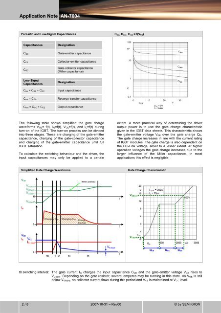
Application Note AN-7004Parasitic and Low-Signal CapacitancesC ies, C oes, C res = f(V CE)CapacitancesDesignationC GEGate-emitter capacitanceC CEC GCCollector-emitter capacitanceGate-collector capacitance(Miller capacitance)Low-SignalCapacitancesC ies = C GE + C GCC res = C GCC oes = C GC + C CEDesignationInput capacitanceReverse transfer capacitanceOutput capacitanceVGE = 0Vf = 1MHzThe following table shows simplified the gate chargewaveforms V GE= f(t), I G=f(t), V CE=f(t), and I C=f(t) duringturn-on of the <strong>IGBT</strong>. The turn-on process can be dividedinto three stages. These are charging of the gate-emittercapacitance, charging of the gate-collector capacitanceand charging of the gate-emitter capacitance until full<strong>IGBT</strong> saturation.To calculate the switching behaviour and the driver, theinput capacitances may only be applied to a certainextent. A more practical way of determining the driveroutput power is to use the gate charge characteristicgiven in the <strong>IGBT</strong> data sheets. This characteristic showsthe gate-emitter voltage V GE over the gate charge Q G.The gate charge increases in line with the current ratingof <strong>IGBT</strong> modules. The gate charge is also dependent onthe DC-Link voltage, albeit to a lesser extent. At higheroperation voltages the gate charge increases due to thelarger influence of the Miller capacitance. In most<strong>application</strong>s this effect is negligible.Simplified Gate Charge WaveformsGate Charge CharacteristicV GE(on)V GE(off)Q GE Q GC Q GEt0 switching interval: The gate current I G charges the input capacitance C GE and the gate-emitter voltage V GE rises toV GE(th). Depending on the gate resistor, several amperes may be running in this state. As V GE is stillbelow V GE(th), no collector current flows during this period and V CE is maintained at V CC level.2 / 8 2007-10-31 – Rev00 © by SEMIKRON