IGBT Driver Calculation - Server application notes
IGBT Driver Calculation - Server application notes
IGBT Driver Calculation - Server application notes

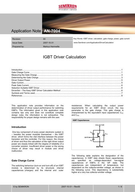
Create successful ePaper yourself
Turn your PDF publications into a flip-book with our unique Google optimized e-Paper software.
Application NoteAN-7004Revision:Issue Date:Prepared by:002007-10-31Markus HermwilleKey Words: <strong>IGBT</strong> driver, calculation, gate charge, power, gate currentwww.Semikron.com/Application/<strong>Driver</strong><strong>Calculation</strong><strong>IGBT</strong> <strong>Driver</strong> <strong>Calculation</strong>Introduction.............................................................................................................................................................................1Gate Charge Curve ................................................................................................................................................................1Measuring the Gate Charge ...................................................................................................................................................3Determining the Gate Charge.................................................................................................................................................3<strong>Driver</strong> Output Power...............................................................................................................................................................5Gate Current...........................................................................................................................................................................5Peak Gate Current..................................................................................................................................................................6Selection Suitable <strong>IGBT</strong> <strong>Driver</strong>...............................................................................................................................................6<strong>Driver</strong>Sel – The Easy <strong>IGBT</strong> <strong>Driver</strong> <strong>Calculation</strong> Method ..........................................................................................................6Symbols and Terms used.......................................................................................................................................................7References .............................................................................................................................................................................8This <strong>application</strong> note provides information on thedetermination of driver output performance for switching<strong>IGBT</strong>s. The information given in this <strong>application</strong> notecontains tips only and does not constitute completedesign rules; the information is not exhaustive. Theresponsibility for proper design remains with the user.resistances. When calculating the output powerrequirements for an <strong>IGBT</strong> driver circuit, the keyparameter is the gate charge. This gate charge ischaracterised by the equivalent input capacitances C GCand C GE.<strong>IGBT</strong> CapacitancesIntroductionOne key component of every power electronic system is– besides the power modules themselves – the <strong>IGBT</strong>driver, which forms the vital interface between the powertransistor and the controller. For this reason, the choiceof driver and thus the calculation of the right driver outputpower are closely linked with the degree of reliability of aconverter solution. Insufficient driver power or the wrongchoice of driver may result in module and drivermalfunction.Gate Charge CurveThe switching behaviour (turn-on and turn-off) of an <strong>IGBT</strong>module is determined by its structural, internalcapacitances (charges) and the internal and outerThe following table explains the designation of thecapacitances. In <strong>IGBT</strong> data sheets these capacitancesare specified as voltage-dependent low-signalcapacitances of <strong>IGBT</strong>s in the “off” state. Thecapacitances are independent of temperature, butdependent on the collector-emitter voltage, as shown inthe following curve. This dependency is substantiallyhigher at a very low collector-emitter voltage.© by SEMIKRON2007-10-31 – Rev001 / 8
Application Note AN-7004Parasitic and Low-Signal CapacitancesC ies, C oes, C res = f(V CE)CapacitancesDesignationC GEGate-emitter capacitanceC CEC GCCollector-emitter capacitanceGate-collector capacitance(Miller capacitance)Low-SignalCapacitancesC ies = C GE + C GCC res = C GCC oes = C GC + C CEDesignationInput capacitanceReverse transfer capacitanceOutput capacitanceVGE = 0Vf = 1MHzThe following table shows simplified the gate chargewaveforms V GE= f(t), I G=f(t), V CE=f(t), and I C=f(t) duringturn-on of the <strong>IGBT</strong>. The turn-on process can be dividedinto three stages. These are charging of the gate-emittercapacitance, charging of the gate-collector capacitanceand charging of the gate-emitter capacitance until full<strong>IGBT</strong> saturation.To calculate the switching behaviour and the driver, theinput capacitances may only be applied to a certainextent. A more practical way of determining the driveroutput power is to use the gate charge characteristicgiven in the <strong>IGBT</strong> data sheets. This characteristic showsthe gate-emitter voltage V GE over the gate charge Q G.The gate charge increases in line with the current ratingof <strong>IGBT</strong> modules. The gate charge is also dependent onthe DC-Link voltage, albeit to a lesser extent. At higheroperation voltages the gate charge increases due to thelarger influence of the Miller capacitance. In most<strong>application</strong>s this effect is negligible.Simplified Gate Charge WaveformsGate Charge CharacteristicV GE(on)V GE(off)Q GE Q GC Q GEt0 switching interval: The gate current I G charges the input capacitance C GE and the gate-emitter voltage V GE rises toV GE(th). Depending on the gate resistor, several amperes may be running in this state. As V GE is stillbelow V GE(th), no collector current flows during this period and V CE is maintained at V CC level.2 / 8 2007-10-31 – Rev00 © by SEMIKRON
Application Note AN-7004t1 switching interval: As soon as V GE passes V GE(th), the <strong>IGBT</strong> turn-on process starts. I C begins to increase to reach the fullload current I C(load), which is valid for an ideal free-wheeling diode (shown in the simplified waveform).For a real free-wheeling diode, I C exceeds I C(load). This is because a reverse recovery current, whichflows in reverse direction, is added to I C(load). Since the free-wheeling diode is still conducting currentat the beginning of section t2, the collector-emitter voltage V CE will not drop. V GE reaches the plateauvoltage V GE(pl).t2 switching interval: V GE maintains V GE(pl). When the free-wheeling diode is turned-off, V CE starts to drop rapidly anddv CE/dt is high.t3 switching interval: While V CE is decreasing to reach on-state value V CEsat, the Miller capacitance C GC increases as thevoltage decreases and is charged by I G. V GE still remains on a plateau, which is V GE(pl) level.t4 switching interval: At the beginning of section t4, the <strong>IGBT</strong> is fully turned-on. The charge conducted to C GE induces anexponential increase in V GE up to the gate control voltage V GE(on). I G ends with an exponential fade outand V CE reaches V CEsat level.During turn-off the processes described are running in reverse direction. The charge has to be removed from the gate.Measuring the Gate ChargeA simplified test circuit that can be used to measure thegate charge is shown in the following table. The gate issupplied by a constant gate current. Furthermore, a pulseconstant collector current is applied. The constant gatecurrent causes the measured waveform V GE = f(t) to beequivalent to V GE = f(Q G) due to Q G = I G × t.The document IEC 60747-9, Ed.2: SemiconductorDevices – Discrete Devices – Part 9: Insulated-GateBipolar Transistors (<strong>IGBT</strong>s) describes the gate chargetest method.Basis Test Circuit for Gate Charge Measurement Waveform V GE = f(t) ⇔ V GE = f(Q G)Determining the Gate ChargeThe gate charge per pulse needed to drive the <strong>IGBT</strong> canbe determined using the gate charge characteristicdiagram, which shows gate-emitter voltage over gatecharge. The total gate charge can be read out by takinginto account the amplitude of the applied gate voltage,i.e. from turn-on gate voltage V G(on) to turn-off gatevoltage V G(off). The SEMIKRON <strong>IGBT</strong> data sheet showsthe gate charge curve in the positive and negativequadrant.If the gate charge curve is given in the positive quadrantonly, the gate charge amplitude can be read out byextrapolation, as shown in the following table. The brightgreen represents the area of a diagram given in the <strong>IGBT</strong>data sheet. A parallel adjustment of the bright green areaalong the gate charge curve into the negative quadrantup to V G(off) allows for the amplitude of the gate charge tobe determined.© by SEMIKRON2007-10-31 – Rev003 / 8
Application Note AN-7004Gate Charge Characteristic (e.g. SKM400GB126D)Extrapolation MethodV G(on)V G(off)Q GAnother method for determining the gate charge uses theinput capacitance C ies and a special factor instead of thegate charge curve. The value for C ies is given in the <strong>IGBT</strong>data sheet.The necessary gate charge or the charging energy perpulse must be available at the right time. This can onlybe achieved by using low-impedance, low-inductanceoutput capacitors at the driver output stage. The size ofthe capacitors is indicated by the calculated value Q G.The gate charge is the basic parameter used todetermine driver output power and gate current.Gate Charge <strong>Calculation</strong> with C ies MethodThe gate charge can be expressed asPlease note:This method is not entirely accurate and should be onlyused if no gate charge curve is available.QG= CG× (VG(on)− VG(off))where C = k × CGCiesThe gate capacitance factor k c can be roughly calculated askC=CiesQ× (VG(ds)G(on)− VG(off )where Q G(ds) is the value specified in the <strong>IGBT</strong> data sheet, andV G(on) as well as V G(off) are the gate voltages applied to Q G(ds).Thus, the alternative gate charge calculation is as follows:QG= kC× Cies× (VG(on)− VG(off)))4 / 8 2007-10-31 – Rev00 © by SEMIKRON
Application Note AN-7004<strong>Driver</strong> Output PowerThe individual power of each internal supply needed todrive the <strong>IGBT</strong> can be found as a function of the intendedswitching frequency and the energy which has to be usedto charge and discharge the <strong>IGBT</strong>.<strong>Calculation</strong> of <strong>Driver</strong> Output Power per ChannelPower can be expressed asP = E × fGD(out )Substituting = Q × (V − V ),swEG G(on) G(off )Rough calculation of driver power using the C ies method:2PGD(out)= kC× Cies× (VG(on)− VG(off)) ×fswthe driver output power per channel is:P = Q × (V − V ) × fGD(out)GG(on)G(off )swGate CurrentOne of the key requirements for <strong>IGBT</strong> driver circuits isthat enough current be supplied to charge and dischargethe input capacitances of the <strong>IGBT</strong> and thus to switch the<strong>IGBT</strong> on and off. This gate current can be calculatedusing the equations for <strong>IGBT</strong> input capacitance charging.The gate current calculated is the minimum averageoutput current I outAVG of the driver output stage perchannel.<strong>IGBT</strong> Capacitances<strong>Calculation</strong> of Gate CurrentCharge can be calculated as follows:Q G= ∫ idtWithQ ×GE= iGEt ,swQGC= iGC× tswthe total gate charge is:Q = Q + Q = (i + i ) × tGGEGCGEGCswSubstitutingt =1f swthe average gate current is:I = I + I = Q × fGGEGCGswRoughly calculation of average gate current by using the C ies method::I = k × C × (V − V ) × fGCiesG(on)G(off )sw© by SEMIKRON2007-10-31 – Rev005 / 8
Application Note AN-7004Peak Gate CurrentThe <strong>IGBT</strong> switching time is controlled by charging anddischarging the gate of the <strong>IGBT</strong>. If the gate peak currentis increased, the turn-on and turn-off time will be shorterand the switching losses reduced. This obviously has animpact on other switching parameters such asovervoltage stress, which have to be watched. The gatecharge currents can be controlled by the gate resistorsR G(on) and R G(off). The theoretical peak current valueI GPEAK can be calculated using the equation below. The<strong>IGBT</strong> module's internal gate resistor R G(int) must be takeninto account when calculating the peak gate current. Inpractice, stray inductance reduces the peak value belowthe possible theoretical value.Peak Gate Current<strong>Calculation</strong>The peak gate current can be calculated as follows:IGPEAKV=RG(on)G− V+ RG(off )G(int)In the data sheet of an <strong>IGBT</strong> driver, a maximum peakcurrent is given, as are the minimum values for the gateresistors. If both these maximum and minimum ratingsare exceeded, the driver output may be destroyed as aresult.Selection Suitable <strong>IGBT</strong> <strong>Driver</strong>When selecting the suitable <strong>IGBT</strong> driver for the individual<strong>application</strong>, the following details have to be considered: The driver must be able to provide the necessary gatecurrent (output current / output power). The maximumaverage output current of the driver must be higherthan the calculated value. The maximum peak gate current of the driver must beequal to or higher than maximum calculated peak gatecurrent. The output capacitors of the driver must be able todeliver the gate charge needed to charge anddischarge the gate of the <strong>IGBT</strong>. In the data sheet ofSEMIKRON drivers the maximum charge per pulse isgiven. This value must be duly considered whenselecting a suitable driver.Other parameters worth mentioning in the context of<strong>IGBT</strong> driver selection are insulation voltage and dv/dtcapability.<strong>Driver</strong>Sel – The Easy <strong>IGBT</strong> <strong>Driver</strong><strong>Calculation</strong> Method<strong>Driver</strong>Sel facilitates <strong>IGBT</strong> driver calculation and theselection of a suitable driver, regardless of the<strong>application</strong>. This software tool takes into considerationthe aforementioned characteristics and equations, andcalculates suitable <strong>IGBT</strong> drivers on the basis of the <strong>IGBT</strong>module selected, the number of paralleled modules, gateresistor, switching frequency and collector-emittervoltage. This tool can be used for driver calculation andselection for any brand and <strong>IGBT</strong> package, as well as tocalculate the necessary gate charge and averagecurrent.Link: DrivelSel is a free software tool and is available on the SEMIKRON homepage at http://semisel.semikron.com/<strong>Driver</strong>SelectTool.asp.6 / 8 2007-10-31 – Rev00 © by SEMIKRON
Application Note AN-7004<strong>Driver</strong>Sel ScreenshotSymbols and Terms usedLetter SymbolC CEC GC GCC GEC iesC oesC resdv CE/dtEf swI CI CpulsI GI GMI outAVGk CP GD(out)Q GQ GCQ GER GR G(int)TermCollector-emitter capacitanceEffective gate capacitanceGate-collector capacitanceGate-emitter capacitanceInput capacitance <strong>IGBT</strong>Output capacitance <strong>IGBT</strong>Reverse transfer capacitance <strong>IGBT</strong>Rate of rise and fall of collector-emitter voltageElectrical energySwitching frequencyCollector currentPulse constant collector currentGate currentPeak gate currentAverage output current of the driverGate capacitance factor<strong>Driver</strong> output powerGate chargeGate-collector chargeGate-emitter chargeGate resistor<strong>IGBT</strong> module internal gate resistor© by SEMIKRON2007-10-31 – Rev007 / 8
Application Note AN-7004R G(off)R G(on)tt swV CCV CEV CEsatV GV G(off)V G(on)V GEV GE(pl)V GE(th)Turn-off gate resistorTurn-on gate resistorTimeSwitching timeCollector-emitter supply voltageCollector-emitter voltageCollector-emitter saturation voltageGate voltage (output driver)Turn-off gate voltage (output driver)Turn-on gate voltage (output driver)Gate-emitter voltagePlateau gate-emitter during switchingGate-emitter threshold voltageReferences[1] www.SEMIKRON.com[2] Application Manual Power Modules, SEMIKRONInternational[3] M. Hermwille, "Plug and Play <strong>IGBT</strong> <strong>Driver</strong> Cores forConverters", Power Electronics Europe Issue 2, pp.10-12, 2006[4] M. Hermwille, "Gate Resistor – Principle andApplication", Application Note AN-7003, SEMIKRON[5] P. Bhosale, M. Hermwille, "Connection of Gate<strong>Driver</strong>s to <strong>IGBT</strong> and Controller", Application Note AN-7002, SEMIKRON[6] IEC 60747-9, Ed.2: Semiconductor Devices –Discrete Devices – Part 9: Insulated-Gate BipolarTransistors (<strong>IGBT</strong>s)DISCLAIMERSEMIKRON reserves the right to make changes without further notice herein to improve reliability, function or design.Information furnished in this document is believed to be accurate and reliable. However, no representation or warranty isgiven and no liability is assumed with respect to the accuracy or use of such information. SEMIKRON does not assume anyliability arising out of the <strong>application</strong> or use of any product or circuit described herein. Furthermore, this technical informationmay not be considered as an assurance of component characteristics. No warranty or guarantee expressed or implied ismade regarding delivery, performance or suitability. This document supersedes and replaces all information previouslysupplied and may be superseded by updates without further notice.SEMIKRON products are not authorized for use in life support appliances and systems without the express written approvalby SEMIKRON.SEMIKRON INTERNATIONAL GmbHP.O. Box 820251 • 90253 Nürnberg • Deutschland • Tel: +49 911-65 59-234 • Fax: +49 911-65 59-262sales.skd@semikron.com • www.semikron.com11283440 11/20078 / 8 2007-10-31 – Rev00 © by SEMIKRON