1K-16K UNI/O⢠Serial EEPROM Family Data Sheet - Microchip
1K-16K UNI/O⢠Serial EEPROM Family Data Sheet - Microchip
1K-16K UNI/O⢠Serial EEPROM Family Data Sheet - Microchip
- No tags were found...

Create successful ePaper yourself
Turn your PDF publications into a flip-book with our unique Google optimized e-Paper software.
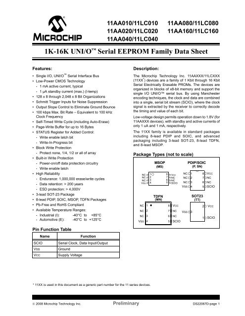
11AA010/11LC010 11AA080/11LC08011AA020/11LC020 11AA160/11LC16011AA040/11LC040<strong>1K</strong>-<strong>16K</strong> <strong>UNI</strong>/O <strong>Serial</strong> <strong>EEPROM</strong> <strong>Family</strong> <strong>Data</strong> <strong>Sheet</strong>Features:• Single I/O, <strong>UNI</strong>/O <strong>Serial</strong> Interface Bus• Low-Power CMOS Technology- 1 mA active current, typical- 1 µA standby current (max.) (I-temp)• 128 x 8 through 2,048 x 8 Bit Organizations• Schmitt Trigger Inputs for Noise Suppression• Output Slope Control to Eliminate Ground Bounce• 100 kbps Max. Bit Rate – Equivalent to 100 kHzClock Frequency• Self-Timed Write Cycle (including Auto-Erase)• Page-Write Buffer for up to 16 Bytes• STATUS Register for Added Control:- Write enable latch bit- Write-In-Progress bit• Block Write Protection- Protect none, 1/4, 1/2 or all of array• Built-in Write Protection- Power-on/off data protection circuitry- Write enable latch• High Reliability- Endurance: 1,000,000 erase/write cycles- <strong>Data</strong> retention: > 200 years- ESD protection: > 4,000V• 3-lead SOT-23 Package• 8-lead PDIP, SOIC, MSOP, TDFN Packages• Pb-Free and RoHS Compliant• Available Temperature Ranges:- Industrial (I): -40°C to +85°C- Automotive (E): -40°C to +125°CDescription:The <strong>Microchip</strong> Technology Inc. 11AAXXX/11LCXXX(11XX * ) devices are a family of 1 Kbit through 16 Kbit<strong>Serial</strong> Electrically Erasable PROMs. The devices areorganized in blocks of x8-bit memory and support thesingle I/O <strong>UNI</strong>/O serial bus. By using Manchesterencoding techniques, the clock and data are combinedinto a single, serial bit stream (SCIO), where the clocksignal is extracted by the receiver to correctly decodethe timing and value of each bit.Low-voltage design permits operation down to 1.8V (for11AAXXX devices), with standby and active currents ofonly 1 uA and 1 mA, respectively.The 11XX family is available in standard packagesincluding 8-lead PDIP and SOIC, and advancedpackaging including 3-lead SOT-23, 8-lead TDFN,and 8-lead MSOP.Package Types (not to scale)NCNCNCVSSNCNCNCVSS1234MSOP(MS)TDFN(MN)8765VCCNCNCSCIONCNCNCVSS1 8 VCC234765NCNCSCIOVSSPDIP/SOIC(P, SN)12348765SOT23(TT)32VCCNCNCSCIOVCC1 SCIOPin Function TableNameFunctionSCIO <strong>Serial</strong> Clock, <strong>Data</strong> Input/OutputVSSGroundVCC Supply Voltage* 11XX is used in this document as a generic part number for the 11 series devices.© 2008 <strong>Microchip</strong> Technology Inc. Preliminary DS22067D-page 1
11AAXXX/11LCXXXDEVICE SELECTION TABLEPart NumberDensity(bits)OrganizationVCC RangePage Size(Bytes)Temp.RangesPackages11LC010 <strong>1K</strong> 128 x 8 2.5-5.5V 16 I,E P, SN, MS, MN, TT11AA010 <strong>1K</strong> 128 x 8 1.8-5.5V 16 I P, SN, MS, MN, TT11LC020 2K 256 x 8 2.5-5.5V 16 I,E P, SN, MS, MN, TT11AA020 2K 256 x 8 1.8-5.5V 16 I P, SN, MS, MN, TT11LC040 4K 512 x 8 2.5-5.5V 16 I,E P, SN, MS, MN, TT11AA040 4K 512 x 8 1.8-5.5V 16 I P, SN, MS, MN, TT11LC080 8K 1,024 x 8 2.5-5.5V 16 I,E P, SN, MS, MN, TT11AA080 8K 1,024 x 8 1.8-5.5V 16 I P, SN, MS, MN, TT11LC160 <strong>16K</strong> 2,048 x 8 2.5-5.5V 16 I,E P, SN, MS, MN, TT11AA160 <strong>16K</strong> 2,048 x 8 1.8-5.5V 16 I P, SN, MS, MN, TTDS22067D-page 2 Preliminary © 2008 <strong>Microchip</strong> Technology Inc.
11AAXXX/11LCXXX1.0 ELECTRICAL CHARACTERISTICSAbsolute Maximum Ratings (†)VCC.............................................................................................................................................................................6.5VSCIO w.r.t. VSS.....................................................................................................................................-0.6V to VCC+1.0VStorage temperature ................................................................................................................................. -65°C to 150°CAmbient temperature under bias............................................................................................................... -40°C to 125°CESD protection on all pins.......................................................................................................................................... 4 kV† NOTICE: Stresses above those listed under ‘Absolute Maximum Ratings’ may cause permanent damage to thedevice. This is a stress rating only and functional operation of the device at those or any other conditions above thoseindicated in the operational listings of this specification is not implied. Exposure to maximum rating conditions for anextended period of time may affect device reliability.TABLE 1-1: DC CHARACTERISTICSElectrical Characteristics:DC CHARACTERISTICSIndustrial (I): VCC = 2.5V to 5.5V TA = -40°C to +85°CVCC = 1.8V to 2.5V TA = -20°C to +85°CAutomotive (E): VCC = 2.5V to 5.5V TA = -40°C to +125°CParam.No.Sym. Characteristic Min. Max. Units Test ConditionsD1 VIH High-level input 0.7*VCC VCC+1 VvoltageD2 VIL Low-level inputvoltageD3 VHYS Hysteresis of SchmittTrigger inputs (SCIO)D4 VOH High-level outputvoltageD5 VOL Low-level outputvoltageD6 IO Output current limit(Note 2)D7 ILI Input leakage current(SCIO)D8 CINT Internal Capacitance(all inputs andoutputs)D9 ICC Read Read OperatingCurrentD10 ICC Write Write OperatingCurrent-0.3-0.30.3*VCC0.2*VCCVVVCC ≥ 2.5VVCC < 2.5V0.05*Vcc — V VCC ≥ 2.5V (Note 1)VCC -0.5VCC -0.5——————0.40.4±4±3VVVVmAmAIOH = -300 μA, VCC = 5.5VIOH = -200 μA, Vcc = 2.5VIOI = 300 μA, VCC = 5.5VIOI = 200 μA, Vcc = 2.5VVCC = 5.5V (Note 1)Vcc = 2.5V (Note 1)— ±1 μA VIN = VSS or VCC— 7 pF TA = 25°C, FCLK = 1 MHz,VCC = 5.0V (Note 1)————D11 Iccs Standby Current —31535mAmAmAmAμAVCC=5.5V; FBUS=100 kHz, CB=100 pFVCC=2.5V; FBUS=100 kHz, CB=100 pFVCC = 5.5VVCC = 2.5VVCC = 5.5VTA = 125°C— 1 μA VCC = 5.5VTA = 85°CD12 ICCI Idle Mode Current — 50 μA VCC = 5.5VNote 1: This parameter is periodically sampled and not 100% tested.2: The SCIO output driver impedance will vary to ensure IO is not exceeded.© 2008 <strong>Microchip</strong> Technology Inc. Preliminary DS22067D-page 3
11AAXXX/11LCXXXTABLE 1-2:AC CHARACTERISTICSElectrical Characteristics:AC CHARACTERISTICSIndustrial (I): VCC = 2.5V to 5.5V TA = -40°C to +85°CVCC = 1.8V to 2.5V TA = -20°C to +85°CAutomotive (E): VCC = 2.5V to 5.5V TA = -40°C to +125°CParam.No.Sym. Characteristic Min. Max. Units Test Conditions1 FBUS <strong>Serial</strong> bus frequency 10 100 kHz —2 TE Bit period 10 100 µs —3 TIJIT Input edge jitter tolerance — ±0.10 UI (Note 3)4 FDRIFT <strong>Serial</strong> bus frequency driftrate tolerance— ±0.75 % per byte —5 FDEV <strong>Serial</strong> bus frequency driftlimitTABLE 1-3:AC TEST CONDITIONS— ±6 % percommand6 TOJIT Output edge jitter — ±0.25 UI (Note 3)7 TR SCIO input rise time— 100 ns —(Note 1)8 TF SCIO input fall time— 100 ns —(Note 1)9 TSTBY Standby pulse time 600 — µs —10 TSS Start header setup time 10 — µs —11 THDR Start header low pulse 5 — µs —time12 TSP Input filter spikesuppression (SCIO)— 50 ns (Note 1)13 TWC Write cycle time(byte or page)——510msms—Write, WRSR commandsERAL, SETAL commands14 — Endurance (per page) 1M — cycles 25°C, VCC = 5.5V (Note 2)Note 1: This parameter is periodically sampled and not 100% tested.2: This parameter is not tested but ensured by characterization. For endurance estimates in a specificapplication, please consult the Total Endurance Model which can be obtained on <strong>Microchip</strong>’s web site:www.microchip.com.3: A Unit Interval (UI) is equal to 1-bit period (TE) at the current bus frequency.AC Waveform:VLO = 0.2VVHI = VCC - 0.2VCL = 100 pFTiming Measurement Reference LevelInput0.5 VCCOutput0.5 VCCDS22067D-page 4 Preliminary © 2008 <strong>Microchip</strong> Technology Inc.
11AAXXX/11LCXXXFIGURE 1-1:BUS TIMING – START HEADER10112SCIO<strong>Data</strong> ‘0’ <strong>Data</strong> ‘1’ <strong>Data</strong> ‘0’ <strong>Data</strong> ‘1’ <strong>Data</strong> ‘0’ <strong>Data</strong> ‘1’ <strong>Data</strong> ‘0’ <strong>Data</strong> ‘1’ MAK bit NoSAK bitFIGURE 1-2:BUS TIMING – DATA27 8SCIO12<strong>Data</strong> ‘0’ <strong>Data</strong> ‘1’ <strong>Data</strong> ‘1’ <strong>Data</strong> ‘0’FIGURE 1-3:BUS TIMING – STANDBY PULSESCIO9StandbyModeFIGURE 1-4:BUS TIMING — JITTER2323 6 66 6Ideal Edge Ideal Edge Ideal Edge Ideal Edgefrom Master from Master from Slave from Slave© 2008 <strong>Microchip</strong> Technology Inc. Preliminary DS22067D-page 5
11AAXXX/11LCXXX2.0 FUNCTIONAL DESCRIPTION2.1 Principles of OperationThe 11XX family of serial <strong>EEPROM</strong>s support the<strong>UNI</strong>/O protocol. They can be interfaced with microcontrollers,including <strong>Microchip</strong>’s PIC ® microcontrollers,ASICs, or any other device with an availablediscrete I/O line that can be configured properly tomatch the <strong>UNI</strong>/O protocol.The 11XX devices contain an 8-bit instruction register.The devices are accessed via the SCIO pin.Table 4-1 contains a list of the possible instructionbytes and format for device operation. All instructions,addresses, and data are transferred MSb first, LSblast.<strong>Data</strong> is embedded into the I/O stream through Manchesterencoding. The bus is controlled by a masterdevice which determines the clock period, controls thebus access and initiates all operations, while the 11XXworks as slave. Both master and slave can operate astransmitter or receiver, but the master device determineswhich mode is active.FIGURE 2-1:STATUSRegisterBLOCK DIAGRAMHV GeneratorI/O ControlLogicMemoryControlLogicXDec<strong>EEPROM</strong>ArraySCIOCurrent-LimitedSlopeControlPage LatchesY DecoderVccVssSense Amp.R/W ControlDS22067D-page 6 Preliminary © 2008 <strong>Microchip</strong> Technology Inc.
11AAXXX/11LCXXX3.0 BUS CHARACTERISTICS3.1 Standby PulseWhen the master has control of SCIO, a standby pulsecan be generated by holding SCIO high for TSTBY. Atthis time, the 11XX will reset and return to Standbymode. Subsequently, a high-to-low transition on SCIO(the first low pulse of the header) will return the deviceto the active state.Once a command is terminated satisfactorily (i.e., viaa NoMAK/SAK combination during the AcknowledgeSequence), performing a standby pulse is not requiredto begin a new command as long as the device to beselected is the same device selected during the previouscommand. However, a period of TSS must beobserved after the end of the command and before thebeginning of the start header. After TSS, the startheader (including THDR low pulse) can be transmittedin order to begin the new command.If a command is terminated in any manner other than aNoMAK/SAK combination, then the master must performa standby pulse before beginning a new command,regardless of which device is to be selected.Note:After a POR/BOR event occurs, a lowto-hightransition on SCIO must be generatedbefore proceeding with communication,including a standby pulse.An example of two consecutive commands is shown inFigure 3-1. Note that the device address is the samefor both commands, indicating that the same device isbeing selected both times.A standby pulse cannot be generated while the slavehas control of SCIO. In this situation, the master mustwait for the slave to finish transmitting and to releaseSCIO before the pulse can be generated.If, at any point during a command, an error is detectedby the master, a standby pulse should be generatedand the command should be performed again.FIGURE 3-1:CONSECUTIVE COMMANDS EXAMPLEStart HeaderMAKNoSAKDevice AddressMAKSAKStandby Pulse (1) 1 1SCIO0 1 0 1 0 1 0 11 0 1 0 0 0 0 0NoMAKSAKTSSStart HeaderMAKNoSAKDevice AddressMAKSAKSCIO0 1 0 1 0 01 0 1 0 0 0 0 0Note 1:After a POR/BOR event, a low-to-high transition on SCIO is required to occur before the firststandby pulse.3.2 Start <strong>Data</strong> TransferAll operations must be preceded by a start header. Thestart header consists of holding SCIO low for a periodof THDR, followed by transmitting an 8-bit ‘01010101’code. This code is used to synchronize the slave’sinternal clock period with the master’s clock period, soaccurate timing is very important.When a standby pulse is not required (i.e., betweensuccessive commands to the same device), a period ofTSS must be observed after the end of the commandand before the beginning of the start header.Figure 3-2 shows the waveform for the start header,including the required Acknowledge sequence at theend of the byte.FIGURE 3-2:START HEADERSCIOTSSTHDR<strong>Data</strong> ‘0’ <strong>Data</strong> ‘1’ <strong>Data</strong> ‘0’ <strong>Data</strong> ‘1’ <strong>Data</strong> ‘0’ <strong>Data</strong> ‘1’ <strong>Data</strong> ‘0’ <strong>Data</strong> ‘1’ MAK NoSAK© 2008 <strong>Microchip</strong> Technology Inc. Preliminary DS22067D-page 7
11AAXXX/11LCXXX3.3 AcknowledgeAn Acknowledge routine occurs after each byte istransmitted, including the start header. This routineconsists of two bits. The first bit is transmitted by themaster, and the second bit is transmitted by the slave.Note:The master Acknowledge, or MAK, is signified by transmittinga ‘1’, and informs the slave that the currentoperation is to be continued. Conversely, a NotAcknowledge, or NoMAK, is signified by transmitting a‘0’, and is used to end the current operation (and initiatethe write cycle for write operations).Note:The slave Acknowledge, or SAK, is also signified bytransmitting a ‘1’, and confirms proper communication.However, unlike the NoMAK, the NoSAK is signified bythe lack of a middle edge during the bit period.Note:A MAK must always be transmittedfollowing the start header.When a NoMAK is used to end a WRITEor WRSR instruction, the write cycle isnot initiated if no bytes of data havebeen received.In order to guard against bus contention,a NoSAK will occur after the startheader.A NoSAK will occur for the following events:• Following the start header• Following the device address, if no slave on thebus matches the transmitted address• Following the command byte, if the command isinvalid, including Read, CRRD, Write, WRSR,SETAL, and ERAL during a write cycle.• If the slave becomes out of sync with the master• If a command is terminated prematurely by usinga NoMAK, with the exception of immediately afterthe device address.See Figure 3.3 and Figure 3-4 for details.If a NoSAK is received from the slave after any byte(except the start header), an error has occurred. Themaster should then perform a standby pulse and beginthe desired command again.FIGURE 3-4:Note 1:MAK (‘1’)NoMAK (‘0’)3.4 Device AddressingACKNOWLEDGE BITSA device address byte is the first byte received from themaster device following the start header. The deviceaddress byte consists of a four bit family code, for the11XX this is set as ‘1010’. The last four bits of thedevice address byte are the device code, which ishardwired to ‘0000’.FIGURE 3-5:DEVICE ADDRESS BYTEALLOCATION3.5 Bus Conflict ProtectionSAK (‘1’)NoSAK 1A NoSAK is defined as any sequence that is not avalid SAK.SLAVE ADDRESS1 0 1 0 0 0 0MAKSAKTo help guard against high current conditions arisingfrom bus conflicts, the 11XX features a current-limitedoutput driver. The IOL and IOH specifications describethe maximum current that can be sunk or sourced,respectively, by the SCIO pin. The 11XX will vary theoutput driver impedance to ensure that the maximumcurrent level is not exceeded.0FIGURE 3-3:MasterACKNOWLEDGEROUTINESlaveMAKSAKDS22067D-page 8 Preliminary © 2008 <strong>Microchip</strong> Technology Inc.
11AAXXX/11LCXXX3.6 Device StandbyThe 11XX features a low-power Standby mode duringwhich the device is waiting to begin a new command.A high-to-low transition on SCIO will exit low-powermode and prepare the device for receiving the startheader.Standby mode will be entered upon the followingconditions:• A NoMAK followed by a SAK (i.e., valid terminationof a command)• Reception of a standby pulseNote:In the case of the WRITE, WRSR, SETAL, orERAL commands, the write cycle is initiatedupon receipt of the NoMAK, assuming allother write requirements have been met.3.7 Device IdleThe 11XX features an Idle mode during which all serialdata is ignored until a standby pulse occurs. Idle modewill be entered upon the following conditions:• Invalid device address• Invalid command byte, including Read, CRRD,Write, WRSR, SETAL, and ERAL during a writecycle.• Missed edge transition• Reception of a MAK following a WREN, WRDI,SETAL, or ERAL command byte• Reception of a MAK following the data byte of aWRSR commandAn invalid start header will indirectly cause the deviceto enter Idle mode. Whether or not the start header isinvalid cannot be detected by the slave, but willprevent the slave from synchronizing properly with themaster. If the slave is not synchronized with themaster, an edge transition will be missed, thus causingthe device to enter Idle mode.3.8 SynchronizationAt the beginning of every command, the 11XX utilizesthe start header to determine the master’s bus clockperiod. This period is then used as a reference for allsubsequent communication within that command.The 11XX features re-synchronization circuitry whichwill monitor the position of the middle data edge duringeach MAK bit and subsequently adjust the internal timereference in order to remain synchronized with themaster.There are two variables which can cause the 11XX tolose synchronization. The first is frequency drift,defined as a change in the bit period, TE. The second isedge jitter, which is a single occurrence change in theposition of an edge within a bit period, while the bitperiod itself remains constant.3.8.1 FREQUENCY DRIFTWithin a system, there is a possibility that frequenciescan drift due to changes in voltage, temperature, etc.The re-synchronization circuitry provides some tolerancefor such frequency drift. The tolerance range isspecified by two parameters, FDRIFT and FDEV. FDRIFTspecifies the maximum tolerable change in bus frequencyper byte. FDEV specifies the overall limit in frequencydeviation within an operation (i.e., from the endof the start header until communication is terminatedfor that operation). The start header at the beginning ofthe next operation will reset the re-synchronization circuitryand allow for another FDEV amount of frequencydrift.3.8.2 EDGE JITTEREnsuring that edge transitions from the master alwaysoccur exactly in the middle or end of the bit period is notalways possible. Therefore, the re-synchronization circuitryis designed to provide some tolerance for edgejitter.The 11XX adjusts its phase every MAK bit, so TIJITspecifies the maximum allowable peak-to-peak jitterrelative to the previous MAK bit. Since the position ofthe previous MAK bit would be difficult to measure bythe master, the minimum and maximum jitter values fora system should be considered the worst-case. Thesevalues will be based on the execution time for differentbranch paths in software, jitter due to thermal noise,etc.The difference between the minimum and maximumvalues, as a percentage of the bit period, should be calculatedand then compared against TIJIT to determinejitter compliance.Note:Because the 11XX only re-synchronizesduring the MAK bit, the overall ability toremain synchronized depends on a combinationof frequency drift and edge jitter (i.e.,if the MAK bit edge is experiencing the maximumallowable edge jitter, then there is noroom for frequency drift). Conversely, if thefrequency has drifted to the maximumamount tolerable within a byte, then no edgejitter can be present.© 2008 <strong>Microchip</strong> Technology Inc. Preliminary DS22067D-page 9
11AAXXX/11LCXXX4.0 DEVICE COMMANDSAfter the device address byte, a command byte mustbe sent by the master to indicate the type of operationto be performed. The code for each instruction is listedin Table 4-1.TABLE 4-1:INSTRUCTION SETInstruction Name Instruction Code Hex Code DescriptionREAD 0000 0011 0x03 Read data from memory array beginning at specified addressCRRD 0000 0110 0x06 Read data from current location in memory arrayWRITE 0110 1100 0x6C Write data to memory array beginning at specified addressWREN 1001 0110 0x96 Set the write enable latch (enable write operations)WRDI 1001 0001 0x91 Reset the write enable latch (disable write operations)RDSR 0000 0101 0x05 Read STATUS registerWRSR 0110 1110 0x6E Write STATUS registerERAL 0110 1101 0x6D Write ‘0x00’ to entire arraySETAL 0110 0111 0x67 Write ‘0xFF’ to entire array4.1 Read InstructionThe Read command allows the master to access anymemory location in a random manner. After the READinstruction has been sent to the slave, the two bytes ofthe Word Address are transmitted, with an Acknowledgesequence being performed after each byte. Then,the slave sends the first data byte to the master. If moredata is to be read, the master sends a MAK, indicatingthat the slave should output the next data byte. Thiscontinues until the master sends a NoMAK, which endsthe operation.To provide sequential reads in this manner, the 11XXcontains an internal Address Pointer which is incrementedby one after the transmission of each byte. ThisAddress Pointer allows the entire memory contents tobe serially read during one operation. When the highestaddress is reached, the Address Pointer rolls over toaddress ‘0x000’ if the master chooses to continue theoperation by providing a MAK.FIGURE 4-1:READ COMMAND SEQUENCEStandby PulseStart HeaderMAKNoSAKDevice AddressMAKSAKSCIO0 1 0 1 0 1 0 11 0 1 0 0 0 0 0CommandMAKSAKWord Address MSBMAKSAKWord Address LSBMAKSAKSCIO0 0 0 0 0 0 1 115 14 13 12 11 10 9 87 6 5 43 2 1 0<strong>Data</strong> Byte 1MAKSAK<strong>Data</strong> Byte 2MAKSAK<strong>Data</strong> Byte nNoMAKSAKSCIO7 6 5 43 2 1 0 7 6 5 43 2 1 0 7 6 5 43 2 1 0DS22067D-page 10 Preliminary © 2008 <strong>Microchip</strong> Technology Inc.
11AAXXX/11LCXXX4.2 Current Address Read (CRRD)InstructionTABLE 4-2:INTERNAL ADDRESSCOUNTERThe internal address counter featured on the 11XXmaintains the address of the last memory array locationaccessed. The CRRD instruction allows the masterto read data back beginning from this currentlocation. Consequently, no word address is providedupon issuing this command.Note that, except for the initial word address, theREAD and CRRD instructions are identical, includingthe ability to continue requesting data through the useof MAKs in order to sequentially read from the array.As with the READ instruction, the CRRD instruction isterminated by transmitting a NoMAK.Table 4-2 lists the events upon which the internaladdress counter is modified.Command Event Action— Power-on Reset Counter is undefinedREAD orWRITEREAD,WRITE, orCRRDNote:MAK edge followingeachAddress byteMAK/NoMAKedge followingeach data byteCounter is updatedwith newly receivedvalueCounter is incrementedby 1If, following each data byte in a READ,WRITE, or CRRD instruction, neither aMAK nor a NoMAK edge is received(i.e., if a standby pulse occurs instead),the internal address counter will not beincremented.Note:During a Write command, once the lastdata byte for a page has been loaded,the internal Address Pointer will rolloverto the beginning of the selected page.FIGURE 4-2:CRRD COMMAND SEQUENCEStandby PulseStart HeaderMAKNoSAKDevice AddressMAKSAKSCIO0 1 0 1 0 1 0 11 0 1 0 0 0 0 0CommandMAKSAK<strong>Data</strong> Byte 1MAKSAK<strong>Data</strong> Byte 2MAKSAKSCIO0 0 0 0 0 1 1 07 6 5 43 2 1 0 7 6 5 43 2 1 0<strong>Data</strong> Byte nNoMAKSAKSCIO7 6 5 43 2 1 0© 2008 <strong>Microchip</strong> Technology Inc. Preliminary DS22067D-page 11
11AAXXX/11LCXXX4.3 Write InstructionPrior to any attempt to write data to the 11XX, the writeenable latch must be set by issuing the WRENinstruction (see Section 4.4).Once the write enable latch is set, the user may proceedwith issuing a WRITE instruction (including theheader and device address bytes) followed by the MSBand LSB of the Word Address. Once the last Acknowledgesequence has been performed, the mastertransmits the data byte to be written.The 11XX features a 16-byte page buffer, meaning thatup to 16 bytes can be written at one time. To utilize thisfeature, the master can transmit up to 16 data bytes tothe 11XX, which are temporarily stored in the page buffer.After each data byte, the master sends a MAK, indicatingwhether or not another data byte is to follow. ANoMAK indicates that no more data is to follow, and assuch will initiate the internal write cycle.Note:If a NoMAK is generated before any datahas been provided, or if a standby pulseoccurs before the NoMAK is generated,the 11XX will be reset, and the writecycle will not be initiated.Upon receipt of each word, the four lower-orderAddress Pointer bits are internally incremented by one.The higher-order bits of the word address remain constant.If the master should transmit data past the end ofthe page, the address counter will roll over to the beginningof the page, where further received data will bewritten.Note:Page write operations are limited to writingbytes within a single physical page,regardless of the number of bytes actuallybeing written. Physical page boundariesstart at addresses that are integermultiples of the page size (16 bytes) andend at addresses that are integer multiplesof the page size minus 1. As anexample, the page that begins ataddress 0x30 ends at address 0x3F. If apage Write command attempts to writeacross a physical page boundary, theresult is that the data wraps around tothe beginning of the current page (overwritingdata previously stored there),instead of being written to the next pageas might be expected. It is thereforenecessary for the application software toprevent page write operations thatwould attempt to cross a page boundary.FIGURE 4-3:WRITE COMMAND SEQUENCEStandby PulseStart HeaderMAKNoSAKDevice AddressMAKSAKSCIO0 1 0 1 0 1 0 11 0 1 0 0 0 0 0CommandMAKSAKWord Address MSBMAKSAKWord Address LSBMAKSAKSCIO0 1 1 0 1 1 0 015 14 13 12 11 10 9 87 6 5 43 2 1 0<strong>Data</strong> Byte 1MAKSAK<strong>Data</strong> Byte 2MAKSAK<strong>Data</strong> Byte nNo MAKSAKSCIO7 6 5 43 2 1 0 7 6 5 43 2 1 0 7 6 5 43 2 1 0TwcDS22067D-page 12 Preliminary © 2008 <strong>Microchip</strong> Technology Inc.
11AAXXX/11LCXXX4.4 Write Enable (WREN) and WriteDisable (WRDI) InstructionsThe 11XX contains a write enable latch. See Table 6-1for the Write-Protect Functionality Matrix. This latchmust be set before any write operation will be completedinternally. The WREN instruction will set thelatch, and the WRDI instruction will reset the latch.Note:The WREN and WRDI instructions mustbe terminated with a NoMAK followingthe command byte. If a NoMAK is notreceived at this point, the command willbe considered invalid, and the devicewill go into Idle mode without respondingwith a SAK or executing the command.The following is a list of conditions under which thewrite enable latch will be reset:• Power-up• WRDI instruction successfully executed• WRSR instruction successfully executed• WRITE instruction successfully executed• ERAL instruction successfully executed• SETAL instruction successfully executedFIGURE 4-4:WRITE ENABLE COMMAND SEQUENCEStandby PulseStart HeaderMAKNoSAKDevice AddressMAKSAKSCIO0 1 0 1 0 1 0 11 0 1 0 0 0 0 0CommandNoMAKSAKSCIO1 0 0 1 0 1 1 0FIGURE 4-5:WRITE DISABLE COMMAND SEQUENCEStandby PulseStart HeaderMAKNoSAKDevice AddressMAKSAKSCIO0 1 0 1 0 1 0 11 0 1 0 0 0 0 0CommandNoMAKSAKSCIO1 0 0 1 0 0 0 1© 2008 <strong>Microchip</strong> Technology Inc. Preliminary DS22067D-page 13
11AAXXX/11LCXXX4.5 Read Status Register (RDSR)InstructionThe RDSR instruction provides access to the STATUSregister. The STATUS register may be read at any time,even during a write cycle. The STATUS register isformatted as follows:7 6 5 4 3 2 1 0X X X X BP1 BP0 WEL WIPNote: Bits 4-7 are don’t cares, and will read as ‘0’.The Write-In-Process (WIP) bit indicates whether the11XX is busy with a write operation. When set to a ‘1’,a write is in progress, when set to a ‘0’, no write is inprogress. This bit is read-only.The Write Enable Latch (WEL) bit indicates the statusof the write enable latch. When set to a ‘1’, the latchallows writes to the array, when set to a ‘0’, the latchprohibits writes to the array. This bit is set and clearedusing the WREN and WRDI instructions, respectively.This bit is read-only for any other instruction.The Block Protection (BP0 and BP1) bits indicatewhich blocks are currently write-protected. These bitsare set by the user through the WRSR instruction.These bits are nonvolatile.Note:If Read Status Register command isinitiated while the 11XX is currentlyexecuting an internal write cycle on theSTATUS register, the new BlockProtection bit values will be read duringthe entire command.The WIP and WEL bits will update dynamically (asynchronousto issuing the RDSR instruction). Furthermore,after the Status Register data is received, themaster can provide a MAK during the Acknowledgesequence to request that the data be transmitted again.This allows the master to continuously monitor the WIPand WEL bits without the need to issue another fullcommand.Once the master is finished, it provides a NoMAK toend the operation.Note:The current drawn for a Read StatusRegister command during a write cycleis a combination of the ICC Read and ICCWrite operating currents.FIGURE 4-6:READ STATUS REGISTER COMMAND SEQUENCEStandby PulseStart HeaderMAKNoSAKDevice AddressMAKSAKSCIO0 1 0 1 0 1 0 11 0 1 0 0 0 0 0CommandMAKSAKSTATUS Register <strong>Data</strong>NoMAKSAKSCIO0 0 0 0 0 1 0 100003 2 1 0Note:The STATUS register data can continuously be read, or polled, by transmitting a MAK in place of the NoMAK.DS22067D-page 14 Preliminary © 2008 <strong>Microchip</strong> Technology Inc.
11AAXXX/11LCXXX4.6 Write Status Register (WRSR)InstructionThe WRSR instruction allows the user to select one offour levels of protection for the array by writing to theappropriate bits in the STATUS register. The array isdivided up into four segments. The user has the abilityto write-protect none, one, two, or all four of the segmentsof the array. The partitioning is controlled asillustrated in Table 4-3.After transmitting the STATUS Register data, the mastermust transmit a NoMAK during the Acknowledgesequence in order to initiate the internal write cycle.Note:The WRSR instruction must be terminatedwith a NoMAK following the databyte. If a NoMAK is not received at thispoint, the command will be consideredinvalid, and the device will go into Idlemode without responding with a SAK orexecuting the command.TABLE 4-3: ARRAY PROTECTIONBP1 BP0 Address Ranges Write-Protected Address Ranges Unprotected0 0 None All0 1 Upper 1/4 Lower 3/41 0 Upper 1/2 Lower 1/21 1 All NoneTABLE 4-4: PROTECTED ARRAY ADDRESS LOCATIONSDensity Upper 1/4 Upper 1/2 All Sectors<strong>1K</strong> 60h-7Fh 40h-7Fh 00h-7Fh2K C0h-FFh 80h-FFh 00h-FFh4K 180h-1FFh 100h-1FFh 000h-1FFh8K 300h-3FFh 200h-3FFh 000h-3FFh<strong>16K</strong> 600h-7FFh 400h-7FFh 000h-7FFhFIGURE 4-7:WRITE STATUS REGISTER COMMAND SEQUENCEStandby PulseStart HeaderMAKNoSAKDevice AddressMAKSAKSCIO0 1 0 1 0 1 0 11 0 1 0 0 0 0 0CommandMAKSAKStatus Register <strong>Data</strong>NoMAKSAKSCIO0 1 1 0 1 1 1 07 6 5 43 2 1 0Twc© 2008 <strong>Microchip</strong> Technology Inc. Preliminary DS22067D-page 15
11AAXXX/11LCXXX4.7 Erase All (ERAL) InstructionThe ERAL instruction allows the user to write ‘0x00’ tothe entire memory array with one command. Note thatthe write enable latch (WEL) must first be set by issuingthe WREN instruction.Once the write enable latch is set, the user may proceedwith issuing a ERAL instruction (including theheader and device address bytes). Immediately afterthe NoMAK bit has been transmitted by the master, theinternal write cycle is initiated, during which time allwords of the memory array are written to ‘0x00’.The ERAL instruction is ignored if either of the BlockProtect bits (BP0, BP1) are not 0, meaning 1/4, 1/2, orall of the array is protected.Note:The ERAL instruction must be terminatedwith a NoMAK following the commandbyte. If a NoMAK is not received atthis point, the command will be consideredinvalid, and the device will go intoIdle mode without responding with aSAK or executing the command.FIGURE 4-8:ERASE ALL COMMAND SEQUENCEStandby PulseStart HeaderMAKNoSAKDevice AddressMAKSAKSCIO0 1 0 1 0 1 0 11 0 1 0 0 0 0 0CommandNoMAKSAKSCIO0 1 1 0 1 1 0 1Twc4.8 Set All (SETAL) InstructionThe SETAL instruction allows the user to write ‘0xFF’to the entire memory array with one command. Notethat the write enable latch (WEL) must first be set byissuing the WREN instruction.Once the write enable latch is set, the user may proceedwith issuing a SETAL instruction (including theheader and device address bytes). Immediately afterthe NoMAK bit has been transmitted by the master, theinternal write cycle is initiated, during which time allwords of the memory array are written to ‘0xFF’.The SETAL instruction is ignored if either of the BlockProtect bits (BP0, BP1) are not 0, meaning 1/4, 1/2, orall of the array is protected.Note:The SETAL instruction must be terminatedwith a NoMAK following the commandbyte. If a NoMAK is not received atthis point, the command will be consideredinvalid, and the device will go intoIdle mode without responding with aSAK or executing the command.FIGURE 4-9:SET ALL COMMAND SEQUENCEStandby PulseStart HeaderMAKNoSAKDevice AddressMAKSAKSCIO0 1 0 1 0 1 0 11 0 1 0 0 0 0 0SCIOCommand0 1 1 0 0 1 1 1NoMAKSAKTwcDS22067D-page 16 Preliminary © 2008 <strong>Microchip</strong> Technology Inc.
11AAXXX/11LCXXX5.0 DATA PROTECTIONThe following protection has been implemented toprevent inadvertent writes to the array:• The Write Enable Latch (WEL) is reset on powerup• A Write Enable (WREN) instruction must be issuedto set the write enable latch• After a write, ERAL, SETAL, or WRSR command,the write enable latch is reset• Commands to access the array or write to thestatus register are ignored during an internal writecycle and programming is not affected6.0 POWER-ON STATEThe 11XX powers on in the following state:• The device is in low-power Shutdown mode,requiring a low-to-high transition on SCIO to enterIdle mode• The Write Enable Latch (WEL) is reset• The internal Address Pointer is undefined• A low-to-high transition, standby pulse and subsequenthigh-to-low transition on SCIO (the first lowpulse of the header) are required to enter theactive state.TABLE 6-1: WRITE PROTECT FUNCTIONALITY MATRIXWEL Protected Blocks Unprotected Blocks Status Register0 Protected Protected Protected1 Protected Writable Writable© 2008 <strong>Microchip</strong> Technology Inc. Preliminary DS22067D-page 17
11AAXXX/11LCXXX7.0 PIN DESCRIPTIONSThe descriptions of the pins are listed in Table 7-1.TABLE 7-1:PIN FUNCTION TABLEName3-pin SOT-238-pin PDIP/SOIC/MSOP/TDFNDescriptionSCIO 1 5 <strong>Serial</strong> Clock, <strong>Data</strong> Input/OutputVCC 2 8 Supply VoltageVSS 3 4 GroundNC — 1,2,3,6,7 No Internal Connection7.1 <strong>Serial</strong> Clock, <strong>Data</strong> Input/Output(SCIO)SCIO is a bidirectional pin used to transfer commandsand addresses into, as well as data into and out of, thedevice. The serial clock is embedded into the datastream through Manchester encoding. Each bit is representedby a signal transition at the middle of the bitperiod.DS22067D-page 18 Preliminary © 2008 <strong>Microchip</strong> Technology Inc.
11AAXXX/11LCXXX8.0 PACKAGING INFORMATION8.1 Package Marking Information8-Lead PDIPXXXXXXXXT/XXXNNNYYWWExample:11AA160I/P e3 1L708288-Lead PDIP Package Marking (Pb-Free)Device Line 1 Marking Device Line 1 Marking11AA010 11AA010 11LC010 11LC01011AA020 11AA020 11LC020 11LC02011AA040 11AA040 11LC040 11LC04011AA080 11AA080 11LC080 11LC08011AA160 11AA160 11LC160 11LC160Note: T = Temperature Grade (I, E)Legend: XX...X Customer-specific informationY Year code (last digit of calendar year)YY Year code (last 2 digits of calendar year)WW Week code (week of January 1 is week ‘01’)NNNe3Alphanumeric traceability codePb-free JEDEC designator for Matte Tin (Sn)* This package is Pb-free. The Pb-free JEDEC designator ( e3 )can be found on the outer packaging for this package.Note:In the event the full <strong>Microchip</strong> part number cannot be marked on one line, it willbe carried over to the next line, thus limiting the number of availablecharacters for customer-specific information.© 2008 <strong>Microchip</strong> Technology Inc. Preliminary DS22067D-page 19
11AAXXX/11LCXXX8-Lead SOICExample:XXXXXXXTXXXXYYWWNNN11AA160ISN e3 08281L78-Lead SOIC Package Marking (Pb-Free)Device Line 1 Marking Device Line 1 Marking11AA010 11AA010T 11LC010 11LC010T11AA020 11AA020T 11LC020 11LC020T11AA040 11AA040T 11LC040 11LC040T11AA080 11AA080T 11LC080 11LC080T11AA160 11AA160T 11LC160 11LC160TNote: T = Temperature Grade (I, E)Legend: XX...X Customer-specific informationY Year code (last digit of calendar year)YY Year code (last 2 digits of calendar year)WW Week code (week of January 1 is week ‘01’)NNNe3Alphanumeric traceability codePb-free JEDEC designator for Matte Tin (Sn)* This package is Pb-free. The Pb-free JEDEC designator ( e3 )can be found on the outer packaging for this package.Note:In the event the full <strong>Microchip</strong> part number cannot be marked on one line, it willbe carried over to the next line, thus limiting the number of availablecharacters for customer-specific information.DS22067D-page 20 Preliminary © 2008 <strong>Microchip</strong> Technology Inc.
11AAXXX/11LCXXX8-Lead MSOP (150 mil)Example:XXXXXXTYWWNNN11A01Ie38281L78-Lead MSOP Package Marking (Pb-Free)Device Line 1 Marking Device Line 1 Marking11AA010 11A01T 11LC010 11L01T11AA020 11A02T 11LC020 11L02T11AA040 11A04T 11LC040 11L04T11AA080 11A08T 11LC080 11L08T11AA160 11AAT 11LC160 11LATNote: T = Temperature Grade (I, E)Legend: XX...X Customer-specific informationY Year code (last digit of calendar year)YY Year code (last 2 digits of calendar year)WW Week code (week of January 1 is week ‘01’)NNNe3Alphanumeric traceability codePb-free JEDEC designator for Matte Tin (Sn)* This package is Pb-free. The Pb-free JEDEC designator ( e3 )can be found on the outer packaging for this package.Note:In the event the full <strong>Microchip</strong> part number cannot be marked on one line, it willbe carried over to the next line, thus limiting the number of availablecharacters for customer-specific information.© 2008 <strong>Microchip</strong> Technology Inc. Preliminary DS22067D-page 21
11AAXXX/11LCXXX8-Lead 2x3 TDFNExample:XXXYWWNND51828178-Lead 2x3 TDFN Package Marking (Pb-Free)Device I-Temp Marking Device I-Temp Marking E-Temp Marking11AA010 D11 11LC010 D14 D1511AA020 D21 11LC020 D24 D2511AA040 D31 11LC040 D34 D3511AA080 D41 11LC080 D44 D4511AA160 D51 11LC160 D54 D55Legend: XX...X Customer-specific informationY Year code (last digit of calendar year)YY Year code (last 2 digits of calendar year)WW Week code (week of January 1 is week ‘01’)NNe3Alphanumeric traceability codePb-free JEDEC designator for Matte Tin (Sn)* This package is Pb-free. The Pb-free JEDEC designator ( e3 )can be found on the outer packaging for this package.Note:In the event the full <strong>Microchip</strong> part number cannot be marked on one line, it willbe carried over to the next line, thus limiting the number of availablecharacters for customer-specific information.DS22067D-page 22 Preliminary © 2008 <strong>Microchip</strong> Technology Inc.
11AAXXX/11LCXXX3-Lead SOT-23Example:XXNNB5173-Lead SOT-23 Package Marking (Pb-Free)Device I-Temp Marking Device I-Temp Marking E-Temp Marking11AA010 B1NN 11LC010 M1NN N1NN11AA020 B2NN 11LC020 M2NN N2NN11AA040 B3NN 11LC040 M3NN N3NN11AA080 B4NN 11LC080 M4NN N4NN11AA160 B5NN 11LC160 M5NN N5NNLegend: XX...X Customer-specific informationY Year code (last digit of calendar year)YY Year code (last 2 digits of calendar year)WW Week code (week of January 1 is week ‘01’)NNNe3Alphanumeric traceability codePb-free JEDEC designator for Matte Tin (Sn)* This package is Pb-free. The Pb-free JEDEC designator ( e3 )can be found on the outer packaging for this package.Note:In the event the full <strong>Microchip</strong> part number cannot be marked on one line, it willbe carried over to the next line, thus limiting the number of availablecharacters for customer-specific information.© 2008 <strong>Microchip</strong> Technology Inc. Preliminary DS22067D-page 23
11AAXXX/11LCXXXNNOTE 1E11 2 3DEAA2A1Lcb1beeB DS22067D-page 24 Preliminary © 2008 <strong>Microchip</strong> Technology Inc.
11AAXXX/11LCXXXDNeEE1NOTE 11 2 3bhhαAA2φcA1LL1β © 2008 <strong>Microchip</strong> Technology Inc. Preliminary DS22067D-page 25
11AAXXX/11LCXXXDS22067D-page 26 Preliminary © 2008 <strong>Microchip</strong> Technology Inc.
11AAXXX/11LCXXXDNE1ENOTE 11 2ebAA2cφA1L1L © 2008 <strong>Microchip</strong> Technology Inc. Preliminary DS22067D-page 27
11AAXXX/11LCXXXDS22067D-page 28 Preliminary © 2008 <strong>Microchip</strong> Technology Inc.
11AAXXX/11LCXXX© 2008 <strong>Microchip</strong> Technology Inc. Preliminary DS22067D-page 29
11AAXXX/11LCXXXbNE1E12ee1DAA2cφA1L DS22067D-page 30 Preliminary © 2008 <strong>Microchip</strong> Technology Inc.
11AAXXX/11LCXXXAPPENDIX A:REVISION HISTORYRevision A (10/07)Original release of this document.Revision B (01/08)Revised SOT-23 Package Type; Revised DFNpackage to TDFN; Section 3.3 (added new bullet item);Section 4.5 note; Table 7-1.Revision C (03/08)Removed patent pending notice; Revised Tables 1-1and 1-2; Section 3.3 (bullet 3) and 3.7 (bullet 2);Product ID System.Revision D (04/08)Revised document status to Preliminary; Generalupdates.© 2008 <strong>Microchip</strong> Technology Inc. Preliminary DS22067D-page 31
11AAXXX/11LCXXXNOTES:DS22067D-page 32 Preliminary © 2008 <strong>Microchip</strong> Technology Inc.
11AAXXX/11LCXXXTHE MICROCHIP WEB SITE<strong>Microchip</strong> provides online support via our WWW site atwww.microchip.com. This web site is used as a meansto make files and information easily available tocustomers. Accessible by using your favorite Internetbrowser, the web site contains the followinginformation:• Product Support – <strong>Data</strong> sheets and errata,application notes and sample programs, designresources, user’s guides and hardware supportdocuments, latest software releases and archivedsoftware• General Technical Support – Frequently AskedQuestions (FAQ), technical support requests,online discussion groups, <strong>Microchip</strong> consultantprogram member listing• Business of <strong>Microchip</strong> – Product selector andordering guides, latest <strong>Microchip</strong> press releases,listing of seminars and events, listings of<strong>Microchip</strong> sales offices, distributors and factoryrepresentativesCUSTOMER SUPPORTUsers of <strong>Microchip</strong> products can receive assistancethrough several channels:• Distributor or Representative• Local Sales Office• Field Application Engineer (FAE)• Technical Support• Development Systems Information LineCustomers should contact their distributor,representative or field application engineer (FAE) forsupport. Local sales offices are also available to helpcustomers. A listing of sales offices and locations isincluded in the back of this document.Technical support is available through the web siteat: http://support.microchip.comCUSTOMER CHANGE NOTIFICATIONSERVICE<strong>Microchip</strong>’s customer notification service helps keepcustomers current on <strong>Microchip</strong> products. Subscriberswill receive e-mail notification whenever there arechanges, updates, revisions or errata related to aspecified product family or development tool of interest.To register, access the <strong>Microchip</strong> web site atwww.microchip.com, click on Customer ChangeNotification and follow the registration instructions.© 2008 <strong>Microchip</strong> Technology Inc. Preliminary DS22067D-page 33
11AAXXX/11LCXXXREADER RESPONSEIt is our intention to provide you with the best documentation possible to ensure successful use of your <strong>Microchip</strong> product.If you wish to provide your comments on organization, clarity, subject matter, and ways in which our documentationcan better serve you, please FAX your comments to the Technical Publications Manager at (480) 792-4150.Please list the following information, and use this outline to provide us with your comments about this document.To:RE:Technical Publications ManagerReader ResponseTotal Pages Sent ________From: NameCompanyAddressCity / State / ZIP / CountryTelephone: (_______) _________ - _________Application (optional):Would you like a reply? Y NFAX: (______) _________ - _________Device:11AAXXX/11LCXXXLiterature Number:DS22067DQuestions:1. What are the best features of this document?2. How does this document meet your hardware and software development needs?3. Do you find the organization of this document easy to follow? If not, why?4. What additions to the document do you think would enhance the structure and subject?5. What deletions from the document could be made without affecting the overall usefulness?6. Is there any incorrect or misleading information (what and where)?7. How would you improve this document?DS22067D-page 34 Preliminary © 2008 <strong>Microchip</strong> Technology Inc.
11AAXXX/11LCXXXPRODUCT IDENTIFICATION SYSTEMTo order or obtain information, e.g., on pricing or delivery, refer to the factory or the listed sales office.PART NO. X X /XXXDevice Tape & Reel TemperatureRangePackageDevice: 11AA010 1 Kbit, 1.8V <strong>UNI</strong>/O <strong>Serial</strong> <strong>EEPROM</strong>11LC010 1 Kbit, 2.5V <strong>UNI</strong>/O <strong>Serial</strong> <strong>EEPROM</strong>11AA020 2 Kbit, 1.8V <strong>UNI</strong>/O <strong>Serial</strong> <strong>EEPROM</strong>11LC020 2 Kbit, 2.5V <strong>UNI</strong>/O <strong>Serial</strong> <strong>EEPROM</strong>11AA040 4 Kbit, 1.8V <strong>UNI</strong>/O <strong>Serial</strong> <strong>EEPROM</strong>11LC040 4 Kbit, 2.5V <strong>UNI</strong>/O <strong>Serial</strong> <strong>EEPROM</strong>11AA080 8 Kbit, 1.8V <strong>UNI</strong>/O <strong>Serial</strong> <strong>EEPROM</strong>11LC080 8 Kbit, 2.5V <strong>UNI</strong>/O <strong>Serial</strong> <strong>EEPROM</strong>11AA160 16 Kbit, 1.8V <strong>UNI</strong>/O <strong>Serial</strong> <strong>EEPROM</strong>11LC160 16 Kbit, 2.5V <strong>UNI</strong>/O <strong>Serial</strong> <strong>EEPROM</strong>Examples:a) 11AA010-I/P = 1 Kbit, 1.8V <strong>Serial</strong> <strong>EEPROM</strong>,Industrial temp., PDIP packageb) 11LC160T-E/TT = 16 Kbit, 2.5V <strong>Serial</strong><strong>EEPROM</strong>, Extended temp., Tape & Reel,SOT-23 packagec) 11AA080-I/MS = 8 Kbit, 1.8V <strong>Serial</strong> <strong>EEPROM</strong>,Industrial temp., MSOP packaged) 11LC020T-I/SN = 2 Kbit, 2.5V <strong>Serial</strong> <strong>EEPROM</strong>,Industrial temp., Tape & Reel, SOIC packagee) 11AA040T-I/MNY = 4 Kbit, 1.8V <strong>Serial</strong><strong>EEPROM</strong>, Industrial temp., Tape and Reel,2x3 mm TDFN package, Nickel Palladium GoldfinishTape & Reel: T = Tape and ReelBlank = TubeTemperatureRange:I = -40°C to +85°C (Industrial)E = -40°C to +125°C (Extended)Package: P = 8-lead Plastic DIP (300 mil body)SN = 8-lead Plastic SOIC (3.90 mm body)MS = 8-lead Plastic Micro Small Outline (MSOP)MNY (1) = 8-lead 2x3 mm TDFNTT = 3-lead SOT 23 (Tape and Reel only)Note 1: “Y” indicates a Nickel Palladium Gold (NiPdAu) finish.© 2008 <strong>Microchip</strong> Technology Inc. Preliminary DS22067D-page 35
11AAXXX/11LCXXXNOTES:DS22067D-page 36 Preliminary © 2008 <strong>Microchip</strong> Technology Inc.
Note the following details of the code protection feature on <strong>Microchip</strong> devices:• <strong>Microchip</strong> products meet the specification contained in their particular <strong>Microchip</strong> <strong>Data</strong> <strong>Sheet</strong>.• <strong>Microchip</strong> believes that its family of products is one of the most secure families of its kind on the market today, when used in theintended manner and under normal conditions.• There are dishonest and possibly illegal methods used to breach the code protection feature. All of these methods, to ourknowledge, require using the <strong>Microchip</strong> products in a manner outside the operating specifications contained in <strong>Microchip</strong>’s <strong>Data</strong><strong>Sheet</strong>s. Most likely, the person doing so is engaged in theft of intellectual property.• <strong>Microchip</strong> is willing to work with the customer who is concerned about the integrity of their code.• Neither <strong>Microchip</strong> nor any other semiconductor manufacturer can guarantee the security of their code. Code protection does notmean that we are guaranteeing the product as “unbreakable.”Code protection is constantly evolving. We at <strong>Microchip</strong> are committed to continuously improving the code protection features of ourproducts. Attempts to break <strong>Microchip</strong>’s code protection feature may be a violation of the Digital Millennium Copyright Act. If such actsallow unauthorized access to your software or other copyrighted work, you may have a right to sue for relief under that Act.Information contained in this publication regarding deviceapplications and the like is provided only for your convenienceand may be superseded by updates. It is your responsibility toensure that your application meets with your specifications.MICROCHIP MAKES NO REPRESENTATIONS ORWARRANTIES OF ANY KIND WHETHER EXPRESS ORIMPLIED, WRITTEN OR ORAL, STATUTORY OROTHERWISE, RELATED TO THE INFORMATION,INCLUDING BUT NOT LIMITED TO ITS CONDITION,QUALITY, PERFORMANCE, MERCHANTABILITY ORFITNESS FOR PURPOSE. <strong>Microchip</strong> disclaims all liabilityarising from this information and its use. Use of <strong>Microchip</strong>devices in life support and/or safety applications is entirely atthe buyer’s risk, and the buyer agrees to defend, indemnify andhold harmless <strong>Microchip</strong> from any and all damages, claims,suits, or expenses resulting from such use. No licenses areconveyed, implicitly or otherwise, under any <strong>Microchip</strong>intellectual property rights.TrademarksThe <strong>Microchip</strong> name and logo, the <strong>Microchip</strong> logo, Accuron,dsPIC, KEELOQ, KEELOQ logo, MPLAB, PIC, PICmicro,PICSTART, PRO MATE, rfPIC and SmartShunt are registeredtrademarks of <strong>Microchip</strong> Technology Incorporated in theU.S.A. and other countries.FilterLab, Linear Active Thermistor, MXDEV, MXLAB,SEEVAL, SmartSensor and The Embedded Control SolutionsCompany are registered trademarks of <strong>Microchip</strong> TechnologyIncorporated in the U.S.A.Analog-for-the-Digital Age, Application Maestro, CodeGuard,dsPICDEM, dsPICDEM.net, dsPICworks, dsSPEAK, ECAN,ECONOMONITOR, FanSense, In-Circuit <strong>Serial</strong>Programming, ICSP, ICEPIC, Mindi, MiWi, MPASM, MPLABCertified logo, MPLIB, MPLINK, mTouch, PICkit, PICDEM,PICDEM.net, PICtail, PIC 32 logo, PowerCal, PowerInfo,PowerMate, PowerTool, REAL ICE, rfLAB, Select Mode, TotalEndurance, <strong>UNI</strong>/O, WiperLock and ZENA are trademarks of<strong>Microchip</strong> Technology Incorporated in the U.S.A. and othercountries.SQTP is a service mark of <strong>Microchip</strong> Technology Incorporatedin the U.S.A.All other trademarks mentioned herein are property of theirrespective companies.© 2008, <strong>Microchip</strong> Technology Incorporated, Printed in theU.S.A., All Rights Reserved.Printed on recycled paper.<strong>Microchip</strong> received ISO/TS-16949:2002 certification for its worldwideheadquarters, design and wafer fabrication facilities in Chandler andTempe, Arizona; Gresham, Oregon and design centers in Californiaand India. The Company’s quality system processes and proceduresare for its PIC ® MCUs and dsPIC ® DSCs, KEELOQ ® code hoppingdevices, <strong>Serial</strong> <strong>EEPROM</strong>s, microperipherals, nonvolatile memory andanalog products. In addition, <strong>Microchip</strong>’s quality system for the designand manufacture of development systems is ISO 9001:2000 certified.© 2008 <strong>Microchip</strong> Technology Inc. Preliminary DS22067D-page 37
WORLDWIDE SALES AND SERVICEAMERICASCorporate Office2355 West Chandler Blvd.Chandler, AZ 85224-6199Tel: 480-792-7200Fax: 480-792-7277Technical Support:http://support.microchip.comWeb Address:www.microchip.comAtlantaDuluth, GATel: 678-957-9614Fax: 678-957-1455BostonWestborough, MATel: 774-760-0087Fax: 774-760-0088ChicagoItasca, ILTel: 630-285-0071Fax: 630-285-0075DallasAddison, TXTel: 972-818-7423Fax: 972-818-2924DetroitFarmington Hills, MITel: 248-538-2250Fax: 248-538-2260KokomoKokomo, INTel: 765-864-8360Fax: 765-864-8387Los AngelesMission Viejo, CATel: 949-462-9523Fax: 949-462-9608Santa ClaraSanta Clara, CATel: 408-961-6444Fax: 408-961-6445TorontoMississauga, Ontario,CanadaTel: 905-673-0699Fax: 905-673-6509ASIA/PACIFICAsia Pacific OfficeSuites 3707-14, 37th FloorTower 6, The GatewayHarbour City, KowloonHong KongTel: 852-2401-1200Fax: 852-2401-3431Australia - SydneyTel: 61-2-9868-6733Fax: 61-2-9868-6755China - BeijingTel: 86-10-8528-2100Fax: 86-10-8528-2104China - ChengduTel: 86-28-8665-5511Fax: 86-28-8665-7889China - Hong Kong SARTel: 852-2401-1200Fax: 852-2401-3431China - NanjingTel: 86-25-8473-2460Fax: 86-25-8473-2470China - QingdaoTel: 86-532-8502-7355Fax: 86-532-8502-7205China - ShanghaiTel: 86-21-5407-5533Fax: 86-21-5407-5066China - ShenyangTel: 86-24-2334-2829Fax: 86-24-2334-2393China - ShenzhenTel: 86-755-8203-2660Fax: 86-755-8203-1760China - WuhanTel: 86-27-5980-5300Fax: 86-27-5980-5118China - XiamenTel: 86-592-2388138Fax: 86-592-2388130China - XianTel: 86-29-8833-7252Fax: 86-29-8833-7256China - ZhuhaiTel: 86-756-3210040Fax: 86-756-3210049ASIA/PACIFICIndia - BangaloreTel: 91-80-4182-8400Fax: 91-80-4182-8422India - New DelhiTel: 91-11-4160-8631Fax: 91-11-4160-8632India - PuneTel: 91-20-2566-1512Fax: 91-20-2566-1513Japan - YokohamaTel: 81-45-471- 6166Fax: 81-45-471-6122Korea - DaeguTel: 82-53-744-4301Fax: 82-53-744-4302Korea - SeoulTel: 82-2-554-7200Fax: 82-2-558-5932 or82-2-558-5934Malaysia - Kuala LumpurTel: 60-3-6201-9857Fax: 60-3-6201-9859Malaysia - PenangTel: 60-4-227-8870Fax: 60-4-227-4068Philippines - ManilaTel: 63-2-634-9065Fax: 63-2-634-9069SingaporeTel: 65-6334-8870Fax: 65-6334-8850Taiwan - Hsin ChuTel: 886-3-572-9526Fax: 886-3-572-6459Taiwan - KaohsiungTel: 886-7-536-4818Fax: 886-7-536-4803Taiwan - TaipeiTel: 886-2-2500-6610Fax: 886-2-2508-0102Thailand - BangkokTel: 66-2-694-1351Fax: 66-2-694-1350EUROPEAustria - WelsTel: 43-7242-2244-39Fax: 43-7242-2244-393Denmark - CopenhagenTel: 45-4450-2828Fax: 45-4485-2829France - ParisTel: 33-1-69-53-63-20Fax: 33-1-69-30-90-79Germany - MunichTel: 49-89-627-144-0Fax: 49-89-627-144-44Italy - MilanTel: 39-0331-742611Fax: 39-0331-466781Netherlands - DrunenTel: 31-416-690399Fax: 31-416-690340Spain - MadridTel: 34-91-708-08-90Fax: 34-91-708-08-91UK - WokinghamTel: 44-118-921-5869Fax: 44-118-921-582001/02/08DS22067D-page 38 Preliminary © 2008 <strong>Microchip</strong> Technology Inc.