EuroNanoForum
EuroNanoForum
EuroNanoForum

You also want an ePaper? Increase the reach of your titles
YUMPU automatically turns print PDFs into web optimized ePapers that Google loves.
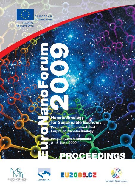
EUR 23733<strong>EuroNanoForum</strong>2009Nanotechnologyfor Sustainable EconomyEuropean and InternationalForum on NanotechnologyPrague (Czech Republic)2 - 5 June 2009PROCEEDINGS
Interested in European research?Research*eu is our monthly magazine keeping you in touch with main developments (results, programmes, events, etc.). It isavailable in English, French, German and Spanish. A free sample copy or free subscription can be obtained from:European CommissionDirectorate-General for ResearchCommunication UnitB-1049 BrusselsFax (32-2) 29-58220E-mail: research-eu@ec.europa.euInternet: http://ec.europa.eu/research/research-euEUROPEAN COMMISSIONDirectorate-General for ResearchDirectorate G - Industrial TechnologiesUnit G.4 - Nano- and converging Sciences and TechnologiesContact: Dr Christos Tokamanis, Dr Sophia FantechiEmail:christos.tokamanis@ec.europa.eusophia.fantechi@ec.europa.euInternet: http://cordis.europa.eu/nanotechnology
EUROPEAN COMMISSION<strong>EuroNanoForum</strong> 2009Nanotechnology for Sustainable EconomyEuropean and International Forum on NanotechnologyEdited by: Sophia Fantechi (Directorate-General for Research, European Commission)Lenka Havlíčková, Eva Svobodová, Rudolf Fryček and Vladimír Albrecht (Technology Centre ASCR)Version 2, July 2009Proceedings of the Forum organized by the Technology Centre of the Academy of Sciences of theCzech Republic, with the support of the Czech Ministry of Education Youth and Sportsand the European Commission, held in Prague on 2-5 June 2009 as an official eventof the Czech Presidency of the Council of the European UnionDirectorate-General for Research2009 Cooperation / Nanosciences, nanotechnologies, materials, and new production technologies EUR 237331
EUROPE DIRECT is a service to help you find answersto your questions about the European UnionFreephone number (*):00 800 6 7 8 9 10 11(*) Certain mobile telephone operators do not allow access to 00 800 numbersor these calls may be billedLEGAL NOTICENeither the European Commission nor any person acting on behalf of the Commission is responsible for the use whichmight be made of the following information.The views expressed in this publication are the sole responsibility of the authors and do not necessarily reflect theviews of the European Commission.A great deal of additional information on the European Union is available on the Internet.It can be accessed through the Europa server (http://europa.eu).Cataloguing data can be found at the end of this publication.Luxembourg: Office for Official Publications of the European Communities, 2009ISBN 978-92-79-12973-5DOI 10.2777/38933© European Communities, 2009Reproduction is authorised provided the source is acknowledged.Printed in Czech Republic2
Acknowledgements<strong>EuroNanoForum</strong> 2009 has been organized by the Technology Centre ASCR with the support of the European Commission and the CzechMinistry for Education Youth and Sports as the fourth conference of a set of international nanotechnology conferences organized within theframework of national Presidencies of the European Union. The 4-day event, held from 2 nd to 5 th of June 2009 at the Prague Congress Centre,has gathered almost 800 participants from 36 countries. Focusing on "Nanotechnology for sustainable economy", <strong>EuroNanoForum</strong> 2009has addressed the state-of-the art of key application areas of nanotechnologies as well as the challenges for nanotechnology research andinnovation to contribute to a sustainable development of the European society, such as the need for reduction in carbon emissions and fossilfuels dependence, the substantial increase in energy demand, pollution control, clean water management and sustainable quality of life of theEuropean citizens. Moreover, the Forum has created a unique opportunity for researchers and industrial experts coming from diverse fields ofscience and technology to meet, discuss and co-operate, and to contribute to the definition of a European nanotechnology strategy after 2009.A large number of colleagues of the European Commission contributed to the success of <strong>EuroNanoForum</strong> 2009, with their suggestions, ideasand exchanges of views.In particular, special thanks go to the Members of the Interservice Group on Nanotechnology for positively supporting this event of high strategicimportance for the Directorate for Industrial Technologies of Directorate-General for Research.We would also like to express gratitude to the Members of the International Advisory Board of ENF2009, the Scientific Committee of ENF2009and the Czech National Advisory Board of the event for all their positive support and inspiring ideas.Thanks go also to the Ministry of Education, Youth and Sports of the Czech Republic and to all the high-level speakers, poster authors,participants and exhibitors, from Europe and the world, for their valuable contribution and active participation in making <strong>EuroNanoForum</strong> 2009a unique event.The EditorsSophia FantechiEuropean CommissionDirectorate-General for ResearchIndustrial Technologies DirectorateNano- and converging sciences and technologies UnitPetra PerutkováLenka HavlíčkováEva SvobodováRudolf FryčekVladimír AlbrechtTechnology Centre ASCR, Czech Republic3
ForewordsThe title of <strong>EuroNanoForum</strong> 2009, i.e. the “Nanotechnology for sustainable economy”is a big challenge for the time being. When preparation of the <strong>EuroNanoForum</strong> 2009started, the very frequent adjective of nanotechnology was „the technology for the21 st century“, i.e. the far reaching time horizon signified the role of nanotechnology.However, in a year time the world has changed considerably and the ENF2009 takesplace in a time of global financial crisis and economic recession. Hence, we wouldlike to overcome the crisis even by employing the already developed potential of thenanotechnology to radically change the technology portfolios.This book of abstracts convincingly indicates the rich potential of nanotechnology:the organizers obtained almost four hundred contributions. They cover verybroad spectrum of scientific problems, applications of nanotechnology for health,environment, eco-and-energy efficient industrial production, for energy productionand storage and for a number of special industrial sectors. They also tackle aboutsocial and environmental safety and deal with “horizontal issues “ like education and communication, organizinginternational research in this particular field etc.While the current potential of nanotechnology is mapped in this book of abstracts, some important achievementsof nanotechnology are demonstrated at the ENF2009 industrial exhibition, which are however reported ina separate catalogue.The ENF2009 is organised by the European Commission and the Technology Centre of the Academy of Sciences inthe framework of the Czech Republic Presidency of the EU Council.The organizing parties believe, that the ENF2009 scientific programme with its many plenary discussions andcomplemented by several concomitant workshops and the industrial exhibition will create a good platform forefficient contributing to find common ground for solving important problems of our time.Miroslava KopicováMinister of Education, Youth and Sports4
I am pleased to present you <strong>EuroNanoForum</strong> 2009, an official event of the Czechpresidency of the EU and the fourth international nanotechnology conferencesupported by the European Commission.More than ever, in times of global economic and financial crisis, nanotechnology canoffer a boost to promising new business opportunities for industries and investors, andbe a source of sustainable growth and new jobs.The current crisis has put sustainability even more strongly on the agenda and thisis why the leading theme of <strong>EuroNanoForum</strong> 2009 - “Nanotechnology for SustainableEconomy” - is particularly well chosen. The conference will focus on the contributionof nanotechnology research towards reducing carbon emissions and fossil fueldependence; enhancing our material and manufacturing sustainability; improvingpollution control, clean water management and environmental quality; as well assustainable healthcare.And focus on putting European R&D at the service of sustainable development is essential. Not only for our futurein general, is it also essential for the future of research itself. Why? Because it is only if the value of research isunderstood and appreciated by citizens that policy makers will find the support and legitimacy to raise the levelof public research funding. Whether individuals have hopes or fears about what the future will bring, researchand the knowledge and technology it generates, has a role in helping realise those hopes or lessen those fears.This is true more than ever within the development of nanotechnologies. If we want to preserve Europe’s leadingposition in nanotechnology and exploit its full potential, we must make sure that applications are developedsafely and responsibly, taking all societal concerns and implications into consideration.<strong>EuroNanoForum</strong> engages all those involved in the development of nanotechnologies to act responsibly throughan international, open and transparent dialogue. In this endeavour, each of us has a contribution to make.With this in mind, for the organisers and participants of <strong>EuroNanoForum</strong> 2009, and to all those engaged inresearch, development and industrial innovation in nanotechnology go my best wishes for a fruitful and mostsuccessful conference.Janez PotočnikEuropean Commissioner for Science and Research5
Table of contentsAcknowledgements 3Forewords 4Topic: Opening Session 8Topic: Plenary Session 1 - Nanotechnology and sustainable growth 10Topic: Plenary Session 2 - Eco-& Energy-efficient industrial production 12Topic: Plenary Session 3 - Nanotechnology for Energy and Environment 14Topic: Plenary Session 4 - Nanotechnology applications for sustainable health care 17Topic: Plenary Session 5 - Prospects for industrial nanotechnologies 18Topic: Plenary Session 6 - Integrated, safe and responsible nanotechnology governance in the EU 21Parallel Session A1 - Nanotechnology in Eco-& Energy-efficient industrial production - Sustainable production of Chemicals 24Parallel Session A2 - Nanotechnology in Eco-& Energy-efficient industrial production - Applications in construction 25Parallel Session A3 - Nanotechnology for energy - Nanotechnology for H2 production & Storage; Fuel cells 28Parallel Session A4 - Nanotechnology for health and environment - Nanotechnology in pollution monitoring and remediation 30Parallel Session A5 - Future industrial technologies - Bionanotechnology 33Parallel Session A6 - Future industrial technologies - Supramolecular chemistry - Molecular electronics 37Parallel Session B1 - Nanotechnology in Eco-& Energy-efficient industrial production - Applications in transportation 42Parallel Session B2 - Nanotechnology for energy - Photovoltaics and Thermoelectrics 46Parallel Session B3 - Nanotechnology for health and environment - Nanotechnology applications for water treatment 49Parallel Session B4 - Nanotechnology for Health and Environment - Bio non-bio interfaces in medical applications 52Parallel Session B5 - Horizontal activities - Safety, environmental and health protection, LCA 55Parallel Session B6 - Horizontal activities - Nanoengineering: from nanostructure characterisation to processing technologies 58Parallel Session C1 - Nanotechnology in Eco-& Energy-efficient industrial production - Applications in textile industry 61Parallel Session C2 - Future industrial technologies - Nanophotonics, (O)LEDS 65Parallel Session C3 - Nanotechnology in Eco- & Energy-efficient industrial production - Nanotechnology in food and other consumer products 67Parallel Session C4 - Future industrial technologies - Nanotechnology based materials 68Parallel Session D1 - Nanotechnology in Eco-& Energy-efficient industrial production - Nanomanufacturing 71Parallel Session D2 - Future industrial technologies - Nanoelectronics 73Parallel Session D3 - Nanotechnology for Health and Environment - Nanomedicine - drug delivery 75Parallel Session D4 - Future industrial technologies - Polymer nanocomposites & membranes 78Parallel Session E1 - Nanotechnology for energy - Rechargeable batteries; Supercapacitors 82Parallel Session E2 - Nanotechnology for Health and Environment - Nanomedicine - diagnostics 84Parallel Session E3 - Horizontal activities - Standardization 87Parallel Session E4 - Horizontal activities - ELSA 90Parallel Session E5 - Horizontal activities - From national initiatives to integrating activities - Roadmap to paneuropean funding 92Parallel Session E6 - Horizontal activities - Education 95Parallel Session E7 - Horizontal activities - European Technology Platforms 98Poster Session 1 - Nanotechnology in Eco- & Energy-efficient industrial production 99Poster Session 2 - Nanotechnology for energy 103Poster Session 3 - Nanotechnology for health and environment 111Poster Session 4 - Future industrial technologies 146Poster Session 5 - Horizontal activities 185Poster Session 6 - Late abstracts 201Authors´s index 272Conclusions 278Organisation management 279Annex I - Final programme 281Annex II - Exhibitors catalogue 309Practical information 3247
Topic: Opening SessionNanotechnologies: Their Promise for Sustainable DevelopmentMr José Manuel Silva Rodríguez 11Director-General for ResearchEurope has the goal of becoming a competitive, knowledge-based economy, without neglecting the social and environmental sides.Nanotechnology is crucial for the improvement of Europe’s competitiveness and the quality of life of its citizens.The financial crisis has made the Commission put in place a recovery plan that also will be a forward looking investment acknowledging that thecompetitiveness of Europe depends on its potential for innovation.Nanotechnology is a good example of this due to its potential to lead to applications that benefit both European society and the Europeaneconomy, promoting sustainability. Some of these applications are with us today; others are at an advanced research stage; and others showpromise for the longer term.Successive EU Framework Programmes for Research and national programmes have committed billions to research in nanotechnology. Resultsare already evident in four broad application areas: Materials and manufacturing; Information and Communication Technologies; Energy andEnvironment; and Health.Nanotechnology is already improving materials and surfaces, increasing the value of existing products. Nanoelectronics is improving our livesand advances in this large field are providing opportunities for growth and improving quality of life - just as microelectronics has done before it.Most importantly will nanotechnologies make valuable contributions to sustainability, thanks to savings in energy and resources. Bothmanufacturing and chemistry can become cleaner through the use of new methods based on nanotechnology.Another promising topic, also covered at this conference is Nanomedicine or the application of nanotechnology to health. Nanomedicine offersmany possibilities to improve diagnosis and therapy. It can tackle serious diseases, and it can make medical care both more effective and moreaffordable for society.The benefits of nanotechnology to sustainability are expected to increase as converging sciences and technologies enable radical rather thanincremental progress in research.Under the 6 th Framework Programme (FP6), almost 1.4 billion EUR of funding was invested in total. More than 550 projects were fundedinvolving nanosciences and nanotechnologies. Over its lifetime, FP6 accounted for almost a third of total public expenditure in Europe in thisarea. FP6 has seen increasing industrial participation in nanotechnology projects. Also, the creation of several European Technology Platformshas strengthened public-private cooperation.The 7 th Framework Programme is already leading to further progress, with almost a billion EUR invested in the first two years alone. And thisdoes not include the large national investments.Of course, nanotechnology raises the issue of safety. Human health and the environment must be protected. And ethical principles must berespected.The Commission takes these issues seriously. It is working to ensure that the public can benefit from the innovations that nanotechnologies maybring, while being protected from any adverse impacts. Research efforts on human and environmental safety has seen nearly 50 MEUR alreadycommitted in this area between 2004 and 2008. It is expected that the total budget committed in Europe will increase, reaching a figure of atleast 100 MEUR by 2013, thanks to FP7 and the corresponding investments of Member States.To address ethical issues, the Commission made a Recommendation on a Code of Conduct for nanotechnology research. This is a voluntaryCode of Conduct aiming to promote safe and responsible nanotechnology research; and pave the way for its safe and responsible applicationand use.That said, we must not forget that private investment is lagging behind public investment. It is important that industrial participation andindustrial funding should increase.In reaping the rewards of nanotechnology we must make sure that excellent research is translated into tangible benefits. And we must makesure that applications are not brought about without a meaningful involvement of society. The Nanotechnology Action Plan (2005-2009) hasserved us well in supporting Europe’s integrated, safe and responsible approach and we intend to continue this line.With this outline of the promise of nanotechnology, and how European efforts to boost research capacity can and should work together, for theultimate benefit of European society and European industry, I trust that this event will be successful in presenting the achievements and furtherpromise of nanotechnology for sustainable growth.8
Sustainability in the 21 st Century and the role of Nanoscience and NanotechnologyH. Kroto 11Francis Eppes Professor of Chemistry, Florida State University, Tallahassee, USAOur modern world is precariously balanced on Science, Engineering and Technology (SET); an understanding of these disciplines is vital by all inpositions of significant responsibility . Although wisedecision-making may not be guaranteed by knowledge, common sense suggests that wisdom is not a likely consequence of ignorance.SET have revolutionised our lives and there is no doubt that humanitarian contributions have improved the quality of life in the developedworld immeasurably. These improvements were brought about byscientific/technological advances based on doubt and questioning - evidence dependent philosophies totally at variance with the belief-basedconcepts that underpin all mystical societal attitudes.Society has the power to use technology so that it can be of benefit or be detrimental. Political decisions have resulted in the existence of some28,000 nuclear weapons worldwide; in addition it appears that our technologies may have catalysed a mindless plundering of the Planet’sresources. We may be hurtling towards disaster - we may not need an asteroid.For a 50:50 chance of surviving into the next century, every segment of society, from industrialists, engineers and scientists to politicians, farmersand fishermen must recognise that these issues are the most serious that the human race has ever confronted. Our only hope for survival restson the shoulders of those who take survival and sustainability issues seriously - and do something about it.I see a key role for “Nanoscience and Nanotechnology”, where Chemistry overlaps Condensed Matter Physics, Molecular Biology and MaterialsEngineering. Improved SET education is also vital.We have manifestly failed in this endeavour but there may be one last hope: The Internet is a major new communications technology which wemust exploit to educate people on a global scale in the rational attitudes to decision-making that are now vital to our very survival.9
Plenary SessionsTopic: Plenary Session 1 - Nanotechnology and sustainable growthPL-01Sustainable development: a challenge for nanotechnologyP. Krüger 11Bayer MaterialScience AG, Leverkusen, GermanyNanotechnology (NT) is in general considered as one of the key enabling technologies in the 21 st century. Extreme high market volumes andgrowth rates were predicted by a multitude of market studies for NT enabled products and applications.On the other hand side today’s society is faced with many essential challenges with respect to the protection of climate and environment fortomorrow’s generations.Especially there is a strong need to find new technology options for the conversion, storage and efficient use of energy, to provide commerciallyviable solutions for a reliable power supply in the future. This is required among others for a significantly reduced level of CO2-emissions, astargeted worldwide in many governmental programs and declarations, to avoid or at least mitigate a serious climate change.The efficient use of in general limited resources also besides of energy, such as water and raw materials as well as the prevention contaminationshave to be also an essential element of next technology generations. Technologies for the remediation of air, water and soil will also becomeimportant to recover the heavily used environment.Since NT is a versatile enabling platform with a wide impact on different fields of materials, processes and applications, it can be utilized to gainmany different kind of sustainable solution options to protect or recover our environment, climate and to improve the quality of our life.The close and intensive cooperation of academia, industry, politics as well as of other stakeholders in the society is urgently needed, to transferexcellent nano science to inventions and finally to nano based innovations. These innovations are basis for commercially viable sustainableproducts and processes along the value chain on a long time scale. Such innovation based incrementally improved or disruptive products andapplications will also sustainably secure the position of European countries in the world wide economic competition in the future.For the long term success of a sustainable NT to sustain our environment and climate as well as to improve our life the responsible safe handlingand use of NT based innovations (e.g. such as nanomaterials and processes) has to be ensured This includes research on health and environmentrelated topics, taking also care of potential exposure routs as well as considerations of the life cycle aspects.This means that research for safety has to be an integral part of the NT based innovation strategy.PL-02Nanotechnology Commercialization: Stealth Success, Broad ImpactM.M. Nordan 11Lux Research Inc., New York, USANanotechnology is not an industry or a sector - it’s a general-purpose toolkit that’s contributing to product innovation in virtually every fieldof manufactured good. Emerging nanotechnology enabled nearly $250 billion in products in 2008, on track to exceed $3 trillion in 2015, butthe vast majority of the applications - in fields ranging from automotive composites to battery electrodes - are never referred to with “nano”terminology. Nanotechnology’s impact will be broad and pervasive, but will not define new clusters of economic activity - more like theassembly line than recombinant DNA. This talk will review the current status of nanotechnology commercialization and describe a ten-yearfuture outlook based on Lux Research’s continuous technology scouting in the field.PL-25Nanotechnology and the Future of Information TechnologyW. Riess 11IBM Research GmbH, Zurich Research Laboratory, SwitzerlandScaling of semiconductor technology (CMOS) has been the driving force for the success of information technology. However, as devicedimensions continue to shrink into the nanometer length-scale regime, conventional semiconductor technology will be approachingfundamental physical limits. New strategies, including the use of novel materials and 1D-device concepts, innovative device architectures, andsmart integration schemes need to be explored and assessed. They are crucial to extend current capabilities and maintain momentum beyondthe end of the technology roadmap time frame (post-CMOS era).10
Plenary SessionsPL-03From research to nanotechnology business - a case study: the Nanochallenge initiativeN. Trevisan 11Veneto Nanotech Scpa, The Italian Cluster of Nanotechnologies, Padova, ItalyNanochallenge is an international business plan competition for business ideas in nanotechnology.The competition aims at funding high-tech start-ups and at soliciting funds from early stage investors and venture capital firms.A total amount of € 600.000 will be awarded at the 2009 Competition Final Contest. The winner of the nanotechnology Grand Prize will receive €300.000.The competition is organized by Veneto Nanotech - the Italian Cluster for Nanotechnology, that was founded in 2003 by the Italian Ministryfor University and Research and by the Veneto Region (north-east Italy). Nanotechnology research in Veneto is very advanced. More than 600Professors, Researchers and PhD Candidates are employed in local Universities and Research Centers. Such concentration of competences canalso count on a series of links and collaborations with international Universities and Research Institutes.In addition Veneto Nanotech activities include:Development of facilities and technology transfer.Education, training and dissemination.Support of new entrepreneurship.Innovation can be a bottom-up process. The program designed by Veneto Nanotech in 2005 to support new start-ups was Nanochallenge,a business plan competition which every year awards a seed capital investment of 300 K€ to the best business idea based on nanotechnologyand since 2007, polymerchallenge offers 300 K€ to best idea on polymer-based materials. Thanks to this initiative eight new enterprises havebeen founded so far. The competition attracts scientists, researchers and entrepreneurs from all over the world, that every year apply tocompete.Nanochallenge aims at:Creating start-ups within the technological clusters.Creating a network among research, financial and entrepreneurial worlds.Transferring innovation in existing enterprises, by presenting nanotechnology projects to be applied to their technologies or their products.Attracting the best scientific talents.Boosting private investments in research and high-tech business.The 300 K€ is divided into 200 k€ in cash and 100 K€ in services which comprise: access to Veneto Nanotech facilities and structures, use of toolsand machineries, office spaces, legal support, commercial and marketing assistance, networking with venture capitalists and business angels fora second round of investments.Since 2005 Nanochallenge has become a successful brand bringing the following results:Total prize 2005-2007: 1,8 M EURO, Investments moved: 20 M EURO, Number of start-ups created: 8, Jobs created: 25, Applications received: 145,Countries of origin of the teams: 25, National and international fi nalist teams: 67, International scientists hosted for the Final Contest: 157,Venture capitalists involved in the jury: 15 of whom 5 Italians, 6 Europeans, 4 from USAPL-27Nano-Bio-Info-Cognitive sciences - the base of a new convergent NBIC technologyMikhail Kovalchuk 11General Director, Kurchatov Insitute, RussiaThe main direction of technological evolution is synergetic integration (or converging) of four technologies: nanotechnologies, biotechnologies,including genetic engineering and protein crystallography, information technologies and neuro-cognitive technologies. This is a new trend inscientific development -nano-bio-info-cognitive technologies - NBIC technologies.NBIC-technologies formation opens possibility for creation a new hybrid nanomaterials, nanosystems and nanodevices, combining advantagesof living and non-living nature.In particular we have in mind development of• biosensors, biochips and hybrid sensors on their basis;• neuro-electronic systems for interaction of human brain with computer and another technical systems;• bio- and antropomorphous roboto-technical arrangements and systems, etcIn the presentation the main points of developing the research and technological infrastructure at interdisciplinary “Kurchatov NBICcenter” for nano-bio science and convergent technologies, based on dedicated synchrotron radiation source, research neutron reactor andsupercomputer center are introduced.11
Plenary SessionsTopic: Plenary Session 2 - Eco-& Energy-efficient industrial productionPL-04Make Money by Nano and respect Eco-and Energy efficiency? Nano based products in construction,cleaning, health, cosmetics and other industriesA.E. Reinhardt 11microTEC, Bad Dürkheim, GermanyIn its first part the presentation shows an overview how nanotechnologies support sustainable production and a new generation of high valueproducts. The samples presented cover very different fields, e.g. construction, cosmetics, health. By explaining realized applications of latest R&Dresults in their different markets it is aimed to inspire the discussion how in future nano related research will be faster then ever before part ofbusiness strategies towards products offering parallel fast return of investment, respect eco- and energy efficiency in the whole life cycle of theproduct and are oriented towards the main goal: bring benefit to the people and rescue the competitiveness of Europe. In its second part thepresentation opens the way to tools for building contacts in Europe, start cooperative R&D projects and disseminate the results cost efficient viaservices like cordis wire, business- and social networks like xing, twitter, eunanopaprika and others.PL-05Nanotechnology in sustainable chemical productionM. Pridöhl 11Evonik Degussa GmbH, Hanau, GermanyTechnical processes in the chemical industry often require high energy input. On average 10% of the operating costs in chemistry are related toenergy. The energy costs for producing large volume base chemicals reach up to 40%, making the chemical industry to one of the most energyconsuming sectors. Therefore continious improvement of energy efficiency is a top priority.Promising concepts to improve the energy efficiency are microreactors with increased heat and mass transport, innovative rection media likeionic liquids, new methods for selective and targeted enegy input and measures to increase yield, product concentration and selectivity ofexisiting processes.A key role in this context play catalysts. More than 80% of all chemicals products are produced with support of a catalyst. Catalyst lower theactivation energy respectively the reaction temperatures, improve selectivity and yield and reduce waste streams. Thus new and improvedcatalysts are essential for further improving the energy efficiency of chemical processes.The interest in nanomaterials and metal nanoparticles (NPs) as catalysts is increasing dramatically, as reflected by the large number ofpublications in the last years. Over 80 related articles have been published just in the last 5 months. Industrial relevant examples as the directsynthesis of hydrogen peroxide will be discussed. 1A related but brand new research topic are superparamagnetic nanoparticles acting as heterogeneous catalyst and additionally as energysource for chemical synthesis. These catalysts heat up in electromagnetic fields and provide the activation energy selectively at the catalystsurface improving energy efficiency, turnover rate and process speed. 2The concept of selectively introducing energy by means of superparamagnetic particles can also be used to speed up technical processes likebonding and polymerization. 3Coatings against biofouling 4 and improved thermoelectric materials are other promising developments of nanotechnology. Nano-structuredcoatings may help to maintain the efficiency of heat exchangers. Nanostructuring greatly improved the performance of thermoelectric materialsin the last years. This may allow to economically generate electrical power from waste heat and low temperature sources. 5[1] Jennifer K. Edwards and Graham J. Hutchings, Angew. Chem. Int. Ed. 2008, 47, 9192 - 9198[2] S. Ceylan, C. Friese, C. Lammel, K. Mazac, A. Kirschning, Angew. Chem. Int. Ed. 2008, 47, 8950 -8953[3] http://www.nanowerk.com/news/newsid=687.php[4] AMBIO, Integrated EU FP6 project[5] J. Sootsman, H. Kong, C. Uher, J. D_Angelo, Chun-I Wu, T. Hogan, T. Caillat, M. Kanatzidis, Angew. Chem. Int. Ed. 2008, 47, 8618 -862212
Plenary SessionsPL-06Energy efficiency in buildings: opportunities for sustainable innovations and the role of the E2BAssociation to make them happenS. Carosio 11D’Appolonia S.p.A., ItalyThe objective of the presentation is to provide an overview of the strategy that is being implemented at European level concerning energyefficiency in new and existing buildings (including cultural heritage). In this framework the European Association for Energy Efficiency inBuildings (E2BA) will be introduced, being an industry lead European Initiative grouping all the stakeholders in the value chain to work closelywith the European Commission within an effective Public Private Partnership (EeB PPP). The EeB PPP is fostering the development and largescale demonstration of novel multidisciplinary solutions enabled, among the others, by nanotechnology and new materials. Some exampleson how nano-technology could contribute to this paradigm shift will be shortly presented. In particular the use of nano-structured catalyticcoatings in next generations of water electrolysers and hydrogen burners will be discussed, providing some insights concerning their use incombination with Renewable Energy Sources in buildings and districts of buildings.PL-07Nanotechnologies Enabling Clean and Energy Saving mobilityV. Lambertini 11Centro Ricerche Fiat, Micro and Nanotechnologies Department, Orbassano, ItalyThe automotive industry is one of the largest demanding areas of materials and technologies to develop sustainable devices with greatimpact on safety, on-board well-being, environment compatibility and fuel saving. Since the mid nineties the potential applications of microand nanotechnology in the automotive has been demonstrated practically in all systems and subsystems from the tyres to the roof and fromthe headlamps to the tail lamps. In 10 years, the design and manufacturing of cars will be significantly affected by nanotechnology appliedto 70% of automotive applications with expected market $6.46 billion (Frost & Sullivan). During the first decade of quite intense R&D, micronanotechnologycontributed to enhanced safety and comfort, but their main impact has been on the reduction of fuel consumption, noxiousand green house gas emissions. The developments of new propulsion systems and the applications of nano catalysis for gasoline, dieseland natural gas systems can be considered the most relevant on energy saving and public health. All automotive manufacturers have spentconsiderable resources so that in spite that most car segments increased in size, weight and power, the overall consumes and emissions havedecreased.The evolutionary approach aiming at the use of micro nanotechnologies to enhance the current mobility based on Internal Combustion Engineswill continue for several years, but we are now being confronted with the original expectation, micro-nano technologies as the enablers of thecleanest and the most effective energy savings form of mobility: the electrical vehicle.With respect to the conventional road mobility based on Internal Combustion Engine cars, the major benefits related to the introduction ofthe full electrical mobility are: savings of the primary energy currently used in transportation (30-40% when the electricity is produced by theconventional thermoelectrical plants and up to 60% when the electricity is produced by renewable sources), reduction of green house emissions(40-50% if the electricity would be produced by the current European mix, and 10-15 times if the electricity would be produced by renewables)and zero local emissions of noxious emissions such as NOx, SOx and fine particles.The availability of the state-of-the-art nanomaterials and micro-nano technologies is essential, but in this brief overview we emphasise that,when dealing with a complex product like an automobile, the success is determined by advanced sub-systems design and integration aiming atthe optimisation first of the major system blocks then at the vehicle as a whole. The major system blocks enabling high performance necessaryin the forthcoming electrical mobility are shown in figure around PHYLLA, the Centro Ricerche Fiat mobile laboratory to support the researchand industrial developments on Electrical Vehicles of the Fiat Group.13
Plenary SessionsTopic: Plenary Session 3 - Nanotechnology for Energy and EnvironmentPL-08Catalytic model systems studied by high-resolution, video-rate Scanning Tunneling MicroscopyF. Besenbacher 11Aarhus University, Interdisciplinary Nanoscience Center, Aarhus, DenmarkDeveloping renewable, sustainable and green energy resources and securing the environment by reducing the emission pollutants are two ofthe largest challenges for the human civilization within the next 50 years. Besides the well-known energy resources that power the world today,petroleum, coal, and natural gas, active research and development is done exploring alternative energy resources such as solar, biomass, wind,and hydrogen.To realize the vision of a clean society and our vision of plentiful, low cost sustainable energy, research and innovation within the area of therapidly expanding fields of nanoscience and nanotechnology, multi-disciplinary by nature involving physics, chemistry, biology, molecularbiology, is mandatory. For decades single-crystal surfaces have been studied under ultra-high vacuum (UHV) conditions as model systems forelementary surface processes. This “surface science approach” has contributed substantially to our understanding of the processes involved inespecially catalysis.In this talk I will show how Scanning Tunneling Microscopy (STM) can reveal fundamental processes in relation to catalysis, and how we canextract quantitative information on surface diffusion of adatoms and molecules [2-4]; diffusion of vacancies; interstitials and molecules, e.g.water molecules on oxide surfaces [5, 6, 7]; sintering and diffusion of nanoclusters on oxide surfaces [7]; diffusion of intermediate species [8-10]; identification of active sites and determination of new nanostructures with novel, catalytic properties from time-resolved, high-resolutionSTM images/movies (see www.phys.au.dk/spm) [1]. The atomic-scale information obtained may even lead to the design of new and improvedcatalysts in certain cases [11-12].References[1] F. Besenbacher, Reports on Progress in Physics 59, 1737 (1996)[2] T. Linderoth et al. Phys. Rev. Lett. 78, 4978 (1997)[3] S. Horch et al., Nature 398, 1344 (1999)[4] Roberto et al. Nature Materials, Nature Materials 3, 779 (2004)[5] R. Schaub et al., Science 299, 378 (2003); Science 303, 511 (2004)[6] S. Wendt et al., Physical Review Letters 96, 066107 (2006)[7] S. Wendt et al. Science 320, 1755 (2008)[8] D. Matthey, et al., Science 315, 1692 (2007) .[9] E. Kruse Vestergaard et al., Phys. Rev. Lett. 88, 259601 (2002)[10] J. V. Lauritsen et al., J. Catal. 197 1-5 (2001)[11] J. Kibsgaard et al, Journal of the American Chemical Society, 128, 13950 (2006).[12] F. Besenbacher et al., Science 279, 1913 (1998).14
Plenary SessionsPL-24Functionalized Nanomaterials for Solar Power Conversion and StorageM. Graetzel 11Ecole polytechnique fédérale de Lausanne, Lausanne, SwitzerlandThe quality of human life depends to a large degree on the availability of energy sources. As a consequence of dwindling fossil resources andenhanced energy consumption due to the growth of the world population, a huge power supply gap of 14 terawatts, equaling today’s entireconsumption is expected to open up by year 2050.Nanotechnology is expected to make important contributions to identify environmentally friendly solutions of the energy supply problemthe world is facing. The sun provides about 100’000 terawatts to the earth which amounts to six thousand times the present rate of the world’senergy consumption, Learning from the concepts used by green plants we have developed a molecular photovoltaic device whose overallefficiency for solar energy conversion to electricity has already attained 12.2 %. The new solar cell is based on the sensitization of nanocrystallinetitanium dioxide films by a molecular dye [1-3]. The underlying fundamental processes of light harvesting by the sensitizer, ultrafast electrontransfer from the electronically excited dye into the conduction band of the semiconductor oxide and the transport of the injected electronsthrough the mesoporous film to the collector electrode will be analyzed in my lecture. The low cost and ease of production of the new cellshould benefit large-scale applications. Impressive stability both under long-term light soaking and high temperature stress has been reachedfostering first industrial applications. These systems will promote the acceptance of renewable energy technologies, not least by setting newstandards of convenience and economy.The lecture will also report on most recent progress in the use of nanotechnology for electric power storage in secondary lithium ion batteries.References:[1] B. O’Regan and M. Grätzel “A Low Cost, High Efficiency Solar Cell “ Nature, London 353, 1991.[2] U.Bach, D.Lupo, P.Comte, J.E.Moser, F.Weissörtel, J.Salbeck, H.Spreitzert and M.Grätzel, “SolidState Dye Sensitized Cell Showing High Photon to Current Conversion Efficiencies” Nature, 395,550 (1998).[3] M Grätzel , “Photoelectrochemical Cells” Nature 414, 338−344 (2001).PL-09The role of atmospheric nano-particles in climate forcingJ.P. Putaud 11European Commission, Joint Research Centre, Institute for Environment and Sustainability, Ispra, ItalyThe average number concentration of particles in the lower atmosphere ranges from ca. 1000 to 100,000 cm -3 across Europe. Most of theseparticles have a diameter smaller than 100 nm (nano-particles). Some are from natural origin (sea spray, volcanic, desert dust, biogenic particles),most result from combustion processes (e.g. soot particles from Diesel engines, particles formed in the atmosphere from gaseous pollutants),and very few are engineered nano-particles across Europe. Most of these particles have a diameter smaller than 100 nm (nano-particles). Someare from natural origin (sea spray, volcanic, desert dust, biogenic particles), most result from combustion processes (e.g. soot particles fromDiesel engines, particles formed in the atmosphere from gaseous pollutants), and very few are engineered nano-particles.Atmospheric particles (also called aerosols) directly affect the Earth radiative budget by absorbing or scattering back to space a fraction of thesolar radiation. Atmospheric particles also control the albedo and the lifetime of low stratiform clouds. Climate model simulations suggest thatthe global effect of aerosols is to cool the Earth. This cooling effect might have partly compensated the warming effect due to the increase ofgreenhouse gas concentrations over the industrial era.However, atmospheric particles (also named as PM 10, PM 2.5, etc…) are thought to be harmful to human health. As a consequence, air qualitydirectives set more and more stringent limits for particle emissions and atmospheric concentrations all over the world. It is therefore expectedthat the concentration of atmospheric particles will strongly decrease over the next decades.While efforts for improving air quality should undoubtedly be pursued, the consequences of air pollution abatement policies on climatechange should however not be ignored. Determining how much is the current cooling effect of aerosols is actually essential for forecastinghow much will be the global temperature increase during the next century. This is far more difficult than calculating the warming effectof greenhouse gases due to the great variety in size and nature of the atmospheric particles, to the complexity of the processes involved(interaction light/particles, cloud droplet formation and evaporation) and to the large spatial and temporal variations in aerosol concentrations.The uncertainties of the current aerosol climate effect may be reduced by measuring atmospheric particles’ optical properties and cloud dropletformation potential, together with some more fundamental characteristics (size distribution, chemical composition). Efforts are also beingmade to improve the representation of the role of aerosols in global climate modelling, for a more robust prediction of future temperature andprecipitation fields.15
Plenary SessionsPL-10Getting the good stuff and avoiding the bad: Government’s role in maximizing environmentalbenefits and avoiding unintended consequences of nanotechnologyK. Markey 11United States Environmental Protection Agency, New Chemicals Program, Washington, USAThe United States Environmental Protection Agency (USEPA) regulates the manufacture and use of industrial chemicals to avoid unreasonablerisks to human health and the environment, while also promoting new technologies that have the potential to address environmentalchallenges. Nanoscale materials are a technological platform to achieve these benefits, provided the implications are appropriately managed.However, identifying the implications and avoiding additional unintended consequences is challenging, because many of the risk assessmenttools that have served to identify concerns in previous decades of chemicals management no longer hold for nanoscale materials. At the sametime, there are tangible environmental benefits to be realized. Hence, maximizing the benefits while avoiding the down sides requires judiciouschoices to utilize existing tools, while, where necessary, developing new ones. Central to achieving this balanceis an approach that measures theimplications and benefits of nanoscale materials throughout their life cycles and institutes policies to foster continuous improvements. To thoseends, the Agency has multiple interacting initiatives and programs on nanotechnology to coordinate research, develop testing, collect data, andevaluate results. By considering the overall picture, the Agency is able to prioritize filling data gaps and developing new technologies. Specificcase studies will examine how these different programs interact, how the long-term foundations of economic and environmental sustainabilityof nanotechnology are being achieved, and where future opportunities may lay.16
Plenary SessionsTopic: Plenary Session 4 - Nanotechnology applications for sustainablehealth carePL-11Nanotechnologies in regenerative medicineE. Syková 11Institute of Experimental Medicine Academy of Sciences of the Czech Republic, Department of Neuroscience and Center for Cell Therapy and TissueRepair Charles University, Prague, Czech RepublicMagnetic resonance imaging provides a noninvasive method to study the fate of transplanted cells in vivo. The migration and fate of rat fetalcells, mouse and human embryonic stem cells, rat and human mesenchymal stem cells, rat and human olfactory glia, beta-cells of the isletsof Langerhans or chondrocytes, labeled with superparamagnetic iron-oxide nanoparticles and grafted in animal models of stroke, spinal cordinjury, diabetes or cartilage damage, were studied to elucidate whether these cells are capable of survival, do not produce tumors, differentiate,prevent scar formation and enhance regeneration. Various nanoparticles were developed and patented in our Center for experimental andclinical use.Various biocompatible scaffolds based on non-woven nanofibres (products of ELMARCO or Technical University Liberec), have beendeveloped for bridging tissue defects and for use as 3D stem cell carriers. We use nanofibre constructs seeded with stem cells labeled withsuperparamagnetic iron-oxide nanoparticles to bridge a spinal cord lesion. Our studies demonstrate that nanofibre scaffolds seeded with adultor embryonic stem cells can bridge a lesion site in the brain as well as in the spinal cord. Such constructs are also useful for cartilage repair.We implanted blocks of nanofiber scaffolds, either alone or seeded with MSCs, in order to bridge post-traumatic cavities in injured spinal cord.The nanofibre scaffolds were implanted into rats with acute or chronic SCI. In both acute and chronic SCI, implants reduced scar formation andbridged the lesion, providing a scaffold to reform the tissue structure. Furthermore, nanofiber scaffolds seeded with stem cells can bridge thelesion site and increase functional recovery. We conclude that scaffolds in combination with stem cells can improve regeneration by bridginggaps after SCI, by mechanically supporting ingrowing cells and axons and by the rescue and replacement of local neural cells.PL-12Getting Nanomedicines to Patients - The Therapeutic Nanomedicine PrioritiesM. Eaton 11UCB, Slough, United KingdomIn recent years there has been an increase in research into Nanomedicines but there is industrial concern that much of this effort will not betranslatable in to significant commercial value. Communication between the stakeholders is problematic and much more needs to be done toensure that such funding leads to new drugs for patients. The stakeholders need each other, but currently critical industrial knowledge on drugresearch and development is not readily available to the academic sector. This will be addressed in this talk.The Strategic Research Agenda listed many possible approaches; with the passage of time it is now possible to prioritise these from an industrialperspective. The purpose of a round table meeting in February was to start this process and it is the purpose of this talk to outline the ensuingstrategy, which was further discussed at the ETP General Assembly in Munster. It is hoped that Framework and national funding will be directedto challenging projects, which can be commercialised and offer novel therapeutics to patients.PL-13Application of nanotechnology in medical diagnosticsP. Boisseau 11CEA-LETI, MiNaTec, Grenoble, FranceBy moving from the micron to the nanoscale, nanotechnology enables the development of tools, devices and objects of approximately thesame scale of the biomolecules. This opens a totally new field of application exploiting the interactions between biomolecules and nanodevicesor nanoinstruments.Medical diagnostics covers two main sub-domains: in vitro diagnostics and in vivo diagnostics, including imaging. In both domains,nanotechnologies turn down current limits in terms of technical performances. For instance, in the field of in vitro diagnostics, miniaturisationenables faster interaction between reagents and biomarkers, analysis of smaller samples, better chemical reactivity. In vitro diagnostics goescloser to drug development by proposing tests specific to a new drug.Regarding in vivo imaging, nanoscale contrast agents improve the accuracy, the specificity, the sensitivity and the targeting of biological sites.Hybrid imaging combining different imaging modalities opens new applications in both preclinical and clinical applications. Even some totallynew modalities like magnetic particles imaging are under development.All specific developments in medical diagnostics are driven by clinical applications. Therefore, only multidisciplinary consortia can tackle thesedevelopments.The new horizon open by deep miniaturisation down to the nanoscale reveals new societal, regulatory, and ethical issues to be addressedsimultaneously to the technical development for a harmonious development of these methods. Healthcare policy and more specificallyreimbursement policy will dramatically impact this business as well.17
Plenary SessionsTopic: Plenary Session 5 - Prospects for industrial nanotechnologiesPL-14Characterisation of nanostructures and process technologiesE. Niehuis 11ION-TOF GmbH, Muenster, GermanyIn recent years we have seen impressive progress in nanoscience to manipulate matter on the nanometer scale and to generate nanostructureswith completely new properties and performances. A decisive stimulus for the field was the rapid development of the scanning probetechniques after the invention of the STM by Binnig and Rohrer in 1981. Nowadays these techniques allow not only to see but also tomanipulate single atoms and molecules. In parallel, the more classical analytical techniques based on electron, ion or laser probes have beenimproved considerably with respect to spatial resolution. Therefore, a set of tools has become available to meet the requirements of exploratorynanoscale research.The commercialisation of nanotechnology has just started, and in the future a wide range of innovative nanomaterials, nanostructures anddevices will be introduced to virtually all industrial sectors from Electronics to Medicine. Future nano-manufacturing will critically depend onthe ability to accurately and reproducibly measure properties and compositions on the nanoscale. New process technology developed for theproduction of nanostructures needs to be tailored and monitored in order to meet the demands of efficiency and reliability. This is extremelychallenging for the existing analytical techniques. Instrumentation not only with improved spatial resolution and sensitivity is required, but alsowith significantly higher accuracy, speed, robustness and ease-of-use. The development of the analytical instrumentation to this level will alsorequire global efforts to implement standards and calibration procedures.Access to infrastructure specialised on the characterisation and failure diagnostics for nanodevices will be crucial in particular for the growth ofsmall and medium size nanotech companies. Often a combination of different high-end analytical techniques, sophisticated sample preparationtechniques and a high level of expertise in data interpretation is necessary for problem solving, last but not least together with a fast turnaroundtime. This is a challenge not only for specialised public research centres but also for private analytical service providers. The build-up ofthe required analytical infrastructure and services in Europe is of major importance for the future development of industrial nanotechnology.PL-15Processing-structure-properties in advanced polymer nanocompositesJ.M. Kenny 11University of Perugia, European Centre on Nanostructured Polymers, Terni, ItalyThe ability on modifying and modelling materials at nanoscale level is leading modern society to developments which were unthinkable justa decade ago. For this reason, researchers all over the world have been focused their studies on nanotechnology and nanomaterials: dispersionof even a low concentration of nanoparticles in a material can lead to a drastic enhancement of their performance. Loading of polymers withhigh-aspect-ratio fillers can, in fact, lead to very interesting results regarding the properties of the final composite material, even with a verylow concentration of these particles. Their particular shape and their very high aspect ratio provide a huge specific surface area, which is severalorders of magnitude greater than the one of conventional fillers.Among this kind of fillers, layered silicates, silica, metals, carbon nanoobjects (tubes, fibres, graphenes) have a particular importance in termsof structural behaviour (mechanical properties, thermal and dimensional stability) and also in terms of multifunctional properties (electrical,magnetic, optical, biocompatibility, etc.). As the capacity of nanoparticles of producing materials with excellent properties is strongly related tothe dispersion level attainable, one of the most important challenges is to develop processing method which can ensure an optimal dispersionof the nanoparticles, and, at the same time, can be scaled up at the industrial level.Many techniques have been employed to improve the dispersion of nanoparticles inside the matrix assuring optimum intercalation andexfoliation. Melt processing and in-situ polymerization are the favourite routes while solvent processes are limited to few specific optoelectronicapplications. Most of these techniques, although valid, are limited by their scale up to produce larger amounts of nanocomposite material. Infact, only a technique which allows high rate and high volume production, can be really exploited for industrial applications.Here we present the current state- of- the- art for the processing of polymer nanocomposites for advanced applications. Innovative routes arepresented for the processing of multifunctional polymer nanocomposites with designed mechanical and functional properties allowing thedevelopment of production systems with high reliability. Moreover, the use of nanocomposite matrices to prepare advanced fibre reinforcedcomposites is illustrated. In this case advanced liquid moulding (in particular, vacuum assisted resin transfer moulding -VARTM) can be used tomanufacture epoxy and polyester-based composite laminates for aerospace applications.The development and optimization of advanced processing techniques allowing reliable production methods for well dispersedand homogeneous nanocomposites is on the main research areas whose results are fundamental for the further growth of polymernanotechnologies.18
Plenary SessionsPL-16Nanoelectronics: there plenty of complexity at the bottomL. Baldi 11Numonyx Italy S.r.l. Agrate Brianza, ItalyThe sentence “there is plenty of room at the bottom” appears in a famous talk that Richard Feynman gave on December 29 th 1959 at the annualmeeting of the American Physical Society, and it is generally considered as the first recognition of the potential of Nanotechnology. Feynmanindicated the possibility of printing the entire Encyclopedia Britannica on the head of a pin. In general the talk of Feynman is quoted as anindication of the fact that things could be made much “smaller”. What is usually neglected is that he introduced another factor “complexity”.We are not there yet, however most advanced Flash memory devices can store around 400 thousand pages of text and figures in less than 2 squarecentimeters.Surprisingly enough, and a tribute to the foresight of the man, the main engine of the long evolution that has brought us to 30nm devices hasbeen a sort of photoengraving, based on reverse magnification, as described by Feynman himself.But Nanoelectronics is not only small feature size. Already before entering in the sub-100nm domain, semiconductor devices were exploitingquantum effects, taking place only on the nanometer scale, such as the tunnel effect, used in Flash memories.Unfortunately the same quantum effects that have made Nanoelectronics possible, and have enabled it to enter all aspects of our everydaylife, are also threatening its further evolution. Several factors are concurring to cloud the future of Nanoelectronics: parasitic effects, which arebecoming dominant, change of properties of the matter on the molecular scale, and statistical effects related to large complexity of devices.Even events with a low probability of occurring become almost a certainty when applied to billion of individual elements.The slowing down of the “Moore’s Law” trend, already wrongly announced several times in the past, might be a real risk this time. The reaction ofsemiconductor industry to the new challenge is taking essentially three directions:New materials and new physical mechanisms could overcome some limitations of mainstream technology. The main obstacle is the level ofcomplexity: new technologies must deal with a device count in the order of billions..Smarter design approaches, starting from the high level system architecture down to compensation of unwanted physical effects and statisticalvariation, could increase the efficiency in the utilization of available technology.The already developed technology base can be applied to a much wider field than simple data processing: MEMS, sensors, actuators, optoelectronicdevices, all based on the manufacturing know-how and tools of semiconductor industry are opening the way to new applications andgenerating new industries.As Feynman said: “there is plenty of room at the bottom”.PL-17Prospects in molecular electronics devices based on supramolecular chemistryD. Vuillaume 11CNRS - Institute for Electronics Microelectronics and Nanotechnology, University of Lille - Molecular Nanostructures and Devices group,Villeneuve d’Ascq, FranceMolecular electronics, i.e. the molecule-based information technology at the molecular-scale, becomes more and more investigated andenvisioned as a promising candidate for the nanoelectronics of the future. From this respect, supramolecular assembly of organic moleculeson solid substrates is a powerful “bottom-up” approach for the fabrication of devices for molecular-scale electronics. More than a possibleanswer to ultimate miniaturization problem in nano-electronics, self-assembled molecular electronics is foreseen as a possible and reasonableway to assemble a large numbers of nanoscale objects (molecules, nanoparticules, nanotubes and nanowires) to form new device and circuitarchitectures. It is also an interesting approach to significantly reduce the fabrication costs, as well as the energetical costs of computation,compared to usual semiconductor technologies. Moreover, molecular electronics is a field with a large spectrum of investigations: fromquantum objects, for testing new paradigms, to hybrid molecular-silicon CMOS devices.In this presentation, I will briefly describe the basic concepts related to electron transport through molecules, ensemble of molecules, organicmonolayers and molecular devices mandatory to understand the realistic electron transport in these molecular devices. I will introduce some“supra-molecular technologies” useful to make these organic nano-devices and pinpoint some specific problems encountered when workingwith molecules. I will review some recent results in this field, especially dedicated to the applications towards some information technologyfunctions (e.g. molecular memories, switches, transistors, etc…), and I will discuss some perspectives and challenges.19
Plenary SessionsPL-18Value-added materials: prospects and barriersE. Vandeweert 1 , R. Tomellini 11European Commission, Directorate-General for Research, Industrial Technologies, Value-added materials Unit, Brussels, BelgiumMaterials research has an essential role in supporting development of competitive and sustainable growth in Europe: the globalization of themarkets and the increasing complex needs of society demand improved industrial processes and products with better service performance,quality, reliability, durability, specific functionalities and end-of-life destiny. Industry does not simply “deliver products”, it now also has to playan active role towards an economic development that wants to be responsible and really sustainable, thus facing strategic objectives includingenergy balance, raw materials supply, carbon fingerprint, cost effectiveness, extended/networked manufacturing, safety and environmentalprotection or improvement. At the same time, market trends make it even harder to meet these objectives, as customers look for better andcheaper products, which in many cases should also be small, light and even wearable or portable.The European Commission promotes research in materials science and engineering. The EU 7 th Framework Programme for Research andTechnological Development is currently supporting research actions to overcome scientific, technological and related bottlenecks, provoking orfacilitating new ideas that can give Europe a competitive advantage internationally in the forthcoming years.PL-26Experience in the Field of Research Activities with Universities - Nanotechnologies in CarJ. Machan 1 , R. Stranský 1 , D. Kramer 21Skoda Auto, Czech Republic2VW, GermanyWithin the EU 7 th Framework program (FP7 in 2009 - 2013) it was defined five major topics on the EUCAR level with high importance forautomotive industry.The five of major importance to automotive and road transport research are:• Information and Communication Technologies (ICT)• Nanosciences, Nanotechnologies, Materials and new Production Technologies (NMPT)• Energy• Transport• SecurityNanosciences, Nanotechnologies, Materials and new Production Technologies (NMPT) play role in the following four sectors of automotivereseach areas:• Fuels and Powertrain (Powertrain materials)• Integrated Safety (New materials for crash worthiness)• Virtual Engineering (Methods for design, production)• Material Processes, Manufacturing (Multifunctional materials, Methods and approach for design, process and manufacturing)Taking advantage of using nanomaterials in automotive applications can’t be purposeless. It should follow these aims:• Reduced fuel consumption and emission• Reduced weight• Cost reduction• Energy efficiency• Robust construction and safety applicationsIn automotive applications nanomaterials and nanotechnologies find utilization mainly in the following areas:• Powertrains (lowered friction, increased lifecycle, etc.)• Safety (new materials for crash worthiness)• Exterier, bodywork (scratchresistant and dirtresistant surfaces, etc.)• Interior (scratchresistant surfaces, comfortable materials, noise suppresion, etc.)• Air-condition (biologically inert filters, etc.)• Electro (battery applications, supercapacitors, etc.)This contribution focuses mainly on utilization of nanomaterials in the area of scratchresistant parts construction. Research and development inthis area is done by Skoda Auto a.s. in close cooperation with the Brno University of Technology.20
Plenary SessionsTopic: Plenary Session 6 - Integrated, safe and responsible nanotechnologygovernance in the EUPL-19observatoryNANO - supporting informed decisions on nanotechnology developmentsM. Morisson 11Institute of Nanotechnology, Glasgow, UKNanotechnology is a complex and rapidly changing field, which is often difficult to assess in terms of opportunities, challenges and risks.The observatoryNANO project is funded by the European Commission (EC) under the seventh Framework Programme (FP7) to address this,by providing the EC and other policy and decision makers with reliable information regarding the current and forecasted development ofnanotechnology and its potential impacts on society.It assesses all aspects of the value chain from basic research to market applications in terms of scientific, technological and socio-economicdevelopments and prospects. At the same time it evaluates ethical and societal aspects; potential environment, health and safety issues;and developments in regulations and standards. For the purposes of this work the assessment is performed in ten broad sectors: aerospace,automotive, and transport; agrifood; chemistry and materials; construction; energy; environment; health, medicine, and nanobio; ICT; security;and textiles.The project activities have three main phases (which have an annual cycle):phase 1 is a review phase. Existing literature (peer-reviewed scientific publications, company reports, reports from other projects and initiatives,such as the European Technology Platforms) is collated and analysed, and interim reports produced. At the same time this work is supportedby an analysis of patent trends (using the PATSTAT database and in collaboration with the European Patent Office) and trends in peer-reviewedpublications.phase 2 involves engagement with the wider expert community through invitation to review the interim reports, participation in interviews andworkshops, and completing a series of online questionnaires covering the different technology sectors.phase 3 is publication and dissemination. There is an annual symposium, where outcomes from the review and expert engagement processesare presented; followed by the publication of concise reports, in an online database, which clearly identify developments, opportunities,challenges and risks in each of the technology sectors.At the end of the first year of the project, the following have been published:53 reports on different scientific and technological developments;34 reports on economic impacts;report on individual and collective responsibility for nanotechnology, interviews with key opinion leaders on ethical aspects of nanotechnologydevelopments and a toolkit to support researchers in review of the ethical aspects of their work;review of seminal research in environment, health and safety aspects of nanotechnology developments;review of developments in standards and regulations;review of existing and proposed observational initiatives.About the observatoryNANO projectThe project is led by the Institute of Nanotechnology (IoN) (UK), and includes: VDI Technologiezentrum (DE), Commissariat à l’énergie atomique(CEA) (FR), Institute of Occupational Medicine (IOM) (UK), Malsch TechnoValuation (MTV) (NL), triple innova (DE), Spinverse (FI), Bax and WillemsConsulting Venturing (B&W) (ES), Dutch National Institute for Public Health and the Environment (RIVM) (NL), Technical University of Darmstadt(TUD) (DE), Associazione Italiana per la Ricerca Industriale (AIRI) (IT), Nano and Micro Technology Consulting (NMTC) (DE), Swiss FederalLaboratories for Materials Testing and Research (EMPA) (CH), University of Aarhus (DK), MERIT - Universiteit Maastricht (NL), Technology CentreAS CR (CR).For further information please contact the project coordinator Dr Mark Morrison (mark.morrison@nano.org.uk)or visit the project website: www.observatory-nano.euobservatoryNANO is funded by the European Union under FP7. Contract number 218528.21
Plenary SessionsPL- 20European Technology Platforms - Responsible development of Industrial NanotechnologiesP. Matteazzi 11MBN Nanomaterialia, ItalyIn the last decades Nanotechnology has passed from science fiction to niche research to advanced technology and finally to industrialproduction. Now Nanotechnologies are ready to adds new functionalities, intelligence, integrations, portability and networking capability inmany new products with high market potential in several industrial sectors.The many benefits of Nanotechnologies have to acquire strategic significance and they would have to be weighed against the risks involved(safety, economical/market impact, industrial sustainability, environment, ethical and political issues). Therefore the European policy onNanotechnology innovation has to be promoted and developed to be of the same standard as other no-research issue , i.e. regulatory andeducational.Advanced nano and microfabrication are exciting not only from the environmental aspect (fewer energy and resources will be consumed oncethese technologies mature) but also from economic side. Their capabilities are becoming key enablers for gaining or maintaining the lead overcompetitors in order to sustain a strong economy and provide an impetus towards meeting societal demands.To respond to a even wider interdependent interests constituted not only by industrial needs, but also by ETPs visions and European policies(Environment, Cooperation, Economy etc.), it is rising the need of a superstructure that would carry the load of nanotechnology industrializationforward for the benefit of European economy and its citizens. MINAM Nanofutures is proposing itself for this role, as a technology platform,in order to collect and organize the knowledge from the European Universities and Research Institutes, to gather the needs and ideas fromEuropean Industries and SMEs and to address the efforts of the ETPs already active on Nanotechnology.MINAM NANOfutures at its base will be open to a broad range of industry, SMEs, NGOs, financial institution, research institution, universitiesand civil society with a involvement from Member State at national and regional level. MINAM is a ready environment where all these differententities can interact and come out with a shared vision on nanotechnology futures. MINAM Nanofutures will be structured as nano-hub for ETPsand Industries: it would lead the European Nanotechnology with a clear commitment of industry and in the meantime collaborate with theother ETPs for nanotechnology development in Europe. A Memorandum of Understanding to plan the interaction among MINAM Nanofuturesand the ETPs activities on Nanotechnology has been drawn and is currently under evaluation.Some industrial examples are given in different fields: automotive, manufacturing and production of advanced materials.PL-21Support to a prosperous nanotechnology industry in EuropeM.H. Van de Voorde 11DELFT University of Technology, Natural Applied Science Faculty, Delft, The NetherlandsThe paper gives an overview of the potential nanomaterials for industry: It highlights the research needs, in the future, to achieve breakthroughsin multi nanotechnology sectors: information and communication; bio-nanosystems: medicine, pharmacy, foods, …nanomaterials for energyand transport, …The benefits and the risks for the society: man-made environment, global climate change, security, toxicity …are highlighted.The role of nanostandardisation and metrology to assure industrial promotion is mentioned.To achieve these ambitions: models for a new and modern “nanomaterials” infra-structure in Europe are presented. Partnerships betweenUniversities, research centres and industries are promoted and mechanisms for smooth transfers of discoveries to industrial innovationsdescribed. Interactions between governments, funding agencies and industries to achieve a prosperous nanomaterials industry in Europe arepinpointed.22
Plenary SessionsPL-22Integration of nanosciences and nanotechnologies into ERA: Are ERA-Nets real assets?P.N. Lirsac 1 , V. Sivan 11CEA, DSV/DPTS, Gif-sur-Yvette cedex, FranceThe applications of nanosciences and nanotechnologies have a vast potential for developing public welfare and economic growth but hasspecial needs for bringing up this potential. The development of nanotechnologies applications requires a multidisciplinary approach toreduce the time to market. The main promising fields of applications are nanoelectronics and nanomaterials and medical application ofnanotechnologies (Nanomedicine) with specific regulatory constraints and a longer time to market.A lot of efforts on basic research have been dedicated to nanotechnologies in the recent past, for a mitigated result, a few applications beinggenerated. However, Critical issues for bringing up the potential in Europe concern the maturity of the economic players and their capability tomove effectively innovation from knowledge to industrial technology.This is especially a bottleneck for the development of some emerging fields like Nanomedicine: Industrial players need to collaborate withscientific and clinician partners increasing their efforts towards biological preclinical and clinical validations. This will shorten the delay forpatients to benefit from the innovation and increase the competitiveness of European actorsIn Most of the European Member states, academic and/or private actors in nanotechnologies can be found. However these players, even whenachieving a critical mass, may not have access at national level to the diversity of competency they may need. Then, promoting the Europeancompetitiveness requires efficient mechanisms to support trans-national collaborative RTD projects between academic laboratories, companies,especially SME’s, and with clinicians/public health setting in the case of Nanomedicine applications.This goal is targeted at national and European levels through different tools:• The national programmes,• The FP7 Thematic calls for proposals,• The ERA-Nets, supporting research in specific fields and being complementary to FP thematic calls in filling some gaps. NanoSci-Plus IIsupports the basics in nanosciences, NMT-ERA-II the development of integrated systems and the newly EuroNanoMed focus translational RTDin Nanomedicine, moving science into preclinical and clinical applications for patient and industry.• The European technology platform in Nanomedicine,• The JTI ENIAC, supporting industrial applications in the field of nanoelectronics.Their respective focus, complementarities area of interest and constraints will be analysed and discussed.Within the fields of application, the overall impact of these complementary tools seems today more networking among the actors than thedevelopment of a real European Research Area. To overcome this effect, a possible strategy based on the development of calls within jointprogrammes supported by some specific European infrastructures will be discussed.PL-23Innovative Nanotechnologies for Sustainable GrowthC. Tokamanis 11European Commission, Directorate-General for Research, Industrial Technologies, Nano- and converging Sciences and Technologies Unit, Brussels,BelgiumEurope’s advance in Nanoscience and Nanotechnologies in the last eight years was impressive. It was guided by the promise that itstechnological and industrial potential would make a difference to grand economic and societal problems and concerns.Integration and a balanced approach are the two features characterising its progress. Resources were directed to understand basic phenomenaand interactions at the atomic scale. First attempts were directed to the design and engineering of pilot lines for production of nanomaterials,components and devices. Safety, health, and the environment received special attention attempting to quantify societal impacts of nanodevelopments. Ethical, regulatory matters were reviewed and the legal framework was placed within an international context throughpartnerships and in cooperation with international organisations such as OECD, ESO, CEN, and UN. Support actions were funded to coordinatedevelopments across Europe as well as internationally. In the mean time huge effort was made to set-up infrastructure supportive of the needsfor knowledge-based but market relevant nanotechnologies. Nanotechnology education took off and training courses were established in mostprominent European Universities.The next five years, up to 2015 are critical.Developments would be targeting Nanosystems applications whose complexity and high level specifications demand strategic,mutlidisciniplary and integrative efforts. From laboratory to concept to market, interdisciplinary teams have to work in a networkedenvironment to overcome infrastructure and knowledge barriers. Business models have to be developed that promote investment in assistingthe entrepreneurial drive Building-up value networks for the different application must be based on realistic future revenue streams and valueadding strategies. Enabling technological innovation is a task that requires concerted effort supported by a knowledge-based regulatory regimeaccompanied by international standards. Economic progress would not be possible without the creation of a favourable educational and skillingsystem that prepares a knowledgeable workforce.The expectations of sustainable growth with high economic and social impact that an emerging nanotechnology industry would bring can onlybe realised through an integrated, responsible and safe strategy. Such a strategy is in place in Europe since 2005. (COM (2005) 243).23
Parallel SessionsParallel Session A1 - Nanotechnology in Eco-& Energy-efficient industrialproduction - Sustainable production of ChemicalsKL-01 - Industrial applications of membrane technologies for sustainable productionG.M. Rios 11Ecole Nationale Supérieure de Chimie de Montpellier, Department of Chemical Engineering, Montpellier, FranceIn today’s economy, engineers must respond to the strongly changing needs of industrial processes which aim to satisfy the always strongerconstraints on raw materials, energy saving and environment impact imposed by a sustainable development. To answer correctly theserequests, process intensification appears as a privileged path to handle the future. Basically process intensification aims at replacing large,expensive, energy-intensive processes with ones that are smaller, less costly, more efficient and which minimize environmental impact, increasesafety and insure a better product quality. To reach the goals several “ingredients” can be used such as new materials, operating modes and/ormultifunctional operations.In all developed countries, membrane science has a leading role in innovative processes and is considered one of the main strategic axes.Advanced technology programs in the USA or Japan involve them; with an annual growth rate of 10 to 20 %, and a total world market above10 billion Euros around 2010, artificial membranes are likely to become more and more important in a lot of systems (separation, filtration,reaction…) and areas (chemical , biotechnologies, energy …) of main importance for our daily life . Undoubtedly they represent the mostappropriate image of sustainable development insofar as they are in general a-thermal and do not involve phase changes nor chemicaladditives. In fact they are just very coarse copies of biological cell membranes which ensure all the basic functions of life. To make themincreasingly effective and to bring their performance closer to those of their biological model, it will be necessary to control the materialproperties on the nanoscale if not at the molecular level, and to strongly improve our global approach of membrane engineering.For the chemical and petrochemical industries, membranes represent particularly attractive tools. At first, because of their great potential forthe recovery, recycling or valorization of by-products, particularly molecular species and solvents, they lead to more environment-friendly andvaluable processes. Through the new concepts of membrane reactors (which for example extend the field of homogeneous operation due tothe easy free catalyst recycling, or by offering original support to fix them), and membrane contactors(which already compete with traditionaloperations such as distillation and extraction), they open original ways for process intensification.The presence of a strong expertise in process engineering in these industries should facilitate their development, provided that thesetechnologies are considered with the same attention as older and more traditional ones. Particularly new modeling and simulation tools willhave to be developed to predict performance, and new flowsheets to be proposed in accordance with these results.KL-28 - Sustainable production, handling and use of carbon-nanomaterial based productsW. Schütz 11FutureCarbon GmbH, Bayreuth, GermanyCarbon Nanomaterials have outstanding properties concerning electrical and thermal conductivity and mechanical stability. Up to now, thetoxicological potential of these materials is not completely clear. The strategy of FutureCarbon is to produce and handle these materials in a saveand sustainable way and to develop save products for the customers. In this talk we will present the production of these materials and how toprocess these materials for different applications with regard to sustainability.O-01 - Ionic Liquids: Novel Eco-Efficent and Green Tenside-like Materials for the Preparationof Dispersions of NanoparticlesT.F. Beyersdorff 1 , T.J.S. Schubert 2 , F.M. Stiemke 1 , A. Willm 11IoLiTec Ionic Liquids Technologies GmbH, Denzlingen, Germany2corresponding author, GermanyIn recent years ionic liquids have been used more and more in the synthesis of inorganic materials. Their great synthetic potential, particularly forthe synthesis of nano metals, nano metal oxides and composite particles has been demonstrated by a number of research groups. [1] Due to theirunique properties, such as a wide liquid range, intrinsic charge, polarizability, low surface tension or (electro)chemical and thermal stability, ionicliquids can, for example, effect the size control, agglomeration and dispersability of nano particles. Furthermore, the preorganized structure of anionic liquid can be used as template for the formation of microporous structures [2] and their microwave activity turned out to be useful for a mildand controlled energy transmission in synthesis as well. [3] The effect of size and shape control (Scheme 1+2) was also demonstrated recently. [4]In this paper the authors present results how the critical micelle concentration (CMC) of selected ionic liquids can lead to surprisingly stabledispersions of materials, which cannot be dispersed by using other methods and materials. Furthermore, a vision of eco-friendly continuous flowprocesses will be presented by one of the leading companies in the combined field of ionic liquid & nano-materials research.References[1] M. Antonietti, D. Kuang, B. Smarsly, Y. Zhou, Angew. Chem. 2004, 116, 5096.[2] Y. Zhou, Curr. Nanoscience 2005, 1, 35.[3] G. Bühler, C. Feldmann Angew. Chem. 2006, 118, 4982.[4] C. Janiak, E. Redel, T. F. Beyersdorff, M. Klingele, T. Schubert, DE 2007 045 878.0-24, Patent Pending; C. Janiak, E. Redel, T. F. Beyersdorff, M. Klingele,T. Schubert, DE 2007 038 879.0-43, German Patent.24
Parallel SessionsParallel Session A2 - Nanotechnology in Eco-& Energy-efficient industrialproduction - Applications in constructionKL-02 - Application of nanoscience to understand the micro and nanoscale processes governingthe performance of cementitious materialsK. Scrivener 11EPFL, Lausanne, SwitzerlandConcrete is the most used material on the planet due to it versatility, durability, reliability, low cost and embodied energy and widespreadavailability. Despite this ubiquity the basis of use of concrete has largely been based on an incremental and trial and error approach to researchover the past century. Due to the huge volumes, cement production now accounts for some 5-7% of man-made CO2 emissions and demandis forecast to more than double in the next decades. In order to address the challenge of sustainability there is an urgent for progress towardsa knowledge based approach.In the past, the complexity of cement and concrete had limited understanding. Cement contains more than 5 reactive phases, each of which hasvariable composition and reactivity due to the presence of minor elements from the natural raw materials. This limits the application of toolswhich have allowed major advances in our understanding of other materials. For example, the two component iron carbon phase diagram (thebasis of steels) was already established at the beginning of the 20 th century. Only now, at the beginning of the 21 st century, are the computerbased thermodynamic models available which can deal with the 10 or more components in cementitious systems. Understanding hydrationkinetics is complicated by the many phases reacting together and by the wide range of particle sizes. Nevertheless, when the basic mechanismsand starting composition can be correctly represented in a computer based simulation this complexity can be dealt with.Many of the phases present in concrete are poorly crystalline, so difficult to study with traditional analytical techniques. The recent rapiddevelopment in nanoanalytical techniques has led to dramatic advances in our understanding of their structure. The basis of calcium silicatehydrate - the so called “glue of concrete” (around 50% of hardened cement paste) is now known to be a nanocrstalline material thanks tostudies with nuclear magnetic resonance and transmission electron microscopy. Atomic Force Microscopy - at the heart of the development ofnanotechnology - reveals the dissolution mechanisms of the cement phases.This nanoscience provides the basis for a new research approach to cementitious materials, which is essential if new, more sustainable, materialsare not only to be developed, but used with confidence in structures designed to lasts many decades. The multidisciplinary approach necessarydemands integrated research involving physicists, chemistry, materials scientists, civil engineers, etc. in close partnership with the industry. Overthe last 5 years the NANOCEM consortium has started to demonstrate the potential to link the micro and nanoscale processes in cementitiousmaterials with their macroscopic performance.25
Parallel SessionsO-02 - Nanomaterials and System Concepts for the Construction Industry: A Holistic Approachreported from a European ProjectU. Weimar 11University of Tuebingen, Institute of Physical Chemistry, Tuebingen, GermanyNanotechnology is getting more in the focus of the construction industry. This is obvious if one has a closer look to a number of componentsused for the internal and external applications in buildings. The question which is arising is: What is the driver to use such components? Theanswer is straightforward: There is an increasing need for energy efficiency of buildings and consequently all areas of technology enabling thelatter have to be explored and used. This is exactly the topic of a recently started Integrated Project (IP) on the European level called “clear-up”(see: http//www.clear-up.eu).clear-up presents a holistic approach towards reducing operational energy use in buildings. By development and novel use of nano-materials itaims to increase energy performance in heating, ventilation, air conditioning, lighting systems and to improve indoor air quality using catalyticpurification. clear-up’s solutions are designed for retro-fitting existing buildings and of course for new constructions.It will achieve this by addressing four key components which control the indoor environment:• Windows. clear-up will advance the practical use of shutters and electrochromic window foils which reduce the building cooling load andalong with light-guide technology, reduce the need for artificial lighting.• Walls. clear-up will use photocatalytic materials for air purification and nano-porous vacuum insulation in combination with phase changematerials to passively control temperature.• Air Conditioning. clear-up will advance technologies for demand controlled ventilation and improved air quality.• Sensors and control provide an underpinning technology for clear-up’s approach. New sensors will be developed, their use optimized for theoperation of smart windows; demand controlled ventilation and catalytic purification.clear-up will develop, install, measure and evaluate technological solutions in the laboratory, in a large-scale testing facility and in real worldapplications.In the presentation the different components building on nanotechnology will be explained and their systemic relevance will be highlighted.Just as an example: One can benefit from the use of Phase Change Materials (PCMs) as a temperature buffer only if the overall control strategy isavoiding the direct illumination. This means the close loop control and cooperation of different areas in the construction industry.O-03 - The use of nanomaterials in composite components to improve the energy storageperformance of systems integrated in energy efficient buildingsJ. Gravalos 1 , J.M. Mieres 1 , A. Gutierrez 11Acciona Infraestructuras, R&D, Madrid, SpainBackground:This research will be carried out as part of the European Project MESSIB, co-funded by the European Commission in the seventh frameworkprogram. The objective of the project is to develop and integrate a new energy storage capacity in buildings able to reduce the energyconsumption by thermal storage, and active management of the energy demand by electrical storage.A flywheel is an energy storage system that typically consists of high speed inertial composite rotor to store energy with a complex electronicand control system.In the last years, some studies have shown the potential improvement in properties and performances of fiber reinforced polymer matrixmaterials in which nano-scale particles were incorporated.Objectives:The modification of epoxy resins with nanofillers could endow the materials with some superior properties such as broadening of the glasstransition temperatures, modest increases in the glassy modulus, and significant increases in key mechanical properties such improvingtransverse strength.High performance nanocomposite for flywheel construction will be produced using different concentrations of highly dispersed carbonnanotubes, nano-aluminium oxide and nano-silica within epoxy matrix. Further synergies of those nanofillers will be also evaluated.Al 2O 3and SiO 2nanoparticles into the epoxy used in rotor fabrication can improve the stiffness of the matrix. Additional organomodified nano-SiO 2will also decrease moisture permeability avoiding long term dilatation that will result in undesirable residual stresses.The unique mechanical properties of carbon nanotubes, their high strength and stiffness and the enormous aspect ratio make them a potentialstructural element for the improvement of (fracture-) mechanical properties.Further potential advantages, which promote nanotubes as ultimate fillers for polymers, are their electrical and thermal conductivity togetherwith a low density.Application to practice:The flywheel as it spins feels the centrifugal force. If the centrifugal force creates on any point of the flywheel a stress higher than the ultimatestress of flywheel material, the rotor breaks apart.Low density, high strength hybrid nanocomposite rotors that operate at very high speeds will be developed in the MESSIB project with theincorporation of the mentioned nanoparticles. High transverse strength will prevent delamination failure in high speed rotor spun.26
Parallel SessionsO-04 - STONECORE - a European project to develop and apply nano-materials for the refurbishmentof buildingsG. Ziegenbalg 1 , M. Drdacky 21IBZ-Freiberg, 1, Freiberg, Germany2Akademie ved Ceske republiky, Ustav teoreticke a aplikovane mechaniky, Praha, Czech RepublicIn Europe, many buildings are made of either natural or artificial stone. Their normal life exceeds hundred years and refurbishment is necessaryseveral times. With the age of a building, the importance of conservation increases and questions of the protection of cultural heritage becomeessential. Without any doubt, conservation of historical buildings, sculptures or wall paintings is the most challenging refurbishment task.Main questions are:• Stabilisation, conservation or replacement of damaged artificial or natural stone.• Selection of materials compatible to those originally used.• Safe removal of mildew and algae.In all cases refurbishment requires materials which are compatible with the components originally used during construction. This is of essentialimportance for the consolidation of natural stone such as limestone, marble or sandstone as well as for mortar and plaster. However, thematerials and components currently available do not fulfil these demands in all cases.It is the main idea of STONECORE, a project funded in the 7. Framework Programme of the European Commission, to develop nano-materials forthe use in refurbishment and conservation. This requires the combination of fundamental and applied research in order• to develop nano-materials compatible to natural and artificial stone for refurbishment of buildings, monuments, fresco, plaster and mortar,• to develop nano-materials usable for safe and environmental friendly removal of mildew and algae,• to prove the effectiveness of the developed materials on site by means of non-destructive assessment methods.Six SMEs, four universities, one public research organisation and one governmental organisation from seven countries have joined together inorder to find a new approach for refurbishment of natural and artificial stone. The project, which has started in September 2008, will progressfrom investigations in the laboratory and small scale applications on trial areas, to the use of the materials that have been developed on selectedobjects in the field.At that time, colloidal calcium hydroxide stable dispersed in different alcohols is available. Typical concentrations are between 5 and 50g/L. The particles have sizes ranging between 50 and 250 nm. Treatment of stones with nano-lime results in the formation of solid calciumhydroxide after evaporation of the alcohol. That converts into CaCO 3(calcite) in a way similar to traditional lime mortars by reaction withatmospheric carbon dioxide. The solvent evaporates without any residues. Compounds deteriorating stone or mortar are not formed. Apartfrom consolidation of stone and mortar, applications are possible for coating of different materials with calcium hydroxide layers, as adhesionpromoter or as agent for paper conservation.The paper will summarise the overall targets of STONECORE and the foreseen investigations in detail. Additionally, an overview about the resultsof testing nano-lime for consolidation of stone, mortar and wall paintings will be given.O-05 - Multiscale simulations and experiments - tools for design of durable and new constructionmaterialsZ. Bittnar 1 , V. Smilauer 11Czech Technical University, Faculty of Civil Engineering, Prague 6, Czech RepublicMultiscale perception of the world of materials has become an attractive and accessible field for deeper understanding of underlying principles.The progress of computation facilities and observation techniques paved the way to recognize the small-scale world. This statement is no lessthan Einstein’s quote “look deep into nature, and then you will understand everything better” and Bacon’s, “Nature, to be commanded, mustbe obeyed”. However, the attractive small-scale world still presents a substantial challenging task for development, the scientific community,industry and sustainable economy.Knowledge transfer from academia to the sector of civil engineering represents the main objective. Fire-resistant silica-based materials, suchas concrete, are the most used and indispensable construction materials in the field. Even small improvements have a tremendous impact onthe global environmental footprint. It became clear that a lot of conventional processes have been optimized to a nearly maximum level, e.g.Portland cement production contributes to 5-8 % CO 2production worldwide with possible little improvement. On the other hand, utilization ofby-products, such as fly ash, has brought about a new binder, suitable for application in civil engineering.Our research has focused on the sub-micron scale of high-performance cementitious materials. Nanoindentation and microcalorimetrytechniques characterize intrinsic properties on the sub-micrometer scale. An enhanced chemo-mechanical model of microstructure evolutionserved as a basis to accommodate experimental results. The model served further in the multiscale simulation of hydrating concrete. Simulationcan realistically predict heat and elasticity evolution on three spacial scales of concrete. The virtual testing clearly demonstrated critical factors oftemperature evolution, especially in massive structures. In conjunction with durability indicators, life-time and reliability is easily assessed.The hydration multiscale model was successfully applied on the mitigation of the temperature field in a newly erected highway bridge.Durability indicators proved much longer bridge performance than the original design. Enhanced durability far outweighs the price forknowledge transfer from academia to industry.Alkali-activated fly ash materials have been developed in our group to a sophisticated level. Fire-resistance, chemical durability and low creepgenerally outperform the properties of conventional concrete. Moreover, the utilization of fly ash, as a by-product of coal power plants, bringsclear environmental benefits. Also, the application of multiscale and interdisciplinary methods was fruitful in the optimization and development.27
Parallel SessionsParallel Session A3 - Nanotechnology for energy - Nanotechnology for H2production & Storage; Fuel cellsKL-03 - Nanomaterials for Energy Applications Challenges and prospectsM. Fichtner 11Forschungszentrum Karlsruhe, Institute for Nanotechnology, Karlsruhe, GermanyThe talk starts with an introduction to upcoming challenges in the energy sector. In the view of dwindling fossil and nuclear resourcesharvesting sunlight is one of the important issues when it comes to an increasing introduction of renewable energy sources into the energymarket. Here, it is essential to further increase the efficiency by new concepts and nanomaterials which allow simultaneous collection of sunlightof different wavelengths.At the same time energy storage is becoming increasingly important because both stationary and mobile applications are going to rely moreand more on electrons as energy carrier. The extensive use of renewable discontinuous energy sources requires large facilities for intermediatestorage of energy. Moreover, automotive applications need highly efficient and powerful energy storage systems. Novel sustainable batterysystems have to be developed with storage densities which exceed those of current Li-ion systems considerably. This can only be achieved ifnew principles are applied where the conversion of reactive nanocomposites is utilized.Moreover, hydrogen storage is an important option in this field because energy and power densities which can be achieved by combined Hstorage/fuel cell systems offer outstanding performance. H storage materials of the next generation will be introduced and actual challengeswill be discussed.O-06 - Nanostructured Materials for Solid State Hydrogen StorageK. Taube 11GKSS-Forschungszentrum Geesthacht GmbH, Nanotechnology, Geesthacht, GermanyIn this talk an overview is given over the current status of development of materials for solid state hydrogen storage. The talk will focus oncomplex metal hydrides like alanate, amide and borohydride based materials, as only these have the potential for developing a storagetechnology corresponding to industrial requirements. Their properties, advantages and deficiencies will be discussed and comparisons drawnwith the current state of the art in storage alternatives like nanoporous materials and other methods of hydrogen storage like compressed gasand liquid storage.From this conclusions will be drawn for further needs for development and latest approaches to overcome the shortcomings in solid statehydrogen storage will be described.28
Parallel SessionsO-08 - ZEOCELL Project: An Innovative Membrane for High Temperature PEMFCsM.P. Pina 11INA, University of Zaragoza, SpainThe PEMFC technology represents one of the most promising opportunities in the field of the alternative fuels for an environmentally friendlyenergy production. However, it has been identified as the main bottle neck the development of improved and mass manufacturable electrolytemembrane materials capable to withstand temperatures in the range of 130-200ºC. In this “new” high temperature scenario, the most importantchallenges are related to the electrolyte performance and durability, and also to the fuel utility (cross-over phenomena).ZEOCELL (http://ina.unizar.es/zeocell) puts forward an innovative concept to bridge the gap between current limitations of commercial availablePEMFs and the previously quoted technical targets based on the use of multifunctional nanostructured materials. Particularly, the synergiccombination of microporous zeolite type materials, protic ionic liquids (PILs) and conducting polymers (see Figure 1) is proposed to overcomethe existing drawbacks.Figure 1. Individual materials which constitute the three main pillars of ZEOCELL.Particularly, for the synthesis of microporous materials the addition of any organic template molecules has been mostly avoided to eliminate thecostly calcination or extraction final step. The synthesized PILs, exhibiting decomposition temperatures above 300ºC, have revealed enormouspossibilities, not only as embedded proton carriers (100 mS/cm and 800 mS/cm at 160ºC in dry and saturated conditions, respectively), butalso as additional chemicals in the composite membranes fabrication route. Porous conducting polymeric membranes based on poly[2,2-(mphenylene)-5,5-bibenzimidazole](PBI) with mechanical, chemical and thermal stability up to 200ºC have been obtained following two differentpreparation routes: i) by the addition of a porogen agent, and ii) by the inverse phase separation method.As the electrolyte membrane architecture plays a significant role in order to ensure the best individual properties of each component materials;the herein studied structures (see Figure 2) consist of:• a 2-D microstructured polymeric matrix with a controlled thickness (15-150 μm), and 15-75% porosity values of ordered (60-500 nm indiameter) or random (300-800 nm) pores sizes filled up with protic ionic liquids,• two nanostructured zeolite membranes less than 5 μm in thickness to reduce cross-over and ensure PILs confinement.Figure 2. Nanostructured electrolyte memmbrane architecture proposed for PEMFCs high temperature applications.At this stage of the project, our research efforts are focused on the synthesis of zeolitic layers onto pre-exisiting porous PBI membranesaccording to the quoted strategy. However, with the aim of facilitate a mass-scale production, the fabrication of polymer-zeolite-ionic liquidscomposite membranes in a single step is also attempted.29
Parallel SessionsParallel Session A4 - Nanotechnology for health and environment -Nanotechnology in pollution monitoring and remediationKL-04 - Foundamentals and Applications of TiO 2PhotocatalysisA. Fujishima 11Kanagawa Academy of Science and Technology, Chairman, Kawasaki-shi Kanagawa, JapanThe tremendous amount of research that has been carried out in the two closely related fields of semiconductor photoelectrochemistry andphotocatalysis during the past three decades continues to provide fundamental insights and practical applications. 1-4In 1972, we succeeded in the photo electrochemical decomposition of water without applied electric power, using TiO 2as the anode andthe Pt as the cathode. 5 The discovery attracted worldwide attention and triggeredenormous research activity in numerous laboratories tophotoelectrochemically decompose water with semiconductors. The principles and measurements obtained with photoelectrochemical studiesat semiconductor electrodes have also led to the research activity on heterogeneous photocatalysis, where the strong photooxidative activity ofTiO 2has been applied to environmental cleanup. 1-4In the early 1990s, we recognized that it is difficult to utilize TiO 2photocatalysis for either production of hydrogen fuel or de contaminationof large amounts of air and water, since the energy density of solar light is not sufficient. We thus applied TiO 2photocatalysis to treat lowconcentrationpollutants in air and water, and to decompose pollutants adsorbed on TiO 2surfaces. This resulted in the concept of ”lightcleaning,” i.e., deodorizing, disinfection, and decontamination of air, water, and surface with TiO 2thin films and light. Moreover, in 1997, wereported the novel photo-induced superhydrophilicity of TiO 2and proposed the concept of self-cleaning superhydrophilic properties ofTiO 2. 6 Our studies have led to practical applications of TiO 2photocatalysis in the decontamination of air, water and soil, self-cleaning materials,antibacterial materials, antifogging materials, and so on.In this lecture, I will follow the history of TiO 2photocatalysis, outline the contribution of photocatalysis to a comfortable and safe urbanenvironment, and highlight some important points related to the future development of photocatalysis, including the problem of utilizingvisible light and the standardization of photocatalytic systems. I will also introduce our photocatalysis museum, which is attached to theKanagawa Academy of Science and Technology. In addition, I will present some of our recent studies on novel photocatalyst materials andnovel applications of photocatalysis, such as nanofibrous TiO 2photocatalysts, nanotubular TiO 2photocatalysts, and low-reflection self-cleaningcoatings, etc. 7,8References[1] Fujishima, A., Zhang, X., Tryk, D.A., Surface Science Reports, 2008. 63, 515-582[2] Fujishima, A.; Rao, T. N.; Tryk, D. A. J. Photochem. Photobiol. C: Photochem. Rev. 2000, 1: 1-21.[3] Fujishima, A.; Hashimoto, K.; Watanabe, T. TiO 2Photocatalysis. Fundamentals and Applications, BKC Inc., 1999.[4] Fujishima, A.; Zhang, X. C. R. Chimie 2006, 9: 750.[5] Fujishima, A.; Honda, K. Nature 1972, 238: 38-39.[6] Wang, R.; Hashimoto, K.; Fujishima, A; and Watanabe, T. et al. Nature 1997, 388: 431.[7] Jin, M.; Zhang, X.; Fujishima, A. et al. Chem. Commun. 2006, 4483.[8] Zhang, X.; Fujishima, A. et al. J. Phys. Chem. B 2006, 110: 25142.30
Parallel SessionsO-09 - Visible Light Driven Oxidation of Volatile Organic Compounds with Gold NanoparticlesSupported on OxidesX. Chen 1 , H. Zhu 11Queensland University of Technology, Faculty of Science, Brisbane, AustraliaGold nanoparticles supported on metal oxides have been found to be efficient catalysts for important oxidation process including selectiveoxidation of hydrocarbons and oxidation of various volatile organic compounds (VOCs) such as CO, CH3OH and HCHO etc. at moderatelyelevated temperature. Moreover gold nanoparticles have intensive absorption of visible-light because of surface plasmon resonance (SPR)effect. The electromagnetic field of incident light couples with the oscillations of conduction electrons in gold particles, resulting in strong fieldenhancement of the local electromagnetic fields near the rough surface of gold nanoparticles. The combination of the SPR absorption and thecatalytic activity of gold nanoparticles highlight an important opportunity in our study: when illuminated with visible light, gold nanoparticleson oxide supports exhibited significant activity for oxidation of formaldehyde and methanol in the air at room temperature.Here we report a new finding: when illuminated with visible light gold nanoparticles on oxide supports exhibited significant activity foroxidation of formaldehyde and methanol in the air at room temperature (298K). It is known that visible light can greatly enhances localelectromagnetic fields of many sites on gold nanoparticles due to the surface plasmon resonance (SPR) effect, and we believe that the enhancedfields activate organic molecules adsorbed on the nanoparticles for oxidation. The nature of the oxide support has important influence onthe activity of the gold nanoparticles. Such oxidations under visible light have existed for centuries on the window paintings of medievalchurches with unrealized benefits. Our finding also reveals the possibilities to drive many other chemical reactions with abundant sunlight ongold nanoparticles at ambient temperature, highlighting a new direction for the research on visible light photocatalysts to degrade organiccontaminants.O-10 - Nanotechnology and the environment: perspectives on potential applications andimplications of nanoparticles for water treatmentA. Marcomini 1 , S. Zuin 2 , G. Pojana 1 , A. Critto 1 , I. Genne 31University Ca’ Foscari of Venice, Environmental Science, Venezia, Italy2Venice Research Consortium, Environmental Science, Venezia, Italy3VITO NV, Membrane processes, Boeretang, BelgiumIt is generally recognised that nanotechnology offers significant opportunities for sustainable development, influencing relevant industrialsectors, i.e. transport, energy, healthcare, information and communications technologies. Nanotechnology can also offer new solutionsfor improving the quality of the environment, for example, by developing new environmental monitoring systems (e.g. gas sensors basedon nanocrystalline metal oxide) or nano-based materials for better filtration in water treatment, by using engineered nanoparticles for insitu treatment of contaminated aquifers, etc. Nanomaterials are expected to play a crucial role especially in water purification. However,increasing use of nanoparticles and nanoparticles-based products is triggering a growing debate regarding their potential human healthand environmental effects, and this includes consideration on how adequately to assess risk posed by them. Today the knowledge about theenvironmental fate, transport and toxicity of nanoparticles is still in its infancy.The most relevant nanotechnology-based applications for the environment, with emphasis on water remediation, will be reviewed highlightingthe efficacy of these treatment technologies, and including both performance and cost evaluation. A special attention will be paid toengineered nanoparticles used for water treatment within the EU-funded NAMETECH project (Development of intensified water treatmentconcepts by integrating NAno- and MEmbrane TECHnologies). The approaches and methods proposed to evaluate the potential long-termimplications of utilizing nanoparticles in filtration membranes within the NAMETECH project, i.e. characterization activities, estimation ofnanoparticles release from modified membranes, Life Cycle Assessment of nanotechnology-based water treatment system, etc., will bepresented. The physicochemical properties of nanoparticles relevant for this specific application in water treatment will be also pointed up,focusing on most suitable analytical techniques and methods needed to characterize them. Finally, most suitable approaches and integratedmethodologies needed to ensure a safe and responsible development of nanotechnology for water and wastewater applications will besummarized.31
Parallel SessionsO-11 - Recent experiences and future perspectives of nanoscale zero-valent iron applicationsfor groundwater remediationM. Cernik 1 , S. Klimkova 1 , L. Lacinova 1 , P. Kvapil 21Technical university of Liberec, NTI, Liberec, Czech Republic2AQUATEST a.s., D51, Liberec, Czech RepublicIt is known that the reductive effects of zero-valent iron (Fe 0 ) and the sorptive capability of iron and its oxides can be used for both thedehalogenation of chlorinated hydrocarbons (CHC), especially chlorinated ethenes (PCETCEDCEVCethene, ethane), and the removal ofsome inorganic contaminants (e.g. heavy metals) from groundwater by turning them into a less-soluble form through changes of their oxidationstate or by adsorption. Numerous laboratory experiments, especially batch and column experiments, with samples of different nanoFe 0(according to Zhang, TODA and core-shell type), groundwater and soil materials from seven contaminated localities around Europe have beencarried out with the aim to discover the measure of the reductive effect of nanoFe 0 on selected contaminants. The method efficiency, rate ofreductive reaction and the optimal concentrations for real remedial action were determined. The mobility of nanoFe 0 samples was tested onlaboratory columns showing it is a crucial parameter for application. The nanoFe 0 samples were modified by addition of surfactants and othercompounds to obtain better migration properties whilst retaining reactivity.Subsequently, pilot experiments were carried out in the surveyed localities. The data acquired from the measurement of concentrations ofcontaminants in the groundwater before and during the application of the nanoFe 0 in these localities with different types of contaminationand different physical, chemical and geological proprieties provide outcomes for the practicability of this chemical decontamination methodfor a real decontamination intervention. Finally, full remedial designs were proposed and later on applied at 3 contaminated sites. The longtermobservations show very good results with a significant and rapid decrease in the observed contaminants and thus provide an importantperspective on this remediation method.32
Parallel SessionsParallel Session A5 - Future industrial technologies - BionanotechnologyKL-05 - Nanotechnology Tools for Life SciencesH. Heinzelmann 11Nanotechnology & Life Sciences Division, CSEM Centre Suisse d’Electronique et de Microtechnique SA, Neuchatel, SwitzerlandIn many modern fields of life science research the nanometer scale becomes of increasing importance. This is in no contradiction to the strongtrend of treating complex biological entities, such as cells, as complete systems that have to be understood as a whole and in the context ofcomplex interactions with their environment. While this system approach clearly goes beyond traditional concepts of examining individualbiological processes in an isolated manner, it does nevertheless necessitate their microscopic or molecular level understanding. In thispresentation some examples are discussed where nanotechnology and NEMS contribute to this field of research.Combining bottom-up self-assembly with traditional MEMS and NEMS clean room processes makes possible a new class of components thatotherwise would be impossible to realize, or prohibitively expensive to produce. One such example is the use of block copolymer structures asetch masks to create nanoporous membranes from Si based materials. These membranes show an interesting potential for molecular filteringand purification, as well as for sensing applications.In extending the usefulness of Force Microscopy (AFM) based techniques, Nanoscale Dispensing (NADIS) has been developed to transferultra-small volumes of liquid from a tip to a substrate. Potential applications are in microarray preparation and in liquid delivery to biologicalsamples, such as injection into cells. Similarly, highly parallel arrays of cantilevered probes have been developed for applications in parallel forcespectroscopy. With an optical read-out scheme which is suited for operation in biological buffer solutions, this setup will allow working on cellarray based formats for screening purposes.These developments were carried out at CSEM in the framework of its basic R&D program as well as of European and Swiss national programs.CSEM is an innovation center collaborating with universities to provide solutions to industry.33
Parallel SessionsO-12 - Integrated Micro-Nano-Opto Fluid systems for high-content diagnosis and studies of rarecancer cells as early precursors of metastasisZ. Bilkova 1 , J.L. Viovy 21University of Pardubice Faculty of Chemical Technology, Dpt. of Biological and Biochemical Sciences, Pardubice, Czech Republic2coordinator of CaMiNEMS consortium, Institute Curie UMR 168, Paris, FranceAbout 90% of cancer mortality today is associated with metastatic relapses. Metastases often develop at in multiple sites in organs difficult orimpossible to treat by surgery, and are often more resistant to treatment than the primary tumors. These metastases are due to a small numberof circulating tumor cells (CTC) (typically a few per million white blood cells). It has been proved that the number of CTC in the blood of patientswith breast cancer is strong prognostic factor and an indicator of therapeutic efficacy [1] . The question of metastatic development is one of themost critical issues in cancer today, but so far it progressed slowly, mostly because of a technological issue.Our project aims at developing the more powerful tools to sort and study rare cancer cells, mainly circulating tumor cells (CTC). Theinstrument will combine 1) a nanoparticles-based multiscale microfluidic system, able to capture rare tumour cells with a high yield, and 2)optical nanoobservation and cell culture tools allowing to apply these cells elaborate dynamic cell biology protocols and visualization at theintracellular level with nanoscale resolution. Due to its microfluidic nature, our system is ideally suited to the current diagnostic trend useminimally invasive sampling methods with minimal risk and maximal patient comfort. New microfluidic-based sorting technology called“Ephesia” eliminated the problem with the efficient and specific isolation of relatively rare disseminated cells from blood. An Innovativeand bioNEMS principle at the heart of our multiscale microfluidic system is the use of a templated self-assembled magnetic array [2] .Superparamagnetic nanoparticles functionalized with antibodies for CTC are self-assembled in predefined regular array (Fig.1A) to capture thecells of interest. The technology was already validated with success on model cell lines [3] . We demonstrated excellent yield and specificity ofcapturing; the problem with contamination by non-specific cells was eliminated. To study molecular and metabolic specificities of the tumorcells we combine our capture platform with in-situ high resolution imaging (Fig 1B). Finally the system allows culturing and reproducingthe cells on long time duration. Such approach enables to perform molecular typing at the single cell level and identify molecules or genesassociated with a metastatic end point. We are convinced that these findings could help clinicians to test new anticancer drugs and estimate theoptimal individual therapy for patient.References:[1] Gilbey A.M., et al., J Clin Pathol 57(9), 2004, 903.[2] Doyle P.S., et al. Science, 295(5563), 2002, 2237.[3] Saliba A.E., et al., MRS Spring meeting, San Francisco, April 9-13, 2007.Acknowledgements: this project is under final negotiation phase under FW7, NMP programme.34
Parallel SessionsO-13 - Functional printing of biosensor structuresI. Wirth 1 , E. Groth 2 , J. Schumacher 2 , I. Grunwald 3 , M. Maiwald 1 , V. Zollmer 1 , M. Busse 41Fraunhofer IFAM, Functional Structures, Bremen, Germany2Fh Flensburg, Bioengineering, Flensburg, Germany3Fraunhofer IFAM, Biomolecular Surface and Material Design, Bremen, Germany4Fraunhofer IFAM, Shaping and Functional Materials, Bremen, GermanyBackgroundIn the field of medical diagnostics small detector systems are required. To miniaturise a sensor array or to produce small biochips, biologicalmaterials must be applied exactly on surfaces. Sensor fields with a great spot density are needed. It seems, that non-contact maskless printingtechnologies fulfil the requirements.ObjectivesPrecise surface structuring, functionalisation and miniaturisation are very important to produce biochips or biosensors. Printing technologieslike ink-jet printing and aerosol printing are investigated in terms of suitability and prospects to apply small structures quickly and accurately onvarious surfaces.MethodsUsing ink-jet printing small single droplets are generated with minimized shear forces in a printhead, so that even biological materials can beprinted non-destructive. An aerosol beam consisting of small droplets with DNA or proteins is generated with less shear forces using aerosolprinting technology.Due to the requirements in terms of biological surface functionalisation, ink-jet and aerosol printing technologies are of great interest in respectof their potential of the application of DNA, peptide and protein suspensions.ResultsBoth ink-jet and aerosol printing have been investigated refering to possible applications in the field of biosensors. Proteins were marked withdifferent fluorescent dyestuffs in order to evaluate the applied structures. The investigations show that proteins can be applied structured andwithout damage on substrate surfaces using aerosol printing. Furthermore recent work shows reproducible, that DNA in a size of 100 to 10,000base pairs can be applied non-destructive using ink-jet and aerosol printing. Using ink-jet printing spot densities of up to 40,000 spots persquare centimeter can be achieved. Conventional spotters often reach only spot densities of 1,000 spots per square centimetre.Aerosol printing was used for functionalisation of sensor structures. Finger structures were applied with silver and gold ink on glass substrates.In a next step a horseradish enzyme was printed between the finger structures. The enzyme survives the printing process without denaturation.The idea of this sensor functionalisation is that small changes in the electrical conductivity can be measured in dependence of the enzymesapplication. Thus printed enzyme or protein areas can be used for sensitive detection.Application to practiceTo miniaturise biochips and biosensors, surface structuring technologies must be able to apply biological materials quickly, accurately,inexpensively and finely structured on various surfaces. The results show so far, that ink-jet and aerosol printing technologies are suitable forthe structured application of biological materials and for a rapid cost-effective production of biosensors and microarrays. Sensors itself can beapplied directly on various surfaces, as well as the required sensor molecules.35
Parallel SessionsO-14 - DNA self-assembled nanostructures can serve as addressable vessels for positioning functionalchemical moietiesG. Zuccheri 1 , R. Passeri 1 , B. Samori’ 11University of Bologna, Department of Biochemistry, Bologna, ItalyComplex function arises in biology from the proximity and relations amongst different functional units. Often, separate containers are employedin order to segregate specialized function within a cell, or in order to control reactions by facilitated substrates and products diffusion. Selfassemblednucleic-acids nanostructures can serve as templates for the designed assembly of different functional units that can be stablyattached at locations defined with nanometer accuracy.In this communication, a few examples are presented where the self-assembled DNA parallelogram, originally designed by Ned Seeman(Sha, Liu et al. 2000), can be used as a relatively rigid template for the assembly of different functional elements, such as oligonucleotides,fluorophores, proteins.Depending on its structure, the functional units can be included in the assembly of the parallelogram, or added later after the assembly iscompleted. This yields the possibility of building nanostructures with a number of different hierarchical levels of complexity, for instanceallowing recycling of the functional units without need of breaking down the more complex parallelogram structure. DNA parallelograms canalso be polymerized, yielding the possibility of preparing 1D or 2D multi-functionalized templates with controlled distance between multiplefunctional units (Brucale, Zuccheri et al. 2006).As in the case of fluorophores, it can be shown that the rigidity and addressability of the parallelogram tile enables a high degree of control ofthe relation among the functional units: the measured FRET between two organic dyes is greater than in other less flexible structures wherethe dyes could in principle be located at the same distance one from the other. Alternatively, the rigid template can be employed to preventinteraction between functional units that are co-localized at distant sites on it.As these templates can bind multiple different elements, controlling their location and interaction, it is in principle possible to design functionalnano-objects such as smart toxins (by assembling lytic enzymes with homing peptides or antibodies), small enzyme nanofactories (keepingmultiple enzymes close in space) or smart-binders (multifunctional rigid binders that can bind and select particular conformational states ofmacromolecules).O-15 - New hybrid magnetic nanoparticles for magnetic fluid hyperthemiaand magnetic resonance imagingE. Pollert 1 , O. Kaman 1 , M. Veverka 1 , P. Veverka 11Institute of Physics ASCR v.v.i., magnetics and superconductors, Prague 8, Czech RepublicHybrid magnetic nanoparticles consisting generally of magnetic core and biocompatible shell appear to be advanced materials for diagnosticand therapeutic applications. Our research is aimed above all on the following applications:Magnetic fluid hyperthermia (MFH) for treating of cancer by magnetically induced heating originating from magnetic nanoparticlesdeposited in the localized tumor.Contrast materials for magnetic resonance imaging (MRI) with a dominant spin - spin relaxation.Today available hybrid nanomaterials consist nearly exclusively of magnetite or maghemite magnetic cores and dextran shell. It is, however,difficult to control their magnetic properties and modify the surface making difficult bonding of drugs or ligands targeted on specific types ofcells.Therefore complex magnetic oxides, manganese perovskites, namely La 1-xSr xMnO 3,spinels Zn 2+ x Fe3+ (1-x) [Co2+ (1-x) Fe3+ ]O and composites (SrFe O + γ-Fe O ) were selected for a development of new magnetic cores in a range of(1+x) 4 12 19 2 35 nm - 80 nm and suitably tailored magnetic properties.The synthesized magnetic nanoparticles have to be converted into non toxic suspension, stable at physiological pH and allowing theiradministration either by the direct intratumoral injection or an intravenous one. The former case is represented by particles of manganeseperovskite phase La 0.75Sr 0.25MnO 3@SiO 2coated with uniform silica shell, where stabilization is achieved by electrostatic repulsion.Stabilized suspensions exhibit outstanding properties for MFH application, namely high heating power of 150 - 300 W/g Mnat the bodytemperature for cores in the range of mean size 20 - 40 nm and the self-controlled heating mechanism when the danger of local overheatingof the health tissue can be ruled out due to a decrease of the magnetic hysteresis losses in a vicinity of the Curie temperature which can beadjusted in the range of 40 - 60 °C.The MRI relaxometric studies of LSMO@SiO 2show substantially higher r 2giving an increase of the contrast in comparison with those reportedfor commercial products based on iron oxides nanoparticles. It achieves at 37 o C for suspensions of nanoparticles of sizes 20 nm as much as 250s -1 /mM Mn. The viability of 90 % was evidenced by the tests on the culture of rat mesenchymal stem cells.The facile modification of the silica shell enables synthesis of superficial organic corona based on PEG chains (currently investigated)preventing adsorption of opsonic proteins and thus providing the „stealth“ character of particles exhibiting long circulation time in intravenousapplications.The support by projects ASCR KAN20020061 and KAN201110651 is gratefully acknowledged.36
Parallel SessionsParallel Session A6 - Future industrial technologies - Supramolecular chemistry- Molecular electronicsKL-06 - Molecules in Electronic Circuits: from Molecular Design to New Integration StrategiesM. Mayor 1,21University of Basel, Department of Chemistry, Basel, Switzerland2Forschungszentrum Karlsruhe GmbH, Institute for Nanotechnology, Karlsruhe, GermanyMolecules are the smallest objects still providing an almost infinite structural diversity, making them to promising nanoscale building blockswhich are designed and assembled by synthetic chemistry. [1] Furthermore, the experimental tools to investigate these objects even on thesingle molecule level have been developed by experimental physicists providing an outstanding basis for the inspiring and fruitful cooperationbetween scientists from these two disciplines.Integrated in electronic circuits, the ability of single molecules to modulate the transport current is investigated. In particular the synthesisof series of compounds of well defined structural variations followed by their transport investigations improved the comprehension of thestructure/property relationship considerably. [2] First examples of single molecule devises have been developed successfully like e.g. a singlemolecule rectifier [3] or electro chemically triggered single molecule switches. [4] Current investigations are geared towards new switchingconcepts and memory devices. In particular electrochemically triggered switching mechanisms like potential dependent coordination ofanchor groups [5] or systems with redox state dependent conformations will be presented. Furthermore, molecular systems interlinking opticaland electronic signals are in the focus of interest. However, due to the very limited optical absorption properties of individual molecules, selfassembled monolayers (SAMs) of molecules are currently investigated. Recently, a SAM of biphenyl based azo-rods displayed promising largearea switching properties [6] allowing its integration as optically triggered functional element in an electronic circuit. [7]Furthermore, new strategies to assemble nanoparticle/molecule superstructures based on multidentate macroscopic ligands will be discussed.[8]Of particular interest are dumbbell type structures consisting of a bridging molecule between two nanoparticles, which might alreadybe considered as subunits of the metallic electrodes. Thus, the size of the object that has to be contacted from top-down is considerablyincreased in such bottom-up assembled superstructures. The investigations are geared towards a wet chemical approach to reproducible and inreasonable yields producible dumbbell structures suitable for parallel integration methods like e.g. electrostatic trapping.References[1] N. Weibel, S. Grunder, M. Mayor, Org. Biomol. Chem., 2007, 5, 2343.[2] R. Huber, M. T. González, S. Wu, M. Langer, S. Grunder, V. Horhoiu, M. Mayor, M. R. Bryce, C. Wang, R. Jitchati, C. Schönenberger, M. Calame, J. Am.Chem. Soc., 2008, 130, 1080.[3] M. Elbing, R. Ochs, M. Köntopp, M. Fischer, C. von Hänisch, F. Evers, H. B. Weber, M. Mayor, Proc. Nat. Acad. Sci. USA, 2005, 102, 8815.[4] Z. Li, I. Pabelov, B. Han, T. Wandlowski, A. Blaszczyk, M. Mayor, Nanotechnology, 2007,18, 044018.[5] S. Grunder, R. Huber, V. Horhoiu, M. T. González, C. Schönenberger, M. Calame, M. Mayor, J. Org. Chem., 2007, 72, 8337.[6] G. Pace, V. Ferri, C. Grave, M. Elbing, C. von Hänisch, M. Zharnikov, M. Mayor, M. A. Rampi, P. Samorì, Proc. Nat. Acad. Sci. USA, 2007, 104, 9937.[7] V. Ferri, M. Elbing, G. Pace, M. D. Dickey, M. Zharnikov, P. Samorì, M. Mayor, M. A. Rampi, Angew. Chem. Int. Ed., 2008, 47, 3407.[8] T. Peterle, A. Leifert, J. Timper, A. Sologubenko, U. Simon, M. Mayor, Chem. Commun., 2008, 3438.37
Parallel SessionsO-16 - “SURMOF”: Anchoring metal-organic frameworks, MOFs, to surfacesC. Wöll 11Ruhr University Bochum, Physikalische Chemie I, Bochum, GermanyBackground:Metal-organic frameworks (MOFs) offer fascinating opportunities for the design of new functional materials. MOFs can be loaded with smallmolecules (e.g. H 2) in storage tanks, with biomolecules for drug release or metal clusters relevant for heterogeneous catalysis. In particularthe loading with larger objects creates a tremendous technological potential, e.g. in connection with the development of sensor devices andmolecular electronics. For such applications a stable and reproducible anchoring to (electrode) surfaces is mandatory. In the EU-funded projectSURMOF, fundamental guidelines for surface controlled initiation and growth of 3D metal-organic frameworks are developed.Objectives:The goal is a uniform and homogenous coating of surfaces with MOFs. Since the grafting of preformed MOF-particles yields [1] only ratherinhomogeneous films (Fig. 1) we have developed a novel step-by-step procedure [2] , which yields very homogenous films [3] .In detail, the goals of the SURMOF project are:• Preparation and characterization of self-assembled monolayers (SAMs) to be used for nucleation and growth of MOFs.• Fundamental studies on MOF structure-property relationships and their loading with metal-organic precursors.• Development and improvement of theoretical methods to describe anchoring of SURMOFs to surfaces.• Modification of existing MOF concepts to optimize the anchoring to surfaces.• Strategies to deposit MOFs on predefined areas of the surface.• Development of concepts to electrically contact MOF particles deposited on nonconducting substrates.• Fabrication of a functioning gas sensor based on SURMOFs.• chemical vapor deposition (CVD) or infiltrationResults:The most important progress achieved is the development of the new layer-by-layer method to deposit MOFs on solid surfaces. Employing thismethod, different classes of MOFs have been successfully anchored on suitable organic surfaces. A particular advantage of this method is thatit allows to laterally structure the deposited MOF films, see Fig. 2. Very recently is has been demonstrated that the potential of the step-by-stepapproach goes far beyond coating substrates with MOFs but also allows to create new types of metal-organic frameworks which cannot befabricated using conventional synthesis methods [4] .Figures:38
Parallel SessionsReferences:[1] K. Szelagowska-Kunstman, P. Cyganik, M. Goryl, D. Zacher, Z. Puterova, R. Fischer, M. Szymonski, JACS 130 (44), 14446 (2008)[2] O. Shekhah, H.Wang, S. Kowarik, F. Schreiber, M. Paulus, M. Tolan, Ch. Sternemann, F. Evers, D. Zacher, R. A. Fischer, Ch. Wöll, JACS 129 (49), 15118(2007)[3] C. Munuera, O. Shekhah, H. Wang, Ch. Wöll, C. Ocal, PCCP 10, 7257 (2008)[4] O. Shekhah, H.Wang, M. Paradinas, C. Ocal, B. Schüpbach, A. Terfort, D. Zacher, R. A. Fischer, Ch. Wöll, Nature Materials, 2009, in print.39
Parallel SessionsO-17 - High-resolution scanning tunneling microscopy studies of terephthalic acid moleculeson rutile TiO 2(110)-(1x1) surfacesP. Cyganik 1 , J. Prauzner-Bechcicki 1 , S. Godlewski 1 , A. Tekiel 1 , J. Budzioch 1 , M. Szymonski 11Jagiellonian University, Physics, Krakow, PolandThe surface of titanium dioxide is the most often studied metal oxide surface. The adsorption of organic molecules is certainly one of the mostappealing directions in the surface science of TiO 2, however, the chemical functionalization of these surfaces by organic molecules is still in itspreliminary stage. In this contribution we focus on scanning tunneling microscopy (STM) measurements of terephthalic acid (TPA) monolayersadsorbed on the rutile TiO 2(110)-(1x1) surface.Our interest in studying adsorption of TPA is driven by the fact that TPA molecules are used in some of metal-organic frameworks (MOFs). MOFsform a relatively new class of porous materials which consist of metal ions linked by specific organic molecules like the TPA. It was demonstratedrecently that thin films of this material can be very selectively grown on surfaces functionalized by monolayers of organic molecules whichmimic the functionality of organic linkers used for MOFs synthesis. Along this line of research, formation of well-defined and stable TPAmonolayers on the TiO 2surface would enable later research on MOFs formation on this substrate, and thus, possibility of merging these twoimportant classes of materials.STM measurements of TPA deposited on the rutile TiO 2(110)-(1x1) revealed formation of well ordered complete monolayer at room temperature.The detailed analysis of different STM contrasts, which most probably correspond to imaging different parts of the film electronic structure i.e.adsorption sites, molecular backbone and surface functional groups, allowed us to propose a model of the TPA adsorption on that surface. Inthis model adsorption of the TPA molecules takes place in an upright orientation in the (2x1) structure with rather regular network of dimer rowsalong the [001] substrate direction. Our results show that non-destructive STM imaging, enabling proper analysis of the film structure, requiresrather high impedance, i.e. low current set point at relatively high bias voltage. This limitation is particularly important for imaging TPA film atthe submonolayer coverage and correct identification of the non-tip-induced defects within the film in the form of missing molecules, domainboundaries and impurities, documented in our studies. The noninvasive STM imaging also allows for direct observation of defects diffusionwithin the TPA monolayer as exemplified by the detection of the single molecule vacancy migration. Nevertheless, our STM measurements showthat these inherent defects do not disturb significantly the order and stability of the TPA monolayer, as it is also demonstrated by its resistanceagainst exposure to the air environment. The later property is particularly important since it enables ex situ analysis of this system, and itsfurther treatment in the non-UHV environment.O-18 - Solution Based Supramolecular Self-Assembly on Surfaces: Towards a Toolbox for theNanoscaleM. Buck 1 , I. Cebula 1 , M. Raisanen 1 , C. Shen 1 , C. Silien 11University of St Andrews, School of Chemistry, St Andrews, United KingdomContrasting established top-down approaches to access the nanometre range, supramolecular chemistry as bottom-up strategy is considereda most promising alternative due to the precisely defined dimensions and the virtually unlimited flexibility in the design of molecules. So far,work in this area has been dominated by synthesis and characterisation of bulk materials, whereas supramolecular chemistry on surfaces ismuch less developed. However, for technological developments surface based assembly can be expected to be crucial as this allows controlledarrangement of functional entities not only in the two dimensions of the surface plane but also into the third dimension. With respect to thelatter it is crucial to realize that surface controlled assembly goes beyond the possibilities of bulk processes [1] .The extent to which surface based supramolecular chemistry can be harnessed for technological developments will depend on, firstly, howrobust such structures are with respect to further processing and, secondly, whether flexible and routinely applicable procedures are available.With respect to the latter a solution based preparation is crucial since it is simple and, in contrast to vacuum based methods, does not imposelimitations on the choice of molecules.Recently, we made significant progress towards the exploitation of supramolecular systems at surfaces by, firstly, showing that hydrogenbonded networks can be prepared from solution which are sufficiently robust to allow further processing. Secondly, we have mergedsupramolecular chemistry with a complementary concept of self-assembly which is based on self-assembled monolayers (SAMs) [2,3] .The supramolecular networks allow control of dimensions on the sub-5 nm scale as demonstrated by experiments where networks containingperylene tetracarboxylic di-imide (PTCDI) and naphtalene tetracarboxylic di-imide (NTCDI) are compared. Using the networks as templates,SAMs are formed which are patterned on the nanoscale. Since SAMs enable precise tailoring of surface properties, the combination of bothassembly concepts is a promising way to control chemistry on the nanoscale, ultimately down to the level of single molecules.References[1] O. Shekhah et al, Step-by-Step Route for the Synthesis of Metal-Organic Frameworks, J. Am. Chem. Soc. 129, 15118 (2007).[2] R. Madueno et al., Functionalizing hydrogen-bonded surface networks with self-assembled monolayers, Nature 454, 618 (2008).[3] C. Silien et al., A Supramolecular Hydrogen-Bonded Network as a Diffusion Barrier for Metal Adatoms, Angew. Chem. Int. Ed. 48, Published Online:Apr 3 2009.40
Parallel SessionsO-19 - Synthesis of novel organic ligands for gold nanoparticles decoration and architectures basedon themA. Majouga 1 , R. Antipin 1 , L. Agron 1 , E. Beloglazkina 1 , R. Romashkina 1 , P. Rudakovskaia 1 , N. Zyk 11Lomonosov Moscow State University, Chemistry, Moscow, RussiaAt present time the research on gold nanoparticles is one of the most important topic in chemistry, in life and materials science. This ismostly due to the versatility of these systems: the properties of gold nanoparticles can be used in a high range of applications thanks to thecombination of their particular and unusual optical and electronic properties. The multi-scale organization of metal nanoparticles is a key stepin their application as macroscopic nanodevices. Well organized nanostructures often display valuable chemical, optical, catalytic, electronic andmagnetic properties, that are distinctly different from those of their component parts or those of larger mass.Nowadays our research work is deals with synthesis of new organic sulfur-containing ligands with additional donor atoms and investigation oftheir adsorption properties on gold surface and gold nanoparticles. At present time numerous sulfur-containing compounds (such as thiols,disulfides, diaryldisulfides, dithiocarbamates, sulfides and thiourea derivatives) are widely applied for gold nanoparticles modification, but,unfortunately the adsorption of organic ligands involving terminal donor groups hasn’t been developed yet, in spite of the fact that interactionof such nanoparticles with transition metal ions would result in obtaining new nano-hybrid materials on the basis of gold nanoparticles. Inaddition, compared with pure organic compounds, the metal-ligand complexes provide rich redox, optical and electronic properties, whichenable them to be good building blocks for constructing functional hybrids.Synthesis of gold nanoparticles, their properties, principle possibility of 2D and 3D aggregates formation will be concerned in presentation.We thank RFBR (grant № 07-03-00584), RSC and Nanochemtech Ltd. for financial support of this work.41
Parallel SessionsParallel Session B1 - Nanotechnology in Eco-& Energy-efficient industrialproduction - Applications in transportationO-20 - Nano applications in ContinentalH. Kornemann 11CONTINENTAL, GermanyWith targeted annual sales of €25 billion for 2008, the Continental Corporation is one of the top automotive suppliers worldwide. As a supplierof brake systems, systems and components for the powertrain and chassis, instrumentation, infotainment solutions, vehicle electronics, tiresand technical elastomers, the corporation contributes towards enhanced driving safety and protection of the global climate. Continental is alsoa competent partner in networked automobile communication. Today, the corporation employs approximately 146,500 at nearly 200 locationsin 36 countries. Research in Naonotechnology, both regarding nanoscale materials and nano strucures, is conducted in various areas of thecorporation. Applications include tyres, elastomers, and automotive electronics - presentation will provide an overview of sample projects.O-21 - Atmospheric pressure plasma jet treatment for eco- & energy-efficient industrial productionin the transportation sectorU. Lommatzsch 1 , D. Kolacyak 1 , C. Regula 1 , R. Wilken 1 , J. Ihde 11Fraunhofer IFAM, Surface Technology, Bremen, GermanyCleaning, pretreatment, and coating of metals and polymers are significant process steps in many industrial production lines. Typical examplesfor such processes are the corrosion protection of metals by applying an organic coating, or the use of adhesion-promoting layers (primers) toachieve durable adhesive bonds for the assembly of multi-material structures. Applications range from high-demanding applications in theaeronautic sector to mass consumer products. Surface treatment by atmospheric pressure plasma is an interesting alternative to conventional(wet-chemistry based) coating processes, because of its efficient use of resources. Plasma treatment needs only small amounts of chemicalsbecause the typical thickness of coatings is in the range of 1-500 nm. Atmospheric plasma provides also high process speeds and allows thelocalized treatment on the required surface area only. As an overview, three examples for the use of atmospheric pressure plasma jets for suchapplications will be given.(a) Corrosion protection: A 500 nm thin plasma polymer coating based on a siliconorganic material is deposited at atmospheric pressure onaluminum. The protective properties of the coating are evaluated by a salt spray test. Depending on the type of aluminum alloy the surface isprotected for up to 500 hours. This indicates the high potential for a plasma based coating process at atmospheric pressure as a replacement fororganic coatings (containing e.g. chromium). An industrial example for the use of such a chromate-free coating in the automotive sector will bepresented.(b) Adhesion promotion: Typical adhesion promoters in the adhesive bonding of aluminum are often based on organic solvents or containmetallo-organic compounds. To reduce the emission of volatile organic solvents and to avoid the use of hazardous materials a very thin (< 15nm) coating is applied by an atmospheric plasma. It will be shown that this coating improves effectively the durability of aluminum/epoxy jointsunder corrosive and wet/humid environmental conditions.(c) Functionalization of carbon nano tubes (CNT): The use of CNTs in the transportation sector includes applications for fuel cells or the designof new materials with improved properties, such as strength, weight, or electrical/thermal conductivity. The efficient use of CNTs in metallicor polymeric matrices requires a good dispersability. Therefore CNTs need to be functionalized before getting dispersed in the matrix. Todaytypically functionalization of CNTs is achieved by wet chemical treatment, e.g. nitric acid treatment. It will be shown that the functionalization ofCNTs can be also achieved by an atmospheric pressure plasma process.Those examples shall demonstrate how nanotechnology products (coating + particles) can be processed by a resource-efficient plasma processat atmospheric pressure.O-22 - The Real WorldI. Konecny 11Elmarco s.r.o., Liberec, Czech RepublicPosition of Elmarco’s Nanospider technology in the real world of emerging opportunities for new applications of nanofiber materials will bedescribed.Elmarco’s business model is based on partnership. Benefits and challenges of this approach will be discussed in the presentation. Deliberationsabout the ways how to create new markets for the exciting nanofiber products will be presented.Elmarco as an example case study will be used to demonstrate possible approach to high technology transfer to the real life.The principle, main features, and technical capabilities of the technology will be presented in the paper. Materials for final products used intransportation applications (sound absorption, filtration, catalysts, batteries, fuel cells, composite materials) and their recent test results will bedescribed and discussed.42
Parallel Sessions0-23 - The LAYSA project: Multifunctional layers for safer aircraft composite structuresJ.L. Viviente 1 , C. Elizetxea 1 , N. Markaide 1 , M. Txapartegi 11INASMET-Tecnalia, San Sebastian, SpainThe use of composite materials in aeronautics industry has increased constantly over the last 35 years, due mainly to their high specific strengthand stiffness combined with the possibility of designing complex geometry components that are more aerodynamically efficient than metals.But due to organic nature of polymeric matrix component, composite materials are electrically and thermally bad conductors and they tend toburn easily, emitting toxic gases and smoke. For that, they require affordable, effective and certifiable protection systems against atmospherichazards such as icing, as well as fire and burning in case of accidents. Moreover, improved in field inspection techniques are required with theincreased use of composite materials.Current technologies address those issues separately; ice protection is usually performed by mean of a metal mesh or foil incorporated into theouter ply of fabric on the skin of the structure, fire protection is performed with thermal barrier coatings on the structures and life monitoring isperformed with embedded sensors. All of them add high weight penalty and complexity during the component manufacturing and posteriormaintenance even may go against the structural integrity of the component in some cases.With the participation of twelve European members, the LAYSA FP7 project (Multifunctional Layers for Safer Aircraft Composite Structures,contract nº: ACP7-GA-20008-213267) will develop a new multilayer material that approaches the problems of icing protection, fire resistanceand health monitoring of a composite component simultaneously. The outer layer of the multilayer material will be reinforced with eithercarbon nanofibers or carbon nanotubes. The conductive capacity of the carbon will mean that an electrical field will heat the compositecomponent and avoid ice from building up on its surface. An inner layer will contain inorganic nanoreinforcements that may be combinedwith flame retardants to enhance the fire resistance of the component without significantly increasing its weight, a key factor in aeronauticalapplications. In addition, the sensory capacity of the materials will also be used to identify the status of the part at all times (self-inspection).The direct benefits of the proposed application include: a) Improve aircraft safety and security, b) Structural weight reduction andsimplification of manufacturing processes and maintenance operations due to elimination of current metals mesh or foils, by replacement withmultifunctional layer integrated in composite structure.43
Parallel SessionsO-24 - Aerospace Nanotube Hybrid Composite Structures with Sensingand Actuating Capabilities - the NOESIS projectG. Maistros 11INASCO Hellas, GreeceBackgroundNOESIS is the rst EC funded research project in the Aeronautics sector that exploits the potential offered by Carbon Nanotube (CNT)reinforcements and focuses on developing novel nano-composite components with enhanced sensing and actuating capabilities.15 partners across Europe involving large industrial organisations, universities and SMEs aim at material property enhancement andunique value-added properties not normally possible with common llers and only with small loading (0.1-1%) of nanoparticles. Addedbene ts include reduced component weight and embedded sensing capacity.ObjectivesThe effort is concentrated around the forming of CNT structured assemblies (such as CNT bres) embedded into resin systemsfor sensing and actuating purposes and also mechanical performance improvement. The underlying modelling activity focuses onde ning and implementing of a multi-scales approach for designing nano-composites (see Figure 1). The main innovation lies onthe development of a coupled platform for mechanical sensing-actuating performance predictions. For the assessment of the impactof CNT addition an experimental campaign was organised for the design and fabrication of CNT-doped matrices and CNT modi edcomposite structures to measure damage tolerance, fracture toughness, fatigue performance and damping properties.Fig. 1. Multi-scale design approach showing the hierarchy of modelsResultsDuring the project novel composites were manufactured and although they did not exhibit greatly improved mechanical properties andsuperior damage tolerance properties, they managed to prove their sensing and actuating capacities due to the inclusions of CNTs and CNTfibres. Developed models were divided into 3 major categories based on the scale of approach: CNT-, micro- and macro-level. In all levelspioneering work achieved to simulate several aspects of the CNT behaviour towards sensing capability. In some modelling cases there wasinterconnection at adjacent scaling levels. A roadmap has been created revealing the remaining steps for the completion of a fully-integratedmulti-scale modelling platform predicting required properties (mechanical, electrical) for CNT reinforced composite structures.Applications to practiceTo demonstrate the modelling utility in designing sensors for nanocomposites, several real-life applications were designed and realised. Theyinclude strain and damage sensing in structural aerospace components incorporating adhesive joints or stiffened panels, enhanced acousticcharacteristics of hollow spheres and CNT doped resin systems for efficient microwave curing of thermosets.ConclusionCNT structured arrays offer the potential for integration, modelling and validation of real time sensing / actuating systems in structuralcomposite materials. It has been shown that is feasible to achieve the scale up of sensing and actuating performance of CNTs into macrostructures and realise life monitoring capability.44
Parallel SessionsO-25 - Does surface nanostructuring influence ship-fouling organisms?J. Callow 11University of Birmingham, Biosciences, Birmingham, United KingdomBiofouling is the unwanted growth of marine organisms on structures in aquatic environments, and constitutes a significant economic problemwith associated environmental impacts. Fouling of a surface is essentially the outcome of the molecular interfacial processes involving thepolymeric adhesives produced by the aquatic organisms, and the substrates to which they attach. This adhesion is influenced by the physicochemicalproperties of a surface such as surface energy, charge, conductivity, porosity, roughness, wettability, friction, physical and chemicalreactivity. All of these surface properties may be manipulated at the nanoscale. The EC-funded, Framework 6 Integrated Project, AMBIO(‘Advanced Nanostructured Surfaces for the Control of Biofouling’) was set up to explore the potential of surface nanostructuring for creatingconceptually novel coatings for the control of aquatic fouling, without the use of biocides. This presentation will discuss some of the results ofthe project that illustrate how nanosurface engineering influences fouling organisms.45
Parallel SessionsParallel Session B2 - Nanotechnology for energy - Photovoltaicsand ThermoelectricsKL-07 - Organic Photovoltaics - a scalable nanotechnology for energy harvestingJ.A. Hauch 11Konarka Technologies GmbH, Nürnberg, GermanyAs the demand for energy is increasing and non-renewable energy resources are dwindling new solutions for cost effective conversion ofsunlight into electric power are required. Flexible solar cells based on Organic Photovoltaics (OPV) are widely expected to be the first truly lowcost solar technology. OPV utilizes nano-junctions made from Fullerenes and semi-conducting polymers that result in ultra-thin solar cells. Forproduction these semiconductor materials are dissolved in solvents to produce inks that are printed onto plastic substrates. The results arethin and flexible solar modules, which are produced in a low-cost and highly scalable process. While the technology is still in its early stages,first products with 3% efficiency and 3 years of lifetime are being realized. The presentation will introduce the technology, performance andexpected future developments of organic photovoltaics.O-26 - Nanotechnologies for PV application new trendsB. Fillon 11CEA, LITEN, Grenoble, FranceCEA/LITEN is strongly involved in research, industrial development and innovation for energy applications. The goal is to develop promisingtechnologies for the wide deployment of solar energy, fuel cell, batteries, etc. in France and throughout the world.Photovoltaic (PV) research area covers a large panel of activities, from solar grade silicon material production to solar cells encapsulation ininnovative module architectures. Several teams address respectively various generation and technology of PV cells:1. silicon wafer-based, from standard multicristalline cells to high efficiency heterojunction architectures2. thin films solar cells, including silicon and CIGS3. various nanostructures and nanotechnologies adapted on solar cells.Nanotechnologies and nanomaterials have been introduced in PV roadmaps towards higher conversion efficiency. Specific physical propertiesat nanoscale let researchers think that strong efficiency enhancement could be obtained. This new class of PV material can be manufacturedwith nanotechnology tools and could be easily implemented in PV silicon processing or on various cheap substrates as glass, steel andpolymers. Various configurations and applications are possible and have been depicted by different laboratories. For solar energy based onnanomatechnologies, LITEN is especially focused on nanostructured active PV material as semiconductor quantum dots and nanowires andnanophotonic structures as photonic crystals and surface plasmons generators.Quantum dots are studied to create a nanomaterial showing the capability to tune optical energy band gap, so as to allow ideally the design ofmultijunction silicon solar cells. Main issue is to design a material architecture with higher band gap and with enough conductivity for efficientphotogenerated carrier collection.Nanowires are an interesting alternative with conductivity demonstrated along wires and possibility to have an efficient doping of the array ofnanowires. Nanowires can be used in two types of PV devices. A first approach consists in synthesizing nanowires with very small diameters (lessthan 5 nm), for tuning the band gap and realizing multijunction solar cells. A second approach consists in forming nanowires with a pn junctionin the radial direction. Such radial junction solar cells may allow an almost ideal collection of photogenerated carriers, since the nanowirediameters can be adjusted to the carrier diffusion length.Optical nanostructures are promising solutions to enhance optical absorption inside active PV material, as thin films and silicon wafers aresupposed to go thinner and thinner. Photonic crystals and nanostructures generating surface plasmons are able to modify light propagation toallow a stronger absorption in PV structures.Nanotechnologies can then be applied on different generation of solar cells.46
Parallel SessionsO-27 - Enabling nanotechnologies in photovoltaics and thermoelectrics for efficientand clean transportationM. Brignone 1 , A. Ziggiotti 1 , L. Belforte 11Centro Ricerche FIAT, Micro & Nanotechnologies, Turin, ItalyThe transport sector is responsible for almost 60% of oil consumption in OECD countries, it is the chief sector driving future growth in world oildemand and a major source of pollution and greenhouse gas emissions. Air pollution is a serious problem in many regions of Europe. Pollutantsinclude nitrogen oxides, sulphur dioxide, carbon monoxide, volatile organic compounds, lead, and particulate matter, which are health hazards,damage the environment, and limit visibility. Besides, it must be taken into account that only 30% of the chemical energy of the fuel is convertedinto mechanical power while the remaining 70% is lost as waste heat through the engine cooling system and exhausted gases. The demand forelectrical energy on board is now around 3-4 kW and is expected to grow more and more in the next years, but on present ICE vehicles chemicalto-electricalenergy efficiency is only 19%.Hence two main challenges have to be faced to move towards efficient and clean mobility: the energy generation from green sources and therecovery of waste energy. Photovoltaics and thermoelectrics perfectly match these requests and micro and nanotechnologies can represent theadded value for the definitive, wide and efficient application of PV and TE systems on board vehicle.Thin films photovoltaic are projected at a cost below 100$/m2 and their integration in the automotive body is a relatively easy process, theymaintain a good response under diffused light and can satisfy the design requirements. Amorphous Si, CdTe, CIGS and dye-sensitized cells canbe deposited on either coated glass or flexible substrate and are amenable to large area deposition and hence high volume manufacturing.Then third generation solar cells promise to bring further advantages characterised by efficiencies beyond Shockley-Queisser limit and costsand versatility comparable with thin film solar cells.Thermoelectric generators and coolers are compact, quiet, stable and very reliable, but they have found few applications because of their lowefficiency and low COP and relatively high cost. To be able to recover even only 10% of the waste heat of a vehicle would have a striking impacton fuel saving, CO2 emission reduction, alternator size reduction and money saving.Also the TE refrigeration on board can bring many advantages: no need for pipelines, absence of cooling fluids, easiness of integration, localizedcooling and the possibility to optimize the thermal management with energy saving. In particular the application of TE device on vehiclesbecomes crucial in a possible future scenario of totally electrical cars.A significant break through for a wide application of TE in the automotive sector is given by the introduction of nanotechnologies which permitto overcome present limitations of thermoelectric systems using nanomaterials characterized by high efficiency, low costs and scalability.O-28 - Self-Organized Titanium Oxide Nanotube-Layers: Application in Dye Sensitized Solar CellsP. Schmuki 11LKO Uni-Erlangen, Materials Science, Erlangen, GermanyThe presentation demonstrates approaches to achieve electrochemical fabrication of self-organized high aspect ratio titanium oxide nanotubelayers. Key to obtain highly defined tubes is an optimized and controlled anodization of titanium in fluoride containing solutions. In general,the morphology of the tubular layers is affected strongly by the electrochemical parameters such as solution pH and anodization voltage. Byoptimizing the local electrochemical conditions within the tubes, layers consisting of highly ordered TiO2 nanotubes with a length of several100 micrometers can be grown on Ti surfaces. The diameters that can be obtained range from 20 nm to 200 nm with typical wall thicknessesin the range of 10-20 nm. Titanium oxide is a highly functional material that has, for example, interesting semiconductive or surface catalyticproperties and therefore a high potential for technological exploitation. The talk will address applications of the TiO2 nanotube layers in solarenergy conversion.47
Parallel SessionsO-29 - Integer charge transfer model - application to donor-acceptor heterojunctionsS. Braun 1 , L. Lindell 1 , X. Liu 1 , P. Sehati 1 , M. Fahlman 11Linkoping University, Department of Physics, Linkoping, SwedenOrganic electronic devices as solar cells, light-emitting diodes and field-effect transistors are basically interface devices where their ultimateperformance is dominated by the relative position of energy levels across the stack of thin organic layers. For this reason the energy levelalignment at interfaces comprising organic materials is of high importance in device engineering and optimization. In spite of a great progressthat has been made on this topic a detailed and unified understanding of the electronic processes occurring at these interfaces is currentlymissing, though significant progress have recently been made on this topic [1-3].Experimental results obtained on various organic-organic semiconductor hetero-junctions and the pinning values (EICT+, EICT-) of theirconstituents show that the behavior of specific organic hetero-junctions can be predicted by the ICT model using values of the integer chargetransfer states and substrate work functions as measured by ultraviolet photoelectron spectroscopy (UPS). Accordingly, the relative positionbetween the molecular (polymer) pinning levels (EICT+, EICT-) and the substrate Fermi level can play a detrimental role for the energeticalignment at the organic-organic interfaces in a multi-layered structure. Hence, not only the relative position between charge transfer states ofthe given materials forming the interface is important, but also their energetic position with respect to the substrate/electrode Fermi level [4] .In the context of photovoltaic devices of particular interest is the energy level alignment at organic-organic interfaces comprised of donors andacceptors. As will be shown on various examples, the relative position of ICT states, not HOMO and LUMO levels, is the relevant parameter tocharacterize and predict the interfacial interaction at donor and acceptor interfaces.References[1] C. Tengstedt, W. Osikowicz, W.R. Salaneck, I.D. Parker, C-H. Hsu and M. Fahlman, Appl. Phys. Lett. 88 (2006) 053502.[2] M. Fahlman, A. Crispin, X. Crispin, S.K.M. Henze, M.P. de Jong, W. Osikowicz, C. Tengstedt and W.R. Salaneck, J. Phys.: Condens. Matter 19 (2007)183202.[3] S. Braun, W. R. Salaneck and M. Fahlman, Adv. Mater., (2009) DOI: 10.1002/adma.200802893.[4] S. Braun, M.P. de Jong, W. Osikowicz, W.R. Salaneck, Appl. Phys. Lett. 91 (2007) 202108.48
Parallel SessionsParallel Session B3 - Nanotechnology for health and environment- Nanotechnology applications for water treatmentKL-08 - Photocatalysis for Water and Wastewater TreatmentJ.A. Byrne 11University of Ulster, Nanotechnology and Integrated BioEngineering Centre, Newtownabbey, N. Ireland / U. K.Photoexcited metal oxide semiconductors e.g. TiO 2and ZnO, have been reported to be effective for the photocatalytic degradation of a widerange of organic pollutants in water and the inactivation of pathogenic microorganisms. TiO 2is particularly suitable for water and wastewatertreatment because it is: photoactive, insoluble under normal pH conditions, chemically and photochemically stable, non-toxic, inexpensive andreadily available. This paper will present some work investigating the degradation of problematic pollutants and the inactivation of pathogenicmicroorganisms. In particular the paper will focus on two areas: 1. enhancing the solar disinfection of water for application in developingcountries (pilot scale studies) and 2. fabrication of titania nanotubes (self-organised and dispersed) and their use for water treatment.1. Enhancing solar disinfection of water: Diarrhoeal disease kills approximately 1.8 million people each year and accounts for nearly onefifth of the deaths of children under 5 years old in developing countries and contaminated drinking water is a major source of disease. SolarDisinfection (SODIS) is a simple technique where transparent bottles are filled with contaminated water and placed in direct sunlight for 6hours. SODIS can be effective against the pathogens responsible for cholera, dysentery, typhoid, salmonella, gastroenteritis, cryptosporidiosis,giardiasis and polio. However, some pathogenic microorganisms will exhibit a higher resistance to SODIS treatment. The use of nanoparticle TiO 2may be used to enhance the solar disinfection. As part of the SODISWATER FP6 project we have been testing photocatalytically enhanced solardisinfection on a pilot scale under real sun conditions.2. Titania nanotubes: Nano-engineered materials may offer greater efficiency for photocatalysis and other applications due to increased surfacearea and size quantisation effects. Very high surface area TiO 2nanotubes have been grown using a hydrothermal method. While these materialshave specific surface areas up to ten times that of very active titania nanopaticles, they do not perform as effectively for photocatalytic watertreatment. Reasons for this will be discussed. Furthermore, self-organised aligned titania nanotubes may be grown by the electrochemicaloxidation of titanium in a fluoride electrolyte. The tube morphology and crystallinity may be controlled by the anodising parameters and postgrowthanneal. These materials show great promise for photocatalytic and electrochemically assisted photocatalytic water treatment.49
Parallel SessionsO-30 - EWAT®: electrocoagulation and advanced oxidation wastewater treatment process involvingnanostructure materialsI. Aglietto 11SA Envitech s.r.l., ItalyThe EWAT ® process is a new approach to industrial wastewater treatment and purification. The process, involving nanostructure materials, ischaracterized by a heightened capacity to remove a wide range of contaminants, and features a simple design configuration and modular set upwhich can be integrated depending on the volume of wastewater to treat and on the concentrations to be reached before discharge. In this kindof process there is no sludge production.The process is carried out through two main stages:• the electrocoagulation process;• photocatalytic process of advanced oxidation with titanium dioxide and multi-walled carbon nanotubes.The main innovation in the electrocoagulation process is the fact that both cathode and anode electrodes are made of carbon nanostructures.This material, having undergone mechanical compression, creates electrodes with the following properties:• heightened conductivity thanks to carbon nanotubes;• catalyzing behavior: no electrode-corrosion takes place at the anode;• no sediment or sludge are formed in the process cell;• they allow the creation of highly-oxidizing products.The main and innovative feature of the photocatalytic process is the use of titanium dioxide in anatase form combined with multi-walled carbonnanotubes. The nanotubes have a very interesting structure and excellent electronic properties, actually making them semiconductors in theirown right.The nanotubes are made of nano-cylindrical molecules which at room temperature can convey electricity with almost zero resistance. Thisphenomenon is known as the ballistic effect, in which electrons move freely throughout the structure. Therefore, the electrons that are freed asa result of the activation of titanium dioxide are easily transported to nanotubes that are linked with TiO 2.It follows that the possibility of recombination of the e - CB /h+ (CB = conductivity band, VB = valence band) couples, that represents the mainVBcritical state in photocatalytic processes, is greatly reduced by increasing the production level of the process. When an electron is transferredfrom the titanium dioxide to the nanotube, these reactions take place:TiO 2(e - ) + CNTs = TiO + CB 2 CNTs(e- ) (1.1)CNTs(e - •-) + O 2= CNTs + O 2(1.2)CNTs(e - ) + H + •- •-+ O 2= HO 2(1.3)•-HO 2+ H + = H 2O 2(1.4)•- -O 2+ H 2O = HO 2+ OH • (1.5)contaminant + OH • = contaminant degradation (1.6)In addition, the chemisorption of water on the surfaces of TiO 2/CNTs particles increases the amount of hydroxyl groups present, thus increasingthe efficiency of the process.The EWAT process can be used for all wastewater with high organic contaminant loads, as a treatment in itself or as a process integrated intoexisting plants.Its efficiency in organic-material and MTBE (Methyl-Tertiary-Butyl-Ether) removal is due to a unique system in the water-treatment field,providing improved results both in terms of quality levels at point of discharge and in treatment costs.O-31 - Nanotechnology for clean water: Water detoxification using innovative visiblenanophotocatalystsP. Falaras 1 , V. Likodimos 1 , P. Aloupogiannis 21NCSR “Demokritos”, Institute of Physical Chemistry, Athens, Greece2NCSR “Demokritos”, Institute of Material Sciences, Athens, GreeceThis presentation highlights the main issues of the “Clean Water - 227017” project that will be implemented under FP7-ENV-NMP-2008-2.The concept of the project is based on the development of innovative nanostructured UV-Visible photocatalysts for water treatment anddetoxification by using doped TiO2 nanomaterials with visible light response. The project aims at an efficient and viable water detoxificationtechnology exploiting solar energy and recent advances in nano-engineered titania photocatalysts and nanofiltration membranes for thedestruction of extremely hazardous compounds in water. To this aim, the UV-VIS responding titania nanostructured photocatalysts will bestabilized on nanotubular membranes of controlled pore size and retention efficiency as well as on carbon nanotubes exploiting their highsurface area and unique electron transport properties to achieve photocatalytically active nanofiltration membranes. This will be the crucialcomponent for the fabrication of innovative continuous flow photocatalytic-disinfection-membrane reactors for the implementation ofa sustainable and cost effective water treatment technology based on nanoengineered materials. Comparative evaluation of the UV-visibleand solar light efficiency of the modified titania photocatalysts for water detoxification will be performed on specific target pollutants focusedmainly on cyanobacterial toxin MC-LR and endocrine disrupting compounds (EDC) in water supplies as well as classical water pollutants suchus phenols, pesticides and azo-dyes. Particular efforts will be devoted on the analysis and quantification of degradation products. The finalgoal is the scale up of the photocatalytic reactor technology and its application in lakes, tanks and continuous flow systems for public waterdistribution.50
Parallel SessionsO-32 - Removal of arsenate from water by magnetic nanoparticlesT. Tuutijarvi 1 , R. Vahala 1 , M. Sillanpaa 2 , G. Chen 31Helsinki University of Technology, Department of Civil and Environmental Engineering, Espoo, Finland2Kuopio University, Department of Environmental Sciences Laboratory of Applied Environmental Chemistry, Mikkeli, Finland3The Hong Kong University of Science and Technology, Department of Chemical and Biomolecular Engineering, Hong Kong, Hong KongArsenic is a poisonous and carcinogenic heavy metal which exists naturally on the earth’s crust, but can also be transferred to nature byanthropogenic source. At certain conditions it is easily leached to the groundwater, which is common water source worldwide. Arsenic pollutionhas been documented globally; however, the most alarming exposures are reported in Bangladesh and West-Bengal in India. Because of thetoxicological effects of arsenic, the guideline value in drinking water is set as low as 10 μg/L. The common arsenic removal techniques areadsorption, precipitation, ion exchange and reverse osmosis. The major disadvantages of conventional adsorbents are difficult separation(centrifugation or filtering), waste formation and in many cases poor adsorption capacity. Here is introduced a novel adsorbent, magneticnanoadsorbent, which has a good adsorption capacity with a small adsorbent quantity and easy separation by a magnet.Objectives of the study were to investigate suitability of a magnetic nanoadsorbent, maghemite, for arsenate removal. Methods used weresynthesis of maghemite nanoparticles by sol-gel method, characterization of maghemite, single- and multi-component batch adsorptionexperiments and magnetic separation. The effect of interfering ions on arsenate removal was studied with multi-component system. Adsorptionstudies were conducted with commercially purchased and sol-gel synthesized maghemites.The specific surface area of sol-gel method synthesized particles was 90.4 m 2 /g and an average particle size was 12.1 nm. Commercialmaghemite possessed a slightly larger particle size, 18.4 nm, and the specific surface area of 51.0 m 2 /g. It was observed that maghemites adsorbarsenate successfully. Adsorption equilibrium was reached at the same time frame 30-50 hours for both maghemites and the kinetics followedtypical behaviour of heavy metal adsorption onto oxide surface; adsorption reaction is rapid initially and then the rate diminishes gradually.During the rapid stage, in 30 minutes, approximately 80-90% of arsenate was adsorbed onto the maghemites. Experimental data of maghemitesfit well with Langmuir isotherm and adsorption was pH and surface area dependent. The best adsorption efficiencies were achieved at pH 3 formaghemites, 25.0 mg/g and 16.7 mg/g for sol-gel and commercial maghemite, respectively.O-33 - Development of advanced nano-engineered membranes for water purificationI. Gehrke 1 , V. Keuter 11Fraunhofer UMSICHT, Process Technology, Oberhausen, GermanyBackgroundIn 2030, 47% of world population will be living in areas of high water stress (UN World Water Development Report 3, 2009).From the global water shortage an emerging need for novel, more efficient and cost saving water purification methods is resulting. In bothdeveloping and industrialised countries a growing number of contaminants like micropollutants (e. g. endocrine substances) are enteringwater supplies. Conventional water decontamination processes basing on oxidising chemicals like ozone or chlorine consume a high amountof chemical agents and, furthermore, can produce toxic by-products [1] . A more promising water cleaning method represents the membranetechnology with very poor use of chemical substances and secures retention of contaminants. However, membrane processes are characterisedby a high tendency to fouling resulting in drastically flux decrease.ObjectivesThe adaption of highly advanced nanotechnology to traditional process engineering offers new opportunities for the intensification of waterprocesses. In our approach we focus on the application of nanocoating procedures to membrane processes in order to reduce the foulingpotential of membranes and increase the filtration capacity.MethodsNanocoating methods based on biocide and photocatalytic substances like titandioxide and silver are applied in order to functionalisemembranes. For producing suitable membranes novel moulding processes were utilised. Specific experimental set-ups at laboratory scale formeasuring permeate flux, pressure loss and photocatalytic as well as biocide effects were mounted.ResultsNovel metallic microsieves at CD-scale, including a homogeneous pore size distribution and higher robustness, have been developed andtested [2] . They feature an enormous permeate flux. In order to maintain the high permeate capacity, currently, fouling repellent nanocoatingsconsisting of photocatalytic titandioxide are applied to the membrane surface. The coatings are characterised by a high adhesion to the metallicmembrane material. The coating process can be exactly controlled, so the very precise pore geometry is preserved and the holes are keptunblocked from coating material.Conclusion/ApplicationsThe novel fouling repellent metallic microsieves are to be implemented in compact and flexibly adjustable membrane modules particularlyfor producing potable water but also for the post-treatment of waste water. Due to their high robustness and easily handling among othersdecentralised plants, e.g. for conflict areas and developing countries are addressed.References[1] M. A. Shannon et al., Nature, 452, 301-310 (2008)[2] I. Gehrke, V. Keuter, 3 rd International Conference on Surfaces, Coatings and Nanostructured Materials (NanoSMat) 21-24 October, 200851
Parallel SessionsParallel Session B4 - Nanotechnology for Health and Environment - Bio nonbiointerfaces in medical applicationsKL-09 - Applications of carbon nanotube neural interfacesE.W. Keefer 11University of Texas Southwestern (UTSW) Medical Center, Department of Plastic Surgery, Dallas TX, USAThe quality of neuronal recording is heavily dependent upon the type electrode used; an electrode designed to record single-unit firing isgenerally less than optimal for passing electrical stimulation. Similarly, an efficient stimulating electrode usually does not have the selectivity torecord spiking neurons. Neural prosthetics are currently used in treating a variety of pathologies such as Parkinson disease, hearing loss, maculardegeneration, depression, chronic pain, and limb amputation. These techniques will ultimately be widely adopted only if bi-directional neuronelectrodeinterfaces can be established and maintained for long periods of time. Sharpened metal microwires have been the primary tool of theelectrophysiologist for at least 50 years. Nearly all modifications aim to lower the electrode impedance, either to enhance electrode sensitivity,or to increase the amount of electrical charge a given electrode can safely pass when used for stimulation. CNTs are extremely conductiveelectrically and have intrinsically large surface areas, implying that a CNT-coated electrode will have low impedance and large capacitance. Wedevised techniques for coating metal electrodes with CNTs under ambient conditions and tested the function of the CNT-coated electrodes forboth recording and stimulating. We show from acute in vivo recordings using CNT coated electrodes decreased noise, increased neural signalamplitudes, and higher neural content compared to non-coated controls. Electrodes coated with CNTs were broad-band neuronal sensors, ableto simultaneously record field potentials, multi-unit activity and single units without the use of noise filters.We have also constructed neural electrodes from carbon nanoyarns, and used them to record and stimulate from the brain and sciaticnerve of rats. The biocompatibility of these nanoyarns was examined by implanting in rat sciatic nerve for periods of up to 90 days. Fromimmunohistochemical and TEM examination of the nanoyarn/nerve interface, we conclude that the carbon nanoyarn is well-tolerated andprovokes no inflammatory responses. Nanoyarn electrodes also show extremely low noise, with signal-to noise ratios as high as 50:1. Thesefindings have direct application in the neural prosthetic field, where the ability to both record and stimulate neurons may be essential.Financial disclosures:Patent: PCT/US2008/072662-Coating neural electrodes with carbon nanotubes and variationsO-34 - The interactions between carbon nanotubes and neuronal networks: first steps inNanoneurosciencesM. Giugliano 1 , M. Prato 2 , L. Ballerini 31University of Antwerp, Department of Biomedical Sciences, Wilrijk, Belgium2University of Trieste, Department of Pharmaceutical Sciences, Trieste, Italy3University of Trieste, Physiology and Pathology Department, Trieste, ItalyOne of the more attractive materials employed to develop nano-bio hybrid systems is represented by carbon nanotubes (CNT). We have recentlyshown that the growth of functional hippocampal networks cultured on a conductive CNT substrate is always accompanied by a significantenhancement in the efficacy of neural signal transmission, suggesting that the electrical conductivity of the CNT nano-substrate might beunderlying these physiological effects (Lovat et al., 2005; Mazzatenta et al., 2007).Here, we address the impact of CNT to the network-level and single-neuron electrical properties by whole cell current clamp recordings insingle neurons (grown on control glass or CNT). In order to probe regenerative excitable properties in proximal and distal areas of a singleneuron, we adopted a special stimulation protocol (Cellot et al., 2008). By brief current pulse injections into the soma, we forced the cell to firea regular train of precisely timed action potentials (APs) at increasing frequency, ranging from 20 Hz to 100 Hz. We then addressed CNT effectson neuronal integrative properties by examining the presence of additional somatic depolarization after the last AP in the spike-train. Such anafter-depolarization (ADP) was demonstrated in brain tissue slices to be associated with dendritic Ca2+ electrogenesis, ignited by the distalsummation of backpropagating APs (Larkum et al., 1999).To this aim we analyzed the area below the membrane potential trajectory, starting 50 ms after the last AP of the train, measured with respectto the rest potential. We classified after-potential responses in three categories, based on area values: after hyperpolarization (AHP, areaarea100 ms*mV). The majority (69 %) of control neuronslaying on control substrates, when forced to fire APs trains displayed either an AHP (44 %) or NR (25 %). Only in a subset of cells (31 %) an ADPwas observed (n=52).To our surprise, 52% of neurons grown on CNT displayed an ADP response (n=72), with AHP in 27% of recorded cells and NR in 21% of neurons.We finally propose a biophysical interpretation of such an effect, on the basis of electronic equivalent circuits and through computer modelnetwork simulations, performed to further explore the impact of ADP and AHP on emerging spontaneous activity.References:Cellot et al., 2008, Nature Nanotech., Epub 21 December 2008Mazzatenta et al., 2007, J Neurosci, 27, 6931:6936Lovat et al. 2005, Nanoletters, 5:1107-1110Larkum et al., 1999, PNAS, 96, 14600-14604Acknowledgments: Financial support from NEURONANO-NMP4-CT-2006-031847.52
Parallel SessionsO-35 - Principles of tactile sensingM. Adams 11Centre for Formulation Engineering, University of Birmingham, Chemical Engineering, Birmingham, United KingdomPrinciples of Tactile SensingBackground:During a tactile experience many thousands of action potentials are discharged from nanoscale units of the mechanoreceptors in the skin.Gaining an understanding of the processes involved during a tactile experience provides the potential for designing an artificial finger (based onan array of NEMS force transducers) with biomimetic tactile perception.Objective:The objective is to develop a biomimetic artificial finger by using an array of NEMS force transducers mounted within a biomimetic skin materialthat is integrated into a robotic finger. A cross-disciplinary approach was employed in order to investigate the basis of the tactile stimuli,characterise the peripheral and brain responses to these tactile stimuli and develop a finite element model of the tactile stimulation.MethodsTactile stimuli (sandpapers) with various roughness were used for psychophysical texture studies in healthy adults and in patients withperipheral nerve injury. The sandpapers were characterised using tribology and load cells prior to clinical experimentation. Psychophysicaltesting was performed using the sandpapers to evaluate the effects of age and gender on roughness discrimination, stimulus length ontexture discrimination, contact duration, contact force and movement. The afferent activity was also examined in parallel microneurographyexperiments. The data collected from the psychophysical and microneurography were used to develop a virtual model of taction for an artificialfingerpad using surface characterisation of selected artificial materials. This involved a number of techniques such as tribological measurements,laser profilometry and computational modelling of the fingerpad responses to various surfaces.ResultsPsychophysical results on groups of subjects across the lifespan (10-70 years) showed no significant effects of age or gender on the threshold ofdifferentiation between sandpapers. Contact force did not have any effects apart from the static touch of coarse texture and a reduction in thediscrimination threshold higher contact force. Contact duration did not affect the discrimination threshold. Results from patients with peripheralnerve injuries showed that roughness discrimination was well preserved, in spite of a considerable degradation of tactile sense. Characterisationof four candidate polymers for use as the skin-like matrix using ball indentation showed that mechanically and tribologically, the mostappropriate skin analogue was Dragonskin, a silicone rubber.ConclusionThe results from the psychophysical and microneuography experiments have enabled the design of a virtual model for taction in the humanfinger. This has informed the design strategy of the artificial finger: specifying the geometrical placement of the NEMs sensors within bothpolymeric and tissue engineered matrices to best replicate the process of human tactile sensation.This work was funded by the EU 6 th Framework ProgrammeO-36 - Diamond to retina artificial micro-interface structuresP. Bergonzo 1 , A. Offenhaeusser 2 , R.B. Jackman 3 , R. Schoepfer 3 , J.A. Garrido 4 , S. Picaud 51CEA LIST, Diamond Sensor Laboratory, 91191 CEA/Saclay Gif-sur-Yvette, France2Forschungszentrum Julich GmbH, 52425 Institut fur Bio- und Nanosysteme (IBN), Julich, Germany3University College London, London Centre for Nanotechnology, WC1H 0AH London, United Kingdom4Walter Schottky Institut, Technische Universitat Munchen, D-85748 Garching, Germany5U-592 INSERM, Laboratoire de Physiopathologie Cellulaire et Moleculaire de la retine, 7101 Paris, FranceElectrical stimulation of neurons is a recognised therapeutic approach for treatment of several neurodegenerative pathologies (e.g. Parkinsondisease, audio prosthesis, etc). The presented work is a part of the FP6 project DREAMS, proposing to study and fabricate novel types ofnanotransducers, which are based on artificial nanocrystalline diamond (NCD) and leading to construction of novel devices for retinainterfacing and for stimulation of a blind retina.In this work we describe progress on development of such novel neural interfacial devices,specifically MEAs and SGFETs, that take the advantage of both the biocompatible and the semiconducting properties of diamond in orderto explore the feasibility of an all-carbon bioelectronics structure for retina stimulations. Specifically, we will present data demonstrating thebiocompatibility of the developed diamond nanostructures for the neuronal growth and coupling, particularly for adult retinal neurons. Thesefeatures are investigated with retinal neurons because they can survive in vitro and regrow neurites at the adult age. We present data showingthe fabrication of novel retinal MEAs devices as well as demonstration of functioning diamond FET, coupled to neural cells. Finally we discussthe advantages of the concept proposed and its possible impact on novel therapeutical treatments based on understanding the bio-non biointerfacial science.53
Parallel SessionsO-37 - Covalent coupling of nucleic acids and antibodies to semiconductors:enabling techniques for label-free real-time biosensorsW. Wenmackers 1 , V. Vermeeren 2 , L. Grieten 1 , S. Janssens 1 , L. Michiels 2 , K. Haenen 1 , S.D. Pop 3 , K. Hinrichs 3 , N. Esser 3 , P. Wagner 41Hasselt University, IMO-IMOMEC, Diepenbeek, Belgium2Hasselt University, Biomed, Diepenbeek, Belgium3Institute for Analytical Sciences, Berlin, Berlin, Germany4University Hasselt, IMO-IMOMEC, Diepenebeek, BelgiumChemical-vapor deposited diamond coatings on silicon or quartz substrates are an excellent platform material for biosensors due to theirextraordinary chemical and physical stability. Moreover, diamond is biocompatible and allows for the covalent grafting of receptor molecules bycarbon-based chemistry. We will give an overview on various, recently developed coupling techniques for nucleic acid fragments, enzymes, andimmunoglobulins to diamond and address related strategies for the biological functionalization of silicon and nitride-based semiconductors.Special attention will be given to the study of the density and orientation of covalently bound DNA brushes by scanning-probe microscopyand spectroscopic ellipsometry. DNA absorbs e.g. UV radiation via two orthogonal transition dipole moments, one along the backbone andone along the bases. Based on this, the absorption of polarized vacuum-UV light (in cooperation the BESSY II synchrotron facility) is shown tobe a powerful, non-destructive tool to analyze the typical tilt angle of DNA molecular brushes with respect to their immobilization platform.Moreover, diamond films covered with single-stranded DNA as working electrodes in impedimetric biosensors proved to be efficient inmonitoring DNA hybridization as well as denaturation in real time under biochemically relevant buffer- and temperature conditions. Thesensitivity allowed even to distinguish between complementary strands and ssDNA with built-in SNP mutations. With a similar approach, thecardiovascular marker protein CRP was selectively detected with diamond electrodes coated with anti-CRP immunoglobulins while tests witha competitor protein were negative. Finally, we will address the issue of biological functionalization of diamondoids and other semiconcductornanoparticles for diagnostic purposes at the cellular level. Acknowledgements: This work was supported by the European Community - (FP6)through the Integrated Infrastructure Initiative “Integrating Activity on Synchroton and Free Electron Laser Science - Contract RII 3-CT-2004-506008”, the Federal Belgian Belspo IUA program “Quantum effects in clusters and nanowires”, and the National Funds for Scientific ResearchFWO-Flanders through the project “Synthetic diamond films as platform material for novel DNA-sensors with electronic detection principles”.54
Parallel SessionsParallel Session B5 - Horizontal activities - Safety, environmental and healthprotection, LCAKL-10 - Research into the health and safety and environmental risks of nanomaterials; currentperspectives and landscapeR.J. Aitken 11Institute of Occupational Medicine, Edinburgh, United KingdomIn 2004, the Royal Society and the Royal Academy of Engineering published a major review of the opportunities and uncertainties ofnanotechnologies. Whilst indicating that for many nanotechnologies, there were no foreseeable risks to heath or to the environment atthat time, the report concluded that for “nanoparticles and nanotubes” there were potential risks which may arise to both health and theenvironment, and not enough was known about them. This was based on knowledge gained from exposure to other particles and fibres inan occupational setting and from environmental exposure to particles. A strong message from RS/RENG report was the need to assess risk ina multidisciplinary way, addressing toxicology, exposure and risk management. Similar conclusions have been drawn in more than 100 majorreviews since.There is substantial activity underway to address these issues. In Europe, the NMP (FP7) programme has funded around 15 projects to date.While the majority of projects focus on toxicology (examples include NANOMUNE, NANOTEST and ENPRA) there is at least some attention beingpaid to wider risk management through projects such as ENRHES which is reviewing toxicology, exposure and risk assessment and NANODEVICEwhich is focussing on exposure measurement methods. National programmes of research are underway in many countries including the US, UK,France and Germany.In addition, the OECD has initiated a sponsorship programme which is investigating the efficacy of existing toxicological tests for 14 prioritynanomaterials. OECD have also launched a database of relevant research in this area. ISO TC229 ‘Nanotechnology’ has established a workgroupon EHS which is focussing on developing improved guidance on the safe use of these materials.Countries have been slow to regulate on these issues although this is beginning to change; the world’s first national mandatory nanoscalematerials reporting program for companies is now pending in Canada, and similar legislation has been proposed within France through itsnational initiative, the Grenelle Project.Support is becoming available to help those with a duty to understand and manage the risks of these materials. This support includes codes ofconduct, management guidance and systems and observatories which track recent developments and emerging trends. For example, the EChas recently published a code of conduct for researchers working in the nanotechnology field. In the UK, the BSI had published a “Guide to safehandling and disposal of nanomaterials, PD6699-2” which may be downloaded from the BSI website. SAFENANO is a UK initiative which aims tocollect and disseminate the emerging scientific evidence on nanotechnology risks.Whilst there is a significant amount of work underway, solutions to the many questions posed are slow to emerge. Until they do, those who areresponsible for the management of these risks must remain vigilant and proactive to find appropriate and proportionate solutions.O-38 - NANODEVICE - Technology Promoting Safety of Engineered Nanomaterials in WorkplacesK. Savolainen 11Finnish Institute of Occupational Health, New Technologies and Risks, Helsinki, FinlandDue to their unique properties engineered nanomaterials (ENM) are now being used for a great number of novel industrial applications of greateconomic and technological importance. Such applications include mobile technologies in telecommunication industry, modern paper making,textile and food industry, construction and car industry, cosmetics industry, energy production, drug industry and many others. However, someof the properties that make ENM so unique, especially their surface reactivity, chemistry and area, chemical composition, and crystallinity, haveraised health concerns which have prompted scientists, regulators and industry to seek consensus protocols for the safe production and useof different forms of ENM. There is currently a shortage of field-worthy, cost-effective ways - especially in real-time - for reliable assessmentof exposure levels to ENM in the air of occupational environments. In addition to the size-distribution of, a major uncertainty in the safetyassessment of airborne ENM arises from the lack of knowledge of their physical and chemical properties, and the levels of exposure. A specialchallenge of ENM monitoring is to separate ubiquitous background nano-sized particles from different sources of the ENM. Here the mainNANODEVICE project goal is to develop innovative concepts and reliable methods for characterizing ENM in workplace air with novel, portableand easy-to-use devices suitable for workplaces. Additional research objectives are (1) identification of relevant physico-chemical propertiesand metrics of airborne ENM; (2) establishment of reference materials for different types of ENM; (3) exploring the association between physicochemicaland toxicological properties of ENM; (4) analyzing industrial processes as a source of ENM in workplace air; (5) developing methodsfor calibration and testing of the novel devices in real and simulated exposure situations; and (6) dissemination of the research results topromote the safe use of ENM and nanotechnologies through guidance, standards and education, implementation of safety objectives in ENMproduction and handling, and promotion of safety-related collaborations through an international annual platform for nanosafety. Supportedby the European Union Framework Programme 7 Grant CP-IP 211464-2.55
Parallel SessionsO-39 - Safe Use and Application of Nanomaterials by Integrated Production Processesand Toxicological TestingR. Landsiedel 1 , B. Sachweh 21BASF SE, Product Safety - Regulations - Toxicology and Ecology, Ludwigshafen, Germany2BASF SE, Process Engineering, Ludwigshafen, GermanyNanotechnology offers great opportunities in developing innovative solutions by selective modifications of material properties. However, newmaterial properties may also alter the effect of these materials on humans. Therefore, nanomaterials need a thorough risk assessment beforeuse and marketing. BASF has defined a Code of Conduct Nanotechnology encompassing objectives for product safety. This obligates BASFto identify sources of risk in production and use of nanomaterials and to eliminate these using the appropriate measures. For the productionprocess the risk minimisation can be achieved by using production processes with no or minimal exposure or by selecting nanomaterials withlow hazard potency. Both practice require an understanding and controlling aerosol processes and of potential health risk from nanomaterials.We will discuss the production with no or minimal exposure by integrated aerosol processes and toxicity testing of nanomaterials to facilitaterisk assessment and management and to guide the design of new nanomaterials with favourable toxicological profiles.O-40 - A fast measuring method for airborne nanoparticlesJ. Spielvogel 1 , R. Hagler 1 , L. Keck 1 , M. Pesch 1 , H. Grimm 11GRIMM Aerosol Technik, Nano Particles, Ainring, GermanyHandling of engineered nanostructured material imposes the risk that nanoparticles are released in airborne state, and such nanoparticlesmight be harmful to health when inhaled by the employees. Thus monitoring of nanoparticle concentrations is recommendable to excludeany risk for the workers, moreover such monitoring can amend the acceptance of nanotechnology. A well established tool for measuringnanoparticles is the Scanning Mobility Particle Sizer (SMPS), and these instruments provide a complete size distribution even for very lownumber concentrations. SMPS systems feature however only a limited time resolution, moreover they are rather expensive, large and elaborateto operate. Hence, SMPS systems are hardly suitable for the routinely real-time monitoring of nanoparticles.The aim of this project was the development of a simple portable instrument intended for fast and easy assessment of nanoparticle exposurerisks. An additional requirement was that the instrument should be usable along the way with a well established system for the measurementof mass concentrations, for workplace monitoring these mass concentrations must be recorded in terms of inhalable, thoracic and alveolic massfraction.The instrument consists of three elements, a corona charger, a condenser, and a Faraday Cup Electrometer. Measurements are done in two steps,which are completed within 10 s. In the first step, the condenser is operated just as an ion trap, and in the second step the condenser is operatedat 80 V. The total current of the charged particles is measured for both steps, and total number concentration and mean size of nanoparticles canbe calculated from the two currents.The detection limit of the system is a function of the mean particle size and amounts to 500 particles/ccm for typical size distributions. Theinstrument was tested with monodisperse NaCl particles of different sizes, these experiments showed that nanoparticles in the size range of25 - 400 nm can be detected and sized. The new instrument was compared with a conventional SMPS system as a reverence and an excellentagreement both for total number concentration and mean particle size was observed. Practical tests were performed with the instrumentbeing operated downstream of an optical aerosol spectrometer. The instrument worked reliably both for indoor measurements with a separateupstream diffusion dryer, and also for outdoor nanoparticle monitoring where the dryer was already integrated in the sampling system.Total number concentration and mean size of airborne nanoparticles can be measured with a portable instrument, which features a timeresolution of only 10 s and a detection limit well below the typical ambient concentration.56
Parallel SessionsO-41 - Nanoparticles monitoring in workplaces devoted to nanotechnologiesI. Olivato 11Veneto Nanotech, Padova, ItalyIn recent years nanotechnologies have indeed expanded and produced a variety of NPs. Engineered materials have unique properties becauseof their small size and large surface area, and found several industrial applications. However, these characteristics are thought to confer to NPsnew potential impacts not yet quantified. Therefore the question about possible NPs effects and their mechanisms remains open and a largedebate has started about the risks that are linked with the development of Nanotechnology spread into research and industry. The scientificcommunity, Industry and Governance demonstrate particular attention to the impacts of new technologies on human health and on theenvironment and it is recognised the importance of assuring a sustainable development of nanotechnologies. The concept of sustainabledevelopment relies on a development system that responds to the needs of the present, but will not compromise the capacity of futuregenerations to satisfy their needs. Further, it suggests the development and implementation of a safe and responsible strategy to reinforceRTD position in this area by using new and appropriate test methods to assess the toxicological profile of manufactured NPs in particular forregulatory purposes. This kind of development aims to improve the life quality of people conjugating this aspect with a short-, middle- andlong-term environmental safeguard. This approach is transversal from the economic, social and environment issues and it takes into account thecollaboration of different expertise. The monitoring on occupational environment of the present of engineered or natural NPs in the nanotechlabs or areas seems to be the first step for the evaluation of the impact of nanotechnologies on humans and an important step into the riskassessment evaluation: the definition of exposure thresholds of NPs is necessary for the sustainable management of risk, even if now there arenot any specific regulation and the safe of workers are let to the industry’ actions.This approach is complex when dealing with nanotechnology, because it is necessary to study new and modern techniques to detect,discriminate and characterize engineered NPs from the natural ones to avoid background effects; further new preventive rules has to beevaluated and adopted for people involved in the nanotech field.Ecsin is the laboratory devoted to the integration of different competences form the human health, environment, social, and law field to supportthe study of the impact of nanotechnology and many studies are being performing in this context.57
Parallel SessionsParallel Session B6 - Horizontal activities - Nanoengineering: fromnanostructure characterisation to processing technologiesKL-11 - Atomic Force Microscope: eyes and hands for NanoworldP. Jelinek 11Institute of Physics of the ASCR, Department of Thin Films, Prague 6, Czech RepublicSince the invention of Atomic Force Microscopy (AFM) in 1986 by G. Binning and co-workers, AFM has rapidly developed into a powerfula invaluable surface analysis technique on nanoscales and even on atomic and molecular scale. One of the most promising variant of AFMtechniques is so called Non-Contact AFM (NC AFM) with a fast growing application in surface science and nanotechnology.In this talk, brief introduction and roadmap of NC AFM technique will be provided. Recent development and outstanding achievements of thetechnique will be presented, such as chemical identification [1] of individual atoms, atomic manipulation [2] and complex atomic pattering [3] onsemiconductor surfaces.References[1] Y. Sugimoto et al. Nature 466, 64 (2007).[2] Y. Sugimoto et al. Phys. Rev. Lett. 98, 106104 (2007).[3] Y. Sugimoto et al. Science 322, 413(2008)KL-12 - A Novel Route Towards Electrical Connection and Probing of Molecular Nano-scaled DevicesM. Oertel 1 , J. Koeble 1 , D. Jie 2 , M. Maier 1 , N. Chandrasekhar 2 , C. Joachim 31Omicron NanoTechnology GmbH, Taunusstein, Germany2Institute of Materials Research and Engineering, Singapore3CEMES-CNRS, Nanoscience group, FranceA major challenge in Nanotechnology is the incorporation of single nano-devices into larger integrated circuits. Although work on individual(and non-integrated) nano-structures such as molecules is intense [Ref. 1], the question of their electrical connection with more than twoprobes (such as conventional SPM experiments) remains an open question. Established nano-lithography techniques such as EBL and FIBdon’t seem to satisfy requirements for ultra clean and defined contact structures at the atomic scale [Ref. 2]. Traditional instrumentation foranalysis is fundamentally limited: How to bridge the dimensional range of an integrated circuit (mm range) down to the atomic scale of a singlemolecular device and at the same time to have an adequate integrated navigation system? To meet these requirements, we have establishedand continually advance a new approach integrating SPM technology with high resolution electron microscopy: (1) Bridging dimensions bycombined SEM (down to below 3nm resolution) and STM operation at the atomic scale; (2) Rapid SEM navigation of four local STM probes;(3) Individual probe fine positioning by high resolution STM imaging; (4) STM based approach for “soft-landing” of sharp and fragile probesand controlled electrical contact for transport measurements. To open a route for fundamental evaluation of the potential of single moleculedevices, this instrumental technology is employed to establish electrical connection for local transport measurements. As a model system, wehave chosen Au nano-islands on MoS 2[Ref. 2]. These islands represent contact pads, each electrically connected by an individual STM probe. Asgood band gap (approx. 1.3eV transverse gap) semiconductor, MoS 2has the potential to sufficiently decouple those nano-structures electricallyat low voltage. Those Au triangular nano-islands have a lateral size of typically 10-30nm and form an “atomically” ultra clean and definedmetal-semiconductor interface. We present measurements that prove (1) SEM based navigation and STM based electrical contacting with a tipradius in the 10nm range: (2) reproducible Schottky like IV properties for the individual STM tip/Au nano-island/substrate contact; (3) surfaceconductance measurements with variable inter-island distances down to 17nm; (4) comparison with surface conductance measurements of thebare MoS 2substrate. We also show that the individual STM probe can be employed under SEM to manipulate those Au nano-islands [Ref. 3] withhigh precision in order to generate arbitrary multi probe planar contact configurations.[1] Electronics using Hybrid- Molecular and Mono- Molecular Devices,C. Joachim, J.K. Gimzewski and A. Aviram, Nature, 408, 541 (2000)[2] A reliable scheme for fabricating sub-5 nm co-planar junction for molecular electronicsMSM Saifullah, T. Ondarcuhu, D.F. Koltsov, C. Joachim and M. Welland, Nanotechnology, 13, 659 (2002).[3] UHV-STM Manipulation of Single Au nano-island on MoS2 for the construction of planarnano-interconnectsJ.S. Yang, D. Jie, N. Chandrasekar and C. Joachim J. Vac. Sci. Tech. B, 25, 1694 (2007)58
Parallel SessionsO-42 - FIBLYS - a unique ‘multi-nano’-toolS. Christiansen 1 , J. Michler 2 , M. Troyon 3 , A. Sill 4 , M. Gonin 5 , A. Kortschack 6 , J. Klima 71IPHT, Jena, Germany2EMPA, Thun, Switzerland3University Reims, France4Universität Oldenburg5TOFWERK, Switzerland6Smaract, Germany7TESCAN, Brno, Czech RepublicFIBLYS is a European project funded in FP7, in which leading researchers and SMEs collaborate to create a new instrument for nanotechnologybased on the integration of basic techniques such as Scanning Electron Microscopy (SEM) with additional Focused Ion Beam (FIB) capabilitiesfor materials deposition and removal, Scanning Probe Microscopy (SPM) and nano-manipulation and additional analytical capabilities such asEnergy Dispersive X-ray Spectroscopy (EDX), 3D Electron Backscatter Diffraction (EBSD), Time-of-Flight Mass Spectrometry (TOFMS), ElectronBeam Induced Current (EBIC) and Cathodoluminescence (CL).The aim of the project is to design and build an ‘all-in-one-tool’ formost advanced nano-vision, nano-structuring, nano-manipulation and nanoanalyticsand thus provide to the nano-science and nano-technology community a unique ‘multi-nano tool’. Three sources of sample inspectiondo exist, SEM, FIB and SPM, and can be used to visualize the sample surface in various imaging modes. The FIB (a column with standard Gaionsor ExB mass-filtered column with Au-ions) allows nano-structuring and sample surface modification via materials removal by milling ordeposition in a ‘direct-write’ procedure of nano-structures of various materials including gold. In particular the 3D gold nano-patterns thatcan be written are of great use in various applications in photonics, plasmonics, and life-sciences. Nano-manipulation add-ons with custommade end-effectors such as tips, grippers, contact fields, etc. allow manipulation of nano-objects as well as contacting of nano-objects. Theinvestigation of nano-objects is complemented by the wealth of the aforementioned analytical facilities to gain analytical information of thevolume material of the nano-structures.The goal of FIBLYS and thus of the ‘multi-nano-tool’ is to provide a unique and comprehensive tool to create/shape and analyze/characterizeall sorts of sophisticated nano-structures/objects. A prerequisite for that is the novel design of a sophisticated chamber that hosts all theaforementioned tools and detectors with dedicated specimen stage. The flexible design will allow to equip the ‘multi-nano-tool’ in a modularway with just the add-ons needed so that a tailor-made equipment can be assembled according to the customers’s individual needs. The projectstarted on the September 1 st , 2008 and first milestones have already been reached and will be reported.O-43 - Consolidation of Nanoimprinting for ProductionJ. Ahopelto 11VTT Technical Research Centre of Finland, VTT Micro and Nanoelectronics, Espoo, FinlandNanoimprinting lithography is usually claimed to be a low cost and high throughput manufacturing method for various kinds of nanostructuresand devices. However, there are not many reports available on production processes exploiting nanoimprinting methods. The “Nanopatterning,Production and Applications based on Nanoimprinting Lithography (NaPANIL)” project addresses the aspects arising from manufacturingrelated points of view.1 The NaPANIL consortium consists of 18 partners from eight countries with almost half of the partners coming fromindustry. The total volume of this four year project is 16 M€.The aim in the project is to realise three industrial demonstrators as manufacturing technology drivers of 3D nanopatterning productiontechnologies, including the design, simulation and metrology aspects. More specifically, the aim is to develop up-scalable manufacturingprocesses for master stamps and up-scaled replication processes for working stamps. The lack of masters and corresponding working stampsform the main bottle-neck to exploit in production the novel nanopatterning methods based on nanoimprinting. The qualification of theprocesses is performed by producing large amount, thousands, of the selected demonstrators to collect the required statistics. The processesare primarily based on various nanoimprinting technologies developed in the Integrated Project “Emerging Nanopatterning Methods (NaPa)”.2Napa was running from 2004 to 2008 and was among the largest nanotechnology projects in Europe with 36 groups from 14 countries.The applications chosen are based on controlling light at surfaces using nanoscale 3-dimensional structures. The structures consist of arbitrary3-dimensional surfaces with features with dimensions from a few micrometers to well below 100 nm. At the moment there is no efficientproduction method available for this kind of surfaces and the aim is to develop and qualify processes that can produce such surfaces in smallscale production environments. The focus is on applications with surface areas in the range from a few mm to tens of cm. These include mobileapplications, automotive applications, housing and spot lighting.[1] www.napanil.org[2] www.napaip.org59
Parallel SessionsO-44 - Challenges and opportunities for Focused Ion Beam processing at the nanoscaleJ. Gierak 1 , B. Schiedt 1 , D. Lucot 1 , A. Madouri 1 , E. Bourhis 1 , G. Patriarche 1 , C. Ulysse 1 , X. Lafosse 1 , L. Bruchhaus 2 , R. Jede 31CNRS, LPN, Marcoussis, France2Université d’Évry Val d’Essone, MPI, Évry Cedex, France3RAITH GmbH, Dortmund, GermanyThere is a solid consensus that new methods of structure fabrication, placement and organization within the sub 10 nm resolution gap, areurgently required to meet existing challenges in condensed matter, semiconductors and mesoscopic physics. Standard top-down methodssuch as resist-based lithographies even used at the shortest available wavelengths have clearly identified limitations, while on the other handbottom-up approaches like scanning probe manipulation techniques, remain challenging when trying to generate reproducible, functional andaddressable nanostructures. Therefore at the laboratory level new routes must be explored.The patterning of samples using the FIB (FIB for Focused Ion Beam) technique is a very popular technique in the field of inspection of IntegratedCircuits and electronic devices. This is the case mainly for prototyping devices. The FIB technique allows 3D patterning of target materialsusing a finely focused pencil of ions having speeds of several hundreds of km/seconds at impact. In what the ion nature is concerned, apartthat most of existing metals can be used in FIB technology as pure elements or in the form of alloys, gallium (Ga+ ions) is preferred in mostcases. Practically, FIB patterning can be achieved either by local surface defect generation, by ion implantation or by local sputtering. Theseadjustments are obtained very easily by varying the locally deposited ion fluence with reference to the sensitivity of the target and to theselected FIB processing method.In this presentation we will detail the advanced methodology and FIB technology we have carefully optimised for such deep sub-10 nm nanodevicefabrication [Contract number G5RD-CT2000-00344]. Using examples we will describe and illustrate the challenges and the opportunitieswe are foreseeing for Focused Ion Beam processing at the nanoscale.In particular we will show the possibility to successfully to apply our FIB technology for the direct fabrication of devices while reaching veryinteresting throughput capabilities. Indeed identical devices requiring individual FIB processing times around 100 ms can be fabricated withinquantities compatible with some device research and commercialisation requirements. This is a major paradigm shift for FIB processing sincebefore this achievement nanofabrication with scanned focused ion beams, as a sequential process, was not be expected to provide a massproduction capability of devices. Here the success of our FIB approach in this application due to the very high performances of our instrument,its capability to work “inline” with standard lithography techniques and to the high added value of the final device.Owing these there is now a promising future for Focused Ion Beam processing at the nanoscale.60
Parallel SessionsParallel Session C1 - Nanotechnology in Eco-& Energy-efficient industrialproduction - Applications in textile industryKL-13 - Functionalisation of Textiles with NanotechnologyE. Schollmeyer 1 , T. Textor 11Deutsches Textilforschungszentrum Nord-West e.V., Krefeld, GermanyTwenty years ago if a textile with a certain property was needed the producer would have gone to an organic chemist and ask him toprepare a new polymer. Nowadays textile industry has to deal with a certain number of fiber polymers and the establishment of a newpolymer is improbably, so surface modification became one of the most important topics to create new textiles. Beside other techniques, thefunctionalisation of fiber material by making use of the nanotechnology is part of our work since several years. Coatings based on nanosols andinorganic-organic hybrid polymers, derived by the sol-gel process have an immense potential for creative modifications of surface propertieswith a comparatively low technical effort and at moderate temperatures. The coatings often combine properties of organic polymers with thoseof ceramic materials. Therefore those hybrid polymers are of an enormous interest for textile coatings especially for technical textiles. These basicmaterials offer the opportunity to produce very hard but flexible coatings, especially by filling or modifying the networks with nano-particles.Approaches to modify such coatings by various inorganic or organic substances achieve a huge number of additional functionalities, asked intextile industries. Coatings of a thickness of less then one micron can act as effective barriers against chemical attacks, super-repellent surfacescan be created, or the wear-resistance of textile materials can be improved. Certain coatings protect sensitive polymers against decompositiondue to ultraviolet radiation using nanoparticles as employed in sun creams. Ballistic body wear based on fabrics protect against guns but itdoes not properly protect against knives, thin coatings based on inorganic-organic hybrid polymer filled with alumina nanoparticles achievedgood stab-resistance for such products. Further approaches deal e.g. with reversible photochromic coatings - coatings that change its colour ifirradiated with sun light - (superpara-)magnetic hybrid polymers or medical systems based on porous sol-gel-coatings with immobilized drugsthat are released in contact with skin. Recently first commercial products for textile finishing that are based on sol-gel technique are availableproving that the basic approach is not only an idea for the laboratory but also for industrial application.O-45 - Ecological considerations in designing nanoparticle-loaded textilesS. Tofail 11University of Limerick, Materials and Surface Science Institute, Limerick, IrelandNanoparticle-loaded textiles are now used in products that range from biomedical applications such as in wound dressings to consumerapplications such as in odour-free socks. Widely known nanoparticles used in textiles include silver (Ag), zinc oxide (ZnO) and titania (TiO 2).These nanoparticles are incorporated in the textile materials in a variety of ways, all of which are associated with a weak nanoparticle/textileinterfacial bonding. Such a weak ‘fixation’ of nanoparticles poses the risk of dislodgement of nanoparticles from the textile yarn or fabric, thuscausing environmental concern.Nanoparticles can penetrate skin and can get into the blood stream, pass the blood brain barrier and also collect in the lungs. These particles canbe incorporated in synapses and cause cognitive disorders. These risks are usually associated with free and airborne nanoparticles and not withcoatings which strongly adheres to substrates. For example, the National Institute of Occupational Safety and Health (NIOSH), USA recommendsexposure limits for airborne particles of 1.5 mg/m 3 for fine TiO 2and 0.1 mg/m 3 for hyperfine TiO 2, as time-weighted average concentrations forup to 10 hr/day during a 40-hour work week. These recommendations represent levels that should reduce risks of lung cancer to below 1 in 1000over a working lifetime. The eco-toxic effects of titania nano particles in water is believed to be lower due to the tendency of the nanoparticles tocluster together. For nano-titania the critical concentration for eco-toxicity in water is in the range of 100-1000 ppm. The question of safe disposalof these nanoparticles and nanoparticles loaded textiles is becoming a huge concern for its potential environmental impact.In this work we discuss these ecological considerations pertinent to the design of nano-particle-loaded textiles and propose a simple approachin optimising the amount of nanoparticles in textile for a given functional application.O-46 -Refining textiles by using nanotechnologyH. Haufe 1 , B. Mahltig 1 , H. Böttcher 11GMBU e.V., Functional Coatings, Dresden, GermanyNanotechnology can be advantageously used for the refinement of fibres and textile fabrics(i) by coating with modified inorganic nanosols (functionalisation of surfaces) and(ii) by incorporation of nanoparticles into fibres during the spinning process.By these procedures it is possible to change the biological, electrical, optical and physico-mechanical properties of textiles in a wide range [1] .Among these new opportunities some actual results of textile functionalisation by modified inorganic nanosols will be presented:(1) Antimicrobially equipped textiles by application of new, simply prepared Ag@SiO 2and Ag@TiO 2nanosols(2) Textiles coated with photoactive TiO 2for the photocatalytic degradation of waste water(3) Textiles with health care and wellness effects by sol-gel immobilized natural oils and natural active agents.References:[1] B. Mahltig, H. Haufe, H. Böttcher, “Functionalization of textiles by inorganic sol-gel coatings“ J. Mater. Chem. 2005, 15, 4385 - 4398No con ict of interest61
Parallel SessionsO-47 - Nanotechnology in textile applications: research @ CentexbelI. De Schrijver 1 , K. Eufinger 1 , M. Vanneste 1 , L. Ruys 1 , J. Laperre 11Centexbel, Gent, BelgiumNanotechnology is considered one of the most promising technologies for the 21 st century. On the one hand there is the economical impactfrom new and optimised products. On the other hand one expects a strong contribution of nanotechnology in decreasing the ecological impactand consumption of natural resources. Nanotechnology has the potential to improve the effectiveness of a number of existing consumer andindustrial products and is expected to have a substantial impact on the development of new applications.The “nano” prefix denotes that at least one of the dimensions of these materials is in the order of 1-100 nanometer. A nanometer (nm) isa billionth of a meter, which is about 1/80000 of the diameter of a human hair, or 10 times the diameter of a hydrogen atom. At nanoscale, thephysical, chemical, and biological properties of materials differ in fundamental and valuable ways from the properties of individual atoms andmolecules as well as bulk matter.The wave of nanotechnology has shown a huge potential in the textile and clothing industry which is normally very traditional. The futuresuccess of nanotechnology in textile applications lies in areas where new functionalities are combined into durable, multifunctional textilesystems without compromising the inherent favourable textile properties, including processability, pexibility , washability and softness.The textile market is changing thanks to nanotechnology. Better healthcare systems, protective clothing and integrated electronics are justsome of the applications. The use of nanotechnology is allowing textiles to become multifunctional and produce fabrics with special functions:e.g. antibacterial, UV-protection, easy-clean, anti-odour,…An important issue is to control the dispersion of the nanoparticles in the polymer matrix of the coating. For one, these particles often havethe tendency to agglomerate, so that their actual size lies in the range of several μm or even higher. Such particles no longer behave likenanomaterials. On the other hand, the dispersion of the particles (agglomerated or not) may not be homogeneous throughout the polymermatrix. The final properties of the textile will be dependent on the homogeneity of the dispersion as well as the actual particle size of theadditive.In this paper some important research studies performed at Centexbel involving nanotechnology will be discussed and demonstrated forselected nanoparticle systems.62
Parallel SessionsO-48 - Needleless electrospinning using linear and circular cleftsD. Lukas 1 , A. Garg 1 , J. Bhasin 1 , K. Sachar 1 , P. Mikes 1 , K. Vodsedalkova 1 , J. Chvojka 11Faculty of Textiles, Department of Nonwoven Textiles, Technical University of Liberec, Czech RepublicNeedleless Electrospinning has been the basic technology due to its inherent nature of producing nanofibers at a much higher ratethanks multiple jetting from crests of waves formed on polymer solution surface. Experiments with various experimental conditions(linear and circular clefts) were carried out and the relationship between jet spacing (wavelength on polymer surface) and the voltagedifference applied was found.Needleless variant of Electrospinning is perceived here as an outcome of instability of liquid waves under the influence of external electric field.The present experimentation encompasses linear (flat planar) and curvilinear (co-axial cylindrical) clefts.Needleless variant of Electrospinning is perceived here as an outcome of instability of liquid waves under the in uence of externalelectric eld. The present experimentation encompasses linear ( at planar) and curvilinear (co-axial cylindrical) clefts.The following formulas hold true [1] for the critical eld strength E Cfor unstable electrohydrodynamic waves and for distance betweenneighbouring jets.where γ is surface tension, ρ denotes liquid mass density, ¨g is gravity accleration and ε is the air electroc permitivity.The experiments were carried out with a solution of 8% Polyvinyl Alcohol (PVA) + 2% Bu-Alcohol (surfactant) using linear cleft of outer length70.46 mm at a distance of 80 mm from the collector plate, PVA surface tension γ =32° 10 -3 N/m, solution density ρ= 879.5 kg/m 3 , gravityacceleration g= 9.8 m/s 2 and electric permittivity ε= 0,885 *10 -12 m -3 kg -1 s 4 A 4 , supply rate of polymeric solution: 12-30 ml/hr using linear pump,temperature: 23.5 degrees, RH: 65% and voltage range: 33-42 kVFig. 1: Wavelength vs. Field strength for a linear cleft.The experiments were carried out also with the same solution using circular cleft of outer diameter 2cm and inner diameter 1.1cm at a distanceof 80 mm from the collector plate, temperature20 degrees, RH 72%, voltage range: 33kV - 45kV.Fig. 2: Wavelength vs. Field strength for a circular cleft.As can be seen from the graph shown on the left, there is step decrease in the wavelength as expected but this does not correspond to thegraph that has been plotted using the relation between wavelength and field strength.63
Parallel SessionsThe value of constant as obtained from experimental data was found to be 95089.43 for linear cleft and 60086.1765 for circular cleftAs predictedby the theory, a continuous decrease in wavelength was observed with increase in voltage in experiments with linear cleft while a step decreasein wavelength was observed with circular cleftCircular cleft is preferred over linear cleft for uniform electrospinning due to good conductivityand lower viscosity solutions.References:David LUKAS and Arindam SARKAR, Faculty of Textiles, Department of Nonwoven Textiles, Technical University of Liberec, Halkova 6, Liberec 1, 461 17,Czech Republic.64
Parallel SessionsParallel Session C2 - Future industrial technologies - Nanophotonics, (O)LEDSKL-17 - Nanophotonics contributes to future industrial technologiesC.M. Sotomayor Torres 11Catalan Institute of Nanotechnology, Centre for Nanoscience and Nanotechnology, Bellaterra-Barcelona, SpainResearch in nanophotonics over the last decade or so has resulted in many novel concepts, tools and materials, which have found their wayinto demonstrators of photonic components. Nanophotonic concepts lend themselves very appropriately to bridge the micrometer to thenm-scale worlds by making use of, for example, coupled electronic and optical excitations. It also offers the possibility of using light-biologicalmatter interaction to induce ordering in the nm-scale in simultaneously biologically- and optically-inspired self-assembly, as well as means toharvest novel optical materials and their functions on silicon platforms. Moreover, confinement and resonant phenomena go hand in hand toenhance, suppress, guide and modulate electromagnetic information, with an enormous promise in areas such as heterogeneous integration.A representative sample of these demonstrators will be covered in the first part of this talkThe other side is the uptake by industry to realise the potential in the form of a product. In fact, the increasingly diverse presence of photonicsin everyday life brings with it a series of challenges to these demonstrators in their uptake in industry. It is exactly at this stage in the value chainthat the road blocks to transferring the advances from nanophotonics research to end users appear and two examples of these, one successfuland another from which we can draw lessons, will be the subject of the second part of this presentation.A brief view of how other economies are dealing with this issue in the realm of nanophotonics will be outlined to complete this presentation.O-54 - Efficient organic lighting: options and future from a European perspectiveP. Visser 11Philips Lighting, OLED development, Aachen, GermanyOrganic light emitting diodes (OLEDs) are the first real flat light sources, which can be made in any form and color. And OLEDs could be madevery energy efficient and very long lasting. That’s why researchers around the globe are working in high speed to increase OLED performancesparameters such as efficacy and lifetime of materials and processes to make larger tile sizes.Europe is currently leading this race via coordinated research and industry cooperation’s. The is illustrated by the successfully closed project likeOLLA and OPAL. With several newly started research projects, Europe wants to keep this momentum. But for what reason?OLED is not just another lighting technology. It’s something fundamentally different in the lighting scene. For lighting designers, OLEDs presentamazing new opportunities, such as fully transparent lights and freedom of to design the form of light elements themselves. OLEDs and LEDstogether will transform the way we use light in our daily life.In this talk I will update you on OLED technology in general and on the current status of OLEDs for Lighting Applications, as well on theecosystems in which this technology is developing. Secondly, I will show different application area’s options as well as an outlook how thetechnology could develop in future.O-55 - Plasmonic nanophotonicsA.V. Zayats 11Centre for Nanostructured Media, IRCEP, The Queen’s University of Belfast, Belfast, United KingdomRecent advances in nanofabrication and subwavelength optical characterisation have led to the development of a new area of nanophotonicsconcerned with routing and manipulation of optical signals in scalable and integratable devices. In this context, plasmonics which is dealingwith surface electromagnetic excitations in metallic structures, may provide a great deal of flexibility in photonic integration in all-optical circuitssince with surface plasmons the problem of light manipulation can be reduced from three to two dimensions. Surface plasmon polaritons,the electromagnetic excitations coupled to collective motion of conduction electrons near a metal surface, are emerging as a new opticalinformation carrier that enables signal manipulation and processing on the subwavelength scale. Various elements of two-dimensional opticsbased on surface plasmon polariton waves, such as mirrors, lenses, resonators, waveguides, etc. have been demonstrated. In this talk theapplications of plasmonic nanostructures to light guiding and manipulation in subwavelength photonic elements will be discussed. Numerouspossible applications of plasmonic elements can be envisaged in nanophotonic devices, classical and quantum optical information processingand optical communications as well as optical and magneto-optical data storage.65
Parallel SessionsO-56 - Electromagnetic modelling of the plasmonic enhanced solar cellK. Zvezdin 1 , V. Belotelov 2 , G. Carotenuto 3 , D. Korolev 11Instituto P.M. srl, Torino, Italy2A.M.Prokhorov General Physics Institute of RAS, Moscow, Russia3National Research Council, Institute of Composite and Biomedical Materials, Napoli, ItalyNowadays, the problem of the solar elements efficiency enhancement is of prime importance. One of the ways of dealing with that is toconcentrate light energy in the region of the active medium. The antireflection multilayer coatings or/and dielectric gratings allows for lagerfraction of the incident light to be applied to the semiconductor. In addition to that optical lenses concentrate incident radiation in the relativelysmall region given further improvement. However to efficiently absorb light energy one need to assure that most part of light energy is notonly transmitted through the semiconductor but also bounded in the volume of the semiconductor. Light energy can be localized in theclose proximity to the interface by excitation of the surface plasmon polaritons. That is why the application of the plasmonic gratings to thesemiconductor solar elements is very promising.To find the optimal plasmonic structure and its geometrical parameters giving most prominent light energy concentration one need to calculateelectromagnetic field distribution inside the semiconductor. For that rigorous coupled waves analysis (RCWA) is well applicable here. Theessence of the RCWA method is to solve Maxwell equations by transferring from them to a system of linear algebraic equations. Working intruncated space is essential, so some issues concerning slow convergence arise. Nevertheless, some special approached including factorizationrules improve the convergence greatly.Preliminary numerical analysis of the problem demonstrated that the efficiency of the solar cell element measured by the ratio of thephotocurrent to the incident light energy can be increased by several tens percents by making additional cover layers on the basis of theplasmonic metal gratings. The period of the metal grating should be about several hundreds of nanometers while the thickness of the layer isabout 60-100 nm.O-57 - HB-LED devices - from laboratory to high volume productionB. Heidari 11Obducat AB, Malmö, SwedenThe benefits of photonic crystal technology in improving the power consumption and performance of HB-LEDs have been proven over andover again from both a theoretical point of view and on laboratory scale. During the recent years the technology has been brought out of thelaboratories, into the production environment, much with the help of nano imprint lithography. This presentation will discuss the advantagesof the photonic crystal technology for increasing the performance of HB-LEDs and the suitability of Nano Imprint Lithography for producingPhotonic crystal-based HB LEDs.66
Parallel SessionsParallel Session C3 - Nanotechnology in Eco- & Energy-efficient industrialproduction - Nanotechnology in food and other consumer productsKL-14 - Nanotechnology in food? Safe to eat?S. Weigel 11RIKILT Institute for Food Safety, Wageningen UR, Wageningen, The NetherlandsA number of recent reports and reviews have identified the current and short-term projected applications of nanoparticles for food andbeverages. These include nano-sized or nanoencapsulated ingredients and additives for food, beverages, and health-food applications as wellas the use of engineered nanoparticles for the improvement of food contact materials with view to mechanical properties, gas permeability orantimicrobial activity. Although potential beneficial effects of nanotechnologies are generally well described, their potential (eco)toxicologicaleffects and impacts have so far received little attention. The high speed of introduction of nanoparticle-based consumer products urges theneed to generate a better understanding about the potential negative impacts that nanoparticles may have to biological systems. Otherwise,the high expectations of nanotechnologies for the agro-food sector may become threatened by an important factor: the declining publicacceptance. Priority research topics include:• The development of analytical tools for the detection and characterisation of nanoparticles in complex biological matrices like food• Investigation of deviant behaviour (kinetics) and novel effects (toxicity) of nanoparticles and evaluation of the validity of currently used testsystems for oral exposure and risk assessment approaches• Establishment of relevant dose metrics for nanoparticles used both for interpretation of scientific studies as well as for regulatory frameworksThe presentation will highlight some current applications of nanoparticles in food and food contact materials and will review analytical andtoxicological approaches which address the food safety related research issues of nanotechnology.KL-15 - Nanotechnology in coatingsP. Venturini 1 , J. Godnjavec 1 , T. Razborsek 1 , B. Znoj 1 , B. Music 11Helios Domzale d.d., Research and Development, Domzale, SloveniaThe coatings market is facing many challenges driven by customer expectations, new scientific discoveries and changing environmentallegislation. These very challenges also present the industry with the opportunity to use innovation to change the market place.In coatings, nanotechnology has been introduced via nanoparticle additives already long time ago. Demands for higher value and performancehave in the recent years encouraged nanotechnology based ideas finding its way into ever more practical coating applications. Severalapproaches within this technology are used today to achieve organic-inorganic nanocomposite or nanostructured coatings. These approachesinclude incorporation of preformed nanoparticles in organic resin systems, in-situ generation of nanoparticles or nanophases, and othernanostructuring mechanisms. They are mainly aiming at an improved scratch resistance, stable UV protection, or the generation of specificnanostructures in the coating binders, often leading to very novel functionalities.With increased demands for coatings that can sense their environment, perform multifunctionaltasks and at the same time be produced cheaplyand safely a new class of coatings has emerged. Several smart coating systems have been examined and are currently under investigation byseveral laboratories and industries throughout the world. These smart coatings include stimuli responsive, conductive, antimicrobial, antifouling,self-healing, sensor, photocatalytic, super hydrophobic, thermochromic, color shifting and nanoengineered coatings. These structured coatingshave been developed to provide additional benefits by giving an appropriate response to outside conditions.Several novel additives, nano-sized resins, and coating formulations incorporating these technologies are now commercially available. Newapproaches offer many benefits for customers, provide environmentally friendlier and sustainable products. It is not surprising that numerouslarge, well established companies as well as small, entrepreneurial firms have focused on developing products for the coatings marketplacebased on nanotechnology.O-49 - Nanoparticles and nanocomposites for industrial applicationsJ. Zelenka 1 , T. Vlcek 1 , K. Zetkova 11SYNPO joint-stock company, Czech centre of nanostructured polymers and polymers based on renewable resources, Pardubice, Czech RepublicSynpo has been doing R&D in solvent based and waterborne coatings for more than 50 years. We developed many new products based onepoxies, acrylics, polyurethanes, alkyds, and hybrids of these polymers. During the past several years, we started several R&D programs focusedon systems containing nanoparticles. Initially, we looked at commercially available nanoparticles but we were disappointed with the resultsobtained. Often, physical properties of nanocomposites containing such particles were worse than those of unfilled systems. We concluded thatit was due to a poor compatibility of nanoparticles with the chosen binders. We noticed that as a result of this poor compatibility, nanoparticlesaggregated fairly quickly during processing and, thus, lost their effectiveness.Synpo decided to develop new types of nanoparticles, specifically designed to optimize their interaction with various binders. We now havea lot of experience in synthesis of unique “dispersants/stabilizers” for modification of surfaces of nanoparticles for their specific end use. Thisexpertise allows us to prepare unique nanofilled system containing the polymeric binders listed above. Our unique nanoparticles are basedon clays, metal oxides, carbon nanotubes, silicas, metals and even hybrid organic/inorganic nanoparticles and hyperbranched fully organicpolymers. Examples of various industrial applications for such nanocomposites will be shown in this presentation.67
Parallel SessionsParallel Session C4 - Future industrial technologies - Nanotechnology basedmaterialsKL-16 - Material developments with chemical nanotechnologies: Examples from the Fraunhofer-Alliance NanotechnologyK.H. Haas 11Fraunhofer-Institut für Silicatforschung ISC, Fraunhofer Nanotechnology Alliance, Würzburg, GermanyChemical nanotechnologies - based mainly on reactions in solutions - have found widespread applications in various industries. Thisencompasses inorganic materials (glasses and ceramics), metallic nanoparticles, organic composites and hybrid materials. The main advantageof this approach is that it relies mainly on established chemical processing technologies without the need for large investments. The bottom-upapproach for generating nanostructures is based on the formation of (self-assembled) nanostructures either held together by weak or strongchemical bonds.The focus of this contribution is on material development aspects for different applications and will give examples of relevant industrialapplications.The examples presented are:• nanoparticles (oxides, clays, metals, carbon nanotubes) for reinforcement and functionalization of polymers (e.g. for antimicrobial functions)or as nanoscaled inks• Multifunctional coatings (transparent hard coats, nanoporous antireflective coatings, easy-to-clean, photocatalysis, corrosion protection,barrier layers)• molecular imprinted particles for removal of toxic compounds• organic block-copolymers for the use in cosmetics or medicine• hybrid polymers for new optical and photonic devicesAlso some critical bottlenecks for the further use of chemical processing techniques for the development of nanotechnology will be discussedf.e.• avoiding the use of solvents (green chemistry)• controlling nanostructure formation using weak intermolecular forces,• creating sustainable value chains for small and medium size companies dealing with the development of nanomaterials• aspects of workplace safety and environmental concernsThe main task of the Fraunhofer-Gesellschaft is to contribute to industrial implementation of new technologies and processes also in the fieldon nanotechnology (www.nano.fraunhofer.de). The research areas encompass materials, electronics/optics, life science, production technologiesand analytics.O-50 - Challenges in modelling properties of nanomaterialsD. Leszczynska 1 , B. Rasulev 2 , A. Toropov 2 , J. Leszczynski 31Jackson State University, Civil and Environmental Engineering, Jackson, USA2Jackson State University, Interdisciplinary NanoToxicity Center, Jackson, USA3Jackson State University, Chemistry, Jackson, USAIndustrial applications of various nanomaterials have been increasing appreciably in the last decade. This progress is paralleled by theinvestigation of fundamental properties of nanostructures by chemists, biochemists and medicinal chemists. Usually such experimentalinvestigations can be augmented by the results of advanced computational studies. Among various computational approaches the quantitativestructure - property/activity relationships (QSPR/QSAR)-based methods by combination of experimental data with theoretical descriptorsprovide useful tools to supply necessary information assisting development of novel nanomaterials.This talk highlights the most significant achievements and challenges related to our recent studies on nanomaterials. Among studied speciesare, fullerenes, carbon nanotubes, metal and metal oxide clusters. Application of computational techniques allows obtaining detailedinformation on various properties of these nanostructures. Among studied properties are molecular structures, solubility, and Young modules.Also novel developments of Quantitative Structure - Activity Relationships (QSAR) approach in prediction properties of nanospecies and in therisk assessment of nano-size materials will be reviewed.68
Parallel SessionsO-51 - Nano patterned materials for future productsB. Löchel 1 , A. Schleunitz 1 , N. Nüsse 1 , O. Mertsch 11Helmholtz-Zentrum Berlin für Materialien und Energie GmbH, Berlin, GermanyNano patterning of materials is often changing the character of these materials drastically. Modern materials used in micro electronic fabricationand patterning methods known and established in micro electronics are favored for such investigations.Two examples will here be discussed. The first treats of the characteristics of some 100 nm thick layers of SiN x. It was structured with periodicallyarranged holes of about 100 nm diameter with distance to each other in the same order. Such patterned SiN xlayers behave as Photonic Crystals.This new material class gains much attention because they facilitate designing optical properties of thin layers and affords further miniaturizingof optical elements and circuits. Only few research teams are capable of fabricating Photonic Crystals in the visible spectral range. Ourinvestigations include effective single photon sources for quantum cryptography and quantum computers, brilliant and energy-saving lasers, aswell as novel sensors.A second example deals with the change of surface characteristics caused by patterned thin polymer layers. Such micro and nano texturedlayers highly influence the wetting characteristics of surfaces. In nature they are known from several plants and represent water and dustrepelling characteristics. This attribute is also known as „Lotus effect“. Those properties can also be applied to fluidic microsystems, wherethey are employed to reduce sample volumes and enable self-cleaning effects. The Lotus effect here is realized by means of micro- and nanostructuring using lithography, PVD, CVD and chemical etching processes. We can generate both flat membranes and structures with high aspectratios that are extremely water repellent and have contact angles of 165 degrees and more.In both cases surface patterns with nanometer dimensions has to be realized. Favored technologies for structuring in this dimension arelithographical methods (electron beam writing, UV lithography) as well as Nano Imprint Technologies. They were preferred for cost-effectiveand reliable fabrication of such patterns. In contrast to conventional lithography, micro- and nano scaled structures are generated with NanoImprint Technique by a simple imprint stamp. Under applied heat and force, the pattern is transferred into a polymer layer only by local materialdisplacement. Thus, technical limitations in resolution related to conventional lithography methods are exceeded and technical efforts aredrastically reduced.O-52 - Effect of grain size on curie temperature, magnetic and electrical propertiesof NiFe 2O 4nanoparticle synthesized by chemical co-precipitation techniqueH. Sheikh Manjura 1 , A.K.M.A. Hakim 1 , I. Saha 2 , P. Nordblad 3 , R.C. Sinha 21Atomic Energy Centre Bangladesh Atomic Energy Commission, Materials Science Division, Dhaka, Other2Jahangirnagar University, Department of Physics, Dhaka, Other3Uppsala University, Solid State Physics Dept. of Eng. Physics, Uppsala, SwedenNanocrystalline nickel ferrite has been prepared by chemical co-precipitation technique. X-ray diffraction patterns of as dried and samplescalcined at various temperatures have been studied. It has been observed that the sample in the as dried condition is fully single phase and noextra peak could be observed in XRD patterns. The grain size has been obtained from Scherrer’s formula and found as 7 nm. When the sampleswere calcined at higher temperatures subsequent grain growth has taken place. Samples calcined at 600°C led to the grain size as 16 nm.Further calcinations at 1200°C led to the grain size above 50 nm. Frequency dependence of real and imaginary part of initial permeability hasbeen presented for the samples calcined at different temperatures. Real part of initial permeability, increases with the increase of grain growthas expected i.e. when the grain size is smaller the permeability is lower. The presence of small grain size interferes with wall motion, whichdecreases permeability and increases the stability region of real part of initial permeability. The loss component represented by imaginary partof initial permeability decreases with frequency up to the measured frequency of this study of 13 MHz. At higher frequencies, losses are foundto be lower if domain wall motion is inhibited and the magnetization is forced to change by rotation. At lower firing temperatures i.e. whenthe grain sizes are smaller, the Neél temperature is lower. The decrease in Neél temperature with grain size can be explained on the basis of thefinite size scaling theory. The finite size effect is predominant when the grain sizes are very small which results in a decrease in Neél temperaturewith grain size reduction. The small particles have a significant fraction of atoms on the surface and their exchange interaction should beweaker because of the lower coordination. They will have a reduced average Neél temperature compared to that of the interior atoms, whichaccounts for the decrease in Neél temperature at lower sintering temperature. Field dependence of magnetization has been recorded for thesamples sintered at different temperatures. The coercivity of the samples in the as-prepared condition is almost zero, which is suggestive ofsuperparamagnetic behavior at room temperature. Sample sintered at 400°C shows a small but non-zero coercivity. The much reduced M sin thenano-particle sample implies that outside a core of ordered moments, those in the surface layer are in a state of frozen disorder. Temperatureand frequency dependence of resistivity and dielectric constant have been measured for the samples sintered at 1000-1350°C. The real part ε’ ofthe dielectric constant and the dielectric loss tanδ for samples sintered at higher temperature are about two orders of magnitude smaller thanthose of the NiFe 2O 4prepared from chemicals of analytical grade.69
Parallel SessionsO-53 - Development of nanostructured diamond-like carbon coatingswith biofouling-resistant propertyQ. Zhao 1 , X. Su 1 , S. Wang 1 , D. Xu 1 , X. Zhang 2 , P. Navabpour 2 , D. Teer 21University of Dundee, Mechanical Engineering, Dundee, United Kingdom2TEER Coatings Ltd, West Stone House, Worcestershire, United KingdomThe rapid development of the global offshore industry and of amphibious chemical, steel and power plants leads to more intensive use of wateras a cooling medium. However heat exchangers using water as coolant suffer from biological fouling. As biofilm is highly hydrated, it thereforeacts as an insulator, increasing heat transfer resistance and pressure drop in heat exchangers and calling for higher pumping requirements.The cost of cleaning and lost output can be extremely high. Since microbial adhesion on the surfaces of pipelines and heat exchangers isa prerequisite for biofouling formation, prevention of microbial adhesion on the equipment surfaces will have a major impact in preventingbiofouling.Diamond-like carbon (DLC) coatings have excellent properties such as excellent thermal conductivity similar to metals, low friction, extremelysmooth surface, hardness, wear resistance and corrosion resistance, which are very suitable for heat exchanger applications. Recently wefound that DLC coatings reduced hard mineral scale formation on heat transfer surfaces significantly due to their special nanostructures. In thispaper Si and N-doped DLC coatings were deposited using magnetron sputter ion-plating and plasma-enhanced chemical vapour deposition(PECVD) for biofouling control. The DLC coatings were evaluated with Pseudomonas fluorescens, which is one of the most common bacteriaforming biofouling on the surfaces of heat exchangers in cooling water systems. The experimental results showed that the nanostructures andsurface energy of the DLC coatings have significant influence on bacterial adhesion. The incorporation of 2%N into the Si-doped DLC coatingsfurther significantly reduced bacterial settlement and significantly increased bacterial removal. The Si-N-doped DLC coatings reduced bacterialsettlement by 58% and increased bacterial removal by 41%, compared with T2 silastic. Bacterial adhesion strength on the DLC coatings wasexplained with thermodynamic work of adhesion. This investigation demonstrated that the modified DLC coatings have a potential to reducebiofouling in heat exchangers.70
Parallel SessionsParallel Session D1 - Nanotechnology in Eco-& Energy-efficient industrialproduction - NanomanufacturingO-58 - Charged particle nanopatterning of masters for substrate conformal imprint lithographyF. van Delft 1 , R. van de Laar 1 , M. Verschuuren 2 , E. Platzgummer 3 , H. Loeschner 31Philips Research, Mi Plaza, Eindhoven, The Netherlands2Philips Research, Photonic Materials and Devices, Eindhoven, The Netherlands3IMS Nanofabrication AG, Vienna, AustriaCharged Particle Nanopatterning (CHARPAN) techniques based on electron and ion multi-beam projection techniques are finding increasedindustrial interest for the fabrication of leading-edge complex masks, nanoimprint templates and for nanosystem devices.Recently, the first generation programmable Aperture Plate System with integrated CMOS electronics (CMOS-APS) featuring 43 thousandswitchable beams was inserted into a CHARPAN tool.Using this configuration, the first exposure results in Hydrogen Silsesquioxane (HSQ) resist employing 10 keV Hydrogen parallel ion beams of12.5 nm spot size show that (at least) a 20 nm resolution is feasible in this system (Fig. 1).These patterns have been tested as masters for PDMS stamp casting. The PDMS stamps have been successfully implemented in SubstrateConformal Imprint Lithography (SCIL TM ). The latter technique has been licensed to Süss MicroTec and is already being applied in the massproduction of optical components. An example of the flexibility of SCIL is shown in Fig. 2.The CHARPAN tool can also be operated with heavier ions (Argon, Xenon) enabling maskless and resistless 2D and 3D nanopatterning. Suchmicrometer deep 3D structures can also be applied in SCIL e.g. for manufacturing micro lenses.The combination of CHARPAN and SCIL opens up new possibilities for fast and flexible manufacturing of nano-devices.O-59 - Micro and nano manufacturing: challenges and opportunitiesS. Dimov 11Cardiff University, Manufacturing Engineering Centre, Cardiff, UKIn recent years, manufacturing industry has witnessed a rapid increase in demand for micro products and micro components in many industrialsectors including electronics, optics, medicine, biotechnology and automotive. Examples of applications include medical implants, drag deliverysystems, diagnostic devices, connectors, switches, micro reactors, micro engines, micro pumps, and printing heads. These microsystems-basedproducts represent key value-adding elements for many sectors of industry and thus, an important contributor to a sustainable economy. Asa result of this current trend for product miniaturisation, there is a demand for constant advances in micro and nano structuring technologiesand their integration in new manufacturing platforms. These platforms must enable both function and length scale integration (meso, microand nano) in existing and new emerging products, and at the same time their cost effective manufacture in a wide range of materials.Lithography-based technologies are able to produce micro- and nano- meter size features. However, these techniques are mainly for producingplanner 2D and 2.5D structures, and have limitations concerning the range of materials that can be processed. Thus, they cannot meet thedemand for miniaturised products and components that require 3D and high aspect ratio features, resistance to aggressive environments andenhanced-forced micro actuation. For this reason, new complementary micro and nano manufacturing (MNM) technologies are necessary toproduce components with micro and nano structures in a multiplicity of materials and also enable function and length scale integration inproducts.In this context, a Pan-European Research Infrastructure (RI) for micro- and nano-structuring and characterisation of new, novel and emergingfunctional materials (EUMINAfab) has been established. Within the scope of this FP7 RI programme, the Manufacturing Engineering Centre(MEC) at Cardiff University in collaboration with other EUMINAfab partners offer access to a unique portfolio of state-of-the-art installations,and simultaneously through a joint R&D aim to advance the state of the art in MNM technologies. This talk will discuss the challenges andopportunities associated with the development of new MNM platforms for multi-function multi-material products, and the need for technologyconvergence in order to benefit from a range of available or emerging technologies for low cost volume manufacture. Also, in the talk feasibilitystudies and pilot applications from the MEC MNM programme will be used to illustrate the latest advances in micro and nano structuring andreplication technologies.71
Parallel SessionsO-60 - Bottom up surface functionalization by dip-pen nanolithography at the Karlsruhe NanoMicroFacility (KNMF)S. Lenhert 11Forschungszentrum Karlsruhe, Institute of Nanotechnology, Eggenstein Leopoldshafen, GermanyWhile top-down microfabrication strives to fabricate smaller structures from a single material, the bottom-up approach seeks to assemble andintegrate small components into larger and more complex devices. Dip-Pen Nanolithography (DPN) is a bottom-up nano- and micro-fabricationtechnique that uses the tip of an atomic force microscope as an ultra-sharp dip-pen. 1 The constructive (bottom-up) nature of DPN gives itseveral unique capabilities. 2 First, it can be readily carried out using parallel tip arrays enabling both high throughput and high resolution. 3Second, since no etching or post-processing is typically required, prepatterned surfaces composed of a variety of materials can be used.Finally, (DPN) is capable of simultaneously integrating of multiple materials (or inks). 4 In particular, the use of lipid-based inks developed at theForschungzentrum Karlsruhe and now part of the KNMF takes advantage of these aspects of DPN. 4, 5 For example, a variety of surfaces can befunctionalized with multiple biological molecules, with applications including biosensors, nanoarrays and cell culture.References[1] Piner, R. D., Zhu, J., Xu, F., Hong, S. H. & Mirkin, C. A. “Dip-pen” nanolithography. Science 283, 661-663 (1999).[2] Lenhert, S., Fuchs, H. & Mirkin, C. A. in Nanoprobes (ed. Fuchs, H.) (Wiley-VCH, Weinheim, 2009).[3] Salaita, K. et al. Massively parallel dip-pen nanolithography with 55000-pen two-dimensional arrays. Angew Chem Int Edit 45, 7220-7223 (2006).[4] Sekula, S. et al. Multiplexed Lipid Dip-Pen Nanolithography on Subcellular Scales for the Templating of Functional Proteins and Cell Culture. Small4, 1785-1793 (2008).[5] Lenhert, S., Sun, P., Wang, Y. H., Fuchs, H. & Mirkin, C. A. Massively parallel dip-pen nanolithography of heterogeneous supported phospholipidmultilayer patterns. Small 3, 71-75 (2007).O-61 - Effect of surface nanotexturing on friction and wear during lubricated sliding.C. Chouquet 11CEA, LITEN, Grenoble, FranceDespite very low friction coefficients and wear rates of DLC coatings under dry conditions, lubrication is in most cases a necessary solution formaintaining efficiency, reliability and durability of DLC coated machine components.In this study, surface nano-texturing was investigated, in order to improve the tribological properties of a DLC/steel lubricated sliding contact.A direct coating nano-texturing process based on a laser lithography technique was developed and used for patterning hydrogenatedamorphous carbon (a-C:H) layers. Circular nano-cavities with various diameters and depths were thus realised.Tribological characterisation of those nano-textured layers was performed by means of a ball-on-disk tribometer and different effects on frictionand wear behaviours were highlighted depending on the cavity dimensions.Creation of small and shallow cavities on a DLC layer allowed a significant reduction of friction coefficient of a DLC/steel contact comparing toa system with a non-textured DLC film. This improvement is attributed to several physical mechanisms such as wear debris entrapment, localincrease of lubricant supply by fluid reservoirs creation and also increase of load carrying capacity by a hydrodynamic effect.Interesting applications of this work appear particularly in automotive domain, where friction losses determine the fuel economy andperformance of the vehicle.72
Parallel SessionsParallel Session D2 - Future industrial technologies - NanoelectronicsKL-21 - Physics and applications of spintronicsT. Jungwirth 11Institute of Physics v.v.i. Academy of Sciences of the Czech Republic, University of Nottingham, Prague, Czech RepublicIn this lecture we will introduce the field of spintronics which has revolutionized magnetic storage technologies, is making its way intosemiconductor microchips, and represents one of the most rapidly developing scientific fields in nano-electronics. We will start by introducingbasic concepts of spintronics which recognize that, apart from the electrical charge, each electron carries a microscopic magnetic momentcalled spin. Its utility led to discoveries of many new physical effect in magneto-electronics, some of which are now widely used in applicationsand others still challenging our basic understanding of relativistic quantum-mechanics phenomena. Current spintronics research topicspursued both in the Academy of Sciences of the Czech Republic and worldwide will be the main topic of the lecture. We will also discuss theprospect of spintronics in terms of its future applications in information technologies.O-68 - CARBonCHIP: Carbon nanotubes technology on silicon integrated circuits; some key resultsP. Rapposelli 1 , B. Capraro 1 , J. Dijon 2 , D. Cott 3 , G. Groeseneken 4 , J. Pinson 5 , X. Joyeux 5 , J. Amadou 6 , J. Van Noyen 7 , S. Bert 71Intel Ireland Ltd., Mailstop IR6-2-2, Leixlip Co. Kildare, Ireland2CEA LITEN, Hybrid Components Laboratory LITEN/DTNM/LCH, Grenoble, France3IMEC, NANO-Group, Leuven, Belgium4IMEC, CMOS-DRE, Leuven, Belgium5Alchimer S.A., R&D, Massy, France6Nanocyl S.A., R&D, Sambreville, Belgium7Katholieke Universiteit Leuven, Centre for Surface Chemistry and Catalysis, Leuven, BelgiumCARBonCHIP (“Carbon Nanotubes Technology on Silicon Integrated Circuits”) has been a three year EU FP6 STReP collaborative projectcoordinated by IMEC and participated by CEA Liten, Katholieke Universiteit Leuven, Alchimer, Nanocyl and Intel Ireland. The InternationalTechnology Roadmap for Semiconductors (ITRS) reported that by 2014 wiring materials will need current densities to exceed that of Cu (10 7A cm -2 ); in addition, the Cu resistivity is exponentially increasing with the scaling and miniaturization of Cu wiring. [1] . Based on these motivations,and on the fact that in microelectronic research huge expectations have been created for carbon nanotube (CNT) based nanotechnologies [2] ,the CARBonCHIP project aimed to determine whether carbon nanotubes are a viable material to be used in the manufacture of interconnectedtransistors for future electronic devices beyond the 22 nm node.The research activities performed within the CARBonCHIP consortium primarily focused on the back end of line (BEOL, vias and interconnects)leading to the ability to now selectively grow dense bundles of vertical CNTs (10 12 CNTs cm -2 ) inside BEOL small diameter vias (140 nm) withrepeatable yield. Furthermore, it was demonstrated the proof of concept to use nano-scale template materials (zeolites) to enable similar CNTgrowth in the horizontal direction for BEOL interconnects. The final project deliverable has been the generation of a materials based roadmapindicating further development of CNTs as a viable building block in nanoelectronics IC devices to extend Moore’s Law beyond the year 2020.In this presentation, an overview of the CARBonCHIP key results will be illustrated. First the target specifications for BEOL applications will beintroduced. Then the results on catalyst location control, CVD growth of dense packed stacks of CNTs into vias and integration issues will beshown; a perspective on the use of zeolites as possible route for the integration of CNTs in horizontal interconnects will also be given. Finally,a summary of the project and next steps will conclude the CARBonCHIP overview.References[1] International Technology Roadmap for Semiconductors (ITRS) 2005, http://public.itrs.net[2] M. J. O’Connell, Carbon Nanotubes: Properties and Applications, CRC Press, May 200673
Parallel SessionsO-69 - Atomic vapor deposition of new materials for nano-electronic device technologiesP.K. Baumann 1 , U. Weber 1 , P. Lehnen 1 , S. Pasko 1 , Y. Senzaki 2 , J. Lindner 2 , M. Heuken 11AIXTRON AG, Kackertstr. 15-17, 52072 Aachen, Germany2AIXTRON Inc., 1139 Karlstad Drive, Sunnyvale, CA 94089, USAAs outlined in the International Technology Roadmap for Semiconductors (ITRS), alternative high-k dielectrics and electrode materials haveto be introduced to replace silicon dioxide and polysilicon, to allow continued scaling of nano-electronic device technologies. This includesmemory, capacitive and logic applications. Other new materials of interest include phase change materials for non volatile memory devices. Thefabrication of such material systems with high uniformity, high purity, precisely controlled impurities as well as well defined interfaces sets highstandards for possible enabling deposition technologies.We have deposited high-k, electrode and phase change materials by AVD ® (atomic vapor deposition). AVD is a pulsed MOCVD (metal organicvapor deposition) method that combines basic operation of conventional MOCVD and ALD (atomic layer deposition) processes. AVD usesa vaporizer with several independent injectors for pulsed direct liquid injection of various metal-organic precursors. Conventional MOCVDtypically uses heated bubblers for the precursors. This causes precursor deterioration and a drift in deposition quality over time. In comparisonfor AVD the precursors are stored at room temperature right until injection into the vaporizer. Precise pulse dosing and flash evaporationallow high precursor gas phase saturation. This enables deposition of multi-component materials with high throughput and precisecomposition control even for metal-organic precursors with low volatility, low thermal stability and instability in air. In this study depositionwas performed on 300 mm and 200 mm wafers by AVD. The film thickness, interfacial structure, chemical composition, microstructure andelectrical characteristics of the deposited films have been determined. Results from deposition process development and physical and electricalmeasurements will be presented.74
Parallel SessionsParallel Session D3 - Nanotechnology for Health and Environment -Nanomedicine - drug deliveryKL-18 - Polymer carriers for specific delivery of biologically active moleculesK. Ulbrich 11Institute of Macromolecular Chemistry ASCR v.v.i., Department of Biomedicinal Polymers, Prague 6, Czech RepublicConjugation of water-soluble synthetic polymers with conventional drugs or other biologically active molecules is one of the most efficientmethods of improvement therapeutic index of drugs employed in human therapy. We have developed various structures of the polymer-drugconjugates based on copolymers of N-(2-hydroxypropyl)methacrylamide (HPMA) or biodegeradable poly(ethylene glycol)-based polymers.Water-soluble polymer-drug conjugates exhibit improved drug solubility, prolongation of blood clearance, decrease in renal excretion anddecrease in the drug non-specific toxicity. Biodegradable high-molecular-weight conjugates of linear, grafted, hyperbranched or micellarstructure with anti-cancer drugs were designed to achieve in vivo passive accumulation in solid tumours due to EPR effect. In these systemstumour-specific drug (doxorubicin, DOX) release and activation is followed by degradation and elimination of the polymer from body byglomerular filtration.HPMA copolymer-DOX conjugates actively targeted with monoclonal antibodies and bearing DOX bound to the polymer via enzymaticallydegradable oligopeptide spacers or spacers susceptible to pH-controlled hydrolysis show a remarkable tumour cell line-specific anti-tumouractivity in mice bearing model tumours with often complete cure of animals. Anti-tumour activity of the conjugates strongly depends on theconjugate architecture and method of conjugation with the antibody. A similar effect, i.e. complete cure of animals can be achieved by usingonly passively targeted HPMA copolymer carriers. Both cytostatic and anti-tumour immunoprotecting effects in tumour-bearing mice areresponsible for high activity of the drugs.Reactive HPMA copolymers with a structure similar to that used in a synthesis of anti-tumour therapeutics were used for coating of surfaces ofgene delivery vectors (viruses, polyplexes) and their targeting using murine growth factors (EGF, bFGF) as targeting moieties. In the copolymersreactive thiazolidine-2-thione (TT) groups were linked to a polymer chain via spacers susceptible to degradation in reducing environmentof cytoplasm with the aim to release the protecting polymer shield of the adenovirus after entering the target cells. Coating of viruses usingaminolytic reaction of polymer TT groups with primary amino groups of the virus capsid resulted in ablation of natural tropism of adenovirusand enabled its specific targeting by incorporation of targeting ligands. Specific anti-tumour activity of polymer-coated viral systems shows thattransductional targeting strategies can be used to improve versatility of adenovirus gene delivery vectors.Support by grant KAN200200651 and Praemium Academiae is gratefully acknowledged.KL-19 - Nanotechnology challenges in targeted delivery of biopharmaceuticsC. Kiparissides 11Aristotle University of Thessaloniki, Centre for Research and Technology Hellas, Thessaloniki, GreeceNew Peptidic/Proteinic (P/P) drugs are being discovered every day and their increased availability offers new ways to treat and prevent diseases.However, the structure, physicochemical properties, stability, pharmacodynamics and pharmacokinetics of these new biopharmaceutics placestringent demands on the way they are delivered into the body. Additionally, P/P drugs do not easily cross mucosal surfaces and biologicalmembranes, are easily denatured or degraded, prone to rapid clearance in the liver and other body tissues, and require precise dosing.Major goals of nanomedicine in terms of controlled delivery of biopharmaceutics, are the maximization of their bioavailability and efficacy,the control of pharmacokinetics, pharmacodynamics, non-specific toxicity, immunogenicity and biorecognition as well as the overcoming ofobstacles arising from low solubility, degradation, fast clearance rates, relatively short-lasting biological activity and inability to cross biologicalbarriers. The above goals are expected to be achieved, through the development of targeted delivery systems that can be selectively deliveredto specific areas in the human body. However, since P/P drug characteristics differ substantially with respect to chemical composition, molecularsize, hydrophilicity, bioavailability, optimum concentration range, etc., the essential characteristics that identify the efficiency of the deliverysystems are highly complex. Thus, their development has to be pursued as a multi disciplinary effort, firmly built on extensive experience inpolymer science, pharmacochemistry, pharmacology, molecular biology, bioconjugate chemistry and toxicology.Recent advances in the delivery of biopharmaceutics deal with the development of synthetic nanometer sized targeted delivery systemsin the form of nanocarriers (e.g., polymeric or hybrid nanoparticles, nanogels, lipid based vesicles, dendrimers) and molecular carriers (e.g.,polyelectrolyte complexes, polymer-P/P drug complexes). Targeted delivery systems can have multiple functions, a key one being their abilityto recognize specific molecules which can be located either in the membrane of target cells, or in specific compartments within the cell. Thecarrier-based drug delivery systems can improve the bioavailability and diminish the toxicity of P/P drugs, control their release profile and makealternative administration routes possible. A challenging objective of targeted delivery is the development of novel nanocarriers and molecularcarriers for the targeted delivery of biopharmaceutics via oral, nasal and Blood Brain Barrier (BBB) crossing administration routes.75
Parallel SessionsO-62 - Nanotechnology based drug delivery system in the inner ear: cochlear implant as example fordelivery system - the nanoear projectI. Pyykkö 1 , J. Zou 1 , D. Poe 1 , P. Dalton 11University of Tampere, Otolaryngology, Tampere, FinlandObjectives. The goal of the NANOEAR project is to improve the function of cochlear implant (CI) by stimulating peripheral processes of theauditory nerve to grow closer to electrodes and also to stimulate the supporting cells to regenerate the outer hair cells. To this end, novelmultifunctional nanoparticles (MFNPs) are being developed, which are targetable to selected cell populations, biodegradable, traceable in-vivo,and equipped with controlled drug/gene release.Methods. Novel MFNPs of different types - lipolexes, dendrimers, micelles, mesoporous NPs, polymer-protein complexes, nanocapsules andnano-layers have been constructed.. To target spiral ganglion cells with the MFNPs, we have cloned Trk B receptors, synthetized BDNF and biopannedselected tissues from the inner ear from which we are designing ligands against suitable epitopes of hair cells and supporting cells.The MFNPs will be coated by polyethylene glycol (mPEG), housed with BDNF or a combination of Math-1 gene and siRNA, and decorated withmarkers and targeting ligands. Signalling molecules (gadolinium) will be assessed for benchmarking purposes in vivo. This novel implant willinclude a MFNP drug reservoir providing continuous drug delivery through the electrode tip for nerve outgrowth.Results. Cell entry and intracellular trafficking are limiting factors in the drug/gene incorporation process. At present the nano-carriers arecapable of using different specific pathways to pass the round window membrane and to enter the cell. Cell entry can be facilitated by usingviral TAT-peptide and nuclear pore complex entry by nuclear targeting peptides. The critical size for cellular trafficking seems to be 80 nm ofparticle size.A cochlear implant with a drug reservoir and delivery system through the electrode tip has now been designed. Hundreds of NPs have beenproduced and tested. Several different coating techniques have been investigated. The coating is important to reduce protein absorption andto provide the base for attachment of different ligands, signalling molecules and markers. The MFNPs are equipped with markers allowingidentification with histological methods. Of particular interest is GFP gene that is used to demonstrate the efficacy of the transfection rate ofthe MFNPs in cell inoculation upon entering the nucleus of the cells. Furthermore we have worked on Math-1 gene and siRNA plasmids todemonstrate their efficacy for entering the specific cells (PC12 cells) in vitro. For cellular targeting and in inoculation processes, the transfectionrate is still relatively low, and more efforts will be made to improve the intracellular trafficking and to promote migration of DNA through nuclearpore complexes.Conclusions. The application of the nano-carriers into the cochlea indicates that, depending on the type of nanoparticle, different migrationpathways are employed and optimal carriers can be designed for various cargos. The use of nanoparticles as drug/gene carriers is especiallyattractive as an intraoperative adjunct to cochlear implantation or as a drug/gene reservoir incorporated into the implant for prolonged delivery.76
Parallel SessionsO-63 - Drug design and nanosensing for cardiovascular diseasesC. Ruggiero 1 , P. Arrigo 2 , N. Maggi 1 , L. Pastorino 1 , F. Caneva Soumetz 11University of Genoa, Dist, Genova, Italy2CNR, Ismac, Genova, ItalyBackgroundPersonalized medicine is beginning to be recognized and is expected to become the standard of medical practice within the next decade.The discovery of biomarkers, molecular diagnostics [1] , drug discovery and drug delivery are pivotal elements of personalized medicine -a time consuming processes. The aim of the EU project ‘Drug Design for Cardiovascular Diseases: Integration of in Silico and in Vitro Analysis’(Cardioworkbench) is the discovery of new targets involved in cardiovascular diseases, mainly atherosclerosis, and systems to select andtest new molecules that can be pharmacologically active for this class of multifactorial disease. The project also focuses on the developmentand optimization of a new integrated pipeline for target discovery and lead compound design.The project integrates pharmacology, clinicalexpertise, biology and computer science in a European multidisciplinary network. The approach is based both on ‘in silico’ analysis and on ‘wet’lab activity. The personalization of therapy is crucial for gene therapy application and for regenerative medicine [2] .MethodsA new piezoelectric biosensor, based on layer-by-layer (LbL) technique, has been designed and developed. This new diagnostic tools has beendesigned to detect a protein, the MMP-1, that seems to be critical in cardiovascular disease emergence and progression. The integration of highthroughputproteomic (antibody array) with LbL or functionalized polymers or supramolecular structure will allow to develop a new generationof multiple biosensors. The ‘wet’ lab activity has been planned on the basis of an intensive integrative chemo-bioinformatic analysis. The ‘in silico’screening has allowed to select potential epitopes for mAbs and for NAdevices design. The integrative chemo-bioinformatics analysis has alsosupported the investigation of genetic variability on nanodevices efficiency.Results and perspectivesThe results of Cardioworkbench, in addition to the design and synthesis of new drugs, also support the foreseeable development of DNA or RNAbased nanodevices [3] . DNA based nanodevices can be used as biosensors to detect the presence of proteins or nucleic acids potentially relatedwith diseases. One of the great advantages for nucleic acid devices is their ‘in vivo’ applicability and one of their main applications is DNA or RNAdelivery for gene therapy purposes. DNA can be used to build nanocontainers for drugs or switchable hydrogels, which can trap and releasecompounds. It is planned to continue the activity of Cardioworkbench along these lines.References[1] Jain, K.K., Clin Chem, 2007, 53, (11), pp. 2002-2009[2] Solanki, A., Kim, J.D., and Lee, K.B, Nanomed, 2008, 3, (4), pp. 567-578[3] Simmel, F.C., Nanomed, 2007, 2, (6), pp. 817-83077
Parallel SessionsParallel Session D4 - Future industrial technologies - Polymer nanocomposites& membranesKL-20 - Nano- and micro structured smart polymercompositesM. Zrínyi 11Semmelweis University, Faculty of Pharmacy, Department of Pharmaceutics, Budapest, HungaryComposite materials consisting of rather rigid polymeric matrices filled with magnetic particles are long time known and called magneticelastomers or magnetoelasts. These materials are successfully used as permanent magnets, magnetic cores, connecting and fixing elements inmany areas. These traditional magnetic elastomers have low flexibility and practically do not change their size, shape and elastic properties inthe presence of external magnetic field.The new generation of magnetic gels and elastomers represent a new type of composites, consisting of small (mainly nano-sized) magneticparticles dispersed in a high elastic polymeric matrix. The particles couple the shape of the elastomer to the external magnetic fields. Since theparticles cannot leave the polymer matrix, so that all of the forces acting on the particles are transmitted directly to the polymer chains resultingin either locomotion or deformation. Shape distortion occurs instantaneously and disappears abruptly when external fields are applied orremoved, respectively.Combination of magnetic and elastic properties leads to a number of striking phenomena that are exhibited in response to impressed magneticfields. Giant deformational effect, tunable elastic modulus, non-homogeneous deformation and quick response to magnetic field open newopportunities for using such materials for various applications.Elastic materials with tailor-made anisotropy can also be prepared under external field. The anisotropy manifests itself in both directiondependent elastic modulus as well as direction dependent swelling.Synthesis of elastomers in uniform magnetic field can be used to prepare anisotropic samples. In uniform field there are no attractive orrepulsive field-particle interactions therefore particle-particle interactions become dominant. In monomer solution the imposed field orients themagnetic dipoles. If the particles are spaced closely enough, so that their field can reach their neighbours, mutual particle interactions present.The particles attract each other when aligned end to end, and repel each other when placed side by side. Due to the attractive forces pearl chainstructure develops. If the chemical reaction proceeds not too fast, then there is enough time to induce the pearl chain structuring of the fillerparticles by applying uniform external field before the reaction is completed.The anisotropy manifests itself in both direction dependent elastic modulus as well as direction dependent swelling.The magnetic elastomers have shown a change in compressive modulus under uniform magnetic field. The interactions of magnetic particlesresult in an increase of the elastic modulus. This induced temporary reinforcement depending on the magnetic field intensity may exceed oneorder of magnitude.Novel composite-gel membranes capable of regulating permeability in response to external temperature change are being explored. Thesemembranes containing ordered nanochannels can act as “on-off” switches or “permeability valves”. The channels are designed to contain anordered array of core-shell type magnetic polystyrene latex particles that can change their size in response to external stimuli. Expansion andcontraction of the thin shell of magnetic latex particles affect the permeation pattern from the membrane “on”state to “off” state. This is shown inFig.3.78
Parallel SessionsMagnetic and electric field induced deformation, locomotion and rotation, as well as on/off switching control of magnetic polymericmembranes will be the subject of the oral presentation.ACKNOWLEDGEMENTSThis research was supported by Hungarian National Research Fund (OTKA, Grant No. 68750).References[1] M. Zrínyi , D. Szabó, G. Filipcsei and J. Fehér: Polymer Gels and Networks, Marcel Dekker, Inc., New York (2001)Chapter 11, p. 309-355[2] Filipcsei G, Csetneki I, Szilágyi A and Zrínyi M: Magnetic Field-responsive Smart Polymer Composites (rewiev), In: Advances in Polymer Science,Springer-Verlag Berlin Heidelberg, 2007, pp. 137-18979
Parallel SessionsO-64 - UV protective zinc oxide/poly(methyl methacrylate) nanocompositeswith enhanced thermal propertiesM. Zigon 1 , A. Anzlovar 1 , Z. Crnjak Orel 2 , Y.M. Strzhemechny 31National Institute of Chemistry, Polymer Chemistry and Technology, Ljubljana, Slovenia2National Institute of Chemistry, Laboratory for The Spectroscopy of Materials, Ljubljana, Slovenia3Texas Christian University, Department of Physics and Astronomy, Fort Worth, USAThe organic-inorganic nanocomposites are two-phase systems consisting of polymers loaded with high-surface-area fillers. They are knownto posses different or enhanced properties as compared to pure polymers, which is the consequence of the large specific surface area ofnanoparticles leading to enhanced interfacial reactions between them and the polymer matrix. In addition, nanocomposites are compatiblewith conventional polymer processing.Poly(methyl methacrylate), PMMA, is an amorphous thermoplastic polymer with excellent optical properties and favourable mechanicalproperties. On the other hand, zinc oxide, ZnO, is one of the most attractive and technologically important semiconductors due to uniquecombination of electric and optical properties. The nanocomposites of ZnO and PMMA, ZnO/PMMA, have high potential for applications as UVprotecting films and plates, antireflection coatings, transparent barrier/protective layers and as PMMA materials with enhanced thermal stability.For the preparation of homogeneous ZnO/PMMA nanocomposites it is crucial to achieve good dispersion stability, usually by using surfacefunctionalizedZnO nanoparticles.In this contribution we report on ZnO/PMMA nanocomposites with potential application as UV protective and thermally stabilized PMMAmaterials. ZnO nanoparticles with an organophillic surface layer were synthesized in various glycols and were incorporated in the PMMA matrixby the chain polymerization of MMA in bulk. By this method homogeneous ZnO/PMMA nanocomposites were prepared without additionalsurface functionalization of ZnO or addition of any other additives.PMMA with very low concentration of nano-ZnO (0.1 wt. %) absorbs above 98% of UV light. Nano-ZnO also enhances the thermal stability ofZnO/PMMA for over 20 °C at concentrations of 1 wt. % ZnO and above, which was ascribed to the changes in termination mechanism of MMApolymerization as shown by NMR and TGA. The increase in molecular weight with increasing concentration of nano-ZnO complements the NMRand TGA results. Nano-ZnO also increases the MMA reaction rate and reduces the activation energy. The average particle size is an importantparameter for optimizing the UV absorption and thermal stabilization of ZnO/PMMA nanocomposites.Room temperature photoluminescence spectra of the as-grown and PMMA-embedded ZnO nanoparticles exhibit a bandgap emission at 3.3 eV,a shallow defect emission at ~ 3.1 eV and a broad defect band at ~ 2.4 eV. Relative intensity of the defect vs. bandgap luminescence dependson the solvent used for ZnO preparation as well as the average particle size. PMMA-embedded particles produce a much stronger bandgapemission, whereas the ratio of the 3.1 eV to 2.4 eV remains approximately constant, which is an indication of surface-mediated phenomena inthe nanoparticles surrounded by a polymer matrix.O-65 - Materials & Technologies for manufacturing of flexible electronic devicesS. Logothetidis 11Lab for Thin Films - Nanosystems & Nanometrology (LTFN), Physics Department, Aristotle University of Thessaloniki, Thessaloniki, GreeceNanotechnology is rapidly exploding worldwide and it will revolutionize all aspects of our everyday life, since it will lead to fundamentalbreakthroughs in the way materials, devices and systems are understood, designed and manufactured. Although during the past four decades,inorganic Si and GaAs semiconductors, SiO 2insulators, and metals as Cu and Al were the backbone of the semiconductor industry, nowadays,the replacement of rigid Si substrates by flexible polymeric substrates has opened new horizons for the production of novel display, lighting andenergy generation systems.The innovations associated with the development of Flexible Organic Electronics (FEDs) are the use of novel materials, (conductive polymers,polymer nanocomposites, printable metals, organic semiconductors, etc.), the replacement of rigid substrates (as glass), with flexible polymericsubstrates, and the integration of these into large-scale vacuum vapour deposition and roll-to-roll (r2r) production processes. These materialsoffer several advantages, by being more lightweight, flexible and more versatile than traditional solar materials, while r2r process enables theirlarge-scale production through a cost-effective and environmentally-friendly procedure. Significant efforts have been recorded in materialsand their synthesis methods, targeting to the improvement of their efficiency, performance, stability and lifetime in order to be implementedin large-scale production processes of FED products, such as flexible Organic Photovoltaics (OPVs), Organic Light Emitting Diodes (OLEDs) andOrganic Thin Film Transistors (OTFTs).In this work, the latest advances and prospects in the fields of materials (organic semiconductors, conductors, electrodes, barrier layers) andtechnologies (solution- and vacuum- based deposition processes) for the low-cost and large-scale manufacturing of FEDs will be discussed indetail.80
Parallel SessionsO-66 - Nanostructured organic semiconductors for opto-electronic applicationsJ. Ulanski 11Technical University, Lodz, Molecular Physics, Lodz, PolandGrowing interest in organic opto-electronics is stimulated by the premises that organic materials offer low cost, ease processing and unusualproperties, like flexibility, large area and low weight. While these premises are usually fulfilled in a case of the so called “plastic electronics”based entirely on polymers, the situation is more complex when semiconducting molecular crystals should be used as components of theopto-electronic devices. Fragile and tiny single crystals cannot be used for large scale fabrication of the devices, therefore there is a need forelaboration of effective methods of production of thin layers or polymer composites with molecular crystals; one has take into account also thatdifferent applications impose different desired morphology of such materials. In this talk unconventional methods of producing nanostructuredorganic semiconductor layers and nanocomposites with different morphology will be presented. By applying specific conditions of in situcrystallization of semiconducting molecular crystals it is possible to produce large area layers with controlled morphology, e.g. showing highanisotropy or high connectivity of interpenetrating networks. Several examples of applications of such materials in electronic devices, like fieldeffect-transistors,will be presented.O-67 - Interactive coloured interference films made from microfibrillated cellulose applied onto paperH. Granberg 1 , L. Wagberg 1 , S. Forsberg 1 , J. Holmqvist 1 , U. Niring 11STFI-Packforsk AB, FMM, Stockholm, SwedenThe newfound capability of creating interactive coloured interference films made of transparent microfibrillated cellulose and mundanepolymers such as gelatine and carrageenan was shown previously using a silicon wafer substrate. The possibility to incorporate the interferencefilms on paper surfaces would enable new applications within authentication, sensing, and customer attraction for the paper and packagingindustries.We have created interference films on Teflon and trichloro silane treated silicon substrates. We found that the films comprising differentcombinations of microfibrillated cellulose, gelatine, carrageenan, polyethyleneimine, and polystyrenesulphonate gave rise to predicted colourchanges when they were exposed to moisture. The films can be released from the substrate as free-standing interference films or can be applieddirectly onto paper substrates. We found that the microfibrillated cellulose stabilises the film along the surface plane enabling colour changeseven on such a porous substrate as paper.In the presentation we will show how the interference films are created by treating a silicon surface with differently charged polymers insolutions using the layer-by-layer method, how these interference films are transferred to a paper surface, and how the colour of the films can bepredicted by our optical model.81
Parallel SessionsParallel Session E1 - Nanotechnology for energy - Rechargeable batteries;SupercapacitorsKL-22 - Nanocarbons and their composites for supercapacitorsE. Frackowiak 11Poznan University of Technology, Institute of Chemistry and Technical Electrochemistry, Poznan, PolandSupercapacitors are high power energy sources which are very attractive devices because of fast energy delivery and long durability. As they areable to release energy within few seconds, supercapacitors are proposed for applications where a peak power is required (hybrid vehicles, lasers,tramways, cranes…).Carbon materials are most often used as supercapacitor electrodes. New trends in carbon development will be presented to show the possibilityof enhancement the supercapacitor performance. Taking into account the formulae of the energy density, E = ½ CU 2 , and power density,P = U 2 /4R S, the main efforts are devoted to increase capacitance C and voltage U, while reducing the equivalent series resistance R S.In the typical electrical double layer (EDL) capacitors, the charges are stored in the electrode/electrolyte interface. Activated carbons, due totheir good electrical conductivity and high specific surface area, are extensively used as electrode materials. In aqueous as well as organicmedium, narrow micropores less than 1 nm which fit with the dimensions of ions are highly recommended for an effective formation of the EDL.Distortion and/or lack of solvation shell of ions has been suggested. Beside of EDL charging, in some carbon materials, electrons can be involvedin pseudo-capacitive phenomena, i.e. in quick faradic reactions during which the charge transferred is proportional to voltage. Pseudocapacitiveproperties are observed especially for carbons rich with oxygenated or nitrogenated surface groups. Carbons of high volumetric capacityprepared by one-step carbonization without further activation are of great interest. Nitrogen enriched C/C composites have been obtained byone-step pyrolysis of polyacrylonitrile/carbon nanotubes or melamine/carbon nanotubes blends. In this case nitrogen or oxygen presence playsa crucial role for capacitor performance (redox reactions, electronic properties, wettability). Interestingly, an additional pseudo-capacitance isalso observed when water is reduced within a nanoporous carbon electrode. Hydrogen is weakly chemisorbed in the nanopores, being oxidizedduring the anodic sweep. Such nanoporous carbon reversibly sorbed hydrogen is convenient as a material for negative electrode. Combinationof two pseudo-capacitive materials in an asymmetric configuration, e.g., a nanoporous carbon at the negative electrode and suitable material(e.g. oxidized carbon, a-MnO 2/carbon composite, conducting polymer/carbon composite) at the positive electrode allow to reach high voltagevalues in aqueous medium, in turn, high energy and power density of supercapacitor.O-70 - Potential benefits of nanomaterials for Li ion batteriesH. Burlet 11CEA, Litem, Grenoble, FranceNanomaterials exhibit specific properties that could be of great interest in the case of batteries. However the use of nanomaterials is subjectedto cost and safety constraints. An overview of the potential benefit of nanomaterials for advanced Li-ion batteries electrodes (high charge/discharge rates, short path lengths for both electronic and ion transport) as well as their drawbacks (risk of instabilities at the interfaces) will bereviewed, and then results obtained at CEA/Liten on various type of nanostructuration of both positive and negative electrodes will be given.For high energy batteries, nanocomposites are foreseen for the anode. Indeed silicon is a good candidate to replace the graphite due to itshigh specific capacity. However the insertion/extraction mechanism is accompanied by a high volume change and thus to a risk of cracks anddelamination after a few cycles. In order to avoid these issues a nanostructuration based on the use of silicon nanowires may be the solution.However we expect problem on electronic conductivity in case of pure Si electrode. That is why nanocomposites Si-C are preferred to purenanoSi materials. Nanocomposites Si-C are expected to combine the good resistance to cycles of the graphite with the high specific capacity ofthe silicon. Different techniques may be used ot manufacture these nanocomposites : mechanical alloying on a mixture of powders, deposit ofSi layer on graphite nanoparticles or on Carbon nanotubes by Chemcal Vapor Deposition process, spray dryers. For the shell-core C-Si structures,it has been proved that the Si layer must be thin enough to avoid instabilities issues. However, the best results have been obtained with themechanical alloying process.For high power batteries, the choice of LiFePO4 for the positive electrode seems promising due to its low cost and good stability ensuring safety.Nanoparticles LiFePO4 have been manufactured using mechanical alloying techniques. During the process a thin layer of carbon is deposited onthe LiFePO4 nanoparticles giving rise to a nanocomposite. It is expected that the carbon layer which is a good electronic conductor will facilitatethe transport of the electrons. Moreover, the nanosize shortens all the path lengths and thus increases the charge/discharge rate and thus thepower.82
Parallel SessionsO-71 - Synthesis of carbon nanotube forests on metallic substrates for supercapacitor electrodesH. Althues 1 , S. Doerfler 1 , A. Meyer 2 , I. Dani 1 , S. Kaskel 11Fraunhofer IWS, CVD thin film technology, Dresden, Germany2TU Dresden, Inorganic Chemistry, Dresden, GermanyVertical aligned carbon nanotube (CNT) films on conducting substrates represent an ideal structure for super capacitor electrodes. The CNTfilms provide a matrix with a high surface area, a low internal resistance and a directed pore system for fast ion diffusion, all being crucial forhigh power supercap applications. For the industrialization of such energy storage devices scalable deposition methods for CNT growth onconductive substrates are required.A wet-chemical deposition process for the catalyst (Fe2O3) and buffer (Al2O3) coating was developed. Homogeneous films of only a fewnanometer thicknesses were obtained on metal foils, while the deposition technique is fast and scalable. The actual growth of CNTs wasperformed by a thermal CVD process at atmospheric pressure and 750 °C in a tube reactor. A small amount of water vapour enhances thecatalyst activity during the process. After reaction times between 10-20 min homogenous black coatings were grown.The carbon nanotube morphology was characterized by scanning electron microscopy and Raman spectroscopy. On stainless steel foil CNTswith vertical orientation and a maximum height of about 20 μm were obtained. Carbon nanotube forests up to 110 μm were synthesized onnickel foil. Nickel is known to be a catalyst for the CNT growth explaining the enhanced growth rate as compared to steel. Raman spectra ofCNTs grown on stainless steel and nickel foil show radial breathing modes (120-250 cm-1) indicating the presence of single and double wallednanotubes in addition to multi walled CNTs.The deposition of vertical aligned CNTs on conducting substrates is the first step in the direction of CNT based nanoporous electrodes for nextgeneration supercapacitors.O-73 - Aligned carbon nanotubes array in conductive polymer composite, a design for new energyand energy storageE. Vanhaecke 1 , F. Huang 1 , D. Chen 11Norvegian University of Technology and Science, Chemical Engineering Department, Trondheim, NorwayNanostructured materials are becoming increasingly important for electrochemical energy storage and conversion (lithium-based batteries,supercapacitors and fuel cells). Recently a range of novel nanostructured catalytic materials were developped, which are now beginning to beinvestigated for applications in the area of energy conversion and storage such as hierarchically organized carbon nanotubes and nanofiberswere prepared by CVD methods but also thin CNT films coated with conductive polymers are synthesized as supercapacitors and polymer solarcells.Our work deals with the optimization of the catalytic CVD methods to synthesize aligned CNT as well as CNT/CNF layers on different conductivesubstrates such as Titanium, Stainless Steel or Graphite foils. The substrate is selected based on different applications. Fe catalyst is introducedby in-situ CVD with organic metal compounds and deposited on the foil. Operation conditions including temperature, carbon sources, carbonto hydrogen ratio and growth time, are studied to tune the CNT layer properties on each substrate. On the second hand the work focuseson the examination of the in-situ polymerization of different conducting polymers on carbon nanostructures and the determination of theproperties, such as electrochemical behaviour or thermal stability. Series of composites have been chemically made in-situ, including polyanilinesynthesized on both CNTs powder (non-aligned) and CNTs supported on foils (aligned). The experiment conditions such as temperature,reaction time, monomer concentration were tested. Their influence on the composition of the composite and finally on the performance of thecomposite is one major concern of this project. A large improvement of the capacitance of the composite compared with CNT on foil, typicallycalled carbon electrode, is seen from cyclic voltammetry.83
Parallel SessionsParallel Session E2 - Nanotechnology for Health and Environment -Nanomedicine - diagnosticsKL-23 - Nanomedicine: breakthroughs in healthcare, enabled by nanotechnologyJ.W. Hofstraat 11Philips Research, Healthcare Strategic Partnerships, Eindhoven, The NetherlandsRecent developments in genomics and proteomics have led to a revolutionary increase in the knowledge of the molecular origins of health anddisease. These developments provide the basis for personalized, molecular, medicine, a novel approach to healthcare, enabling the tailoring oftherapeutic approaches to a particular patient. In future also an individual’s predisposition to particular diseases or medical problems may bedetermined, so that people at risk can be monitored more closely, and diagnosis can be invoked at a much earlier stage and hence treated moreeffectively. Nanomedicine therefore has the potential to improve the quality and effectiveness of healthcare significantly.To implement this new approach to cure, care and prevention, availability of technologies, which provide access to the relevant molecularinformation, is key. Since diseases typically originate at the molecular and cellular level, at the length scale of 1-100 nm, nanotechnologyprecisely addresses the ‘holy grail’ of molecular medicine. At the nanoscale, manmade structures match typical sizes of natural functional unitsin living organisms, facilitating their interaction with the biology of these organisms, enabling novel opportunities for (targeted) therapy anddiagnosis. Furthermore, nanometer-sized materials and devices often show novel properties, e.g. as a result of quantum size effects, which maylead to unexpected applications. Finally, nanotechnology enables the miniaturization of many current devices, resulting in increased sensitivity,faster operation, the integration of several functions, and the potential for high-throughput approaches, enabling operation at decentralizedlocations. The integration of devices and structures built with nanosized building blocks in microsystems facilitates the interaction with themacroscopic world. The resulting products, which take advantage from both nanotechnology and microsystems technology, hold the promiseto provide breakthroughs in healthcare, leading to paradigm shifts in clinical approaches within the areas of preventive medicine, diagnosis,therapy and follow-up - this is the area covered by Nanomedicine, breakthroughs in healthcare, enabled by nanotechnology.An integrated approach that mobilizes a large number of disciplines is required to turn the vision of Nanomedicine into reality. Crucial is theactive engagement of clinical researchers and healthcare professionals to ensure that meaningful solutions for relevant unmet needs aregenerated, and demonstrated up to the proof-of-concept level. Open innovation, public-private partnerships and collaborations betweencompanies with complementary business scope provide the means to make the vision come true.References• J.W. Hofstraat, Molecular Medicine: A Revolution in Healthcare, in G. Spekowius and T. Wendler (Eds.), Advances in Healthcare Technology, SpringerVerlag, 2006, Chapter 15, pp. 235-246.• Nanomedicine - Nanotechnology for Health, Strategic Research Agenda for Nanomedicine, ETP Nanomedicine,2006(available at http://cordis.europa.eu/nanotechnology/nanomedicine.htm).O-74 - Surface plasmon resonance biosensors - a tool for medical research and diagnosticsJ. Homola 11Institute of Photonics and Electronics, Department of Optical Sensors, Prague, Czech RepublicDiffusion of inorganic and biological worlds represents an important paradigm of modern science and technology [1] . Biophotonics stands outas emerging field of research at the crossroad of physical, chemical and life sciences and is widely regarded as the key science upon which thenext generation of clinical tools and biomedical research instruments will be based. The last two decades have witnessed an increasing effortdevoted to research and development of photonic biosensors. These devices hold vast potential for applications in areas such as genomics,proteomics, medical diagnostics, environmental monitoring, food analysis, agriculture, and security. Photonic affinity biosensors are devices thatincorporate a biological recognition element which specifically recognizes a particular analyte and an optical transduction system which allowsobservation and quantification of the interaction between the analyte and the biomolecular recognition element. In the last decade we havewitnessed development of numerous optical transduction methods, including both label-based methods such as fluorescence spectroscopyand label-free methods such as optical interferometry, spectroscopy of guided modes of optical waveguides, and surface plasmon resonance.Label-free optical biosensors are a unique technology that enables real-time direct observation of molecular interaction and the rapid andsensitive detection of a wide variety of chemical and biological species. Optical biosensors based on surface plasmon resonance (SPR) representthe most advanced and mature optical label-free biosensor technology. This paper reviews the present state of the art and recent advancesin the development of SPR sensors [1-2] and presents selected results of SPR sensor research at the Institute of Photonics and Electronics,Prague. Instrumental developments discussed in detail include high-performance SPR sensors for detection of low levels of molecular analytes,miniature fiber optic SPR sensors for potential in vivo applications, and multi-channel SPR sensors for high-throughput screening applications.Methods for immobilization of biorecognition elements (e.g. antibodies, oligonucleotides) on the SPR sensor are reviewed. Examples ofapplications of SPR biosensors for analytes related to medical diagnostics are also given. They include SPR biosensors for detection ofoligonucleotides, hormones (human chorionic gonadotropin), antibodies (antibody against Epstein-Barr virus) and biomarkers.References[1] J. Homola, Surface Plasmon Resonance Based Sensors, Springer, 2006.[2] J. Homola, Chemical Reviews 2008, 108, 462-493.84
Parallel SessionsO-75 - Advanced lab-on-a-chip nanobiosensors tools for early diagnostics in nanomedicineL.M. Lechuga 11Research Center on Nanoscience and Nanotechnology, Nanobiosensors and Molecular Nanobiophysics Group, Barcelona, SpainClinical analyses are tending to leave laboratories to approach the patient in point-of-care (POC) settings because nowadays most of the tests fordiseases detection are based on time-consuming, expensive and sophisticated techniques which can only be utilised by specialised techniciansin laboratory environments. Usually those tests require sampling and labelling with fluorescent or radioactive labels. There is an urgent necessityto develop devices based on nanotechnology concepts which can allow the identification of any disease at the earliest stage possible (ideally atthe level of a single molecule) in a fast, simple and cost-effective way.Nanobiosensors are ideal tools for these applications due to its portability, cost effectiveness and simple operation. Integration of the biosensorsin lab-on-a-chip platforms can offer early diagnostic tools of better sensitivity, specificity and reliability which could improve the effectivenessof in vivo and in-vitro diagnostics. This kind of POC devices has a promising application field in the detection of biomarkers as proteins or DNAsequences for screening, diagnostic and monitoring turning into a valuable support in early disease diagnostic and treatment. The requirementsmatch with a nanobiosensor POC device easy to use, fast, which will take measurements in real-time with very low volumes (nl) of samples andreagents and which will allow the identification and quantification of biomarkers (at femtomolar level) without using labels. In the future, theycould even be working inside the human body to detect, at the very early stages, the presence of cancer cells or infectious agents.Nanobiosensor devices based on MEMS technologies could provide a technological solution for achieving label-free devices which couldbe operated stand-alone outside a laboratory environment and which could fulfil the requirements for a truly POC device. The (BIO)MEMSfabrication approach allows the flexible development of miniaturized compact sensing devices, microfluidics delivery systems and thepossibility of fabricating multiple sensors on one chip, opening the way for high-throughput screening. Additional advantages are therobustness, reliability, potential for mass production with consequent reduction of production costs, low energy consumption and simplicity inthe alignment of the individual elements. For that reason, our work is focus in photonic and nanomechanical biosensor devices fabricated withMEMS technology. Examples of fabrication, characterization and real applications of the devices will be discussed as well as the way toward theirintegration in ‘‘lab-on-a-chip’’ microsystems for nanodiagnotics (even in-vivo) applications.O-76 - Sensing Biosystems and their Dynamics in Fluids with Organic TransistorsE. Bystrenova 1 , P. Stoliar 1 , F. Valle 1 , B. Chelli 1 , P. Greco 1 , A. Lazar 1 , F. Biscarini 11CNR-Istituto per lo Studio dei Materiali Nanostrutturati, Via P. Gobetti 101, I-40129 Bologna, ItalyThe detection of biological and chemical species is central to many areas of health care and the life sciences, ranging from uncovering anddiagnosing disease, to the discovery and screening of new drug molecules. Neuroscience, especially diagnostics and therapies of neurologicaldiseases, demands for development of new devices with a highly sensitive mechanism of transduction of the biological and chemical signals.Devices based on organic semiconductors emerge as a powerful and versatile class of ultra-sensitive electrical transducers for direct anddynamic detection of biological species. In fact, they can be fabricated and easily integrated with micro- and nanofluidics devices by the useof sustainable nanofabrication techniques, downscaled and endowed with specific recognition functionality by design and tailoring of thematerials.Our vision is a hybrid bio-organic technology for transduction of dynamical phenomena of biosystems in-vitro. The developed deviceis based on organic ultra thin film transistors integrated with microfluidics. It responds subtle changes of the electrostatic charge at theinterface between the biosystem in the solution and the organic semiconductor. These changes are due, for instance, to the flow of ions, theadsorption and diffusion of charged or polarisable molecules, the motion of large biomolecules, and the activity of cells grown on the organicsemiconductor.Preliminary results of the transduction of the dynamical behavior of peptides involved in neurological functions and neurons and glia cells willbe shown. The signal is correlated with dynamical data from fluorescence and scanning probe microscopy and structural techniques at themicro- and nano-scales. The incorporation of neural cells into this technology aimed to achieve breakthroughs with respect to the state-of-theart.This approach integrates nanoscience, nanofabrication, organic electronics, biotechnology and neuroscience and addresses the implicationson social and cognitive sciences in the long term towards converging technologies.Acknowledgements:This work is supported by Project EU-NMP-STRP 032652 BIODOT.85
Parallel SessionsO-77 - Development of an integrated EWOD based POC system for genetic analysisD. Brennan 1 , D. Jary 2 , M. Macek 3 , L. Clarke 4 , P.J. Freitas 5 , A. Kurg 6 , M.G. Dobson 7 , D.E. Barton 7 , P. Galvin 11Tyndall National Institute, LSI, Cork, Ireland2CEA-Leti, DTBS/SBSC/LFCM, Grenoble, France3UCPRA, 2SM.CFC, Prague, Czech Republic4FFCUL, Centre for human molecular genetics, Lisboa, Portugal5INESC, MN, Lisboa, Portugal6ASPER, Biotech, Tartu, Estonia7UCD, National Centre for Genetics, Dublin, IrelandCystic Fibrosis (CF) which is a disease associated with mutations in the CFTR gene, is symptomatic in one in every 3000 newborn Caucasians.While more than 1000 CFTR mutations have been identified to date, only a small subset of these are known to result in CF symptoms (andonly where an individual has mutations on both copies of the CFTR gene, resulting in defective CFTR proteins). Genetic screening can be usedfor early diagnosis of the disease where symptoms have not yet appeared, or for carriers screening. Currently, CFTR testing is carried out atdedicated clinical laboratories with specialist personnel, a costly and time consuming process. However with emerging technologies rapid,portable, low cost systems suitable for non-specialist medical facilities are exploiting nanotechnologies for sample handling, molecular biologyprotocols and detection. The SNIP2Chip project brought together various technologies advancing development towards a fully integrated“sample to answer” CF mutation diagnosis system.The objective of the project was to develop a system implementing protocols for cell lysis, PCR amplification, purification and detectionon a number of CFTR mutations. We use Electro-Wetting on Dielectric (EWOD) technology to implement sample manipulation, dispensing,moving and mixing nanolitre droplets to implement protocols for multiplex hybridisation detection using magnetic spin-valve sensor arrays orfluorescence microarrays.The key milestones have were to adapt protocols to nanolitre systems compatible with a component integration strategy, maintaining chemistryand device performance and functionality. We extracted viable genomic DNA from whole blood (0.25μl) by cell lysis in the EWOD device usingmagnetic beads as platforms to capture, hold and release DNA during wash and elution steps. The EWOD also implemented a two temperature30-cycle PCR amplification process, and delivered the PCR product to the detection module via a microfluidic interconnect.Key results have demonstrated successful DNA extraction and PCR amplification of genomic DNA characterised by real time PCR. An APEXprotocol has been successfully implemented on our EWOD chip, with subsequent fluorescence SNP detection demonstrated on an integratedwaveguide /microfluidic module using a modified commercial microarray scanner. The magnetic sensor array has achieved sensitivitiescomparable with other electrical or optical hybridisation detection techniques.Physical component integration was achieved by inserting components (EWOD, magnetic sensor array, waveguide) into an injection mouldedcarrier substrate with a microfluidic “lid” (injection molded) to seal the system. Our modular approach facilitates the integration of devicesfabricated from different materials and processes, is a technique gaining popularity in “sample to answer” based Lab-on-Chip systems.In conclusion, the outputs of the SNIP2Chip project provide the basis for a fully integrated system for genetic testing for multiple mutations inparallel, by exploiting nanotechnologies for sample preparation, manipulation and detection.86
Parallel SessionsParallel Session E3 - Horizontal activities - StandardizationKL-24 - Adding value to nanotechnology Framework Projects through standardizationP. Hatto 11IonBond Ltd, Chairman ISO/TC 229 and CEN/TC 352 nanotechnologies standardization committees, United KingdomInternational, European and national documentary standards provide agreed ways of naming, describing and specifying things, measuring andtesting things, and managing and reporting things. In industry, commerce and other areas of human activity, standards support interoperabilityand compatibility, quality, optimization, and test and measurement methods for quantifying and evaluating product attributes such asmaterials, processes and functions. Together these elements help to ensure the efficient and reliable delivery of customer focused products andservices.Standards are not part of the regulatory framework although they can and do support regulation. They derive their legitimacy from thevoluntary, consensus based approach used for their development and application. Standards are used because they provide a validated andreliable basis for best practice, not because their use is mandatory. Industry and commerce as we know them could not possibly operate withoutstandards, and whilst standards are by no means essential for life, they are absolutely essential for modern living.Standards are one of the most important tools used to take research outputs to the market place. They help transfer research findings intoguidance documents and provide the bridge that connects research to industry. This connectivity is critical to successful commercialisation.Whilst it might appear that standardization will inhibit innovation, the existence of relevant standards frees innovators to concentrate onthe essential essence of their innovation, rather than being diverted by issues that are not core to their new product or service. Thus thedevelopment of anticipatory standards in new and emerging areas of technology provides a foundation for innovation, not a barrier to it. Fornew areas of technology, early participation in the standards-making process allows countries and organisations to help create and shapemarkets, providing an early mover advantage for those involved.Following an overview of standards and standardization, the presentation will review how standardization can add value to nanotechnologyRTD projects, both generically, by the provision of a standards infrastructure covering: terminology and definitions; measurement andcharacterization methods and procedures; environmental, health and safety practices and protocols; and materials specifications; andspecifically by disseminating research results to industry in a readily accessible format, leading to enhanced implementation of the outputs ofEuropean funded research projects.O-78 - Measurement and standardization priorities for nanotechnologiesM. Solar 1 , J.M. Aublant 2 , I. Weir 3 , K. Hossain 4 , N. Siegel 51Czech Technical University in Prague, Faculty of Mechanical Engineering, Prague 6, Czech Republic2LNE Paris, Scientific and Research Division, Paris, France3Optimat Ltd., Scottish Enterprise Technology Park, East Kilbride, United Kingdom4National Physics Laboratory, Science and Innovation, London, United Kingdom5DIN Deutsches Institut für Normung e.V., Referat Entwicklungsbegleitende Normung, Berlin, GermanyBackgroudNanostrand, the European nanometrology and standards foresighting project, aimed to identify the new measurement tools, technologies andstandards required to support nanotechnology development and exploitation. Nanostrand was supported by the European Commission 6 thFramework Programme - Contract: NMP4-CT2006-033167.Objectives• Leading international metrology and standards organisations, LNE, NPL and DIN together with Optimat and the Czech Technical University inPrague have jointly carried out this project to identify• Barriers to the development and exploitation of nanotechnology• Needs for new measurement tools, technologies and standards that will support nanotechnology development and exploitation• Priorities for nanometrology developments• Priorities for pre-normative / standards researchResultsNanostrand’s main deliverables were two roadmaps - one defining nanometrology research priorities and one focusing on nanotechnologystandardisation priorities. These roadmaps make a major contribution in defining the way forward for nanometrology and standardsdevelopment in Europe.87
Parallel SessionsO-79 - Frictions at the interface between research and standardisation in nanotechnologyS. Gauch 1 , K. Blind 11Berlin University of Technology, Faculty Economics and Management, Berlin, GermanyNanoscience and nanotechnology are science fields which are growing extremely dynamically. Market success of nanotechnology applicationsdepends very much on the development of corresponding standards, which clarify not only terminology, measurement and testing methods,but also regulate safety and health aspects and specify interfaces. Other countries, respectively European and international standardisationorganisations have launched first initiatives.Germany was not able to translate its excellent starting position in nanotechnology research into a leading position in standardisation initiatives.Based on the statistical analysis of a quantitative survey among stakeholders of German nanotechnology research, we are able to define themajor problems at the interface between research and standardisation, but also possible options for their solution. In order to structure theneed for standardisation in nanotechnology systematically, we follow a typology which characterises the standards according to their economicfunctions (Tassey 2000) using the following categories: measurement and testing standards (incl. terminology), quality and safety standardsand compatibility and interface standards. The science indicator of scientific publications and the innovation indicator of patent applicationsprove that the not inconsiderable state funds which are being invested in researching nanoscale phenomena in Europe, especially Germany,have helped Germany to achieve a top-class position within nanotechnology research worldwide. The analysis of the future need for standardsin nanotechnology using the typology demonstrates certain priorities time-wise. First, there is the necessity to standardise the new termsemerging in nanotechnology. This would result in efficiency gains in communication and cooperation in the research field and in commercialapplications of nanotechnology. Agreements on measurement and testing methods in the nanoscale world are a further precondition forscientific further developments in the nanosciences, but also for the commercial application of nanotechnology. As social acceptance forproducts based on nanomaterials is a prerequisite for commercial success risks for health and the environment have to be identified andcorresponding precautions to protect them taken. State regulations will be unavoidable in this matter which can be complemented by thedevelopment of quality and safety standards. In the sense of self-regulation, standards can also relieve the burden of the state in the regulationof fields which are affected by nanotechnology. For the fast diffusion of whole systems which are composed of single components madeof nanomaterials, compatibility and interface standards will be required in a later phase of the technology cycle. The overview of currentstandardisation activities in nanotechnology shows that not only in the United States, but also at the European level first initiatives have beenlaunched.O-92 - Towards an increased contribution from standardisation to innovation in EuropeG. Katalagarianakis 11European Commission, Directorate-General for Research, Industrial Technologies, Nano- and converging Sciences and Technologies, Brussels, BelgiumNanoscience and Nanotechnology are research domains which show extreme dynamism worldwide. Europe occupies a strong position due tothe support that this domain receives form research funds of the European Union and of the Member States. Transfer and implementation ofthis new knowledge from the laboratory to a wide spectrum of industrial sectors is expected to be equally dynamic. European and Internationalorganisations have launched initiatives for development of standards necessary for market success. Due to the fast moving research situationthe interface between research and standardisation has to be strengthened. Integration of efforts between EU and national projects, integrationof research infrastructure, building of knowledge networks for communication and synergy will allow addressing the problems at the interfacesbetween research, standardisation and innovation. Success on this level will yield significant benefits both for the research process and thetechnology life-cycle.88
Parallel SessionsO-80 - Photocatalytic applications, standardization and testing methodsF. Peterka 1 , J. Jirkovsky 1 , P. Stahel 1 , Z. Navratil 11Research Centre for Nanosurfaces Engineering - NANOPIN, Praha, Czech RepublicExperience with several applications projects in Europe utilizing photocatalytic nanosurfaces are leading to conclusion that successful industrialcommercialization of photocatalytic systems is strongly dependent on the development of testing methods accepted as ISO or CEN standardsto ensure the advertised function and thus worldwide acceptance. This is also one of the main objective of the European COST 540 project“Photocatalytic technologies and novel nanosurfaces materials critical issues”, which is understand as European platform to group the existingEuropean teams focusing on the development of photocatalytic nanomaterials and standard photoactivity testing methods. In the presenttalk a brief overview of state of art of applications and testing methods in the field of photocatalysis performed in the frame of COST540 andworlwide will be given.1. IntroductionThe development of nanocrystalline photocatalytic materials is still rapidly growing field of science and technology. The commercial potentialfor such materials are massive as e.g. building and architectural application (environmental as light-easy cleaning exterior facade paints,mortars, glass window, even indoor treatment). Among the various nanocrystalline photocatalytic materials that have been studied over thepast 30 years research has mainly focussed on titanium dioxide because of its stability, commercial availability and ecological safety. Numerouspapers have been published on the fundamentals of pure titania systems, and the mechanisms of oxidation and superhydrophilicity have beeninvestigated in detail. Safety of nanotitania form become fashionable, but very important topic nowadays, which can not be underestimatedsince its wrong interpretation may strongly influence commercial applications.2. Photocatalytic application dreams or realityDespite of enormous application possibilities of photoactive nanostructured materials, most of technical and applied-research aspects are stillwaiting for being approached and clarified. Among others, standard testing methods for the characterization of photocatalytic and hydrophilicproperties of nanostructured materials were completely missing, when application field started. Without proper evaluation many of applicationsare rather doubtful. As a result working group for test methods for photocatalytic materials within ISO technical committee 206 was established(ISO/TC206). The methods proposed by the ISO TC206 are evaluating properties of photocatalytic materials for different application such as:• test method for air purification performance as NOx (other VOC gases will follow)• test method for antibacterial activity• test method for self-cleaning performance• test method for water purification performance• light sourcesThese methods do not completely cover field of testing of photocatalytic technologies, but these activities are considered as extremelyimportant for commercial application field.3. European photocatalytic project cost 540European project COST540 “Photocatalytic technologies and novel nanosurfaces materials - critical issues“ may be understood as jointactivity of all European countries (incl. Czech Republic) to overcome of some of the most critical issues of photocatalysis. Proving the functionof photocatalytic products and technologies by standard testing is one of the most crucial issues. COST 540 significantly contributed toestablishing of European CEN standard TC 386 for photocatalysis in December 2008. In the frame of the Action international conference isorganized in the Conference centre in Chateau Liblice, Czech Republic on 25-26 May, 2009, which will focus on the state of art of applicationsand testing methods in the field of photocatalysis. Exhibitions and demonstrations of existing ISO and CEN methods and devices will beprovided during the meeting. The CEN TC386 meeting in Prague organized by COST540 will follow on 27-28 May 2009 in the building of theCzech Office for Standards, Metrology and Testing (UNMZ).4. Example of proposed iso standard for self cleaningFor evaluation of construction materials for building sector ISO test methods for self cleaning seem to be the most important. Czech Republicand namely Czech National Centre for Nanosurfaces Engineering (NANOPIN, www.nanopin.cz) is considered as one of European groupspioneering application field in Europe. Czech Normalization Institute joined ISO/TC206 and CEN/TC386. NANOPIN in cooperation withMasaryk University Brno, developed according to the ISO standard ISO TC 206/SC simple device for evaluation of self-cleaning performance ofphotocatalytic materials (SEE System, www.advex-instruments.cz) as well proposed some modification for nonporous and porous photocatalyticsurfaces. The method for self cleaning performance of non porous surface is based on combination of both effect of photocatalytic surface,which is redox reaction and hydrophylicity. When oleic acid, as organic material deposited on tested photocatalytic material is decomposed,surface is becoming hydrophilic. Based on the above-mentioned principle, the low-cost measuring instrument has been adapted and iscommercial available. The device enables to measure the contact angle of liquid drops on solid surfaces and to calculate surface energy of thesolids based on commonly used models.89
Parallel SessionsParallel Session E4 - Horizontal activities - ELSAKL-25 - Nano-ethics beyond risk-assessmentG. Hermerén 11Lund University, Sweden/EGE, BrusselsIntegration of ethics and science is essential, and I will describe an approach to ethical problems in this area what facilitates such an integration,using the following headings:(1) Description of the present situation(2) Identification of problems and concerns(3) Analysis of positive and negative goals(4) Identification of key factors: obstacles and opportunities(5) Comparison between different strategies of dealing with the obstacles and opportunitiesExamples are provided which illustrate the ethical issues raised on these different levels.Safety issues and safety studies are obviously important to consumers and patients - and hence to regulatory authorities: but it is essential toavoid a black and white picture here. The approach chosen will also underline that an ethical analysis of any emerging technology needs to gobeyond risk assessment. In fact, excessive focus on risk assessment can be a way of preventing other ethical issues from getting the attentionthey deserve. These issues range from anthropological issues to global justice:Anthropological issuesWhat is the potential impact of applications of nanoscale research and nanomedicine on our understanding of ourselves and the man-machinedistinction? Which changes of this understanding are ethically justifiable?Dual usesThere are several possibilities of dual use of these technologies: for offensive and defensive military purposes, for medical purposes and forsurveillance, as well as for bio-terrorism. How should such dual uses of nanotechnologies be handled?Public participation and democracyIn what way should people participate in the debate on priority setting and funding of research promoting new emerging technologies? Whatare the ethically acceptable conditions for public participation in the debate on the uses of emerging new technologies? What, if anything, canwe learn from the GMO debate and consumer resistance?Social changes and global justiceHow will social structures be affected by different applications of nanoscale research? Will there be a nano-divide in the sense that the newtechnology is likely to increase the gap between the developed and the developing countries? Whose values and whose future we are preparedto take into account, and why?In dealing with these issues, the underlying values have to be made explicit and their ranking order clarified. Tensions between different valueshave to be made explicit. All values could be perfectly legitimate, but some could be more important than others. In the end, a holistic picture isnecessary where sets of different values and ranking orders are balanced with an eye to the future. We have to ask: “what kind of society do wewant for our children and grandchildren, and for their children and grandchildren?” In doing this, we have to distinguish as clearly as possiblebetween the present situation, near future scenarios, and more distant ones, since the ethical problems are not likely to be the same.90
Parallel SessionsKL-26 - Ethical, legal, social and economic aspects of nanomedicineK.M. Weltring 11Gesellschaft für Bioanalytik Münster e.V., Münster, GermanyAlthough very promising, nanomedicine may add new dimensions to many ethical, legal, social and economic issues. For the promises tobe realised to achieve the maximum benefit of nanomedical innovations for everyone the way has to be paved for a safe, integrated andresponsible approach to nanomedicine. This will also be a necessary condition for the sustainable competitiveness of nanomedical researchand development in Europe, and for its healthcare industry. It is therefore of primary importance to understand its possible impacts andconsequences in advance and to provide for all stakeholders a clear vision of the development of nanomedicine in all its facets to ensurea sustainable development and exploitation of this important scientific and economic area.The presentation will summarise results of several EC projects including the ELSA Board of Nano2Life, the Nanomed Round Table and theNanoBio RAISE projects.O-81 - The Evolving Global Framework for Nanotechnology: 10 Key Legal, Policy and RegulatoryDriversR. Johnson 11Arnold & Porter LLP, N/A, Washington DC, USANanotechnology, as a set of general purpose technologies with broad applications across multiple fields and sectors, represents a keyplatform that increasingly is global in scope and capacity. More than 35 countries now have national nanotechnology strategies and initiatives.International organizations such as the OECD have become global hubs for nanotechnology policy and ELSA-related issues. Scientific andtechnological capacity and major ELSA activities exist not only in Europe but also in the United States and Canada, in a number of Asiancountries and in a growing number of transition economies such as India, Brazil, Israel and South Africa.The achievement of Europe’s goals for realizing the promise of nanotechnology to enable a sustainable economy, therefore, requires a deepand broad understanding about emerging global framework trends and developments for nanotechnology outside the European Union.The global ELSA context directly affects the future directions of European nanotechnology. These trends also offer a range of challenges andopportunities for Europe to shape the global legal and policy framework for nanotechnology R&D, commercialization and multi-stakeholderpublic engagement.This horizontal presentation briefly will review the development of key ELSA issues beyond the European Union. In particular, it will highlight10 key legal, policy and regulatory drivers shaping the global framework for nanotechnology. They include: (1) risk governance and regulatorycompatibility; (2) the science-innovation interface; (3) intellectual property rights; (4) liability and stewardship; (5) public outreach andengagement strategies; (6) standards; (7) capital formation and investments; (8) S&T policy for nanotechnology; (9) national security; and (10)human capital.O-82 - Nanotechnology governance and ELSA studies in MexicoG.C. Delgado 11CEIICH, UNAM., Torre II de Humanidades 4to piso, Ciudad Universitaria, MexicoThere is an increasing excitement for the development of nanoscience and nanotechnology in Mexico. Several actions have been takenlately and some further steps are being planned for the coming years. In this context, it is of interest to present the nanoscience andnanotechnology state of the art and the current nanotechnology governance in Mexico. This is achieved by identifying the main stakeholders,their characteristics, role, limitations and potentialities.Thus, a comprehensive review of research centres; governmental programs andprojects; enterprises interested in commercializing nanotechnology in Mexico; public and official perceptions and misconceptions ofnanotechnology?s potentialities and risks; among other aspects, are to be presented. Such a panoramic assessment of Mexico’s nanotechnologygovernance concludes with a prospective of the country’s current and normative ”best“ scenario(s) regarding economical, ethical, societal andenvironmental nanotechnology regulation.91
Parallel SessionsParallel Session E5 - Horizontal activities - From national initiativesto integrating activities - Roadmap to paneuropean fundingO-83 - MNT-ERA.NET: Micro and Nano Technologies for a highly competitive European industryR. Brandenburg 11FFG, Austrian Research Promotion Agency, Vienna, AustriaBackgroundMNT-ERA.NET is a large network of 22 funding organisations from 21 European countries and regions which cares for the growinginternational dimension of industrial research.It reduces the fragmentation of European funding for micro- and nanotechnologies (MNT), makes regional and national funding programmesaccessible to transnational consortia and opens transnational calls for applied R&D projects.ObjectivesMNT-ERA.NET will establish a framework for a long-term coordination between a large number of national and regional funding programmes.It will improve the cooperation between national and regional funding programmes, research organisations and industry partners to securea durable network of European key actors in micro and nano technologies.MNT-ERA.NET will support the convergence of funding programmes, the streamlining of procedures, the elimination of wasteful cross-European programme duplication and the most efficient use of programme resources.MNT-ERA.NET will aim at the best possible integration of regional and national MNT strategies with European needs and visions, ensuringcomplementarities with other funding instruments. The value of funding programmes for end-users will increase as a result of a closeinteraction with industry networks, exploiting strategy papers and roadmaps published by European Technology Platforms.MNT-ERA.NET will launch annual joint calls for collaborative projects, reflecting the needs and challenges identified by the European R&Dcommunity, thus opening an attractive instrument for transnational R&D that is complementing the portfolio of European funding initiatives.45 transnational projects have already been funded in pilot calls since 2006, indicating that call features are especially attracting newcomers andSMEs because of the transparent procedures and low administrative efforts required.Funded projects are expected to be less complex than projects funded under FP7 and will be comparatively close to the market. Thus, theywill close a gap between purely national or regional projects and comparatively larger European projects.Finally, the broad range of MNT-ERA.NET activities will strengthen European research and development in micro and nano technologies.MNT-ERA.NET will support the broad implementation of excellence and decisive knowledge for high added-value products, processes andapplications and provide strategic and practical contributions to enhancing the competitiveness of the European industry.ContactMNT-ERA.NET Coordinator:Dr. Roland BrandenburgFFG - Austrian Research Promotion Agencyroland.brandenburg@mnt-era.netwww.mnt-era.net92
Parallel SessionsO-84 - The Netherlands and nanotechnology: NanoNed & the Netherlands Nano InitiativeL. Gielgens 11NanoNed, Program Office, Utrecht, The NetherlandsIn the Netherlands actors of industry, knowledge institutes, academia, and also research organisations, non-governmental organisations andgovernment are involved in nanotechnology. The lecture will focus on activities and results of the research program NanoNed and the futureplans of the Netherlands Nano Initiative, both activities where all mentioned actors play a role.NanoNed is the nanotechnology research program of the Netherlands. It clusters the nanotechnology strengths of the Dutch industrial andscientific nanotechnology knowledge infrastructure in a national network and enables a knowledge leap through strong research projects, aninfrastructure investment program and economically relevant dissemination of the knowledge and expertise, resulting in high added valueeconomic growth.The objective of NanoNed is to generate a strategic impulse for the Dutch scientific and industrial knowledge position in nanotechnology. Thisimpulse is given through a broad, national nanotechnology program formulated by researchers and industry with economically, socially andscientifically relevant research and infrastructure projects, selected in co-operation with industrial partners. NanoNed will ensure the realizationof the future potential of nanotechnology as a source of economic growth in a highly productive, sustainable, knowledge driven economy.Furthermore, NanoNed aims to strengthen the Dutch nanotechnology position in an international environment of major initiatives andinvestments in nanotechnology. The education of a highly skilled nanotechnology researchers with knowledge of and feeling for business forthe high-tech industry and the stimulation of entrepreneurship is a very important goal of NanoNed.The total budget of the NanoNed, started in 2004 and ending in 2010, is 235 million Euro. The program is organised in eleven research flagshipprograms, a shared nanotechnology research NanoLab NL facility with state-of-the-art highly-specialised equipment and a TechnologyAssessment program. In the latter, social scientists will study the future development of nanotechnology and society, the possible impact ofnanotechnology on society and how nanotechnologists can take this into account.To maintain the strong position of nanotechnology in the Netherlands after NanoNed ends in 2010, the Dutch government asked NanoNed -together with its partners Technology Foundation STW and Foundation FOM - to prepare the Strategic Research Agenda Nanotechnology of theNetherlands Nano Initiative (SRA-NNI). The agenda was presented to the Dutch minister of Economical Affairs in September 2008.The agenda focuses on the following subjects important for the Dutch economy and society for the coming decade: four generic theme’s(beyond Moore, Nanomaterials, bio-nano and Nanofabrication); four application area’s (Nanomedicine, Energy, Food and Clean water); and anoverall program on Risk & Impact.O-85 - Facilitating nanotechnology activities in the UKJ. Johnstone 1 , M. Kemp 1 , A. Reader 1 , K. Robson 1 , M. Fisher 21Centre for Process Innovation, Nanotechnology KTN, Newcastle Upon Tyne, United Kingdom2BioNanoConsulting Ltd., Nanotechnology KTN, London, United KingdomThe UK Nanotechnology Knowledge Transfer Network is a UK Government funded network which is helping to facilite and coordinateaspects of nanotechnology development and commercialisation in the UK. It represents a cluster of over 1,000 interested parties includingcompanies, academia, networks and in the UK who are looking to develop, commercialise and adopt nanotechnology into new productsand processes. Just over 200 of these are SME’s who are directly involved with developing and supplying specific nanotechnologies to themainstream industrial base. The main specific roles of the Nanotechnology KTN are;• To support to the 23 UK MNT Open access Capital Facilities• Brokerage of national and international collaborative research projects• Support to UK Government in policy making• Provision and facilitation of sectorial and technical focus groups• Studies on innovation capability and supply chain activation• Support to standardisation and regulatory discussions• News and updates to the UK community• International brokerage through internal and external missionsThe aim of the Nanotechnology is to catalyse introductions, connect supply chains and broker interactions within the UK and also the widerglobal stage. At this stage of the development cycle, commercialisation of nanotechnology is a crucial goal and the Nanotechnology KTN seesthat the main barriers to commercialisation are;• Demonstrating a significant cost/benefit margin for ingredient suppliers to existing products that are now nano enabled• Ascertaining and obtaining the widespread consumer acceptance for new products• Creation of the consumer need for entirely new marketable products in radically new fields.The main vehicle for brokerage between academic and business interactions are through focus groups and events, these cover areas such as,food, energy, metrology, gas sensing, entrepreneurship, diagnostics and micro systems.The presentation will outline and summarise the current industrial, academic and policy landscape in the UK and explain how innovation iscatalysed. Data on regional strengths will be presented alongside how the markets are being influenced by regulation and standards initiativeswhich the UK leads in some instances.93
Parallel SessionsO-86 - Foresight and roadmaps for nanotechnology and nanoindustry in RussiaA. Afanasiev 1 , Y. Khakhanov 1 , A. Sokolov 21Russian Corporation of Nanotechnologies (RUSNANO), Foresight Department, Moscow, Russia2State University Higher School of Economics (HSE), The Institute for Statistical Studies and Economics of Knowledge (ISSEK), Moscow, RussiaRUSNANO is a state corporation established by Russian government in 2007 with the main aim to promote development of nanotechnologyapplications in Russia via selection and co-financing projects that have high potential for commercial or social benefit. Average annualinvestments of RUSNANO in selected projects are expected to be approximately 300 mln. euro as from 2009.In addition, RUSNANO develops different supporting instruments, incl. foresight and roadmaps aimed at assessment of future trends innanoindustry and identification of priority areas for future investments.The foresight study and a system of roadmaps based on its results will contribute to:• planning RUSNANO activities, incl. formulating priorities of projects’ selection and financing;• informing Russian S&T and business society about perspective future trends in nanoindustry;• private investors’ involvement in projects, selected and financed by RUSNANO;• offering foreign companies to participate and co-invest in RUSNANO projects;• improvement of legal and regulative base.The foresight program is aimed at identifying promising nano-enabled product. To form these groups of nanotechnology products a Delphisurvey will be carried out for over 800 products.There were developed 6 pilot roadmaps for the promising areas of nanotechnology applications in 2008 (nuclear energy, aircraft industry, spaceindustry, water cleaning and purification, medicine, light emitting diodes).Three more technology roadmaps are in progress for the following areas: energy efficiency; catalysts for petrochemical industry; carbonnanotubes.After finishing the foresight program it is planned to create 15 more roadmaps, which would cover the whole range of nanoindustry products.O-87 - Spanish initiatives to promote translational research on nanomedicineJ. Samitier 11Spanish Technology Platform on Nanomedicine, CIBER of Bioengineering, biomaterials and nanomedicineInstitute for Bioengineering of Catalonia - University of Barcelona, Barcelona, SpainSpain presents a lag with the European Union in terms of R & D in both total investments relative to GDP and company involvement in thefinancing of such investment. Spanish companies’ research shortfall suggests that they fail to develop know-how of their own and, moreover,they are failing to take advantage of the technology generated by public research centres. This makes it essential to increase the criticalmass and research excellence of our Science and Technology System. To meet these challenges, the Spanish government started in 2005, theINGENIO 2010 program, to maintain and improve existing R & D and Innovation programs and to focus significant resources on new strategicinitiatives as:• The CENIT Program (National Strategic Technological Research Consortiums) to stimulate R & D and Innovation collaboration amongcompanies, universities, public research bodies and centres, scientific and technological parks and technological centres. The CENIT programco-finance major public-private research activities. These projects will last a minimum of 4 years with a minimum annual budgets of 5 millioneuros, where i) a minimum of 50% will be funded by the private sector, and ii) at least 50% of the public financing will go to public researchcentres or technological centres.• The CONSOLIDER Program to reach critical mass and research excellence. CONSOLIDER Projects offers long-term (5-6 years), large scale (1-2million euros) financing for excellent research groups and networks. Research groups may present themselves in all areas of know-how of theNational R & D and Innovation Program.• The CIBER Projects promote high quality research in Biomedicine and Health Sciences in the National Health Care System and the National R &D System, with the development and enhancement of Network Research Structures.In this framework, the Spanish Technology Platform on NanoMedicine (STPNM) is a joint initiative between Spanish industries and researchcentres working on nanotechnologies for medical applications. The main objectives are:• Improve the collaboration within the nanomedicine community in Spain avoiding fragmentation and lack of coordination• Promote the participation of Spanish stakeholders in international initiatives, from transnational co-operations to European projects,especially regarding the European Technology Platform• Establish recommendations concerning strategic research lines in the nanomedicine field• Dissemination of Nanomedicine results to the scientific community and society-at-large.94
Parallel SessionsParallel Session E6 - Horizontal activities - EducationKL-27 - Teaching Across Scientific and Geographical Boarders: A European Master Programmeon Nanoscience and NanotechnologyP. Rudquist 11Chalmers University of Technology, Department of Microtechnology and Nanoscience (MC2), Göteborg, SwedenNanoscale science opens up for a variety of new fascinating future applications in a wide range of fields and markets. But the important nextstep, leading to new and useful nanotechnology products is often still far away. In order to meet the challenge of the coming decades tobringing today´s nanoscience into tomorrow’s nanotechnology, many countries and universities have started undergraduate educationalprogrammes on nanoscience and nanotechnology. But how should these programmes be designed and for whom? What do industry andsociety need today, and what will we need in five, ten, or twenty years? Moreover, nanoscience challenges the division of natural science into theclassical disciplines physics, chemistry, biology, materials science, electronics, and medicine.The cross-disciplinary nature of the field might therefore also question the traditional structure and curricula of educational programmes whenit comes to teaching and education in nanoscience.Within the frame of Erasmus Mundus [1] four European university partners in four different countries have created a two-year internationalmaster programme “Nanoscience and Nanotechnology” (EMM-nano) [2,3] , which is now in its fourth year. We would like to discuss some of ourexperiences from the EMM-nano programme and our visions for future development of nanoscience education, especially regarding the crossdisciplinarynature of the field, and some issues related to the integration of teaching across the borders within Europe.References:[1] http://ec.europa.eu/education/external-relation-programmes/doc72_en.htm[2] http://www.emm-nano.org[3] A Chesneau, G Groeseneken, P Heremans, D Rep. P Rudquist, P Schwille, B Sluijter, and G Wendin, Journal of Physics: Conference Series 100 (2008)032002O-88 - Interdisciplinary nanotechnology education at MESA+ / University of TwenteM.L. Bennink 11MESA+ Institute for Nanotechnology, University of Twente, Zuidhorst, The NetherlandsMESA+ Institute for Nanotechnology has brought together research and expertise of different research groups in the field of applied physics,electrical engineering and chemical technology, in order to enable excellent ground-breaking research in different areas of nanotechnologysuch as bionanotechnology, nanofabrication, nanoelectronics, and nanomaterials. TO maintain this high level and to move forward, educationin these new areas is key. This has led to a number of initiatives in the field of education, of which the most important one is the 2-year MScprogram in Nanotechnology.The modules in the master program have been set-up according to the existing areas as they were present in the research institutes, formingan excellent preparation but also taking full advantage of the expertise present. Next to these core modulus, the student is offered lab coursesincluding cleanroom work, a course on developing writing and presentation skills, and non-technical courses on societal implications andtechnology venturing. The second year consists of an internship and the Master research project.Next to providing information on our master program I will furthermore discuss other educational activities at MESA+ for both MSc students aswell as PhD students and young postdocs, and the lessons we learned in setting up all this.95
Parallel SessionsO-89 - European PhD School on “Nanoanalysis using focussed ion and electron beams”M. Gradimir 1 , S. Siebentritt 2 , A. Benninghoven 3 , P. Bertrand 4 , J. Mayer 5 , H.N. Migeon 61Gimmune GmbH, RTD, Zug, Switzerland2Université du Luxembourg, Photovoltaics (LPV), Luxembourg, Luxembourg3ION-TOF GmbH, ION-TOF, Muenster, Germany4Université Catholique de Louvain, Physical Chemistry and Physics of Materials, Louvain-la-Neuve, Belgium5RWTH-Aachen University, Gemeinschaftslabor für Elektronenmikroskopie (GFE), Aachen, Germany6Centre de Recherche Public Gabriel Lippmann, SAM, Luxembourg, LuxembourgBackgroundEuropean PhD School was created in 2005 and initially sponsored by EU FP6 Nanobeams Network of Excellence. Now, it is financially supportedby the University of Luxembourg and CRP-GL.ObjectivesEuropean PhD School on “Nanoanalysis using finely focused ion and electron beams” focuses on three complementary techniques: i) SecondaryIon Mass Spectrometry (SIMS), ii) Transmission Electron Microscopy (TEM) and iii) Auger Electron Spectrometry (AES), with the purpose offorming specialists in the interdisciplinary field of nanoanalysis.MethodsThe school consists of four teaching weeks and one analysis week each composing one two-year cycle. The first teaching week proposes anoverview on SIMS, TEM and AES analytical techniques with an introduction to: i) Ion and electron to matter interactions, ii) Instrumentationand iii) Applications. The three following teaching weeks provide an in-depth understanding to these techniques with the purpose to formspecialists in the field. The last analysis week permits attendees to analyze their own samples of interest. Lectures as well as practical sessionsare given by leading professors and key researchers in the field. The practical sessions consist of tutorials on state-of the-art instrumentationin small groups. The core group of the European PhD School consists of six members: Prof. H.-N. Migeon, Centre de Recherche Public - GabrielLippmann, G.-D. Luxembourg; Prof. S. Siebentritt, Université du Luxembourg, G.-D. Luxembourg; Prof. A. Benninghoven, Westfälische Wilhelms-Universität Münster, Germany; Prof. P. Bertrand, Université Catholique de Louvain, Belgium; Prof. J. Mayer, RWTH-Aachen University, Germany;Prof. G. N. Misevic, Université de Rouen, France and Gimmune GmbH, Switzerland. The core group have prepares the teaching program and isthe responsible for the organization and lecturing.ResultsBetween 2005 and 2008, in the framework of the European PhD School, the teaching cycles 1 and 2 (five weeks each) have been successfullycompleted and cycle 3 and 4, which will be completed in 2009, have been started. Certificates for the successful completion of the courseswere provided. The core group has also prepared the teaching program for cycles 5-7 until 2012. The list of proposed lecture courses can bedownloaded from https://www.nanobeams.org/phd-school.html.During the period between 2005 and 2008, over 80 PhD students attended the first two cycles. 120 hours of lectures were given (2 x 60 h),128 hours practicum and two weeks of analyses.Conclusion/Application to practice - European PhD School successfully implemented and sustained interdisciplinary education for physicists,chemists and biologists with results of forming specialists in the field of nanoanalysis. Thus, it is continuing to contribute to education in rapidlydeveloping field of nanosciences and to transfer of nanotechnology to industrial applications.96
Parallel SessionsO-90 - Facilitating the Russian Universities Nanonetwork entry into the European Research Areain Nanoscience and NanotechnologyA. Ivanov 1 , V. Luchinin 1 , M. Morrison 21St Petersburg Electrotechnical University “LETI”, Nanotech REC, Saint Petersburg, Russia2Institute of Nanotechnology, CEO, Glasgow, United KingdomIn 2007 the Russian Government adopted the Federal Targeted Program “Nanoindustry Infrastructure Development in the Russian Federationfor the period 2008 - 2010”. In 2008 this led to the foundation of Nanotechnology Research-Educational Centers (Nanotech REC) at fortyleading universities across Russia. Their aim is to carry out advanced research in nanoscience and nanotechnology (N&N), to create new MScand PhD programmes in N&N, and to increase international cooperation with European partners within the European Research Area (ERA).Nanotech RECs are part of the Russian Universities NanoNetwork (RUNN), which coordinates national and international activities and maintainsinformation exchange between members.Last year St. Petersburg Electrotechnical University “LETI” (ETU) was nominated as the international information node for RUNN as a result ofits recognition, by the Federal Agency for Education, as a leader among Russian universities involved in European research co-operation. TheLabs and International Projects office at ETU is an experienced participant of several FP6 and FP7 Projects in the NMP Priority/N&N Theme.ICPCNanoNet [1] is one such project in which ETU represents the Russian N&N research community.ICPCNanoNet provides an electronic archive of nanoscience and nanotechnology research publications and supports the networking ofresearchers in the ERA and Russia (as one of the EU’s International Cooperation Partner Countries, ICPC). The electronic archive (nanoarchive.org)is based on open-source software (EPrints) that is widely used by scientific institutions across the globe, and allows the incorporation of full-textopen access publications (submitted by authors themselves) and the incorporation of entries from other publicly available sources (includingother open-access repositories, electronic tables of contents and abstracts).This facilitates researcher access to new data and the identification of groups that are performing complementary research for potentialcollaboration. ICPCNanoNet also has established a database of researchers and organizations in RU, other ICPCs and the ERA (throughnanoforum.org) which include contact details, research interests and expertise. This database is available to all registered users of thewebsite (icpc-nanonet.org), allowing researchers to search for individuals that have specific expertise and organizations that have desiredinstrumentation and capacity.ETU as a partner in ICPCNanoNet provides a link between the nano-segment of the ERA and RUNN and facilitates member entry into EuropeanResearch Area in nanoscience and nanotechnology.References[1] http://cordis.europa.eu/fetch?CALLER=FP7_PROJ_EN&ACTION=D&DOC=3&CAT=PROJ&QUERY=011f8d353f2b:3755:01f00b51&RCN=8796297
Parallel SessionsParallel Session E7 - Horizontal activities - European Technology PlatformsO-91 - Nanoscience and technology implementation in industry: planning the new nano-ETPP. Matteazzi 11MBN Nanomaterialia, ItalyMINAM Nanofutures is a rising European multi-sectorial, cross-ETP, integrating platform that will be able to congregate and support all elementsrequired for establishing within the next 10 years (2010-2020) a new, competitive nano-based industry, encompassing RTD, legislative, HSE,innovation and commercialisation aspects.This new platform will be instrumental in the industrialisation of nanotechnology by bridging the gap between research, technologicalinnovation and company /market innovation aspects. When fully operational MINAM Nanofutures would act as a superstructure that wouldcarry nanotechnology industrialization forward to the benefit of European economy and its citizens. An important objective will be to connectand establish cooperation and representation of all relevant Technology Platforms that require nanotechnologies in their industrial sector andproducts. MINAM Nanofutures will be an unique environment where it will be possible to select key priorities and to identify common point ofinterest (key nodes) emerging from the overlapping of Industrial needs, Nanotechnology solutions, ETPs visions and European policies.MINAM NANOfutures will serve as a nano-hub for all relevant sectors:• creating synergies and identifying common elements between the ETPs, and where appropriate, with National and/or Regional Programmesand Platforms, ERA-NETS, and Networks of Excellence;• developing joint programme of activities with the objective of meeting major challenges; e.g. clean and sustainable manufacturing,competitive and socially responsible commercialisation of nanotechnology, materials and “horizontal” technologies that will enablecompetitive and sustainable developments in a range of industrial sectors (ETPs).98
PostersPoster Session 1 - Nanotechnology in Eco- & Energy-efficient industrialproductionP - 001EUMINAfab: a new European Infrastructure for Micro-Nano FabricationS. Anson 1 , M. Kautt 11Forschungszentrum Karlsruhe, Programme Nano and Microsystems, Eggenstein Leopoldshafen, GermanyEUMINAfab is a European research infrastructure for micro-nano fabrication of functional structures and devices out of a knowledge-basedmultimaterials’ repertoire. With this FP7 integrating activity, the European Commission supports the establishment of a unique technologyplatform that is open to external users from industry and academia. EC funding covers the costs of access and transport and accommodationcosts for EUMINAfab’s users, regardless whether from both academia or industry, upon condition that the results can be publically available.The Consortium of 10 partners offers access to 36 installations with the necessary technical support personnel in the areas of micro and nanopatterning, thin film deposition, replication and characterisation.Access is possible by written proposal submission through the EUMINAfab Entry Point which will be shortly available on the project web pagewww.euminafab.eu. Proposals for access to a particular installation will be assessed by an independent peer review board according scientificand technical merit. Calls will be published at sixth monthly intervals. There is also the possibility of a fast track procedure in which proposals willbe first assessed according to technological feasibility and then for scientific and technological merit by the project executive board.The research infrastructure is supported and enhanced by Joint Research Activities designed e.g. to develop a knowledge based approach,define technology readiness levels and technology integration of the currently isolated processes in selected cases. Networking activities coverthe operation of the “Entry Point” in addition to roadmapping activities, dissemination and researcher exchange.Partners offering access are Cardiff University (United Kingdom), CEA-Liten (France), FIAT Research Centre (Italy), IMS-Nanofabrication (Austria),Forschungszentrum Karlsruhe (Germany), National Physical Laboratory (United Kingdom), Philips Research Miplaza (The Netherlands) andTEKNIKER (Spain) and are complemented by KTH (Sweden) and Fraunhofer IPA (Germany).EUMINAfab has strong links with the 4M association, MINAM, Nanofuture and EPoSS.The poster provides an overview of the technologies available at the 36 installations and information on the first calls which will be opened inSeptember at the Commercialization of Micro and Nano Systems Conference, COMS 2009, Copenhagen.P - 002Nanostructured materials integration in microcomponents by direct ultraprecision manufacturingA. Bianchin 1 , P. Matteazzi 2 , A. Colella 1 , R. Rolli 11CSGI-Interuniversity consortium, Nanomaterials, Vascon di Carbonera (TV), Italy2MBN nanomaterialia, Research, Vascon di Carbonera (TV), ItalyDevelopment of rapid nanomanufacturing technology represents a key factor for future competitiveness of EU manufacturing industry. In thisfield the first level objective of MANUDIRECT project is to provide industry with an entirely new platform of ultraprecision nanomanufacturingby the way of high productivity-high resolution direct (one step) laser sintering using nanostructured powders as metals, ceramic materials ortheir combination. Virtual engineering concepts and design are translated into nano-inside products without the need of prototyping stepsopening the way to direct nanomanufacturing at microscale components. Impact of platform and its success will be horizontal to many sectorsand vertical in engineering methodologies. The operating Direct Manufacturing Platform integrates: capacity of production (tons per year) oftailored nanostructured materials grades by high energy ball milling developed for this technology;innovative methodologies for materialsdesign and manufacturing of components;the machine equipped with highly localized powder flux and laser beam capable of high productivityrate combined with spatial resolutions in the scale of 50 μm (microscale integration, well beyond the state of the art); innovative monitoring onboard tools and control software.Tailored nanophased powders can be synthesized according to specific industrial case study requirements.Direct laser sintering technology allows to built micro-components while retaining the unique properties of nanostructured powders, achievingin such a way advanced nano-inside products. This technology can answer the needs of several applications in many engineering sectors byusing single or double melting phases alloys or ceramic reinforced metal alloys. The following materials have been developed: martensiticstainless steel and Ti based nanomaterials for biomedical products, Ni based nanomaterials for aeronautics and power generation, Al2O3ceramic reinforced metal nanoalloys for mechanical components and tools. An industrial prototype machine is fully working producinggeometries (cylinders, squares and dome) and parts with different nanostructured materials.99
PostersP - 003Nanostructured composite membrane catalysts prepared by atomic layer deposition methodN. Orekhova 1 , M. Ermilova 1 , G. Tereshchenko 1 , A. Malygin 2 , A. Malkov 2 , S. Mikhailovski 21A.V.Topchiev Institute of Petrochemical Synthesis, Laboratory of Membrane Catalysis, Moscow, Russia2St. Petersburg’s State Technological University, Department of Nanotechnology, St. Petersburg, RussiaThe membrane catalysts with a selective permeability allow to affect the rate and selectivity of several catalytic processes. The combination ofproperties of a membrane and catalyst opens wide prospects for a realization of catalytic reactions in energy efficient and safe mode. The cluequestion in such composite membranes synthesis is a proper method of chemical modification of membrane pores and surface to prepare anactive and selective membrane catalyst. One of the most promising methods of an inert membrane modification on the atomic scale is themethod of atomic layer deposition (ALD), based on the irreversible interaction between of low-molecular reagents and functional groups ofa solid substrate surface under the conditions of continuous reagent input and removing the formed gaseous products. A lot of publications onobtaining of nanostructured catalytic and membrane systems by ALD method were appeared last decade.The purpose of the given research was the obtaining of vanadium- and chromium-phosphorus oxides’ structures on a surface of an inertasymmetric membrane of alumina and studies of structure and catalytic properties of these nanostructured composite membranes in a relationof methanol oxidative transformations. To improve the selectivity of gas permeability of inert membranes their pore structure was preliminarymodified by ALD deposition of titania at the variation of number of ALD cycles. Methanol conversion and formaldehyde formation selectivity ofthe formed membrane catalyst was shown to depend on the nature and the composition of metal-phosphorus-oxide structures deposited onthe surface of inert asymmetric ceramic membrane. The yield of formaldehyde depends also on the modes of reagents feeding to the surface ofcatalyst: by diffusion of air through the membrane to the catalyst layer or by diffusion of methanol through the membrane to the catalyst layer.The work is carried out with support of Russian Academy of Sciences Programme.P - 004Enhanced Surface Plasmon Resonance (SPR) Immunosensor for Antibiotic Residue Analysis usingNanogold ProbesF. Fernandez Santos 1 , F. Sanchez Baeza 1 , M.P. Marco Colas 11Institute for Advanced Chemistry of Catalonia (IQAC-CSIC), Chemical and Biomolecular Nanotechnology (AMR group / CIBER-BBN), Barcelona, SpainBackground:Immunosensors based on Surface Plasmon Resonance (SPR) are an alternative to conventional analytical methods for monitoring drugs in theframework of food security. Fluoroquinonlone (FQ) antibiotics are between the veterinary drug residues that should be monitoring accordingto the European Regulations (1). An attractive signal-amplification in SPR can be achieved by the use of gold nanoparticles. The observed effectmay be due to an increase of the refractive index or to the electromagnetic coupling between the gold nanoparticles and the gold surface (2-4).Objectives:Establishment of an SPR immunosensor method for fluoroquinolones antibiotic residue detection using gold nanoparticles probes for signaland detectability enhancement.Methods:The format consists in the immobilization of the antigen, a FQ haptenized protein, by covalent attachment by means of a mixed SAM overa gold surface. Solutions containing the analyte, enrofloxacin, and the antibody, As171, were pumped to the flow-cell. For signal enhancementa secondary gold-labelled antibody (anti rabbit IgG) was passed through the cell. The obtained calibration curves were used to evaluate theeffect of nanogold. The employed immunoreagents were developed in a previous work (5).Results:The developed immunosensor is able to reach sufficient detectability to analyze residues of the antibiotic in milk samples according to theEC regulations. A great enhancement in the signal is observed using gold nanoparticles labelled secondary antibody, allowing using lowerconcentrations of As171. As consequence, the IC50 value of the calibration curves shifted from 10,1 ug L -1 to 0,8 ug L -1 .Conclusion/Application to practice:The extraordinary signal enhancement produced by the gold nanoparticles in SPR allows to reduce the concentration of specificimmunoreagents used and improves significantly the detectability of the FQ immunosensor. This has an extraordinary value for the analysis ofreal samples, since allows eliminating non specific interferences just by sample dilution.References[1] Council Regulation ECC/2377/90. Off.Journal of Europ. Comm. 1990. L224 1-8.[2] Mitchell, J. S.; Wu, Y.; Cook, C. J.; Main, L. Anal. Biochem. 2005, 343, 125-135.[3] Yuan, J.; Oliver R.; Aguilar, M. I.; Wu, Y. Q. Anal. Chem. 2008, 80(21), 8329-8333[4] Gobi, K. V.; Matsumoto, K.; Toko, K.; Miura, N. Sens. & Instrumen. Food Qual. 2008, DOI 10.1007/s11694-008-9033-5.[5] Pinacho, D. G.; Sánchez-Baeza, F; Marco, M-Pilar. Agric. Food Chem. 2009. Submitted.100
PostersP - 005The investigation of nanosized supramolecular aggregates of biologically relevance molecules byusing physical methods.T. Leshina 1 , A. Kruppa 1 , N. Polyakov 1 , M. Taraban 1 , S. Petrova 1 , V. Kornievskaya 1 , A. Schlottgayer 11Institute of Chemical Kinetics and Combustion, Laboratory of Magnetic Phenomena, Novosibirsk, RussiaIn recent years nanosized organic host-guest complex and micelles has become an intensively pursued field of organic and medicinal chemistry.Highly interesting are molecular complex formation involving macrocyclic, biologically active compounds isolated from biological raw materials.Such agents can protect parent substances from metabolic decay and provide for their prolonged action. But the influence of complexation isnot restricted to only the protection role. Changes of some physicochemical characteristics of biologically active molecules due to complexationcan result in changes of their therapeutic activity.One of the main questions in the investigation of chemical processes in the organized media (nanosized supramolecular complexes, micelles,liquid crystals, e.a.) is the elucidation of mechanisms of these aggregates influence on the reactivity of the “guest” molecules. To answer thisquestion we present a new approach based on combination of NMR and spin chemistry methods. We have found the correlation betweenNMR characteristics of complexes and micelle in solution at different concentrations of “host” molecules and the efficiency of separate stagesof radical reactions of biologically relevant compounds in complexes and micelles. The control of complexes and micelles formation wasmade by independent method (NMR relaxation measurement). Radical reactions efficiency was measured by CIDNP techniques, EPR and UVspectroscopy.This approach is illustrated by examples of the demonstration of the influence of nanosized complexes and micelles of natural amphiphiliccompound, glycyrrhizic acid (GA), complexes of beta-cyclodextrin and arabinogalactan on carotenoids antioxidant properties. It was also shownthe variance of the reactivity of aminoacids and several cardiovascular drugs in model redox proccesses in complexes with GA and cyclodextrin.It is suggested the abovementioned alternations result in the influence of supramolecular environment on molecular dynamics of radical pairs.For example, the ratio of contributions of CIDNP from radical - ion pairs and free radical pairs in complexes differ from that one in solution.This work was supported by the grant 08-03-00372 of Russian Foundation of Basic Research.P - 006On-axis and off-axes single target magnetron co-sputtering and dual magnetron sputtering study offe doped SnO 2coatingsM. Kormunda 1 , J. Pavlik 11J.E. Purkyne University, Department of Physics, Usti nad Labem, Czech RepublicThe SnO 2material combines electrical conductivity with optical transparency. SnO 2is used as a heterogeneous oxidation catalyst and a solidstategas sensor. The doped SnO 2gas sensors are produced by many different techniques with a wide range of dopands improving theirselectivity and sensitivity. It has been demonstrated that a small amount of transition metals (less than 1 at.%) modifies the properties of tinoxide thin films significantly.The magnetron deposition is known to introduce energy particles to the growing films especially in a planparallel on-axis configuration andtherefore a wide range of coating structures is possible. But the surface damages are also introduced to the film by the ion bombardment.Therefore materials as low temperature superconductors and other structured materials are deposited often in off-axes configuration.The Fe doped SnO 2thin films were first deposited by RF magnetron co-sputtering of SnO 2and Fe dopand using a single sputter target (48 mmdiameter) with a variable SnO 2/Fe ratio in the argon gas in on-axes arrangement face to face.The second set of films was deposited from the same magnetron target in off-axes configuration. The face of substrates was perpendicular to theface of target. The substrate center was in distance about 40 mm from target axis and 70 mm from target face.Third set of samples was prepared by dual magnetron sputtering of SnO 2and Fe target.The influence of annealing up to 600 o C on the structure and composition of the coatings was investigated.The basic composition of the coatings was investigated by XPS technique. The main expected elements O 1s, Sn 3d and C 1s peak wereidentified in the spectra. The probable dominant source of the carbon contamination was in the ex-situ environment because the samples weremoved from the deposition chamber to XPS chamber for analyses. The peak of Fe 2p was clearly identified but the deconvolution was necessaryto estimate the Fe concentration in the films.The Fe doped SnO 2films can be successfully deposited by co-sputtering from the single Fe:SnO 2target with variable Fe ratio in bothconfigurations.101
PostersP - 007Development of nano- and micro-structured surfaces by polymer phase-separation for antifouling(AMBIO)H.Y. Erbil 11Gebze Institute of Technology, Chemical Engineering, Kocaeli, TurkeyAntifouling and foul-release properties of marine and freshwater ships depend on surface roughness, surface free energy and elastic modulusproperties of the paints. When the contact area of the paint surface with the microorganism is decreased, then the settlement is generallyreduced and foul-release is usually increased depending on the chemical nature of the coating. A surface roughness of below 5 micron in size isneeded to prevent the initial Ulva spore settlement. The coatings, which have a definite degree of geometric patterning can be manufacturedmostly from expensive materials with time consuming processes and cannot be used in the marine paint industry. However, micro-patterningwith polymer protrusions having 2-4 micron diameter could be achieved by polymer phase-separation method and large-area micro-patternedsurfaces having nano-protrusions on the micron sized patterns were prepared by dip and spray coating methods using mixed polyolefinsolutions in the European Commission-AMBIO project (Advanced Nanostructured Surfaces for the Control of Biofouling). Polypropylene, highdensitypolyethylene, cyclic olefin copolymer and ethylene vinyl acetate copolymers were used to prepare these polymeric blend coatings. Thechange in the surface morphology of these thin coatings with the change in the composition and concentration of polymer solutions, and alsoapplication conditions were investigated in terms of wettability, contact angle hysteresis, surface free energy and foul-release properties.P - 008Technology and equipment for mass industrial production of nanofiber materialsS. Petrik 11Elmarco s.r.o., Nano Division, Liberec 10, Czech RepublicElectrospinning method for obtaining nanofibers from polymer solutions has been known since decades, but just 4 years ago, the revolutionaryNanospider technology open full possibility to produce nanofiber layers in mass industrial scale.The principle, main features, and technical capabilities of the technology will be presented in the paper. Nanospider position among othernanofiber technologies will be discussed.Materials for final products used in biomedical applications (wound care, surgery), sound absorption, filtration, and their recent test resultswill be described and discussed. Newest achievements of Nanospider technology will be presented: nanofibers from various polymers andinorganic materials (Al2O3, ZnO, TiO2, ZrO2, Cu, Co, Mn, etc.). Wide range of applications of these unique new materials, e.g. devices for energygeneration and storage (batteries, supercapacitors, fuel cells, and solar cells), catalysts, and composite materials will be discussed.P - 009Synthesis of new nanostructured framework phosphates as high selective catalysts of alternative fuelpreparationM. Ermilova 1 , N. Orekhova 1 , G. Tereshchenko 1 , M. Sukhanov 2 , V. Petkov 21A.V.Topchiev Institute of Petrochemical Synthesis, Laboratory of Membrane Catalysis, Moscow, Russia2Nizhni Novgorod University, Department of chemistry, Nizhni Novgorod, RussiaDimethyl ether (DME) has received attention in last decade as a clean alternative transportation fuel for diesel engines due to its thermalefficiency and near-zero smoke. Commercially DME is prepared by methanol catalytic dehydration on Al 2O 3. This very active catalyst ishydrophilic and loses activity gradually in presence of water which is reaction product.The framework phosphates with NaZr 2(PO 4) 3NASICON (Na SuperIonic CONductors, NZP) type structure with nanochannels have attractedgreat interest from both fundamental and applied view since owing to their structural particulars can have high ionic conductivity, highcatalytic activity et al. The crystal structure of NaZr 2(PO 4) 3is based on a three-dimensional framework of corner-sharing PO 4-tetrahedra andZrO 6-octahedra and includes two kinds of cavities of 0.3 and 0.6 nm in diameter. Cavities can be populated by cations or vacant and due totheir closed location form a 3D-framework of channels with width up to 1.1 nm. Wide set of isomorphic ion substitutions at all crystallographicpositions of NZP structure allows the control of chemical composition and topology of framework cavities of these new compounds withadjustable catalytic and physicochemical properties.Novel nanostructured catalysts were developed for methanol dehydration to DME on the base of framework phosphates of NZP type of generalformula AZr 2(PO 4) 3(A - K, Rb, Cs), B 0.5Zr 2(PO 4) 3(B - Mg, Ca, Sr, Ba), Zr 2(PO 4) 3.Phosphates were characterized using XRD, IR-spectroscopy, DTA andmicroprobe analysis. It was shown that the catalytic activity, selectivity, yields of products and methanol conversion on the studied phosphatesdepend on the temperature, surface area of the samples, their chemical composition and temperature treating, and feed rate of alcohol. Thecatalyst doesn’t absorb water at reaction conditions and save their activity over a long period. Phosphates NaZr 2(PO 4) 3, B 0.5Zr 2(PO 4) 3(B - Mg, Ca)and Zr 2(PO 4) 3showed the best catalytic activity (6 - 6.5 mmol/h∙g of methanol at the 580-620 K) ,and competitive with commercial catalysts forobtaining of DME, DME selectivity being about 100 % and conversion of methanol being closed to equilibrium.102
PostersPoster Session 2 - Nanotechnology for energyP - 010TiO2 Nanotubes for Dye-Sensitized Solar CellsD. Kim 1 , A. Ghicov 1 , S. Albu P. 1 , R. Hahn 1 , T. Stergiopoulos 2 , J. Kunze 1 , P. Falaras 2 , P. Schmuki 11LKO in Uni-erlangen, Material.Sci WWIV-LKO, Erlangen, Germany2Physical Chemistry, NCSR Demokritos, Athens, GreeceIn the presentation, we demonstrate that self-organized TiO2 nanotubular layers are a highly efficient material for dye-sensitized solar cells. Wereplaced the nanocrystalline TiO2 particles in the DSSCs system with anodic TiO2 nanotubes made by electrochemical anodization in fluoridecontaining electrolytes. Furthermore, we optimised the system with different tube morphologies, crystallization and dye-sensitisation processes.Exploiting TiO2 nanotubes significantly eliminates the grain boundary and random wall effects and hence can significantly enhance the lightconversion efficiency.P - 011Cathodoluminescence study of lattice mismatch Ga0.5In0.5P/GaxIn1-xAs solar cells grownon GaAs substratesP.T.H. Nguyen 1 , K.H. Kim 1 , J. Lee 11Ajou University, Electrical and Computer Engineering, Suwon, South-KoreaMetamorphic or lattice mismatched (LMM) III-V multi-junction solar cells can absorb solar energy effectively obtaining ability to archive higherconversion efficiency compare to lattice matched solar cells. In this paper, we report on the study of lattice mismatch problem in metamorphicGa0.5In0.5P/GaxIn1-xAs tandem solar cells by cathodoluminescence investigation. Three solar cell samples with different Indium compositionin the bottom cells including Ga0.5In0.5P/GaAs, Ga0.5In0.5P/Ga0.99In0.01As and Ga0.5In0.5P/Ga0.975In0.025As were grown by Metal-OrganicChemical Vapor Deposition (MOCVP) for inspection. Cathodoluminescence data indicated that the total photon intensity of Ga0.5In0.5P/GaxIn1-xAs tandem solar cells decrease as increasing the Indium composition in the bottom cell caused by increasing in lattice mismatch betweenbottom cells and the substrates.P - 012Fully Automated Multi Sensor Metrology for use in PV, MEMS and SemiconductorT. Fries 11FRT GmbH, Bergisch Gladbach, GermanyA surface metrology system was developed to fulfil the needs of semiconductor and MEMS industry from lab to production taking into accountthe above said. The system investigates wafers, PCB or any other device surfaces and estimates TTV, bow or warp all automatically. Also highresolution topography, roughness or profiles for the whole surface can be performed. Additionally film thickness is measured. An outstandinginnovation is the modular multi sensor technology. The various optical sensors are fast and accurate. Furthermore the system can optionallybe equipped with AFM. The system does automated evaluation of the following metrological data: total thickness variation TTV, bow, warp,roughness, film thickness, step height, pitch, profile, contour, edge structures, trenches, topography, geometry, coplanarity, critical dimensionsund angles.The metrology system uses atomic force microscopy (AFM) or optical sensors or even a combination of several of them. The metrology tools maybe used as integrated into the production line or set up as stand alone instruments in the metrology lab.To get the ability to fully automate surface inspection in production environments and support alignment tasks, a complete vision setup isintegrated into the systems. By utilizing a high resolution, telecentric, illuminated CCD-camera and pattern recognition software, the metrologysystem automatically detects different reference marks or dies and measurements sites and thus saves you valuable time for routine, repetitivemeasurements.To fulfil Frontend needs, the metrology system is integrated to a fully equipped EFEM with wafer handling robot, prealignement, OCR, own fanunits and FOUP or SMIF ports. Completed are these systems by a professional SECS/GEM integration. To ensure the comprehensive functionalityand guarantee uptime of such a metrology system a completely new software environment has been developed and mechanical andelectronical components have been optimized for repeatability and modularity in function.103
PostersP - 013Possible applications of polymeric nanocomposites like dielectrics in power engineeringJ. Bocek 11University of West Bohemia Faculty of Electrical Engineering, Department of Technologies and Measurement, Pilsen, Czech RepublicThis paper contains basic information on the potential use of these materials in power engineering. It is also the first move towards practicalsample testing, which is planned for the near future.There has been a significant increase in the interest in materials and technologies containing nanometre sized function elements. In nanometresizes, material properties are dramatically changing. Macroscopic materials as such cease to play the main role and phase interferences arebecoming determinant. We are only at the beginning of this new material research. However, nano-materials have already found a number ofapplications and it is expected that this number will rapidly grow in the future.Polymeric composite dielectrics filled with micro-particles are well tried materials in power engineering. Evaluation of nano-filler properties andtheir application in new insulating systems is a logical next step.Polymeric composite dielectrics filled with a very small amount of nano-fillers (units of weight percentage) are very interesting applicationsof these materials. The most often researched systems are based on polymer and inorganic nano-fillers. Functional characteristics are alsosignificantly influenced by the process of manufacturing and inclusion of dirt and other foreign materials.P - 014Nanoparticles embedded in alloy thermoelectricB. Fillon 11CEA /LITEN, Grenoble, FranceResearch in thermoelectric materials has experienced an impressive revival during the last decade, due to the development of nanofabricationand nano-characterization techniques. Scaling down the size of present miniaturized autonomous wireless sensor networks is impeded, toa great extent, by the inability to power them with small and durable enough batteries. Energy storage must be supplemented by ambientenergy harvesting that can recharge sub mm3 batteries and provide energy on demand. Thin film thermoelectric power generation is alsothought to be the most promising way to achieve microscopic energy harvesting for self-powered autonomous sensor networks and devices.Additionally, active hotspot cooling by chip integrated thermoelectric devices is in many cases necessary in order to lengthen the lifetime of thechip.The biggest challenge in thermoelectric energy conversion is to increase the thermoelectric figure of merit (ZT) of current materials.Nanotechnology revolution has clearly shown a payoff: numerous examples of improved ZT have been recently achieved via nano-structuredmaterials.CEA /Liten have developed a promising nano-structuring strategy, called “nanoparticles embedded in alloy” thermoelectrics.The “nanoparticles embedded in alloy” concept for thermoelectrics was first developed at UCSC by the group of Ali Shakouri, in the form of ErAsnanodots embedded in a matrix of InGaAs alloy. With this revolutionary strategy, improvements of 100% in the material’s thermoelectric figureof merit were demonstrated at room temperature, and even higher increases were shown to take place at high temperature. The basic idea isto embed nanoparticles made of a compatible material into a matrix of an alloy semiconductor that intrinsically possess good thermoelectricproperties. If coherent nanodots can be grown lattice- matched or nearly lattice-matched with a matrix, without generating dislocations, it ispossible to considerably reduce the thermal conductivity of the material, L below that of the matrix alloy, while still maintaining a high value ofthe electronic conductivity σ and thermopower S. The dimensionless thermoelectric figure of merit is defined as ZT = σS 2 T/ λso this approachallows for a considerably increase in ZT.CEA/Liten has proposed materials based on SiGe matrix with silicide and germanide nano-inclusions, which are nano-structured for higherefficiency, while being also compatible with IC fabrication techniques, monolithically integrable with silicon. This is a considerable technologicaladvantage because we can then take advantage of all the well developed CMOS technology. This silicon based approach provides a keyopportunity for a real integration of thermoelectric in IC devices with a high level of performance for cooling or energy harvesting capability.104
PostersP - 015Nanostructured metal-carbon composite materials as an effective catalysts in pure hydrogenproductionG. Karpacheva 1 , L. Zemtsov 1 , M. Efimov 1 , M. Ermilova 1 , N. Orekhova 11A.V.Topchiev Institute of Petrochemical Synthesis, Chemistry of polyconjugated systems, Moscow, RussiaThe carbon materials, prepared by carbonization of polymers, are of great interest among new forms of the carbon carriers, capable to providehigh metal specific area and steady dispersion of particles. As a fact, the implantation of particles of catalytically active metals into a carbonmatrix could be carried out already at the carbonization step, simultaneously modifying the activity and stability of metal.Novel heterogeneous catalysts for hydrocarbon dehydrogenation with bimetallic nanoparticles finely dispersed in carbon matrix weredeveloped. Carbon-carbon composites based on IR-pyrolyzed polyacrylonitrile (IR-PAN) and extra carbon component such as multiwalledcarbon nanotubes (MCNT), purified finely dispersed coal SKT-6A, ultra dispersed nanodiamonds (UDA) were used as carbon carriers. Thenanosized bimetalic particles were introduced into the structure of carbon matrix directly in the course of IR-pyrolysis of composite-precursoron the basis of PAN, mentioned above extra carbon component, PtCl 4and RuCl 3. Efficient reduction of metals takes place in the course of IRpyrolysisof composite-precursor with participation of hydrogen, which is released in dehydrogenation of main PAN chain.According to X-ray diffraction data, bimetallic Pt-RU nanosized particles are alloys with simple cubic lattice (a=3.888 Å). The decrease of thelattice parameter in compare to a=3.923 Å for Pt attests to formation of solid solutions of substitution. It is shown by transmission electronmicroscopy method that bimetallic nanoparticles of diameter from 2 to 12 nm are finely dispersed in carbon matrix, the ~90% Pt-Runanoparticles being 4-8 nm in size.Nanocomposites containing 0,7-2,8 % mas. Pt-Ru nanoparticles were choosen for testing their catalytic activity in relation to dehydrogenationof cyclohexane. Nanoparticles of Pt-Ru alloys finely dispersed in structure of carbon carriers were firstly obtained directly during the catalystformation process. Pt-Ru catalysts deposited on carbon-carbon composites on the basis of IR-PAN (10 % mas.) and coal SKT-6A (90 % mas.)or UDA (90 % mas.) were shown to offer the high catalytic activity and selectivity in dehydrogenation of cyclohexane. 100% cyclohexaneconversion was reached. Only benzene and hydrogen were obtained in all reaction temperature interval.So, developed by us nanostructured heterogeneous Pt-Ru/carbon catalysts allow to obtain pure hydrogen with high efficiency.P - 016Platinum-iridium oxide nanoparticles for oxygen electrode of unitized regenerative fuel cellsM.V. Martínez-Huerta 1 , F.J. Pérez-Alonso 1 , N. Tsiouvaras 1 , P. Terreros 1 , J.L.G. Fierro 1 , M.A. Peña 11Instituto de Catalisis y Petroleoquimica CSIC, Estructura y actividad, Madrid, SpainA unitized regenerative fuel cell (URFC) is an electrochemical cell working both as the fuel cell and water electrolyzer in a close loop, and couldserve as the basis of a hydrogen economy operating on renewable energy [1] . These systems have got an acid polymer electrolyte membrane(PEM) that works as an electrolyte. However, the key technology in the development of the PEM URFC is the fabrication of bifunctional electrodefor reduction and evolution of oxygen with high efficiency, and resistant to anodic corrosion during the water electrolysis reaction. It is wellknown that the best electrocatalyst for oxygen reduction reaction (ORR) is platinum, and IrO 2is the best candidate for oxygen evolutionreaction (OER). Thus, a mixture of Pt and IrO 2is considered suitable bifunctional electrocatalyst for oxygen electrode. Over the last decade theelectrocatalytic properties of noble metal and metal alloys nanoparticles have improved considerably the development of PEMFC. Therefore,nanoparticles of Pt-IrO 2for URFC applications may be interesting to increase the efficiency and reduce the cost, since a high ratio surface/volume is expected with these expensive noble metals.The main objective of this research is the development of nanoparticles of Pt-IrO 2, which could make URFC system technically and economicallymore competitive. For this propose, we have employed sol-gel derived method [2] to form nanoparticulate binary mixtures containing Pt and Irpowders, in controlled atomic ratios, Pt:Ir. These catalysts were compared to Pt black (Alfa Aesar) and PtIrblack (1:1) prepared by mixing Pt blackand Ir black (Alfa Aesar) physically. Electrocatalysts have been studied using different physicochemical techniques as XRD, TEM, TXRF and TGA,and conventional electrochemical techniques such as cyclic voltammetry and rotating disk electrode will be used for the study of the ORR andOER processes.Combining Pt and Ir sol-gel together produces electrocatalyst mixed on the nanometer scale, with TEM analysis showing an average particlessize of 5 nm. Nanoparticles of PtIrsolgel (1:1) present lower ORR electrocatalytic activity than commercial Pt black catalyst, but higher thanthe mixed PtIrblack (1:1) catalyst. Iridium oxide obtained by sol gel method presents the best activity toward oxygen evolution, followed byPtIrsolgel (1:1) catalyst. These results show how nanoparticles are further indispensable as electrocatalysts for URFC applications.References[1] J. Petterson, B. Ramsey and D. Harrison, Journal of Power Sources 157 (2006) 28[2] H. Tsaprailis and V.I. Birss, Electrochemical and Solid-State Letters 7 (2004) A348-A352105
PostersP - 017Plasma-chemical etching for in-line processing of crystalline silicon solar cellsat atmospheric pressureI. Dani 1 , D. Linaschke 1 , E. Lopez 1 , V. Hopfe 1 , S. Kaskel 1 , E. Beyer 1 , A. Poruba 2 , R. Barinka 21Fraunhofer IWS, CVD Thin Film Technology, Dresden, Germany2SOLARTEC s.r.o., SOLARTEC s.r.o., Roznov pod Radhostem, Czech RepublicPlasma processing at atmospheric pressure provides a unique combination of economic and technological advantages: the in-line processingcapability reduces substantially the substrate handling costs, high deposition rates allow an increased throughput. The saving of capital cost isa further factor compared to low pressure operation.The industrial production of crystalline Si solar cells is mostly based on wet chemical processing. Atmospheric pressure etching and coating arepromising alternative routes to establish cost-efficient technologies for manufacturing of crystalline silicon solar cells. The atmospheric pressureplasma etching is expected to lead to reduced running costs because of reduced wafer breakage rate, reduced chemical waste and reducedhandling operation due to in-line processing.Based on a linearly extended DC arc with a working with of 250 mm for plasma activation the plasma-enhanced chemical etching of siliconsolar wafers has been successfully carried out at atmospheric pressure. The technology operates in an afterglow (downstream) mode, avoidingplasma source damage due to chemical attack. In this configuration ion bombardment on the wafer is prevented. Continuous etching of siliconin atmospheric pressure air-to-air plasma reactors requires carefully designed purge gas curtains, based on fluiddynamic modelling, to obtaina controlled atmosphere inside the reactor.The technology comprises the potential to be inserted in different silicon wafer processing steps such as reduction of reflection losses by surfacetexturing, saw damage removal, edge isolation, phosphor silicate-glass removal, etc.Fluorine radicals generated by an argon/nitrogen plasma from NF 3and SF 6have been successfully utilized to etch (100)-mono-Si wafers.Dynamic etch rates of 3.6 μm•m/min have been obtained with the most favourable etch gas, NF 3. SF 6dynamic etching rates are also rather highwith peak values of 0.95 μm•m/min. Etch gas utilisation has been measured by means of Fourier Transformed Infrared (FTIR) gas spectroscopyand results in maximum values of 71 % for NF 3. The etch gas utilisation in the case of SF 6is significant lower with peak values of 28 %.Additionally, the chemical composition of the waste gas was analysed. SiF 4was identified as main reaction product of the plasma chemicaletching. The fraction of NF 3decomposed in the plasma reached values up to 99 %.The feasibility of several etching steps at atmospheric pressure for photovoltaic production has been evaluated. Several independent industrialtests for rear surface etching, for edge isolation, and rear surface polishing have been carried out. Comparable results to established wetchemical etch processes were achieved.This work is supported by the European Commission, under FP7 project N2P.106
PostersP - 018Hybridized continuous depositing of carbon nanotubesZ. Kolacinski 1 , G. Raniszewski 1 , M. Druri 2 , L. Szymanski 31Technical University of Lodz, Electrical Electronic Computer and Control Engineering, Lodz, Poland2Technical University of Lodz, Biotechnology and Food Sciences, Lodz, Poland3Academy of Humanities and Economics in Lodz, Informatics, Lodz, PolandObjectivesCarbon nanotubes (CNTs) depositing on various substrates are urgently required for many technological applications such as electron emitters,supercapacitors, rechargeable batteries, photovoltaic cells, etc. This process is identified as one of the best candidates for scale-up andindustrialization. One of the main challenges to obtain the optimal product properties is a continuous and uniform dispersion of product ona moving substrate.The Chemical Vapor Deposition (CVD) of liquid aerosols hydrocarbon/metallocene is one of the most efficient and flexible methods providedthat metal catalyst is gasified and heated up to the reaction temperature. However the most efficient results we obtained using plasma assistedsynthesis methods (PACVD) with different levels of hybridization.MethodsIn this paper the experimental set-up consisted of PACVD furnace and microwave plasma generator is presented. This has been equipped withindependent catalyst precursor and carbon containing gas feed systems. The microwave plasma unit has been used for precursor and carbonactivation and to produce the appropriate temperature of the inflowing gases. To enable continuous working mode of the hybrid systemthe vortex mix of carrier gases screening the quartz tube has been applied. The 1m long furnace has been used to control the CNTs synthesisprocess. The internal tube of 50mm in diameter was divided into three sections of separately controlled temperature. This allowed to keep thereactor quartz tube in the bests temperature ranged from 800 0 C to 1200 0 C minimizing the cooling effect of both ends of the furnace. PACVDprocess allows the synthesis of clean CNTs with low content of sub-products such as an amorphous carbon. We have found good results ofamorphous carbon segregation as permanent magnet were used in the CNTs dry collector. Dry collector followed by a wet collector for zerocontamination of the exhaust gas with carbon particles have been applied at the line end.ResultsThe growth of CNTs is sensitive to the temperature distribution in the PACVD line. As it comes from our experiment the continuous CNTssynthesis process requires carbon radicals and metal catalyst uniform mixture to be treated in some time by the adequate temperature around1000 0 C.We have found that the velocity of CNTs growth can reach the values such as 50 m/min and the nanotubes length can be varied from sometenths of microns to few micrometers according to synthesis parameters. However the CNTs are contaminated with metallic particles. This isa positive phenomenon for our applications as it allows magnetic separation if ferrocene or iron pentacarbonyl catalysts are used.107
PostersP - 019Mid-infrared light-emitting diodes based on heterostructure with deep AlSb/InAsSb/AlSb quantumwell using a switching positive-to-negative luminescenceM. Mikhailova 1 , K. Moiseev 1 , E. Ivanov 1 , Y. Yakovlev 1 , E. Hulicius 2 , A. Hospodkova 2 , J. Pangrac 2 , T. Simecek 2 , K. Melichar 21Ioffe Physicotechnical Institute, Physics of Nanoheterostructures, Saint-Petersburg, Russia2Institute of Physics AS CR, Movpe, Prague, Czech RepublicWe report the study of positive and negative luminescense in light-emitting diodes (LEDs) based on type II asymmetric p-InAs/AlSb/InAsSb/AlSb/p-GaSb heterostructures with a deep quantum well (QW) at the heterointerface. Negative electroluminescence (EL) has been recentlystudied in narrow-gap InAs, InSb, CdHgTe, InAsSb bulk, p-n junctions and superlattices [1, 2]. We investigated positive and negative EL inp-InAs/AlSb/InAsSb/AlSb/p-GaSb heterostructures for the first time. The structures were grown on p-InAs: Mn (100) substrate by metal-organicvapor phase epitaxy and consist of 20 nm-AlSb/5 nm-InAs 0.84Sb 0.16/20nm-AlSb QW and 0.5 μm p-GaSb capping layer. Mesa-diodes 500 mmin diameter were prepared by standard photolithography. Negative differential resistance (N-type peculiarity) was observed on the currentvoltagecharacteristics at T=77 K under high voltage +/-(1-2) V. It indicates the presence of resonant tunneling transfer of the carriers throughAlSb/InAsSb/AlSb barriers. EL spectra were measured both under forward and reverse bias at 77 K and at higher temperatures 300-380 K. Lowtemperaturespectra under forward bias (“+” is at the p-InAs substrate) consist of two positive EL bands with photon energy hν max= 0.407 eVand 0.376 eV (l max= 3.05 μm and 3.3 μm, respectively), which can be ascribed to band-to-band radiative recombination transitions in InAs andfrom Mn acceptor level (E a= 31 meV). Full width at a half maximum (FWHM) was about 21 meV for both bands. High-intense negative EL wasfound in the temperature range 300-380 K under reverse bias. Negative EL spectra were situated in the range 0.3-0.4 eV (3-4 μm) and their shapewas similar to the positive EL. Dependence of negative EL intensity on the drive current in the range 25-200 mA, and photon energy at differenttemperatures was studied. Negative EL intensity was almost constant for the drive current 100-200 mA, while the positive EL intensity increaseslinearly with the drive current. It is the evidence that complete carrier extraction took place even at elevated temperature. It was establishedthat at high temperature (> 75 °C) and drive current up to 100-150 mA the negative EL intensity exceeds the positive EL intensity by 60 %.High efficiency of the negative EL was due to the suppression of Auger recombination at elevated temperatures. These heterostructures canoperate as LEDs or as photodiodes with switching positive-to-negative luminescense in the spectral range 3-4 μm. Their applications include gassensing, ecological monitoring, testing of thermal imagers etc.Work was supported in part by RBRF grant # 09-02-0063, by Program of the RAS Presidium, by GAAV of the Czech Republic Grant no.A100100719 and project of Inst. of Phys. - AV0Z 10100521.References[1] V.I.Ivanov-Omskii, B.A.Matveev. Semiconductors, 41 (3), 247-258 (2007).[2] T.Ashley, G.R.Nash. In: Mid-Infrared Semiconductor Optoelectrnics (Springer Series in Optical Science) ed. by A.Krier(London, Springer-Verlag, 2006) part III, p. 453.P - 020NANO-OXIDE MATERIALS AS A HYDROGEN STORAGEA. Martyla 1 , R. Przekop 1 , B. Olejnik 11Institute of Non-ferrous Metals, Department in Poznan Central Laboratory of Batteries and Cells, Poznan, PolandIn the search for alternative fuels, hydrogen is the ideal candidate as a clean energy carrier for transportation and stationary applications.Currently there are no optimal systems for hydrogen storage. Hydrogen can be stored in gaseous, liquid or more recently in solid forms.The major challenges in the development of new hydrogen storage materials are improved energy storage density, cycle life. Hydrogenmay be stored in solids by chemisorption or physisorption. For physisorption new nanoscale materials with high specific surface area areneeded. Gas adsorption characterization of ordered organic-inorganic nanocomposities, i.e. mesoporous materials was reviewed recently.The supramolecular templating techniques and processing have revolutionized the synthesis and application opportunities of nanoporousmaterials. There are many templating pathways in making mesostructured materials. New synthesis strategies are constantly being revealed andtrailed for improving the pore size range, chemical composition, thermal and hydrothermal stabilities.In order to have materials with sufficient hydrogen storage, several attempts are being made to explore new materials using physisorptionrequires which have higher desorption temperatures than those possible using conventional adsorbents such as carbon [1] . This compound issolid boron oxide which can be modified by the inclusion of various metals. We have studied binary oxide systems Al2O3-B2O3 obtained by thesol-gel method and by the sol-gel method with templating agent. These researches are the part of the project on the new materials for storagehydrogen, sorbents based on oxide samples Al2O3-B2O3. The design, synthesis and modification of oxide materials are challenging and have tobe well controlled. The sol-gel technique seems to be a perfect method. We have prepared and characterized a series of new hydrogen sorbents.References[1] S.H. Jhi et all, Solid State Communications 129 (2004) 769-773.108
PostersP - 021Synthesis of Benzothiadiazole/Thiophene-based Copolymers for Photovoltaic CellsA. Keawprajak 1 , P. Piyakulawat 1 , J. Wlosnewski 1 , P. Iamraksa 1 , C. Saekung 2 , U. Asawapirom 11National Nanotechnology Center, Research and Development, Pathumthani, Thailand2Institute of Solar Energy Technology Development, Research and Development, Pathumthani, ThailandOrganic solar cells based on conjugated polymers and small molecules have been paid more attention, due to their easy processing, mechanicalflexibility and potential low cost. The most successful system until now is a blend of poly(3-hexylthiophene) (P3HT) and [6,6]-phenyl-C61 butyricacid methyl ester (PCBM), in which a well-acknowledged state-of-the-art organic solar cells give PCE up to 3-5% [1,2,3] and more than 6% ontandem cell configuration. [4] Further improvement of polymer-based single cells requires new p-type polymers, which absorb more broadly tomatch the terrestrial solar radiation; furthermore the HOMO/LUMO levels and carrier mobility of the p-type materials should also be optimizedto achieve high efficiency, as proposed by Scharber et al. [5] It has become well-known that coupling electron donors with electron acceptorsleads to effective broadening of the absorption range. [6]In this work, we study benzothiadiazole/thiophene-based copolymers, PFTBzTT and PFTBzDP, as a new donor for organic solar cells; theirabsorption and photoluminescence spectra of materials dissolved in chloroform are observed from 300 to 620 nm and 600 to 850 nm,respectively. The new materials are mixed with PCBM to form bulk-heterojunction and fabricated on PEDOT:PSS layer by spin coating. Theopen circuit voltages of device are 0.66 and 0.80V, while the short circuit currents are 0.51 and 1.44 mA/cm2 for PFTBzDP and PFTBzTT devicerespectively. The PFTBzTT device indicates promising power conversion efficiency up to 0.78% under AM 1.5 illuminationReferences:[1] P. Schilinsky, U. Asawapirom, U. Scherf, M. Biele, C. J. Brabec, Chem. Mater. 2005, 17, 2175.[2] M. Reyes-Reyes, K. Kim, D. L. Carrolla, Appl. Phys. Lett. 2005, 87, 83506.[3] G. Li, V. Shrotriya, J. Huang, Y. Yao, T. Moriarty, K. Emery, Y. Yang, Nat. Mater. 2005, 4, 864.[4] J. Y. Kim, K. Lee, N. E. Coates, D. Moses, T. Q. Nguyen, M. Dante, A. J. Heeger, Science 2007, 317, 222.[5] M.C. Scharber, D. Muhlbacher, M. Koppe, P. Denk, C. Waldauf, A.J. Heeger, C.J. Brabec, Adv. Mater. 2006, 18, 789.[6] J. C. Li a, H. Y. Leea, S. H. Leea, K. Zongb, S. H. Jin c, Y. S. Leea, Synthetic Metals 2009, 159, 201.P - 022Probing Charge Transport in Hydrogenated Micro-crystalline Silicon Thin Films with NanometerResolutionA. Vetushka 1 , A. Fejfar 1 , M. Ledinsky 1 , B. Rezek 1 , J. Stuchlík 1 , J. Kocka 11Institute of Physics, Academy of Sciences of the Czech Republic, v.v.i, Prague, Czech RepublicSolar cells made from crystalline silicon (c-Si) still dominate the photovoltaic industry but that may change as silicon thin films can be producedrelatively cheaply at low temperatures on large areas of wide range of substrates, including plastics. These films range from classical amorphoushydrogenated silicon (a-Si:H) to microcrystalline silicon (μc-Si:H) or nanocrystalline silicon (nc-Si:H), which may combine the advantages of bothamorphous and crystalline structures. The common feature of these materials is the presence of grain boundaries and a complex nanostructurewhich strongly depends on the growth conditions. The nanostructure of the films defines electrical properties which in turn determine theefficiency of the solar cells. Unfortunately, the relation between the microstructure and electronic transport is so complex that till now there isno widely accepted model of charge transport in μc-Si:H thin films [1] .In this contribution we present our long-term effort to characterize both the structure and local electronic properties of μc-Si:H thin films bythe nanometer resolved measurements of local conductivity using a tip of atomic force microscope (AFM) [2-5]. Conductive AFM can measuresimultaneously and independently topography and local conductivity of the sample with resolution down to few nanometers and so it can beused to address the existing controversy about what is the dominant route of electronic transport in these films. However, the C-AFM techniqueitself is influenced by surface oxide, either native or created in the process of measurement by local anodic oxidation (LAO). Our experimentsallowed us to understand the effect of oxide on the observed maps of conductivity. We describe the origin of the oxide-related artifacts and alsoa procedure how to avoid them. Based on these experiments we offer the model of charge transport, which is also supported by results frommany other experimental techniques.Our results of the conductive AFM of μc-Si:H may also serve as an example of the more general approach to correlating nanostructure and localelectronic properties using the scanning probe methods [6] .References[1] Jan Kocka et al., Sol. Energy Mat. Sol. Cells 78, 493-512 (2003).[2] B. Rezek et al., Appl. Phys. Lett. 74, pp. 1475-1477 (1999).[3] B. Rezek et al., J. Appl. Phys. 92, pp. 587-593 (2002).[4] T. Mates et al., J. Non-Crystalline Solids 352, pp. 1011-1015 (2006).[5] A. Vetushka et al., submitted to Phys. Rev. B[6] J. Cermák et al., physica status solidi - rapid research letters 1, pp. 193-195 (2007)This research was supported by AV0Z 10100521, LC510, LC06040, IAA1010413, KJB100100512 and KAN400100701 projects.109
PostersP - 023Impact of Ligands on CO2 Adsorption in Metal-Organic Frameworks:DFT Study of the Interaction of CO2 with Functionalised Benzenes.T. Antonio 1 , B. Rob G. 1 , M. Caroline 11University College London, Chemistry, London, United KingdomIntermolecular interactions between the CO2 molecule and a range of functionalised aromatic molecules have been investigated using DensityFunctional Theory(DFT). The work is directed towards the design of linker molecules, which could form part of new metal-organic frameworkmaterials with enhanced affinity for CO2 adsorption at low pressure. Three classes of substituted benzene molecules were considered: (i) withhalogen substituents (tetrafluro-, chloro-, bromo- and dibromobenzene), (ii) with methyl substituents (mono-, di-, and tetramethlybenzene) and(iii) with polar subsituents. In the benzene-CO2 complex, the main interaction is between the delocalised π aromatic system and the molecularquadrupole on CO2. Halogen substituents have an electron-withdrawing effect on the ring, which destabilises the π-quadrupole interaction.Weak “halogen-bond” and hydrogen bond-like interactions partially compensate for this, but not to the extent that any significant enhancementof the intermolecular binding energy is observed. Methyl groups, on the other hand, have a positive inductive effect, which strengthens theCO2-aromatic interaction by up to 3 kJmol-1 in the case of tetramethylbenzene. Weak hydrogen bond-like interactions with methyl H alsocontribute to the stability of the complexes. The strongest interactions are with polar substituent groups, such as amino, nitro and sulphonate,where lone pair interactions and polarisation of CO2 dominate. With groups such as COOH and OH, cooperative hydrogen-bonding furtherenhances the binding energy. We also studied the effect of the most promising substituent groups in the interaction with CO2 within thecrystalline environment of a MOF. DFT studies of the modified benzene-di-carboxylate ligand of MIL-53(Al3+) with amino, carboxylic, di-methyland di-hydroxyl groups show an increasing in the binding energy with CO2 in all the modified MIL-53(Al3+) structures, due to the presence ofsynergic interactions, which are possible because of the crystalline environment and structural characteristics of the MOF.P - 024Nanostructured bulk magnesium compounds for hydrogen storageP. Matteazzi 1 , A. Bianchin 2 , A. Colella 2 , C. Milanese 3 , A. Marini 31MBN Nanomaterialia SpA, Hydrogen storage, Vascon di Carbonera (TV), Italy2CSGI, Nanomaterials, Firenze, Italy3Universita di Pavia, Chimica Fisica, Pavia, ItalySafe systems for hydrogen storage should work at low pressure using environmental friendly materials. Efficient systems should require thesmallest energy amount to store hydrogen, as it occurs for gasoline, and they should be reversible.Magnesium is a system able to meet all these characteristics, because it is cheap, light, ecofriendly, reversible and abundant element on earth.In order to achieve the best performance in terms of efficiency and reliability of desorption/absorption cycles, magnesium based systems havebeen produced using the High Energy Ball Milling (HEBM).The HEBM process patented by MBN nanomaterialia® can provide nanostructured materials at industrial scale.More than 500 different compounds were produced and tested. From these materials a Mg-Ni alloy was selected doped with graphite anda metal oxide.This material can adsorb and release about 6,5wt% of hydrogen in few minutes at the temperature of 280/310 °C.Using bulk materials, instead of powders, the storage tank have the advantage of a more efficient heating capabilities and an easier storage tankdesign and engineering. The nanostructured bulk materials have been obtained using several consolidation technologies.A test station was developed to verify the effective performances of the nanostructured bulk materials in large quantities (besides the lab scale).The station performs hydrogen measurements using mass flow meters and it is controlled by PLC able to perform automated repeated charging(at 8-10bar and 280°C) and discharging (at 1-2 bar and 310-320°C) cycles.It is shown that the kinetic performance of the Mg-Ni doped nanostructured bulk alloy is able to sustain a fuel cell: after the proper activation ofthe material, a single tank module can desorb 80% of the stored hydrogen (about 80g) in 25min at the pressure of 1,5 bar.Perspectives of hydrogen storage using such nanostructured systems are further discussed.110
PostersPoster Session 3 - Nanotechnology for health and environmentP - 026High performance metal based hydrotalcite catalytic support for nanotubes growingA. Khinsky 1 , K. Klemkaite 1 , A. Sabino 2 , E. Garcia-Bordeje 2 , A. Monzon 31Norta Ltd, Amiagus Research Department, Kaunas, Lithuania2CSIC, Instituto de Carboquimica, Zaragoza, Spain3Institute de Nanoscience of Aragon, Department of Chemical and Environmental Engineering University of Zaragoza, Zaragoza, SpainThe uniform distribution and reliable adhesion of carbon nanotubes (CNT) to support is very important topic in catalytic applications. Amiagushas developed very effective and reliable technology for compositional metal/hydrotalcite production, especially for nanotubes growing.Hydrotalcite coating (thickness 5-10 microns) is thermally sprayed on both sides of steel strip (thickness 30-40 microns).Hydrotalcite coating of received semi product (total thickness 40-60 microns) has high adhesion to metal substrate and this permits to make anymechanical treatment, such as cutting, corrugation, perforation and etc. without depletion or peeling of sprayed hydrotalcite coating. Desirablecatalytic unit (e.g. metal based honeycomb structure) can be produced in its final shape.Hydrotalcite coating after thermal spraying has microcrystalline structure of randomly distributed oxides of metals, which were introduced inhydrotalcite structure during its synthesis (e.g. Ni, Co, Fe etc.) and appear ideal support for CNT growing. Initial structure of sprayed hydrotalcitecan be partly changed (size of oxides, transition to spinels, porous structure) by annealing at different temperatures and adopted for optimalconditions of CNT growing.The research of CNTs’ growth has been carried out by chemical vapor deposition (CVD), under different conditions of temperature between550 C and 650 C, using ethane as carbon source. This gas id fed into the reactor in changeable ratio of 25% and 100% of C 2H 6: H 2, overhydrotalcite type coating. After reaction, obtained sheets were characterized with SEM and TEM. In addition, it was determined the weight of theCNT obtained, which considerably increased with raising C 2H 6:H 2ratio and temperature of reaction.The SEM images showed the formation of forest of CNTs with variable size. It was also observed the different sizes of encapsulated nickelparticles within the carbonaceous material. The results of adherence calculated as weight lost did not show considerable changes with thechanges of temperature of synthesis.The works were performed as preliminary for MONACAT project devoted to water treatment.111
PostersP - 028The effect of silver nanoparticle in water disinfectionP. Ghanbarizadeh 1 , N. Talebbeydokhti 21Islamic azad university of bandar abbas, Water and Wastewater Engineering, Bandar Abbas, Iran2Shiraz University, Civil and Environmental Engineering, Shiraz, Iran1. IntroductionThe antibacterial and antiviral actions of silver, silver ion, and silver compounds have been thoroughly investigated. Silver nanoparticles areknown to have antimicrobial properties against bacteria and viruses and because of their high reactivity due to the large surface to volume ratio,are expected to play a crucial role in water purification. The low solubility of this metal in water served as a natural controlled-release mechanismwhich added trace amounts of these ions to the water. Polyurethane (PU) is one of the most attractive synthetic elastomers and is extensivelyused in biomedical applications. This support was chosen because the _N(H)COO_ (carbamate) group is expected to bind with the surface of thenanoparticles.2. MethodsThe synthesis of Ag@citrate was done according to the procedure of (Kamat et al., 1998) with silver nitrate & sodium citrate. Structuralcharacteristic and morphology of silver nanoparticles were examined with UV-vis spectrophotometer and TEM. Polyurethane (PU) foams weresoaked in silver nanoparticle solution. The coated PU foams were characterized with SEM and EDX. E. coli ATCC 25922 was selected, usingMcFarland standard to achieve 1×10 5 cfu/ml in distilled water. For microbial test, pieces of the foam were put into the test tubes with 5 mL E. colisuspension. After different contact times, the foam were squeezed to get the treated water.Plating was done with this treated water with Endo-c agar. Plating was also done with uncoated PU-treated water. Three different pH wasprepared with citric acid and NaOH, six turbidities were prepared with formazine. Then plating was done as explained. Measuring of silver wasdone with polargraph Metrohm model 757 in treated water.3. ResultsA peak at 419 nm, clearly indicates the presence of silver nanoparticles in solution . TEM images show nano sized silver in solution. EDX analysisof pure PU and PU coated with nanosilver prove the presence of silver in PU after coating and washing it . At concentration of 1×10 5 cfu/ml, after10 min contact time, there was no growth on nutrient agar nor Endo-c agar. pH and turbidity changes, have little effect on removal efficiency.There is not any silver in treated water.4. ConclusionSome antimicrobial agents are toxic so there is much interest in finding new safe types. The performance of the material as an antibacterialwater filter after coating with silver nanoparticle was proved. In developing countries, usage of filters, zeolites and activated carbon coating withsilver, can be useful in home water purification.P - 029Antibacterial effect of nanosilver, microsilver and silver nitrateE. Skrivanova 1 , M. Marounek 11Institute of Animal Science, Physiology of Nutrition, Prague, Czech RepublicBackground: The antibacterial activity of silver ions and silver-based compounds has been known for a long time. Silver nitrate and silversulfadiazine have been traditionally used in past few decades. However, in consequence of increased usage of Ag + containing products, it isunsuprising that high numbers of Ag-resistant bacteria have been isolated. Following the constant drive to develop antibacterial compound towhich resistance is unlikely to evolve, silver nanoparticles have been studied for their antibacterial effect. The aim of this study was to evaluateand compare antibacterial activity of silver nanoparticles, microparticles and AgNO 3against representative enteropathogenic bacteria and foodborne pathogens.Methods: Silver nanoparticles with particle size ranging from 10 to 60 nm, silver microparticles less than 45 μm and silver nitrate were used inthis study. Enteropathogenic Escherichia coli, Salmonella enteritidis, S. infantis, Campylobacter jejuni, Arcobacter butzleri, A. cryaerophilus, A.skirrowii, Staphylococcus aureus, Pseudomonas aeruginosa and Clostriduim perfringens were incubated in medium containing 10, 50 or 100 μg/ml of the three forms of silver in orbital shaker. Every hour, 1 ml of medium was removed and immediately freezed at -20°C for further analyses.As Campylobacteraceae possess weak biochemical activity and cause a very small turbidity of medium, numbers of all bacteria (Log 10CFU/ml)were analyzed using the Q PCR technique of lysed cells using specific primers. Strains used in this study incubated in the same media withoutthe silver were used as the control. Results were used for bacterial growth curves construction, where generation time and specific growth ratewere counted and duration of lag phase was determined.Results and conclusion: The highest antibacterial activity showed AgNO 3, followed with the nanosilver. The lowest antibacterial activity wasobserved in the case of microsilver. Nanoparticles of silver did not change the generation time of bacteria and the specific growth rate, butit markedly extended the lag phase. Arcobacter spp. was found to be the most susceptible to all forms of silver. AgNO 3caused no growth ofmajority of bacteria used in this study. It can be concluded that nanoparticles of silver did not show the same antibacterial activity as AgNO 3inliquid environment. However, nanosilver extended lag phase and showed bacteriostatic effect, that was more pronounced in Gram negativebacteria.The study was supported by the Ministry of Agriculture of the Czech Republic (project MZe 0002701404).112
PostersP - 030Adsorption Behavior of Molybdenum(VI) on modified mesoporous zirconium silicatesH. Sepehrian 1 , S.W. Husain 2 , J. Fasihi 1 , M. Khayatzadeh Mahani 11Nuclear Science and Technology Research Institute, Chemistry research Group, Tehran, Iran2Islamic Azad University, Department of Chemistry, Tehran, IranIn this study, molybdenum(VI) ion adsorption on modified mesoporous zirconium silicates, Zr-MCM-41, synthesized from sodium silicate,zirconium oxychloride and cethyltrimethylammonium bromide (CTAB) is considered. Zr-MCM-41 has potential as an adsorbent material, witha regular hexagonal pore structure, large specific surface area, and large pore volume. The adsorbent is characterized using powder X-raydiffraction and nitrogen adsorption and desorption isotherm data. Adsorption behavior of molybdenum on the Zr-MCM-41 adsorbent wasstudied. Experimental adsorption isotherm was successfully described by Freundlich model. The pH effect and adsorption kinetic were studiedby batch method. The adsorption capacity of molybdenum varied significantly with the pH of the solution. It was found that adsorption capacityis very high in the pH range of 2-3 and adsorption deceases with increasing of the pH value.P - 031Characterization of biocide free antifouling coatingsW. Schrepp 11BASF SE, Polymer Physics, Ludwigshafen, GermanyThe poster presents results from the AMBIO (Advanced Nanostructured Surfaces for the Control of Biofouling) EU-project aiming at antifoulingcoatings without the use of biocides. In addition to the extensive bio-fouling tests the physico-chemical characterization of the coatings will behighlighted.Besides the trivial property of mechanical stability under (artificial) seawater conditions a variety of other key properties are of importance i.e.wetting behavior (polarity, surface energy, wetting under immersed conditions), elasticity, hardness (both determined by nanoindentation),roughness as well as surface composition.An important parameter -especially referring to the AMBIO goals- is surface morphology determined by scanning electron microscopy andchemical composition determined by energy dispersive x-ray spectroscopy.In particular AFM investigations of coatings of coatings under real conditions i.e. under seawater will be presented [1] . Surface nanostructuresand changes thereof under seawater can be revealed.References[1] E. Martinelli, S. Agostini, G. Galli, E. Chiellini, A. Glisenti, M.E. Pettitt, M.E. Callow, J.A. Callow, K. Graf, F.W. Bartels, Nanostructured Films ofAmphiphilic Fluorinated Block Copolymers for Fouling Release Applications, Langmuir 24 (2008) 13138 - 13147P - 032Preparation and characterization of nanostructured anodic titania films for gas sensor applicationsG. Gorokh 1 , A. Mozalev 1 , V. Khatko 1 , D. Solovei 11Belarusian State University of Informatics and Radioelectronics, Micro- and Nanoelectronics, Minsk, BelarusIn this work we present a novel electrochemical approach to the formation of easy-controlled nanostructured titania films and show thepreliminary experimental results of investigation of their physical, chemical and gas-sensing properties.Nanostructured titanium oxide thin films were formed in the several steps. Thin Al(1 μm)/Ti(0.3 μm) bilayers deposited by rf magnetronsputtering onto n-type Si substrates were firstly anodized in 0.2 M H 2C 2O 4solutions at a constant current of 10 A /cm 2 and a steady-state voltageranging 30 to 53 V. During this stage a porous alumina film was formed from the aluminium layer and the underlying titanium was partly andlocally oxidised through the alumina pores. Then the specimens were reanodised to a higher voltage ranging 90-150 V. Finally, after selectivedissolution of the alumina ‘host’, the nanostructured titania films were annealed in a vacuum at 200-1200 0 C. The specimens were examined bySEM, XPS and XRD. Gas sensing properties of the films were assessed by measuring the in-plane electrical resistivity in the presence of eitherpure air or NO 2gases of various concentrations in a temperature range of 100 - 300 o C.The SEM and XRD results have shown that, after the electrochemical processing of the Al/Ti bilayer, the titanium film was effectively oxidizedthrough the alumina pores. As a result, the titania filled the bottom parts of the alumina pores thus getting a self-organised nano-hillockstructure. The mean diameter of the hillocks and their height were up to 50 nm and 150 nm respectively. Successive annealing of the samplesin vacuum promoted the order of phase transformations in titania hillocks. A stable amorphous phase of titania is formed at temperaturesup to 400°C. Above 400°C this amorphous phase is transformed to anatase. Further, the new phase - rutile appears together with anatase.Upon reaching a definite temperature of annealing, the titania only consists of rutile which remains after cooling the samples down toroom temperature. The responses of the annealed nanostructured titania films to the temperature change and to introducing NO 2gas wereinvestigated. Test sensors showed clear responses to NO 2already at 150 0 C and the nanostructured titania films behaved as a low-resistancen-type semiconductor, suitable for gas-sensor applications.113
PostersP - 033Minimizing the antibiotics environmental pollution using nanotechnologiesM. Badea 1 , N. Mihailescu 1 , V. Daescu 11The National Institute for Research and Development in Environmental Protection, IM, Bucharest, RomaniaBackgroundModern day pharmaceutical companies developed powerful, an apparent high-tech solution to get microbes such as harmful bacteria undercontrol. Bacteria and other microorganisms that cause infections are becoming remarkably resilient and can develop ways to survive drugsmeant to kill or weaken them. This antibiotic resistance is due largely to the increasing use of antibiotics.Just consider the fact that by some estimates 70% of U.S. antibiotics (25 million pounds) are given to farm animals - not to treat disease, but topromote slightly faster growth and to compensate for crowded and unsanitary living conditions. These antibiotics find their way, through ourfood, into our bodies. Antibiotics have even been found in breast milk.ObjectivesThe present paper aims to highlight the antibiotics fate and pathways among different environmental compartments, including human healthand how nanotechnologies can act in order to reduce the antibiotic pollution and, subsequently the generation of antibiotic resistance, as wellas the need of developing risk assessment methodologies for nanotechnologies.Results and conclusionMainly, the antibiotics are used like therapeutic agents, prophylactic agents or Growth promoters (feed additives). For each of these applicationthere are available appropriate nanotechnologies, such as nano-enriched feed, nanotubes, silver nanoparticles, etc.Nanotech has great potential to really restrict the spread of foodborne disease, reduce the amount of pesticide on crops and antibiotics inlivestock and help with supply-chain planning. The emerging field of green nanoscience faces considerable research challenges to achieve themaximum performance and benefit from nanotechnology while minimizing the impact on human health and the environment.Life cycle studies of emerging nanotechnologies are susceptible to huge uncertainties due to issues of data quality and the rapidly evolvingnature of the production processes.The Japanese Ministry of the Environment released guidelines on March 10, 2009, with the intent ofreducing the risk of environmental harm from nanomaterials. The guidelines point out potential risks in nanomaterial manufacturing and urgecompanies to adopt policies that limit releases.In order to enjoy the benefits of nanotechnology it is necessary to manage nanomaterials so as not to adversely affect humans and animals,especially those that would be manufactured for industrial applications to which humans and animals are likely to be exposed the most.”P - 034Laser synthesis of the metal nanoparticles and its application in laser surgeryA. Lalayan 11Yerevan State University, Yerevan, ArmeniaNanoparticles have a great potential for various applications in the modern spectroscopy, medicine, biology, near field microscopy, integratedoptics, lasers, etc. [1] In biomedicine main interest arises nanoparticles with sizes that are small enough to remain in the circulation after injectionand to pass through the capillary systems of organs and tissues avoiding vessel embolism. Recently, the laser synthesis of nanoparticles withthe smallest sizes of nanoparticles up to 2-3nm [2,3] by the laser ablation in liquid media has been demonstrated. In the present work YAG:Ndlaser with 1064nm wavelength, pulse duration of timp=33ps, was used for syntheses of colloidal Ag, Ni, Ti nanoparticles in the distillated water.Laser welding and ablation of biotissue stained with the metal nanoparticles has been studied on samples of chicken skin. The continuouswave YAG:Nd laser with an output beam diameter of 2mm and power up to 4W was used for the biotissue welding and ablation. Two areas ofsample: unstained and stained with metal nanoparticles were ablated at the same dose of the laser irradiation. The size of ablated area thatwas colored with nanoparticles is 2.5-3 times larger than for non colored area. This result demonstrates that by using metal nanoparticlesin laser surgical procedures we can significantly reduce the dose of the irradiation. Application of nanoparticles in laser surgery allows alsoeffectively to use IR laser light that penetrates deeply and is absorbed poorly by native tissue, but is absorbed strongly by the nanoparticles. Thisadvantage can be used for development of the new scheme of laser welding in biotissue depth. The scheme of point welding was performedfor two samples of chicken skin with thickness of 2mm each. The contact surfaces of samples were colored with the silver nanopatricles. Thelaser radiation penetrates through the first sample without production of the visible damage of tissue and riches the interface of samples thatcontain nanoparticles. Due to strong absorption of light by nanoparticles and subsequently selective heating of the surrounding tissue thelocal spot welding of samples can be performed by optimization of the laser irradiation dose. Furthermore, great interest arises application ofAg nanoparticles in laser surgery because they exhibit microbicidal effect and therefore can significantly improve a postoperative healing ofpatients. It is also important because tissue photoheating could cause inflammatory process due to local antimicrobial resistance reduction, thusthis negative effect could be also minimized.References[1] Alivisatos, A.P. J. Phys. Chem. 1996,100, 13226 -13239.[2] Lalayan, A. et al. Laser Phys. Lett. 2005, 2,12-15.[3] Svrcek V. et al. JLMN-Journal of Laser Micro /Nanoengineering 2007,2,15-20.114
PostersP - 035Efficient immunoaffinity carriers for in-chip isolation and pre-concentration of Alzheimer diseasebiomarkersM. Slovakova 1 , L. Korecka 1 , B. Jankovicova 1 , Z. Zverinova 1 , R. Mohamadi 2 , L. Hernychova 3 , J.L. Viovy 4 , Z. Bilkova 11University of Pardubice Faculty of Chemical Technology, Dept. Biological and Biochemical Sciences, Pardubice, Czech Republic2Institute Curie, Laboratory of Physical Chemistry, Paris, France3University of Defence, Institute of Molecular Pathology, Hradec Kralove, Czech Republic4Institute Curie, Laboratory of Physical Chemistry, Paris, FranceMedical practice is about to enter a new era focused on the nanomedicine based on the application of nanoscale technologies to the practiceof medicine, namely, for diagnosis, prevention, and treatment of disease. The creation of nanodevices is one long-term goal. This study isconcerned with development a prototype of a miniaturized system for diagnostics in the early stage of Alzheimer disease (AD), which is themost prevalent cause for dementia in the elderly population today. The system is based on construction of an efficient immunoaffinity carriersfor isolation and/or pre-concentration of AD biomarkers present in blood and CSF, such as Aβ peptides and Tau protein. Innovative affinitycarriers with sufficient binding capacity will be an integral part of microfluidic device fabricated from polydimethylsiloxane [1] .Immunoaffinity carriers were prepared by oriented immobilization through carbohydrates of specific anti-Aβ or anti-Tau antibodies onsuperparamagnetic microparticles with hydrazide function groups [2] .Consequently the carriers were self-organized under the magnetic fieldin the channel of the microfluidic device in order to create a compact microcolumn with auto-calibrated micron-sized pores. Binding efficiencyand specificity of developed immunosorbents were validated by immunoprecipitation from human serum and CSF spiked with syntheticAβ peptides or Tau protein and also from real biological samples of patients suffering from AD. The immunocapture of the biomarkers wasperformed by circulating sample through the immunoaffinity microcolumns. Releasing of captured proteins was realized by the change of pHand released biomarkers were detected by Tris-Tricin-SDS-PAGE-urea [3] and MALDI-TOF-MS.Due to the extremely low levels of AD biomarkers in biological samples, ranging from tens of ng/ml to hundreds of pg/ml, it is necessary toachieve a maximal specific and effective system for detection and a pre-concentration step will be anyway required. The miniaturization andintegration are intended to extend the sensitivity of biomarker detection, and thus improve the precocity of diagnosis. Newly developedmagnetic immunoaffinity carriers in combination with microfluidic device have plenty of advantages and provide proper tool for rapid andsensitive detection of AD biomarkers.Acknowledgements: This work was supported by the E.C. project NeuroTAS No. 037953 and the Ministry of Education of Czech Republic (MSMT0021627502).References:[1] M. Slovakova et al., Lab. Chip 5 (2005) 935.[2] B. Jankovicova et al., 7 th International Conference: Scientific and Clinical Applications of Magnetic Carriers (2008).[3] H.-W. Klafki et al., Anal. Biochem. 237 (1996) 24.P - 036Highly efficient photocatalysts for clean and healthy environmentV. Kalousek 1 , J. Rathousky 11J. Heyrovsky Institute of Physical Chemistry of the ASCR v. v. i., Department of Structure and Dynamics in Catalysis, Prague, Czech RepublicAir pollution and the soiling of the external surfaces of buildings are among the major present-day issues. Photocatalytic oxidation isa promising technology for the purification of air and removal of solid and liquid deposits. Its main advantage over other oxidation treatmentsis the ability to degrade pollutants at ambient pressure and temperature from the direct absorption of light. Providing the surfaces with a finishwhich is photocatalytically active and exhibits stable illumination-induced superhydrophilicity is a promising route how to render them selfcleaning.We have developed a low-cost and feasible procedure for the preparation of mesoporous films of TiO 2, which is based on a template-assistedEISA mechanism and spray-coating technique with controlled thickness deposited on surfaces of any shape and size. The self-cleaningperformance of mesoporous TiO 2films was tested by following the decomposition of a layer of oleic acid as modelling the soiling of the surface.The photocatalytic decomposition of oleic acid being followed by measuring the decrease in the contact angle for water, which is expectedproportional to the degree of its degradation. The photocatalytic test in the gaseous phase was carried out by photocatalytic oxidation of NO.The surface of the photocatalyst was first equilibrated with gaseous NO/water vapour/air mixture. After switching on the light there was veryfast increase of the conversion of NO. This fast increase is followed by a decrease in conversion efficiency.In summary, mesoporous films of TiO 2prepared by the low-cost spraying procedure are highly promising photocatalysts for the decompositionof pollutants present at very low concentrations in the gas-phase and for the self-cleaning finish of the surfaces. The authors are thankful to theGrant Agency of the Czech Republic for the financial support (grant. No. 104/08/0435-1).115
PostersP - 037Chemical nanosensorsG. Di Francia 1 , V. La Ferrara 1 , E. Massera 1 , D. Della Sala 2 , B. Alfano 21ENEA, FIM Matnano, Naples, Italy2ENEA, FIM Matnano, Rome, ItalyThe presentation will report on the current status and the future perspectives of the research activities in the field of chemical nanosensors.This is one of the most immediate and promising application of nanotechnologies since most materials in the nanostate exhibit enhancedchemical reactivities, even at room temperature. This peculiar physico-chemical property originates from a cooperation among several specificcharacteristics: quantum confinement, surface-to-volume ratio and specific surface termination, nanoparticle doping and morphology,aggregation and agglomeration states.Like other nanoelectronic or nanophotonic devices, nanosensors construction critically relies on the ability to fabricate functionalheterostructures and interfaces with the designed characteristics. Several approaches have been proposed in this view, but many issues remainto be addressed, the most challenging being probably the definition of a fabrication process suitable for interfacing the nanodevice to themacroworld.In this respect, “growth in place” approaches have recently shown to be effective in overcoming, at least in part, such difficulties because theyallow the fabrication of the nanomaterial exactly where the nanodevice architecture requires it, strongly simplifying the process and avoidingnanomaterial deterioration through manipulation.In Fig.1, as an example of the growth-in place approach we report on a hydrogen sensor based on a single Pd nanowire fabricated onnanoelectrodes patterned by the combined used of Focused Ion Beam (FIB) and Dielectrophoresis (DEP).In Fig. 2 the H2 nanosensor response to various hydrogen cycles is shown. The device is sensitive and reversible in the range 0.5% to 4% in dryair, even at room temperature.Finally, the possible applications of nanosensor devices in different fields such as environment monitoring, food, transport etc. will be alsodiscussed.Fig. 1: H2 nanosensor fabricated by the growth in place of a single Pd nanowire between two Pt nanoelectrodes.Fig. 2 The H2 nanosensor response to various hydrogen cycles.116
PostersP - 038A novel fused protein-based vector for targeted cancer gene deliveryM. Ramezani 1 , Z. Karjoo 1 , A. Hatefi 21School of Pharmacy, Biotechnology, Mashhad, Iran2Washington State University, Pharmaceutical Sciences, Washington, USAA receptor-mediated non-viral gene delivery system which can transfer gene to a specific tissue with less toxicity and high transfectionefficiency is the main goal of gene delivery studies. Such vector should provide sufficient uptake and expression of a transgene to a specific celltype without triggering immune response or undesirable effect. Synthetic polycations seem not to fully fulfil these criteria. A nature-inspiredand multi-segment peptide is supposed to be capable of providing more homogenous and less toxic vectors for targeted delivery of foreignnucleic acid to special cell lines. The multi-segment programmable peptide designed in this study uses the natural ability of 4 repeats of a partof histone H1 sequence in DNA condensation and protection. Also, a short 13-mer motif leads to a very specific interaction between the vectorand over-expressed receptors on breast cancer cell surfaces. Therefore, the sequence of above mentioned peptide vector was reverse translatedto DNA sequence and then chemically synthesized. It is subsequently cloned to an expression vector [namely pEt28(b)] and the cloning wasverified by restriction enzyme analysis, PCR and sequencing analysis. The recombinant plasmid was transferred to E. coli BL 21(DE3)plysS.The Recombinant protein was purified by the use of His tag sequence added to SK1by its N-terminal during translation. Recombinant proteinidentity was confirmed by SDS-PAGE, western blotting and MALDI-TOF. The resulted peptide-based vector is now under assessment for its abilityin successfully targeting only breast cancerous cells and delivering its DNA cargo (reporter gene) toward nucleus.P - 039Signal amplification by light induced polymerization for DNA microarraysC. Del Rio 1 , P. Winklehner 1 , C. Mittermayr 11Lambda GmbH, R&D, Freistadt, AustriaPhotopolymerization of an organic monomers has been proposed as a non-enzymatic signal amplification method. Instead of a fluorophora photoinitiator (Eosin) is used as label. After the labelled target is captured the monomer solution (polyethylenglycol diacrylate and 1-vinyl-2-pyrrolidinone and triethanolamine) is added and the microarray is irradiated by light that is absorbed by the photoinitiator.The irradiation creates a radical that starts the polymerization reaction. After the excess reagents have been washed away the colorless polymerhas to be visualized.Various visualization strategies have been proposed and tested, like simple staining of the polymer with a dye, or incorporation of signalgenerating entities into the polymer, like flourescent nanoparticles or dye molecules.We present here results of using incorporation of flourescent nanoparticles and an enzyme (HRP) that can generate various kinds of signals:colorimetric, chemiluminiscent or flourescent.The experiments with flourescent nanoparticles showed that those visualization methods are promising, but that the nanoparticles witha carboxylate surface produced high unspecific background signals on amino modified polymer slides. Blocking reduced the background butnot sufficient for high sensitive detection. Experiments with incorporating HRP into the polymer showed that the reaction conditions did notdestroy the enzyme activity so this seems to be quite a promising approach.117
PostersP - 040Detection of organic molecules encapsulated inside single-walled carbon nanotubesby means of transmission electron microscopyG. Tobias 1 , B. Ballesteros 2 , L. Shao 3 , M.L.H. Green 31Institut de Ciencia de Materials de Barcelona (ICMAB-CSIC), Campus UAB, 08193 Bellaterra (Barcelona), Spain2Centre d’Investigació en Nanociencia i Nanotecnologia (CSIC-ICN), Campus UAB, 08193 Bellaterra (Barcelona), Spain3University of Oxford, Inorganic Chemistry Laboratory, OX1 3QR Oxford, United KingdomOne of the emerging goals of nanotechnology is the development of new and effective drug delivery systems. Nano-tubular structures arehighly attractive as carrier systems since their needle-like shape grants them an enhanced capacity to penetrate cellular membranes and havethe potential to carry multiple moieties at high density. Furthermore, whilst the external walls can be covalently or non-covalently modified,their inner voids may be loaded with a chosen therapeutic cargo. Transmission electron microscopy (TEM) is one of the most powerfultechniques for direct imaging and analysis of nanostructures and provides structural information down to the atomic scale. Whilst widely usedfor the characterisation of inorganic materials, their use for organic compounds is limited by lack of structural periodicity and the presence oflow-scattering elements (H, C, N, O). Moreover, when working with single-walled carbon nanotubes (SWNTs), organic molecules may be easilyconfused with amorphous carbon present in the sample, which often covers the SWNT walls. In the present study, we overcome the limitationof TEM techniques to detect organic molecules encapsulated inside SWNTs by either labeling them with a high scattering heavy element, or bychoosing organic molecules bearing heavy elements that serve as tags. For the detection of these heavy element tagged molecules, scanningtransmission electron microscopy (STEM) is preferred over high resolution electron microscopy (HRTEM). The high-angle annular dark field(HAADF) images in STEM (also called Z-contrast images) scale approximately with the square of the atomic number, resulting in heavy elementsappearing brighter than light elements. Here we present our results on imaging erythrosine B and the caesium salt of acetylsalicylic acidencapsulated into SWNTs. Their detection has been possible due to the presence of iodine and caesium respectively, where a large contrast isobserved between I or Cs (Z = 53, 55 respectively) and C (Z = 6). We believe that that this direct detection technique could play a valuable role inthe verification of the filling of organic therapeutic cargos into carbon nanotubes.P - 041Case study: Zero-valent nanoiron application for groundwater remediation in Horice v PodkrkonosíL. Lacinová 1 , J. Hrabal 2 , M. Cerník 11Technical University of Liberec, Faculty of Mechatronics Informatics and Interdisciplinary Studies NTI, Liberec, Czech Republic2MEGA a.s,, Stráž pod Ralskem, Czech RepublicThere are many sites contaminated with different type of pollutants - chlorinated hydrocarbons (CHC), PCBs, heavy metals etc. in the CzechRepublic. In-situ zero-valent nanoiron (NZVI) application is an innovative and progressive method and besides application of permanganate themost used chemical decontamination method. Since 2004 seven pilot application of NZVI at different geological and hydrogeological conditionsand different types of contaminants has been carried out in Czech Republic.Object of this paper is a case study of NZVI application in Horice v Podkrkonosí with a detail description of whole process from laboratoryexperiments to pilot test and full-scale application and a results presentation.The aquifer is composed of sedimentary rocks of loess origin. The main contaminant in the groundwater is PCE (about 30 mg/l), concentrationof TCE and 1,2-cis-DCE is about 2000 ug/l. Design of laboratory tests was the batch experiments with soil and groundwater. In these tests weredeterminated effective NZVI dose and then reaction rate of contaminant removing. In the pilot tests was used both pressure injection to wellsand “direct push” technique for NZVI application. There was carried out monitoring of CHC, pH and ORP for several months.In the pilot application was verified, that NZVI is successful agent for locality remediation and because of poor permeability of aquifer “directpush” technique is recommended for this site.AcknowledgementsThe authors want to acknowledge for support Academy of Science of the Czech Republic for grant no. KAN 108040651 and Ministry ofEducation, Youth and Sports for research project no. 1M0554.118
PostersP - 042Evaluation of Anticancer Effects of Epigallocatechin Incorporated in Carbohydrate NanoparticlesS. Rocha 1 , P. Juzenas 2 , M.d.C. Pereira 1 , M. Coelho 11Faculty of Engineering University of Porto, Department of Chemical Engineering LEPAE-Laboratory, Porto, Portugal2Institute for Cancer Research Norwegian Radium Hospital Rikshospitalet University Hospital, Department of Radiation Biology, Oslo, NorwayBackground: Polyphenol extracts from tea are potential candidates for growth inhibition and induction of apoptosis of cancer cells. Combinedeffect of X-radiation with antioxidant epigallocatechin from green tea extract to enhance apoptosis of cancer cells has been reported [1] .Objectives: Carbohydrate nanoparticles with entrapped Epigallocatechin gallate (EGCg) have been produced and their effect on the growth ofprostate cancer cells has been analyzed.Methods: The encapsulation process consisted of preparing an aqueous solution of arabic gum and maltodextrins, incorporating theantioxidant with stirring and spray-drying the solution [2] . The particles are spherical with diameters ranging from 8 to 400 nm and have a zetapotential of -33.1± 1.9 mV. The effect of nanoparticles loaded with EGCg on prostate cancer cell line DU145 has been studied using MTT andcaspase-3 activation tests and clonogenic assays.Results: Both MTT and caspase 3 activation assays proved that nanoparticles loaded with EGCg induce apoptosis of prostate cancer cells whenincubated for 24 or 48 hours. Clonogenic assays showed that encapsulated extracts were more efficient in inhibiting colony formation whencompared to free antioxidants.Conclusion: The results presented here show that EGCg has potential anticarcinogenic effects and that carbohydrate nanoparticles arepromising EGCg delivery systems as they lower the concentration at which the antioxidant is active by protecting it from degradation.References:[1] S. Baatout, P. Jacquet, H. Derradji, D. Ooms, A. Michaux, M. Mergeay, Study of the combined effect of X-irradiation and epigallocatechin-gallate(a tea component) on the growth inhibition and induction of apoptosis in human cancer cell lines, Oncol. Rep. 12 (2004), pp. 159-167.[2] I. Ferreira, S. Rocha and M. Coelho, Encapsulation of antioxidants by spray-drying, Trans. 11 (2007), pp. 713-717.P - 044Nanocarrier Porphyrin-Cyclodextrin Conjugates as Versatile Supramolecular Approachfor Multimodal Cancer TherapyV. Kral 1 , T. Briza 1 , J. Kralova 2 , Z. Kejik 1 , P. Pouckova 3 , P. Martasek 31Institute of Chemical Technology, Analytical Chemistry, Prague 6, Czech Republic2Institute of Molecular Genetics, Academy of Sciences in Prague, Prague 4, Czech Republic3Charles University in Prague, First Medical Faculty, Prague 2, Czech RepublicNanocarries made by self-assembly supramolecular approach represents important approach how to achieve desired function: controlledand targeted drug delivery. While many such systems rely on covalent attachment of drug to polymeric carrier, our approach is based onself-assemble of selected tectones to create functional supramolecular systems with designed recognition and binding properties for drugsin question. Our versatile lego systems allow versatility in terms of building blocks and drug selectivity. Thus this way we created frommetalloporphyrins and cyclodextrins self assembled drug nanocarriers. As porphyrin building block represent also fluorescence label withphotosensitizing properties, this method can be used as single therapy or in combination with other therapeutic modes. Characterisation ofself-assembled nanocarries - cyclodextrin-porphyrin will be presented, together with selectivity for drugs based on inclusion complex formation.The complexation of nanocarries to biopolymers, such as human imunoglobuline was tested for selective and effective multifunctional drugdelivery and combined therapy.AcknowledgementsThis work was supported by grants from the Ministry of Education of the Czech Republic - MŠMT 1M 6837805002, LC 512, MSM0021620857,AV0Z50520514, project LC06077 and MSM6036137307 and projects AV0Z50520514 and grant KAN200200651 awarded by the Grant Agency ofthe Academy of Sciences of the Czech Republic and Grant Agency of the CZ No. 203/09/1311119
PostersP - 045High Efficiency Enantioseparation in Capillary Electrochromatography (CEC)Using Submicron PorousSilica ParticlesT.T.Y. Tan 1 , S.C. Ng 1 , L. Li 11Nanyang Technological University, School of Chemical and Biomedical Engineering, Singapore, SingaporeCapillary electrochromatography (CEC) has become a versatile, capillary separation technique which combines attractive features of micro-highperformance liquid chromatography (HPLC) and capillary electrophoresis (CE). In CEC, the electro-osmotic flow (EOF) transports the mobilephase and the solutes through the column. This type of flow has favourable properties compared to the viscous flow used in a HPLC separationsystem. Flow velocity differences in the axial direction leading to band broadening by Eddy diffusion are much smaller in electrical drivensolvent transport than in HPLC. Furthermore, the EOF is generated by the charge of the silica particles, as well as by the charges at the capillarywall, in contrast to pressure-driven solvent transport. This allows the usage of much smaller particles or longer separation columns than in HPLC.To the best of our knowledge, no chiral-functionalized silica porous submicron particles have been applied in CEC. In current work, we report,for the first time, the development and application of such particles in enantiosepration in CEC. A facile approach to fabricate submicron chiralporous silica packed capillaries for CEC application is presented. The submicron silica particles formed were highly uniform at 660 and 810 nm,with specific surface and pore size of about 227 m2/g and 7 nm, and 215 m2/g and 8 nm, respectively. Chiral (R/S)1-(4-iodo-phenyl) ethanol waschosen as the analyte to evaluate enantioseparation in CEC for the 660 and 810 nm chiral silica packed capillaries and compared with 3m chiralsilica column. High enantioseparation efficiencies were obtained when the 660 and 810 nm chiral silica capillary packed capillaries were used.A separation efficiency as high as 475000 plates/m. Baseline separation was not possible using the 3 m chiral silica capillary. The capillaries arehighly stable and reproducible, giving similar retention times after five repeats. The current work has shown high efficiency enantioseparationusing submicron chiral silica as the packing material in CEC.P - 046The encapsulation of monoacylglycerol into polymeric nanoparticles by several processesP. Chiewpattanakul 1 , E. Marie 2 , B. Thanomsub 1 , A. Durand 31Srinakharinwirot University, Microbiology, Bangkok, Thailand2Nancy-Université, Laboratoire de Chimie Physique Macromoléculaire, Nancy, France3Nancy-Université, Laboratoire des Sciences du Génie Chimique, Nancy, FranceBackgroundMonoacylglycerols have been shown to exhibit good emulsifying properties due to their amphiphilic structure. They are widely used in food andpharmaceuticals industries as well as in health services. Moreover, they are reported in inhibitory effect against some types of microorganisms [1] .These biosurfactants can be extracted from crude extracts obtained from cultivation of microorganisms.ObjectivesEncapsulation of monoacylglycerols into polymeric nanoparticles was particularly considered in this work. The best conditions and process forencapsulating the monomyristin; one kind of monoacylglycerol, into polymeric nanoparticles were investigated. The nature of the core materialas well as the encapsulation process was varied.ResultsIn order to avoid the structural complexity of biosurfactant mixtures, it was decided to use a well-defined biosurfactant obtained by directsynthesis. Monomyristin was thus synthesized following a known procedure and the purity of the product was checked by NMR spectroscopy.Two different processes were investigated: emulsion/solvent evaporation and nanoprecipitation [2] . Several hydrophobic matrixes weretested for the nanoparticles: poly(lactic acid) (PLA) and a hydrophobically modified polysaccharide obtained after chemical modification ofdextran (neutral bacterial and biocompatible polysaccharide) [3] . The surface of the nanoparticles was covered by a hydrophilic layer ensuringcolloidal stability and preventing the non-specific adsorption of proteins. This superficial layer was obtained by controlling the adsorption ofhydrophobically modified dextran molecules with a low degree of modification [4] .The main characteristics of the obtained nanoparticles (average size, colloidal stability, composition) were related to their conditions ofelaboration. The nature of the core material was shown to have a strong influence on the encapsulation efficiency and on the size of theobtained nanoparticles. Blends of PLA and hydrophobically modified dextran appeared to improve the characteristics of the final particles.References[1] J. Růžička, K. Velclová, R. Janiš, J. Krejčí. Eur Food Res Technol 217 (2003) 329[2] M. Léonard, E. Marie, M. Wu, E. Dellacherie, T. A. Camesano, A. Durand, ACS Symposium Series 996 (2008) 322[3] A. Aumelas, A. Serrero, A. Durand, E. Dellacherie, M. Léonard, Colloids Surf. B : Biointerfaces 59 (2007) 74[4] C. Rouzès, A. Durand, M. Léonard, E. Dellacherie, J. Colloid Interface Sci. 253 (2002) 217120
PostersP - 047Monitoring of nano Particles PM10 and PM2.5 in the Mitrovica Urban Atmosphere - KosovoA. Syla 1 , A. Veliu 1 , S. Makolli 11Institute of Environmet, Air quality, Mitrovica - Kosovo, AlbaniaAbstract: The city of Mitrovica, approximately 40 km north of Prishtina, was the site of one the largest lead smelters in Europe. The presentenvironmental situation in Mitrovica, puts us in front of the responsibility to act more rationally towards nature and to be more responsibletowards the protection of the environment for future generations. The lack of environment protection during the last ten years, as well as theconflict in Kosovo is the origin of huge problems regarding present environmental situation in Mitrovica (Kosovo). Mitrovica has its air divided intwo kinds, speaking in quality terms: Air above rural and mountainous zones, which is clean. Air above the city centre urban and nearby differentplants, which is more polluted. Urban air contains dust particles and gases as results of normal activity of the city and industries in them.Mitrovica can be cited as one of the capitals of Europe with worst air pollution. Exposure to airborne particulates PM10 and PM2.5 containinglow concentrations of heavy metals, such as Pb, Cd and Zn, may have serious health effects. However, little is known about the specification andparticle size of these airborne metals. Fine and PM10 particles size with heavy metals in aerosol samples from the Mitrovica urban area wereexamined in detail to investigate metal concentrations and specification. The crystal structures of the particles containing Pb, Cd and Zn weredetermined from their electron diffraction patterns by XRF methods. Sampling of suspended particulate matter, PM10 and PM2.5 started in JulyApril 2003 and are still in progress at three sites in the very urban area of Mitrovica: roof of the FXM building MIP, roof of the elementary school“Bedri Gjina” at about 4m height; 40m far from heavy-traffic streets; on the platforms above entrance stairs to the faculty of Mining at the heightabove 3m from the ground. Suspended particles were collected on Pure Teflon filters, Whatman (37 mm diameter, 2 μm pore size) and PureQuartz, Whatman (37 mm diameter) filter paper, using the low volume air sampler Mini-Vol Airmetrics Co, Inc. (5 l min-1 flow rate). The durationof each sampling period was 24 hours.P - 048Removing of salts from solution with the help of nanostructured hydrogel compositesT. Jumadilov 1 , I. Suleimenov 2 , L. Zaitova 21Institute of Chemical Science, Department of physical chemistry, Almaty, Kazakhstan2Institute of Power Engineering and Telecommunications, Department of Telecommunications, Almaty, KazakhstanNowadays water purification is one of the most important ecological problems, particularly Central Asia will face with pronounceable deficiencyof fresh water in the nearest future. This problem cannot be solved with the help of ion exchange at all. Electrodialysis methods require sufficientenergy outlays and their using shows low effectiveness in practice.New method of water purification, which allows total removing of salts from solution, is proposed in the present report. This method is basedon recently observed effect of long-distance interactions between two different hydrogel specimens. Polymer hydrogels are cross-linkedmacromolecular networks, which are intensively studied during last few decades. Such gels are able to accumulate large amounts of water anddemonstrate pronounceable reaction on wide range of external influences (temperature variations, electric current, etc.).One of the interacting specimens is donor of hydrogen ions, and the other is acceptor. Cross-linked polycarbon acid may be used as donor ofhydrogen ions, and any nitrogen-containing network, which is able to form chemical bonds with protons, may be used as acceptor. Hydrogenions transportation from one network to another leads to appearance of non-compensated electric charge of both specimens (negative andpositive, respectively). Such electric charge results in additional swelling of hydrogels, i.e. such samples actually can influence on each other atquite far distances (up to few centimetres).Such hydrogel pair may remove any salt from water solution. Negative ions of dissolved salt attract to positively charged specimen and positive -to negatively charged one, as it is shown in present report both in theoretical and experimental way. A set of chemical reactions resulting in ionsremoving from water may be considered as anomalous ion exchange effect.One of the most important parameter of any process of water purification is its velocity. Using of macroscopic hydrogel pairs actually allows saltremoving, but this process is quite slow, while its velocity is rectricted by diffusion of hydrogen ions from one specimen to another. Velocity ofanomalous ion exchanging may be sufficiently increased by using of hydrogel dispersions.Such dispersions forms quite definite composite, while formation of salt chemical bonds take place at surface of the specimens at direct contact.Nevertheless, contact zone is very thin, i.e. main part of functional groups of hydrogel may take part in anomalous ion exchange reactions.Moreover, thickness of such zone (< 10 nm) allows using of nanocomposites with < 100 nm size particles, as it is shown in present report. Itis also shown, that the highest velocity of anomalous ion exchange may be realized namely with the help of such composites. One shouldunderline, that regeneration of such composites may be carried out by electric current as it is shown in present report too.Thus, nanostructured composites based on anomalous ions exchange using is advantage method of water purification and preparation of freshwater.121
PostersP - 049Gene transfer mediated by carbon nanotubesV. Raffa 1 , O. Vittorio 1 , M. Costa 2 , A. Ziaei 3 , K.T. Al-Jamald 4 , P. Tommaso 5 , B. Giuseppe 5 , G. Lisa 5 , K. Kostas 6 , N. Antonio 6 , N. Stephanos 7 ,K. Theodoros 7 , B. Marko 8 , S. Padmanabhan 8 , A. Nadja 8 , R. Cristina 9 , C. Alfred 91Scuola Superiore Sant’Anna, Crim, Pisa, Italy2CNR, Istituto Neuroscienze, Pisa, Italy3Thales, Thales Research & Technology France, Palaiseau cedex, France4University of London, The School of Pharmacy, London, United Kingdom5CNR, Istituto Neuroscienze, Pisa, Italy6University of London, The School of Pharmacy, London, United Kingdom7Nanothinx S.A.,Rio-Patras, Greece8Max-Planck-Institut fuer Festkoerperforschung, , Stuttgart, Germany9Scuola Superiore Sant’Anna, Crim, Pisa, ItalyBackgroundCarbon nanotubes (CNTs) are widely used for biomedical applications as intracellular transporters of (bio)molecules, due to their high propensityto cross cell membranes, allowing their use for the delivery of therapeutically active molecules [1] . There are numerous reports on the use ofcarbon nanotubes in biomedicine and moderate biological effects have been reported in these studies [2,3]. Several studies have confirmed thatCNTs offer specific advantages for pharmacological applications. There have also been initial studies exploiting the unique electrical, optical andthermal properties of CNTs in a biological context.Objectives and MethodsThe present contribution describes how the chemical and physical properties of CNTs can be utilized for the design of a new nanodevice forgene transfer. The vector is a functionalised nanotube (f-CNT) which consists of a polymer coating which “wraps” the surface of the nanotubeand allows the binding of the desired biomolecules (DNA, cell ligands, fluorescent molecules). For this study, ad hoc CNTs (highest possiblepurity and uniformity of dimensions and properties) were produced and characterized in terms of diameter, length, number of layers, carbonpurity, metal particles content, amorphous carbon content and morphology. Evaluation of the cytotoxicity was performed using cell cultures,primary cells and animals.Resultsf-CNTs conjugated with DNA were tested for their ability for gene transfer. Finally, physical means to enhance the gene transfer via the f-CNTshave been used.AcknowledgementsThis work has been performed in the framework of the NINIVE project funded by the EC (contract n° 033378).References[1] L. Lacerda, V. Raffa, M. Prato, A. Bianco, K. Kostarelos, Nano Today, 2, 38-43 (2007).[2] G. Bardi, P. Tognini, G. Ciofani, V. Raffa, M. Costa, T. Pizzorusso, Nanomedicine: Nanotechnology, medicine and Biology, 5, 96-104 (2009).[3] O. Vittorio, V. Raffa, A. Cuschieri, Nanomedicine: Nanotechnology, Biology and Medicine DOI: 10.1016/j.nano.2009.02.006122
PostersP - 050Optimization of the properties of novel TiO 2films for the photocatalytic degradationof organic pollutants in waterO. Monzon 1 , L. Scifo 1 , P. Benguria 1 , I. Villaluenga 2 , Y. de Miguel 2 , A. Porro 2 , O. Santa-Coloma 11LABEIN-Tecnalia, Urban & Industrial Environment Unit, Derio, Spain2LABEIN-Tecnalia, NANOC Associated Unit LABEIN/CSIC, Derio, SpainBackgroundTiO 2photocatalysis has proved to be one of the most effective solutions to remove organic compounds from polluted waters. Indeed, underUV illumination, electron-hole pairs are generated in the semiconductor, entailing, either directly or via the formation of hydroxyl radicals, theoxidative degradation of contaminants. In most cases, complete mineralization to water and CO 2can be reached, making this process extremelyattractive for water decontamination.Photocatalysis has been extensively studied in the past 20 years [1] , the catalyst being mainly used in two forms: suspended in the aqueoussolution or immobilized on a support. Due to the higher exposed superficial area, best degradation efficiencies are achieved in suspendedconfigurations [2] . However, catalyst retrieval after treatment implies a separation step that may severely reduce the cost-efficiency of the processat the industrial scale. To remedy to this problem, efforts have been made to fix the catalyst on a support [3] . Although reliable immobilizationcould be achieved through different methods, it always induced an important loss of photocatalytic activity, and so far no ideal system wasfound.ObjectivesRecently, novel TiO 2films have been synthesized in our laboratory that displayed enhanced degradation efficiencies under preliminary testing.Our purpose in this work is to investigate further the photocatalytic capacity of these films and determine how it could be influenced bystructural and physico-chemical parameters. An optimization of film properties for the photocatalytic degradation of organic pollutants in waterwill be searched.MethodsTitanium dioxide films were prepared from readily available TiO 2nanoparticles and deposited on a stainless steel substrate by dip-coating.Different titania nanoparticles were compared, Degussa P25 serving as a referent for our home-made particles.The photocatalytic activity of the films was measured in a batch reactor inspired from the Japanese standard JIS R 1703-2: 2007. Irradiationwas provided by a UV lamp of 365nm and methylene blue was used as a model contaminant. UV-vis spectroscopy was used to determine theevolution of the concentration of methylene blue during the experiment.AcknowledgmentsThis work was funded by the Basque Government in the framework of the “Plan Vasco de Ciencia Tecnología e Inovación” (SAIOTEK programme).The authors are grateful to Txomin Laburu for its assistance in the development of the experimental platform.References[1] Thiruvenkatachari R., Vigneswaran S., Moon I. S. (2008): A review on UV/TiO2 photocatalytic oxidation process. Korean J. Chem. Eng. 25:64-72.[2] Djikstra M. F. J., Michorius A., Buwalda H., Panneman H. J., Winkelman J. G. M., Beenackers A. A. C. M. (2001) : Comparison of the efficiency ofimmobilized and suspended systems in photocatalytic degradation. Catal. Today 66: 487-494.[3] El Madani M., Guillard C., Pérol N., Chovelon J. M., El Azzouzi M., Zrineh A., Herrmann J. M. (2006): Photocatalytic degradation of diuron in aqueoussolution in presence of two industrial titania catalysts, Esther as suspended powders or deposited on flexible industrial photoresistant papers. Appl.Catal. B: Environ. 65:70-76.123
PostersP - 051Fluorescent Rare-earth Oxides Nanorods for Potential Biomedical ImagingT.T.Y. Tan 1 , G.K. Das 1 , Y. Zhang 11Nanyang Technological University, School of Chemical and Biomedical Engineering, Singapore, SingaporeIn recent years controlled synthesis of functional nanomaterials with desired phase, composition, morphology, and tailoring surface propertieshas become one of the widespread research interests.1 Fluorescent nanomaterials including carbon nanotubes, semiconductor quantum dots,and different metal oxides have been extensively studied for biomedical applications.2 With the increasing interests of fabrication of advancednanomaterials, the investigation of various mechanisms to control shape, size, and morphology of nanostructures is necessary. Synthesis andshape control of nanomaterials have been investigated by a number of researchers for a range of materials.3-7 For example, a wide range ofshapes including rods, arrows, tetradrops, tetrapods have been reported using CdSe nanocrystals by Alivasators group.3 Due to the ladder-likearrangement of energy levels of rare-earth ions (RE3+), capability of having multicolor emission, long emission lifetime, better photostability,and less toxicity lanthanide ions based luminescent nanomaterials have great potential as indicators and photon sources for a range ofapplications including biolabels, light-emitting devices, sensor technology and low-threshold lasers.8,9 A great advantage of these RE-dopedmaterials is they can emit both down and up-conversion fluorescence simply by choosing different RE ions or combinations of RE ions.In our previous work, we reported shape evolution of different RE-doped and codoped yttrium oxide (Y2O3:RE) from nanocrystals tonanorods.10,11 Here, we extent our investigation and report a general method of synthesizing fluorescent nanocrystals and nanorods withcontrollable shapes for other RE-oxides including gadolinium oxide (Gd2O3) and dysprosium oxide (Dy2O3). Gadolinium and dysprosiumions were investigated as they are paramagnetic in nature. These as-synthesized nanocrystals and nanorods are highly dispersible in organicsolvents like hexane. Typical TEM images show the formation of Y2O3, Gd2O3, and Dy2O3 nanocrystals and nanorods of size around 15-30nm. Based on the TEM observation we propose a mechanism for nanorods formation. Evidence from TEM images show different phases ofnanorod evolution. It is proposed that self-assembly of the nanocrystals takes place by end-to-end fusion due to dipole-dipole interactions andevolved with nanorods. Down- and up- conversion fluorescence was characterized by exciting the nanomaterials under xenon lamp and 980 nmexternal laser excitation sources which confirms their fluorescence. Surface-functionalization with biomolecules and in vitro cytotoxicity studieswere also undertaken. These materials, having bifunctional paramagnetic and fluorescent properties, and ease of functionalization and nonobservablecytotoxicity, are envisioned to have potential application as bioimaging probes in multimodal imaging.P - 052Local pore sizes and transport properties in porous catalyst for exhaust gas conversionV. Novak 1 , P. Koci 1 , F. Stepanek 2 , M. Marek 1 , M. Kubicek 11Institute of Chemical Technology Prague, Department of Chemical Engineering, Prague 6, Czech Republic2Institute of Chemical Technology Prague, Chemical Robotics Laboratory, Prague 6, Czech RepublicThe microstructure of porous supports used in heterogeneous catalysis determines key transport properties of the catalyst such as the effectivediffusivity and thermal conductivity, thus strongly influences both steady-state and transient behaviour of the catalyst under real processconditions. The porous microstructure of the support can be influenced by the conditions of its preparation (primary particle granulometry,binder, temperature, etc.). In order to optimise the catalyst support microstructure and ultimately the whole catalyst, it is necessary to relatequantitatively the morphological features of the porous structure both to its preparation conditions and to the final transport properties andcatalyst performance. In this paper, transport properties of porous medium are investigated by the means of 3D porous medium reconstructionand computer simulations on micro and nano scale. New method for evaluation of local pore radii - maximum sphere inscription method - isproposed and output pore size distribution is compared with the results obtained by virtual capillary condensation method and experimentallymeasured pore size distribution. Relationship between mass transport and local pore radii is discussed and evaluated transport properties areconfronted with the results of molecular dynamics simulations.124
PostersP - 053Fluorescent magnetic nanoparticles for bimodal cellular labellingM. Kacenka 1 , O. Kaman 1 , J. Kotek 2 , I. Rehor 2 , L. Falteisek 3 , J. Cerny 3 , J. Kupcik 4 , P. Jendelova 5 , I. Lukes 2 , E. Pollert 11Institute of Physics of the AS CR, Department of Magnetics and Superconductors, Prague, Czech Republic2Faculty of Science of Charles University in Prague, Department of Inorganic Chemistry, Prague, Czech Republic3Faculty of Science of Charles University in Prague, Department of Cell Biology, Prague, Czech Republic4Institute of Inorganic Chemistry of the AS CR, Department of Solid State Chemistry, Prague, Czech Republic5Institute of Experimental Medicine of the AS CR, Department of Neuroscience, Prague, Czech RepublicSilica coated magnetic nanoparticles of perovskite phase La 1-xSr xMnO 3(LSMO@SiO 2) are promising material for magnetically inducedhyperthermia due to the high heating efficiency, adjustability of the Curie temperature and the stable shell that separates oxide core from thebiological system. Besides, the relaxometric studies of LSMO@SiO 2suspension revealed high values of relaxivity r 2, related to the final contrast inMRI, exceeding those of iron oxide nanoparticles. The new two-step procedure of encapsulation was developed. It involves the use of complextriethoxysilane synthetized from 3-aminopropyltriethoxysilane and fluoresceinisothiocyanate in a mixture with tetraethoxysilane in the first stepgiving rise to the fluorescent shell of the LSMO particles. The resulting particles, however, exhibit low colloidal stability in water at neutral pHdue to the fluorescein and particularly due to the presence of uncoupled amino-groups. Therefore the particles were subsequently coated in thesecond step by a thin secondary silica layer employing only tetraethoxysilane. The resulting product exhibits high colloidal stability in water, itszeta potential dependence and the isoelectric point (app. 2) are similar to those of the silica nanoparticles.IR and Raman spectroscopy proved the presence of fluorescein and thiourea moiety. TEM evidenced the presence of app. 15 nm thick shell. Nofluorescein leaching was observed even after long storage. The fluorescent properties are the same as for the first product before the secondarycoating. The morphology was investigated by means of DLS and TEM, that evidenced the increase of the shell thickness after the second step.Cellular labelling experiments were carried out with HeLa cells and fibroblasts. Significant uptake of the nanoparticles occurred in both casesand the viability of the cells was not affected even after few days of incubation. According to the fluorescence microscopy numerous endosomescontaining nanoparticles were formed. Currently the viability tests with rat mesenchymal stem cells are carried out.The advanced nanoparticles are suitable for biological experiments where fluorescein covalently attached to the inner silica shell enablesdirect observation of the internalization of magnetic particles in the cells and their subsequent fate. Furthermore such complex magneticnanoparticles could pose as bimodal labelling agents in solution of challenging biomedical problems.The support by projects ASCR KAN20020061, KAN201110651 and KAN201110651 is gratefully acknowledged.125
PostersP - 054Controlled functionalization of single walled carbon nanotubes for preparation of nanostructuredTiO 2based compositesR. R.N. Marques 1 , B. F. Machado 1 , J. L. Faria 1 , A. M.T. Silva 11Faculdade de Engenharia Universidade do Porto, Laboratório de Catálise e Materiais (LCM) Laboratório Associado LSRE/LCM Departamentode Engenharia Química, Porto, PortugalSeveral acid treatments, mostly using boiling acids under reflux, have been proposed for purification or functionalization of carbon nanotubes(CNT) [1] . However, these methods are unable to modify the surface of CNTs in a controlled and accurate mode, i.e. no correlation can be foundbetween the groups attached to the surface and the concentration of the used acids. On the other hand, due to their electric conductivity andextremely high mechanical and thermal resistance, CNT have been widely explored in heterogeneous catalysis [2] . In particular, CNT/TiO 2arephotocatalytic active upon irradiation in the visible range [3] , in opposition to bare TiO 2, therefore potentiating the use of natural sunlight asradiating source.Given the importance of controlling the CNT surface chemistry, in order to obtain effective photoactive composite materials, the motivation ofthis work is to develop a novel method for the proper functionalization of Single Walled Carbon Nanotubes (SWCNT), and to prepare SWCNT/TiO 2composites which can be applied in heterogeneous photocatalysis for waste water treatment and detoxification.Modification of the surface chemistry of SWCNT was carried out by hydrothermal functionalization with different nitric acid concentrationsat two different temperatures (393 and 473 K). Boiling acid methods were used as comparison standards. The total amount of developedoxygenated groups (e.g., carboxylic acids, anhydrides, carbonyls or quinones, lactones and phenols) was determined by TemperatureProgrammed Desorption (TPD). Afterwards, SWCNTs/TiO 2composites were prepared by the sol-gel method and tested in the photocatalyticdegradation of p-methoxyphenol.A quantitative correlation was found between the amount of groups introduced on the surface of SWCNTs and the concentration of nitric acid.The degree of functionalization was improved as function of the nitric acid concentration, following the obtained exponential dependency. Thenew hydrothermal treatment uses a concentration more than ten times lower to produce two times the concentration of surface groups, whencompared to the usual boiling methods. In addition, the photocatalytic tests reveal an improvement on the activity when the so functionalizedSWCNT are used to prepare SWCNT/TiO 2composites.The desired amount of oxygenated groups was successfully introduced in a controlled way on the surface of SWCNT after the HNO 3-hydrothermal functionalization methodology developed in this work. This approach undoubtedly leads to SWCNT/TiO 2composites with thehigher photocatalytic response in the visible range.[1] V. Datsyuk, M. Kalyva, K. Papagelis, J. Parthenius, D. Tasis, A. Sioku, I. Kallitsis, C. Galiotis, Carbon 46 (2008) 833[2] P. Serp, M. Corrias, P. Kalck, Appl. Catal. A 253 (2003) 337[3] W. Wang, P. Serp, P. Kalck, C.G. Silva, J.L. Faria, Mater. Res. Bull. 43 (2008) 958126
PostersP - 055Silica coated La 1-xSr xMnO 3nanoparticles for magnetically induced hyperthermia and MRIO. Kaman 1 , E. Pollert 1 , P. Veverka 1 , M. Marysko 1 , M. Veverka 1 , V. Herynek 2 , P. Jendelova 3 , P. Kaspar 4 , V. Grunwaldova 5 , M. Klementova 61Institute of Physics of the AS CR, Department of Magnetics and Superconductors, Prague, Czech Republic2Institute of Clinical and Experimental Medicine, Department of Magnetic Resonance, Prague, Czech Republic3Institute of Experimental Medicine of the AS CR, Department of Neuroscience, Prague, Czech Republic4Faculty of Electrical Engineering CTU, Department of Measurement, Prague, Czech Republic5Zentiva a. s., Prague, Czech Republic6Institute of Inorganic Chemistry of the ASCR, Department of Solid State Chemistry, Prague, Czech RepublicMagnetic nanoparticles of the perovskite phase La 1-xSr xMnO 3represent a unique core material with tunable Curie temperature T cand highspecific power losses. The adjustment of T crules out the risk of local overheating during the magnetically induced hyperthermia while highheating efficiency causes damage of cancer cells at low concentration of the particles. Moreover these magnetic nanoparticles are promisingfor MRI as the T 2agent. The crucial step in the development of material suitable for medical application is preparation of the colloidally stablesuspension of nanoparticles which shell prevents the toxic effects of the core. Silica shell seems to fulfil these requirements and further itenables preparation of multifunctional particles due to its facile modification.Nanoparticles of La 0.75Sr 0.25MnO 3(LSMO) were synthetized via sol-gel procedure, followed by thermal and mechanical treatment (d XRD=20nm, T c= 335 K). The silica coated particles (LSMO@SiO 2) were prepared in the procedure based on tetraethoxysilane (TEOS) hydrolysis andfinally certain size fraction was separated via centrifugation. TEM and HRTEM evidenced high morphological quality with uniform 20 nmsilica shell around magnetic cores. The colloidal stability was investigated by DLS including the hydrodynamic size measurement (135 nm)and dependence of zeta-potential on pH. Other characterizations like IR spectroscopy and magnetic measurements were carried out aswell. In order to enable further functionalization the amine-derivatized particles with complex shell were prepared. The procedure involvedpoly(vinylpyrrolidone) stabilization and encapsulation using a mixture of TEOS and 3-aminopropyltriethoxysilane.The heating of LSMO@SiO 2was studied under AC field in the water suspension and revealed higher heating efficiency in comparison withuncoated LSMO. This result given by the different size distributions of magnetic cores was further evidenced by AC hysteresis loops. Therelaxometric studies of LSMO@SiO 2show substantially higher r 2in comparison with those reported for iron oxides nanoparticles. In addition itstemperature dependence is suppressed by the use of larger magnetic cores. Cell labelling and viability were studied on rat mesenchymal stemcells (rMSCs) with incubation period of 48 hours in the presence of coated LSMO at concentration around 0.1 mmol(Mn)/l. The viability wasfound repeatedly higher than 90 % in comparison to 94 % for Feridex®. The amount of manganese inside the cells, evaluated from the relaxivitymeasurements, is lower compared to the content of Fe in the case of Feridex® loaded ones although the contrast is higher.The support by projects ASCR KAN20020061 and KAN201110651 is gratefully acknowledged.127
PostersP - 056Advances on the preparation of luminescent silicon nanoparticles for bio-imagingM. Falconieri 1 , R. D’Amato 2 , E. Borsella 2 , N. Herlin 3 , G. Miserocchi 4 , H. Xu 5 , I. Rivolta 4 , G. Sancini 4 , E. Trave 6 , D. Wang 51ENEA, Advanced Physics Technologies and New Materials Dep, Roma, Italy2ENEA, Advanced Physics Technologies and New Materials Dep, Frascati, Italy3CEA, Service des Photons Atoms and Molecules, Saclay, France4Univ. of Milano-Bicocca, Dept. of Experimental Environmental Medicine and Biotechnology, Milano, Italy5Max Planck Institute of Colloids and Interfaces, Potsdam, Germany6Univ. of Padova, Physics Dept., Padova, ItalyUntil now, cellular components and processes have been mostly visualized through organic dye based fluorophores, having drawbacks suchas rapid photo-oxidation, short lifetime and need of different excitation wavelengths. Recently, semiconductor nanocrystals (quantum dots-QD) were introduced for bio-labelling as they exhibit intense, size-tuneable emission in the visible and near-IR range, photostability, increasedsensitivity through longer life time, and excitability by a single wavelength. However, widely used II-VI QDs are highly cytotoxic. The EC-fundedBONSAI Project aims at replacing II-VI QDs with light emitting Si and Si-based nanoparticles (NPs) having broader excitation band, and sizedependent optical emission. Sizeable quantities of Si NPs with size ≤ 5 nm are produced by laser pyrolysis of silane, but the as-prepared materialshows weak photoluminescence (PL). The PL emission intensity increases as a result of (non-controllable) exposure to air or by controlledchemical processes, like passivation in liquids of NPs with size ≤ 5 nm, or (soft) wet-oxidation of NPs with size ≤ 7-8 nm. The PL emission of SiNPs falls in the range 600-1000 nm with emission lifetimes in the range 0.05-0.3 ms. Using two-photon excitation Si NPs can be excited in the IRwhere the human skin transmittivity is high, showing potential for in-vivo diagnostics.Bio-medical applications require that NPs are dispersed and stable in physiological media. Disaggregation of dried powders to well-dispersed SiNPs in water by both acid and alkali etching processes resulted problematic, but successful results were achieved by a combined alkali-etchingprocedure terminated by addition of H 2O 2. The use of HF/HNO 3mixture as etching agent makes the Si NPs photoluminescent with variousemission colors depending on the etching time.For in vitro and in vivo applications, NPs should be coated with a biocompatible polymer to prevent the formation of large aggregates. Thus,the second step was the fabrication of colloidally stable and biocompatible Si NPs by grafting hydrophilic polymer chains, such as poly(ethyleneglycol) (PEG), on the Si NPs. PEGylation of disaggregated Si NPs was achieved by intermediate coating with functional silanes terminated withamine or epoxy groups. It was found that the PEGylated Si NPs remained stable in water for weeks. Optimization of the degree of PEGylation is inprogress to achieve a better colloidal stability against salts.Negligible cytotoxicity of PEGylated Si-NPs was observed by vitality tests on epithelial cell lines. Preliminary in-vitro and in-vivo experimentshave shown that the main factors still limiting exploitation of Si NPs in bio-imaging are: poor emission tunability and broad emission band,long emission decay time and low quantum yield. These preliminary results will be shown and critically discussed. Moreover, the strategies toovercome these limiting factors will be outlined and the first achievements will be reported.128
PostersP - 057Metallic and Magnetic Nanoparticles for Environmental and Biomedical ApplicationA. Fojtik 1 , K. Piksova 1 , P. Kovacik 2 , T. Skeren 31Czech Technical University in Prague, Faculty of Nuclear Sciences and Physical Engineering, Prague 1, Czech Republic2University of Oxford Oxford United Kingdom, Department of Materials, Oxford, United Kingdom3Intrauniversitary Microelectronics Center (IMEC) Leuven Belgium, Microelectronics Center, Leuven, BelgiumNanotechnology is getting still more attention and is becoming emerging topic of recent days. Its biological and medical approaches andapplications are opening novel, unpredicted and efficient ways of solving health issues, that is why the extraordinary field of bionanotechnologyis shaping into one of the leading sciences of the 21 st century. Goal is to functionalize Fe3O4 magnetic nanoparticles, which according tochemical groups attached at the surface, are able to bond to special pathogens (bacteria or virus) and being easily manipulated by magneticfield, they can be removed from the system taking the pathogens with them as well.Among them a very specific position belongs to the carriers (nanoparticles properly functionalized to attach and carry a specific load). Materialof the nanoparticles should be biologically compatible, i.e. the nanoparticles can be introduced into the organism (bloodstream) without anydamage or side effects. Size of nanoparticles in combination with surface modification favor this condition - it allows for interaction betweennanoparticle and molecules of cells and cells surfaces, however, this interaction does not influence the behavior of cells nor their physiologicalfunctions.Nanoparticles are produced by ‘wet’ chemical way under special conditions. Final product is 10s of nanometers in diameter and possessesspecial superparamagnetic properties, which give it ability to be manipulated while working in complex biological systems such as humanbody. Surface of the particles is stabilized and treated, so that they maintain their unique properties and remain stable and separated. Certainchemical groups, proteins or residues are attached onto the surface to functionalize it. Particles are then ready to play a key role in recognition ofthe pathogens bonding to the surface of nanoparticles and following applied magnetic field to get out of the system.Transmission Electron Microscopy (TEM) and Atomic Force Microscopy (AFM) allow one to calculate particle size and shape. MössbauerAbsorption Spectroscopy is perfectly suitable for measuring the phase composition of iron nanoparticles, also providing their magneticproperties, while Superconducting Quantum Interference Device (SQUID) is used to measure extremely small magnetic fields and hysteresischaracteristics of weak ferromagnets. Presently, synthesized nanoparticles are being evaluated using AFM and magnetic properties measured byMössbauer Spectroscopy and SQUID techniques. Data and graphs will be provided during the presentation.Acknowledgements:This work has been supported by the Czech Ministry of Education, Youth and Sports in the framework of the Research Plan 60840770022 and bythe Grant Agency of the Academy of Science of the Czech Republic, project KAN401220801 and grant GACR No. 202/07/0818 and 102/09/1037129
PostersP - 058Fluorescence Lifetime Imaging NanoscopyK. Kemnitz 1 , I. Cox 2 , A. Cherniy 3 , M. Oheim 4 , D. Bald 5 , W. Zuschratter 6 , D. Dryden 7 , J. Vacek 8 , O. Jagutzki 9 , E. Turbin 101EuroPhoton GmbH, Berlin, Germany2Photek Ltd., St. Leonards on Sea, United Kingdom3PNPI, St.-Petersburg, Russia4INSERM, Paris, France5VU Amsterdam, Amsterdam, The Netherlands6IfN-Magdeburg, Magdeburg, Germany7UofE, Edinburgh, United Kingdom8UOCHB, Praha, Czech Republic9Roentdek GmbH, Frankfurt, Germany1RRC KI, Moscow, RussiaBackground: Fluorescence Lifetime Imaging Nanoscopy (FLIN), as recently introduced in SingleMotorFLIN (NMP4-CT-2005-013880), providesgroundbreaking tools for the study of single molecules (SM) and single molecular motors (SMM), as well as a broad array of phenomena inNanoWorld. Classical limitations in SM/SMM studies, such as resolution, short observation times, and photo-dynamic reactions are overcomeby minimal-invasive picosecond FLIN. FLIN is the extension of the extremely successful fluorescence lifetime imaging microscopy (FLIM) intothe nano-domain, with down to 10 nm space-resolution. FLIN results from the combination of nanoscopy (such as multi-colour, wide-field,point-spread- function (PSF) modelling microscopy) with novel ultrasensitive, widefield (non-scanning) imaging detectors, based on time- andspace-correlated single photon counting (TSCSPC) that allows ultra-low excitation levels, resulting, e.g., in long-period (>1 hour), minimalinvasiveobservation of living cells and SM/SMM, without any cell damage or irreversible bleaching. Minimal-invasive FLIN with global PSFmodellingallows observation of point-source movement at 1-nm accuracy and distance determination at the 10-nm level, while simultaneouslyacquiring multi-exponential pico/nanosecond fluorescence dynamics. FLIN opens a wide avenue of novel applications, such as SMM-tracking,FRET-verification, dual-polarisation tracking, and super-background-free 2-photon TIRF-FLIN. Enhanced basic understanding of biological andartificial machines/motors will lead to advanced models and proceed one day to artificial systems, revolutionising the interface of biological andnon-biological worlds. Since biological SMM are involved in many human disorders, the novel FLIN method will help to show how these motorsoperate and how they break down in disease.Objectives: (a) set-up of a FLIN prototype at the coordinating SME in Berlin-Adlershof, (b) improvements of several parameters of the currentgeneration of TSCSPC detectors, such as time-resolution, space-resolution, and through-put, (c) improved TIRF microscope and SM/SMMobservation, (d) application of PSF-modelling for tracking of SM/SMM and use dual-colour FLIN PSF-modelling method to approach 5 nmaccuracy and 10 nm resolution, (e) employing the novel Picosecond FLIN/FLIM method and several of its unique applications to study artificialand biological motors.Results: Construction of a FLIN prototype and its introduction to cell-biological research and the Nanoworld, by studying the behaviour ofsingle molecules and single molecular motors in living cells and artificial systems.Conclusion: FLIN will improve our understanding of biological and artificial motors, provide a ground-breaking tool for minimal-invasive studyof delicate living systems and will see wide application in biological and medical research as well as nanotechnology, also in hybrid-nanosystemssuch as FLIN-AFM.130
PostersP - 059Nanocrystalline diamond thin films - a step ahead in life scienceA. Kromka 1 , B. Rezek 1 , O. Babchenko 1 , M. Vanecek 1 , M. Kalbacova 2 , A. Broz 2 , L. Grausova 3 , L. Bacakova 31Institute of Physics of the ASCR v. v. i., Optical crystals, Prague 6, Czech Republic2Charles University in Prague, Institute of Inherited Metabolic Disorders, Prague, Czech Republic3Institute of Physiology ASCR v.v.i., Dept. of Growth and Differentiation of Cell Populations, Prague 4-Krc, Czech RepublicGrowth and applications of nanocrystalline diamond (NCD) films have been widely studied because of inexpensive alternative to singlecrystalline diamond. These films exhibit an excellent combination of intrinsic properties including optical transparency, mechanical, chemicaland radiation stability, bio-compatibility, etc. This contribution of properties is very attractive for science and applications at the interface oforganic and inorganic world.In this contribution we study the influence of diamond nucleation on the growth of NCD films on various substrates. Ultrasonication ina colloidal dispersion and spin-coating of polymer composites are applied as the nucleation techniques. We show that these techniques can beused for nucleation of sensitive substrates. After the nucleation, the NCD films are grown by microwave plasma CVD process. We achieved NCDfilms of specific and controlled morphology (hierarchically structured micro- or nano-roughness), atomic surface termination (plasma treatmentin oxygen/hydrogen), and vertically aligned nano-rods or cones (dry plasma post-growth structuring).Further on, such NCD films and structures are used for cell cultivation of human osteoblast-like cells (SAOS-2 or MG-63) and mesenchymalstromal cells. We found that the hierarchically-composed roughness and the atomic surface termination of diamond exhibited significanteffects on the cell adhesion, proliferation, differentiation, etc. Moreover, we showed that the cell growth of SAOS-2 on nano-structured surface iscontrolled via the total contact areas of “nano-features” which affect the morphology of the cells.The results indicate that NCD films are well biocompatible and their applications in the cell cultivation can be easily enhanced by adjustingnano-scale morphology. This makes NCD films promising for industrial applications in prosthesis, tissue engineering, regenerative medicine andmore.This work was supported by the grants IAA700280901, KAN400100652, KAN400480701, KAN400100701 and 1M06002, by the InstitutionalResearch Plan No. AV0Z10200521 and by the Ministry of Education of the Czech Republic, project MSM0021620806.P - 060Surface-bound DNA self-assembly or enzymatic reactionstoward the amplification of biosensor signalsG. Zuccheri 1 , A. Vinelli 1 , M. Onofri 1 , B. Samorì 11Biochemistry, Biochemistry, Bologna, ItalySingle-molecule sensitivity can be nowadays achieved when trying to characterize minute amounts of macromolecules on an environmentalor diagnostic specimen in a research laboratory setting. The sensitivity is significantly worse when working in the field and trying to assess thepresence of a pollutant or a pathogen as quickly as possible. Point-of-care testing is the realm of biosensors and the trend of research is towardssimplicity of use, low cost, reliability and, last but not least, sensitivity.In the detection of nucleic acids, the hybridization of an oligonucleotide probe with its poly-nucleotidic target is monitored by changes inphysico-chemical properties of an interface, commonly induced by the use of a specific label. The probe, often bound to an oligonucleotideitself, can be a fluorescent dye, an enzyme, an electroactive moiety or other functional element. Such probes impart specificity and sensitivity tothe assay, but make it drift far from simplicity of use (and low cost).Recently, label-free techniques are developing in which the presence of the analyte macromolecule itself can induce detectable physicochemicalchanges. The struggle is to make such techniques sufficiently sensitive and specific. In our work, we are trying to implement DNAbasedsurface-bound amplification strategies that can serve to amplify the read-out signal of DNA hybridization in a label-free biosensor, such asthose measuring the electrochemical properties of an electrode interface.The ‘hybridization chain reaction’ is an isothermal enzyme-free strategy to trigger polymerization of oligonucleotides into a long doublestrandedDNA. We have demonstrated that the ‘hybridization chain reaction’ can be also implemented in a surface-bound configuration, leadingto the self-assembly of many copies of oligonucleotides on a target DNA bound on an oligonucleotide self-assembled monolayer.In another attempt, we have shown that terminal transferase (a template-free DNA polymerase) can be used to build a long polynucleotide outof the target DNA that is bound to its immobilized oligonucleotide probe.Both such strategies will lead to the accumulation of nucleic acids at the solid-liquid interface when triggered by the probe-target recognition.This produces an amplification of the signal of a label-free biosensor. Even though the amplification factors of these implementations are stillas low as 10, their further development is still possible, with the hope of avoiding or reducing the need of polymerase chain reaction in thedetection of low concentrations of nucleic acids.131
PostersP - 061Microfluidic chip-based immuno-electrophoretic system for the early stage diagnosisof Alzheimer’s diseaseZ. Bilkova 1 , J.L. Viovy 2 , M.R. Mohamadi 2 , M. Taverna 3 , R. Verpillot 3 , B. Jankovicova 4 , F. Reymond 5 , J. Kutter 61University of Pardubice Faculty of Chemical Technology, Dpt. of Biological and Biochemical Sciences, Pardubice, Czech Republic2Institute Curie/CNRS/Université Pierre et Marie Curie, UMR 168, Paris, France3Universite Paris sud JE 2495, Faculte de pharmacie, Chatenay Malabry, France4University of Pardubice, Dpt. of Biological and Biochemical Sciences, Pardubice, Czech Republic5Diagnoswiss S.A., Rte de l’Ile-au-Bois 2, Monthey, Switzerland6Technical University of Denmark, Dpt. of Micro and Nanotechnology, Copenhagen, DenmarkThe increased demand for sensitivity, specificity and cost-effectiveness in diagnostics motivate researchers to develop universal microanalyzers.Current findings in microfluidic technology and nanodiagnostics enable to integrate a number of consequential diagnostic procedures intosimple devices as μTAS, MEMS, nanochips, etc. The aim of the present project is to apply these progresses in biotechnology, nanoparticles andnano-instrumentation (in which several partners played a major role) and develop fully integrated lab-on-a-chip instrument, able to elaborateand perform routinely multimodal biomarkers analysis, at the ultrasensitive level required and in a minimally invasive way, i.e. in easy-to-accessbody fluids such as blood, urine or saliva.Within the frame of teamwork of physics, physicochemists and biochemists have designed and developed microfluidic multiplexed devices forrapid detection of Alzmeimer´s disease markers. Device providing not only basic analytical parameters but also merits as increased sensitivityand specificity, possibility to automatize, minimal sample consumption lowering the stress for patients and reduced analysis time. The goalwas to detect pathological form of Aβ peptides and/or hyperphosphorylated Tau protein in CSF or in blood at an early stage of disease, ideallybefore irreversible symptoms.Our prototype is composed of biocompatible poly(PDMS) and glass and fabricated by rapid prototyping and PDMS technology. This devicecomprises 3 functional elements. The PDMS device integrates 2 strong magnets to create a magnetic field with a gradient along the channel,providing a potential minimum for bead trapping. Fixed magnetic particles functionalized by anti-Aβ amyloid or anti-Tau monoclonal antibodiesare intended for capturing of target peptides or proteins. The captured peptides are electrokinetically eluted and preconcentrated on a secondmodule, hydrogel membrane prepared by in-situ photopolymerization of (PEG)acrylate. The eluted and preconcentrated peptides are thenseparated by electrophoresis on chip, using 3 rd optimized CZE separation module, where peptides are detected by LIF after their covalentlabelling.As an alternative to the module described above, a second strategy was to develop microchip sensor adapted to the dosage ofneurodegenerative disease markers by immunoassays with electrochemical (EC) detection. Such platform enables the rapid diagnosis of lowanalyte concentrations (sub-pM detection limit).For parametrization and end-user pre-clinical validation 2 medical groups (Institute of University Duisburg-Essen, University of Ulm) are involvedin this project. Because of pathogenic role of Abeta amyloid deposits and neurofibrillary tangles with hyperphosporylated Tau proteins, thecapabilities of identifying, characterizing and even quantifying of biomarkers may gain high importance in a relatively short time. Validatedmethod for detection of the presence of each isoform can help in screening diagnostics, testing new medicines and monitoring the progressionof Alzheimer´s disease.Acknowledgement: this work was supported by the E.C. project “Neurotas” 037953.132
PostersP - 062Nanoparticles of zinc-substituted cobalt ferrite for the magnetic hyperthermiaM. Veverka 1 , E. Pollert 1 , K. Zaveta 1 , Z. Jirak 1 , O. Kaman 1 , K. Knizek 1 , M. Marysko 1 , P. Veverka 1 , P. Kaspar 2 , S. Vasseur 31Institute of Physics ASCR v.v.i., Magnetics and superconductors, Prague 8, Czech Republic2Czech Technical University, Dep. of measurements, Prague 6, Czech Republic3Institut de Chimie de la Matire Condensée de Bordeaux, CNRS/Université Bordeaux 1, Matériaux Fonctionnalisés, Bordeaux, FranceIn searching of a suitable material for the magnetic hyperthermia we aimed our study on nanoparticles of zinc-substituted cobalt ferrite Co Zn Fe O 1-, in the range of 0.5≤x≤0.7. The samples were obtained by a co-precipitation method using ammonium hydroxide as the precipitatingx x 2 4agent and subsequent annealing at 400, 500 and 550 °C. The XRD analysis revealed single-phase composition of the samples with cubic spinelstructure and gradual increase of the mean size of nanoparticles of values 4, 14, 23 nm with increasing annealing temperature (agreement withTEM).Profile of hysteresis loops from dc magnetic measurements showed that nanoparticles are composed of more then one magnetic domain.The dc magnetic measurements at room temperature demonstrated a gradual increase of the magnetization and Curie temperature withcomposition, e.g. for the nanoparticles of the size 23 nm the value of σ 1000 kA/m~ 16, 36, 57 Am 2 kg -1 and T c= 227, 322, 415 K for the composition ofx = 0.7, 0.6, 0.5, respectively. A detail study by Mössbauer spectroscopy, neutron diffraction and magnetic measurements devoted to sample of x= 0.6 showed in a sharp contrast to the bulk samples high occupancy of the octahedral sites by zinc cations, namely 1.44 Fe, 0.52 Zn and 0.04 Co.The power losses of the sample Co 0.4Zn 0.6Fe 2O 4with the mean size of 14 nm measured at constant amplitude of the ac field for H max= 24 kAm -1and ν =100 kHz showed the reasonable heating power of 8.5 Wg -1 at 300 K descending to 5.7 Wg -1 at 315 K. Further experiments concerning toan improvement of the magnetic properties, e.g. by the shape anisotropy and preparation of the colloidal stable non-toxic suspension by silicashell encapsulation are carried out.The support by projects GAAV KJB100100701 and ASCR KAN200200651 is gratefully acknowledged.P - 063Nano-engineering biomimetic tactile sensorsM. Adams 11University of Birmingham, Chemical Engineering, Birmingham, United KingdomCentre for Formulation Engineering, University of Birmingham, Edgbaston, Birmingham, B15 2TT, UK,Tactile sensing in a physiological environment consists of sensory processing where nanoscale receptors in the skin transmit frequency andintensity coded neural signals to the brain. The brain in-turn processes the resulting information to determine the nature of the surface andwhether the skin is in static or moving contact. Tactile sensing provides us with the ability to discriminate between different surfaces in terms oftheir micro-geometry, to perceive surface morphology, and to control grip efficiently.The aim of the current project is to develop an artificial finger with a biomimetic sensor array based on nano-electro mechanical sensors (NEMS).The data resulting from these sensors was then interpreted using a neural network based model and compared with data collected from in vivohaptic experiments. This has required a multidisciplinary approach involving nanotechnology, psychology, neurophysiology, tissue engineering,robotics and computational modelling. The development of an artificial finger with tactile perception will be a valuable tool for high-throughputscreening techniques in sectors such as personal care and textiles, and has potential applications in health care e.g. prosthetic limbs and remotesurgery.Psychological texture studies have been performed on healthy young adults analysing the ability to discriminate random and periodic texturedsurfaces under normal conditions and conditions where exploratory parameters such as contact force, sliding velocity and contact duration arechanged. These data have been collated and utilised in the development of a prototype actuated tactile stimulation platform, which has beenused to collect neurophysiological responses to texture in the form of microneurography and EEG recordings.Static and dynamic finite elementmodels of the artificial finger when subjected to normal and shear forces comparable to those observed in the behavioural studies have beendefined using purpose-developed computational methods. The information from the psychophysical, neurophysiological, and computersimulation activities have been processed to create a virtual model of taction which was applied within an artificial finger pad and has directeddesign strategies for the production of NEMS arrays that mimic the resolution, sensitivity and dynamics of spatial touch in the human finger.To develop the biomimetic fingertip, investigations into a variety of synthetic polymers have been undertaken to evaluate mechanicalproperties in an effort to identify suitability for encapsulation of the sensor arrays. A tissue engineering approach has also been explored todeliver an actual bio-silicon interface that more accurately mimics the physiological and mechanical response to taction. To date fingerpadprototypes capable of passive touch have been developed with texture discrimination capabilities.This work was funded by the EU 6 th Framework Programme.133
PostersP - 064Polymer based multifunctional bactericidal materials developed in EMBEK1R. Förch 11Max-Planck-Institute for Polymer Research, Mainz, GermanyThe problem of Staphylococcus aureus and Pseudomonas aeruginosa colonisation and infection on prophetic and implant devices is a growingconcern and is a key area which this project seeks to investigate further. The work is concerned with questions regarding the fundamentalproperties of bacteria that facilitate their attachment and will allow us to determine how genetic mutations affect the attachment of bacteriato surfaces. Smart nano-composite and nano-structured coatings are being developed which would (i) prevent initial bacterial attachment, (ii)prevent bio-film formation on a wide variety of devices, parts and implants, (iii) enhance wound healing or (iv) prevent infection altogether.A range of chemical and physio-chemical techniques are being used to develop new materials that will allow for a study of the fundamentalaspects of bacterial attachment. New molecular microbiology techniques are being employed to understand the genetic componentsgoverning the interaction of a bacterial biotic cell surface with the novel antimicrobial surfaces being developed. The work presented heregives an insight into one strategy followed in this project and reports on a few initial results achieved so far. One particular approach couplesnaturally occurring reagents that have been used by man-kind for thousands of years with sophisticated nano-technological developments ofthe past few years. Terpin-4-ol is considered the primary active ingredient of tea tree oil, which has been used by aboriginal Australian traditionalmedicine for bruises, insect bites and skin infections. Its chemical composition has been well defined and has been shown to exhibit broadspectrumanti-microbial activity. Terpin-4-ol can be incorporated into materials such as responsive hydrogels or surface immobilized responsivenano-capsules that can be designed to “recognise” bacterial toxins and to subsequently “release” the antimicrobial reagent. First results will bepresented.P - 065Development Of Novel Biomimetic Membrane Designs For Separation And Biosensor ApplicationsS. Ibragimova 1 , J. Hansen 2 , M. Perry 1 , J. Vogel 2 , T. Vissing 1 , C. Hansen 3 , P.Y. Bollinger 1 , K. Pszon 2 , J. Emnéus 2 , C. Nielsen 41Aquaporin, Aquaporin, Kgs Lyngby, Denmark2Technical University of Denmark, DTU Nanotech, Kgs Lyngby, Denmark3Copenhagen University, Nanoscience Center, Copenhagen, Denmark4Technical University of Denmark, DTU Physics, Kgs Lyngby, DenmarkIntegral membrane proteins have a variety of functions e.g. as channels, transporters or receptors. In order to study transmembrane proteinsunder controlled circumstances they must be embedded into a matrix mimicking their in vivo environment. There has been a growing interestin developing a biomimetic platform technology for biosensor and separation applications.Current design criteria for free-spanning artificialmembrane platform technologies are low leak membrane sealing, membrane stabilities above 1 day, absolute reproducibility, a scaffoldconsisting of multiple functional units, enablement of reconstitution of membrane spanning molecules, be robust for transportation andcost effective. For mass transfer flow and high throughput screening applications additional design criteria are required. These include a highperforation level of the membrane scaffold material, the functional membrane units are arranged in arrays to facilitate a screening platform (e.g.for microplate readers) and the artificial membrane platform is scalable to met various requirements for the individual technical applications.Recently, we have developed a model biomimetic membrane design and an automation technique for establishing multiple black lipidmembranes (BLMs) in arrays of micro structured ethylene tetrafluoroethylene films, and supported by a micro porous material. Success rates forestablishment of supported BLMs across multiple aperture arrays were above 95%. Currently, work is focused on characterization of nanoporousmaterials and surface modifications together with different lipid compositions. Furthermore, to develop methods for the encapsulation ofestablished membranes and for the controlled incorporation and distribution of transmembrane proteins into such encapsulated biomimeticmembranes. Combined this work aims to meet all of the current design criteria for free-spanning artificial membrane platforms. This studyhas been undertaken in the MEMBAQ project (Incorporation of Aquaporins in Membranes for Industrial Applications) supported by the SixthEuropean Research Framework Programme under contract NMP4-CT-2006-033234.134
PostersP - 066Characterization of Nanoparticles−Erythrocyte InteractionG. Barshtein 1 , S. Yedgar 1 , L.D. Shvartsman 21The Faculty of Medicine Hebrew University, Biochemistry, Jerusalem, Israel2Hebrew University, Racah Institute of Physics, Jerusalem, IsraelGreat promise of Nanoparticles (NPs) for such key medical applications as drug delivery and imaging raises the issue of health concerns andadequate regulations. One of the obvious major concerns is the potential of NPs to interact with red blood cells (RBCs) in circulation and impairtheir function. Therefore, an in vitro method for pre-testing the toxicity of NPs, particularly drug-carrying NPs would be of great value andinterest. This toxicity may result from extremely small size of NP and their interaction with the surface of RBC. This research targets the linkbetween this interaction and flow-affecting properties of RBC. The main physiological role of RBCs is to supply oxygen to tissues. However, RBCsalso have unique flow-affecting properties that assign them major roles in maintaining adequate blood circulation. These properties are mainlyRBC deformability, self-aggregability, and potential adherence to blood vessel wall endothelial cells (EC). In recent studies we have shownthat RBC flow properties, particularly their adherence to EC, are especially and considerably more sensitive to environmental changes, and areexpressed earlier than changes in biochemical measures or signs of hemolysis. Therefore, alterations in RBC flow properties can be used as anespecially sensitive method for monitoring damage of NPs to RBCs, but this has not been investigated as yet.On these grounds, in the present study we have investigated the effects of polystyrene nanoparticles (PSNPs) on RBC deformability andadherence to EC, in parallel to hemolysis. Human RBCs (10% hematocrit) were incubated for 1 hour with PSNPs (average diameter 50 nm, atratios ranging from 10 to 1000 NP/RBC) in PBS, and their adhesion to cultured human micro-vascular EC and deformability were determined asa function of shear stress, using a computerized cell flow-properties analyzer, designed and constructed in our lab. It was found that interactionof RBCs with PSNPs induced a slight increase in their rigidity (reduced deformability), but markedly elevated their adherence to EC as functionof PSNPs concentration. While the elevation of RBC adherence was clearly observed at a low (100) PSNPs/RBC ration, hemolysis was detectedonly at a very high (1000) ratio, thereby further demonstrating the sensitivity of RBC flow properties and their potential for testing NPs toxicity.As noted above, RBC flow properties play key roles in blood circulation, and their alterations have been implicated in the patho-physiology ofdiverse pathological conditions associated with circulatory disorders. Therefore testing NPs’ effect on RBC hemodynamics, is also important forassessing their potential to impair blood flow, thus providing important clinically-relevant information, which is not given by the current routinebiochemical and hematological tests.135
PostersP - 067Study of metal nanoparticle layers for environmental gas sensorsK. Zdansky 1 , J. Zavadil 1 , P. Kacerovsky 1 , F. Kostka 1 , R. Yatskiv 1 , M. Muller 2 , A. Fojtik 21Institute of Photonics and Electronics, Material Characterization, Prague 8, Czech Republic2Czech Technical University, Faculty of Nuclear Sciences, Prague 8, Czech RepublicPlenty of gas sensors have to be used for controlling industrial processes, for detections of toxic environmental pollutions or for preventionagainst leaking of hazardous gases. Protection of human health against such gases as nitrogen oxides and the need of monitoring explosivegases like hydrogen in industrial production, distribution and traffic stimulate research oriented to finding new gas sensors. Large dimensionsand high costs is the main disadvantage of conventional gas sensors. Besides, most of them are passive elements needing additionalequipments or convertors for signal analysis or amplification. Thus, conventional sensors cannot work as intelligent ones and research of newsensitive, efficient sensors of active type has become an important topic in modern industry. Gas sensors based on interfaces between metalsand semiconductors of Schottky type play a significant role in the research for their small sizes and expected low expenses.Palladium or platinum are metals suitable for making hydrogen sensors based on Schottky barriers. The reason is in catalytic affectivity of thesemetals for atom dissociation of hydrogen molecules adsorbed on metal surfaces. Part of polarized hydrogen atoms can diffuse through themetal to the interface with the semiconductor and change the barrier height and thus change the electrical properties of a sensor.Hydrogen sensors made by deposition of metals in vacuum show lower sensitivity at higher deposition energy [1] . It is caused by fixing thebarrier height due to Fermi level pinning explained by a model of disorder-induced gap states (DIGS) [2] . Larger deposition energy causes largerdisorder at the metal-semiconductor interface which induces larger density of gap states and thence stronger Fermi level pinning.Interfaces of Pd or Pt with n-type InP are suitable for making sensitive sensors of hydrogen provided they are not subjected to a strong Fermilevel pinning. Electroless plating is a better method for making sensitive Pd/n-InP hydrogen sensors than thermal evaporation [3] . However, thebest sensors were made by electrophoretic deposition of Pd nanoparticles from colloid solutions prepared by reverse micelle technique [4] . Thesensors show very good rectifying current-voltage characteristics and large Schottky barrier height 0.83 eV in comparison with 0.60 eV reachedby electroless plating. Even larger barrier height of 1.07 eV was achieved by electrophoretic deposition and partial surfactant removing in ourlab [5] .Herewith we report on our systematic research of layers of Pd, Ag, Au, Pt and Cu nanoparticles deposited on InP by electrophoresis from reversemicelle colloid solutions. The results should be useful for finding new efficient sensors and other electronic and optoelectronic devices.References[1] L. M. Lechuga, A. Calle, D. Golmayo, P. Tejedor and F. Briones, J. Electrochem. Soc. 138 (1991) 159-162.[2] H. Hasegawa: Metal-Semiconductor Interfaces, ed. A. Hiraki (IOS Press, Tokyo, 1995), p. 280.[3] H. I. Chen, Y. I. Chou and C. Y. Chu, Sens. Actuat. B 85 (2002) 10-18.[4] Y. I. Chou, C. M. Chen, W. C. Liu and H. I. Chen, IEEE Electron Device Letters 26 (2005) 62-65.[5] K. Zdansky, P. Kacerovsky, J. Zavadil, J. Lorincik and A. Fojtik, Nanoscale Research Letters 2 (2007) 450-455.136
PostersP - 068Highly sensitive NO 2sensing based on honeycombed In 2O 3nanostructureC.T. Wu 1 , C. Cheng 1 , F.H. Ko 11National Chiao Tung University, Institute of Nanotechnology, Hsinchu City, TaiwanNO 2is the one of dangerous environmental pollutants and plays primarily a role to cause acid rain, smog, and ozone destruction. Exposure toNO 2concentration frequently higher than the air quality standard (53 ppb) may cause increased respiratory problems in asthma. Traditionally,porous film made of metal oxide nanopartilces was operated in high temperature to detect NO 2. The broad distribution of interconnectionsignificantly retards the transport dynamics and leads into a poor sensitivity. Further, the selective detection of NO 2operating at roomtemperature down to ppb levels using In 2O 3nanowires was demonstrated but suffer from some problems of connection, locating andunindustrial fabrication. In this study, we report the self-aligned indium oxide honeycombed nanostructure under porous anodic alumina (PAA)template by sol-gel method. The PAA template, made of anodizing process from alumina film onto a cleaned 200 nm-oxide-capped siliconsubstrates, was immersed in In(OH) 3gel and then calcined in a furnace of 600°C. The taper In 2O 3honeycomb capped upon the PAA templateregularly with a thickness of 300 nm (Fig. a). The diameter of top pore is larger than the 100-nm pore of underlying PPA template and thespacing is 140 nm. After finger-shape metal electrodes were patterned and, the device was mounted in a home-built gas delivery chamberequipped with feedthrough and gas inlet/outlet (Fig. b). We introduce the diluted NO 2mixed with air and sensing experiments were carried onby monitoring the real-time conductance under different NO 2concentrations ranging from 5 to 500 ppb at room temperature (Fig. c). As theresult, In 2O 3honeycombed sensors showed a detective limitation of 5 ppb with a distinct respond, which is superior sensitivity to NO 2operatingat room temperature compared with other types of metal oxide sensors such as nanowires and all established solid-state NO 2sensors, aswell as great reproducibility and short recovery times. The developed simple and genuine synthetic approach may be highly valuable for thegeneration of diverse sensing devices.P - 069Effect of mechanical milling parameters on synthesis and propertiesof iron aluminide alloy nanostructuresA. K. Kashani 1 , E. Salahi 2 , K. Pourazarang 1 , A. Kh. Vafadar 1 , A. K. Kashani 3 , M. Hemmatikia 11Sharif Univeristy of Technology, Materials Science & Engineering, Tehran, Iran2Materials and Energy Research Center, Materials Science & Engineering, Karaj, Iran3Islamic Azad University, Mine Engineering, mahallat, IranIron aluminide intermetallics have attracted considerable attention as high oxidation and sulfidation resistance that have good prospectsas high-temperature structural applications requiring excellent oxidation resistance. In this work, we have researched the structures of ironaluminides formed by planetary ball mill in an argon atmosphere. The structure of intermetallic iron aluminides was studied under diverseconditions such as different compositions, milling time, ball-to-powder weight ratio (BPR) and different process control agents (PCA). Thesenanostructures were characterized by X-ray diffractometry (XRD) and scanning electron microscopy (SEM). Williamson-Hall method was usedto determine grain-size reduction and nanostructure formation with increasing milling time. Scanning electron microscope was used forinvestigation on powder morphological changes during milling. MERCK iron and aluminium powders in the size range about 10 microns weremilled with suitable ratio 86Fe-14Al (Fe75-Al25) and 67Fe-33Al (Fe50-Al50) by weight to form iron aluminide alloy nanostructures. It is seen thatwith increasing time of milling, nanocrystalline structure proportion will be accelerated.137
PostersP - 070Novel use of silicon nanocrystals and nanodiamonds in cell biologyA. Fucikova 1 , J. Valenta 1 , I. Pelant 2 , K. Kusova 2 , V. Brezina 31Charles University in Prague Faculty of Mathematics and Physics, Department of Chemical Physics and Optics, Prague 2, Czech Republic2Institute of Physics AS CR v. v .i., Department of Thin Films and Nanostructures, Prague 6, Czech Republic3Institute of Systems Biology and Ecology AS CR v. v .i., Division of Physical Biology, Nove Hrady, Czech RepublicWe are developing a new nontoxic nanocrystalline silicon (Nc-Si) fluorescence labels, which are biodegradable in living body, andnanodiamonds with fluorescence stable in the long term, mainly for in vitro use. These novel fluorescencent labels could be very goodsubstitutes for commercially used quantum dots (e.g. cadmium compounds quantum dots), which can be toxic according to the latest results[1]. Light-emitting silicon nanocrystals (Si-NCs) have a crystalline core with size between 1 to 5 nm and their surface is most often covered bySiO2, they emit fluorescence in the visible part of the electromagnetic spectrum. The PL properties depend not only on the Si-NC size butthe surface of nanocrystal plays a crucial role. Our target spectral region is around 600 nm, where the autofluorescence from animal cells isvery low. The second material studied in this work is nanocrystalline diamond, which exhibits luminescence over the whole visible range ofthe electromagnetic spectrum in dependence upon various doping. Nanodiamonds have core around 8 nm with surface covered by variouscarboxy- , keto- , hydroxyl- and oxygens groups.The bio-interaction of nanoparticles is studied on a cell culture L929 mouse fibroblast and HeLacells by various optical and physical methods. The size and shape of nanocrystals were determined using atomic force microscopy. After theintroduction into the cell culture the fluorescence of Nc-Si is shifted to shorter wavelengths. A similar effect is observed when Nc-Si surfacepassivation is modified by a layer of xylene-like molecules [2] . Nanocrystalline silicon and nanodiamonds are observed to enter the internalenvironment of cells by phagocytosis.References[1] Bhatia S. N., Chan W. C. W., Derfus A. M. (2004): Probing the cytotoxity of semiconductor Quantum dots, Nanoletters Vol.4, No.1, 11-18.[2] Kůsová, K. et al. (2008). Yellow-emitting colloidal suspensions of silicon nanocrystals: Fabrication technology, luminescence performance andapplication prospects, Physica E, DOI: 10.1016/j.physe.2008.08.02.138
PostersP - 071Nano-structured Catalytic Materials for Diesel Soot OxidationS. Lorentzou 1 , A. Zygogianni 1 , G. Kastrinaki 1,2 , C. Pagkoura 1,2 , A. Konstandopoulos 1,31CPERI/CERTH, Aerosol and Particle Technology Laboratory, Thessaloniki, Greece2University of West Macedonia, Department of Engineering & Management of Energy Resources, Kozani, Greece3Aristotle University, Department of Chemical Engineering, Thessaloniki, GreeceObjectivesThe demands and strict regulations in diesel emission control lead to an ever increasing use of Catalytic Diesel Particulate Filters (CDPFs). Theautomotive industry is focusing in the development of CDPFs able to collect soot particles and accelerate direct oxidation at the prevailingexhaust conditions. Typical catalysts are based on base metal oxides.In the current work, the materials investigated were perovskites as well as cerium based mixed oxides. In the case of the latter an investigation ofthe effect of doping on the activity of cerium oxide was performed.MethodsPerovskites (designated as PI, PII, PIII) as well as cerium-based oxides were synthesized by three methods. PI was synthesized via a Liquid Route(LR) while PII, PIII and cerium-based oxides via Liquid Phase Self-propagating High temperature Synthesis (LPSHS). All of the above materialswere synthesized via Aerosol Based Synthesis (ABS).The materials were characterized via X-ray diffraction (XRD), Scanning and Transition Electron Microscopy (SEM, TEM) and Raman spectroscopy.Their catalytic activity was evaluated via Thermogravimetric Analysis (TGA). The best formulations were deposited on filters via Aerosol BasedDeposition (ABD) and tested in an engine test cell bench.Results-ConclusionsWith respect to crystal structure, ABS synthesized materials had lower degree of crystallinity compared to the materials from the other methods.Considering the soot oxidation activity, an initial grinding (1h) of the LR as-synthesized PI catalyst, shifted soot oxidation to lower temperatures,while further grinding had no effect on its activity.ABS synthesized PII and PIII had better soot oxidation activity compared to LPSHS ones with PIII having the best performance.Doping of cerium oxide with other metal oxides affected its crystallinity, shifting the cerium oxide peak to higher diffraction angle. TEM analysisrevealed the nanocrystalline structure of the ABS materials. The latter demonstrated improved soot oxidation activity compared to LPSHScatalysts due to their nano-structured nature.In-situ Raman spectroscopy was conducted for the investigation of soot oxidation with and without the aid of catalysts, for the case of dopedcerium oxide. A correlation between the TGA experiments and the in-situ Raman spectra acquired at several temperature regions was observed.ABD catalyst coating of ceramic wall-flow monolithic segments lead to filters with improved behavior with respect to pressure drop and sootoxidation, compared to the uncoated filters.A well known drawback for the development of active CDPFs is the contact of catalyst with soot. Catalyst chemistry may be masked whencoated on the filter due to reduced contact with soot. On the other hand the geometric aspects that characterize a CDPF (design, formation ofcatalytic layer on the wall of the filter, etc.) can determine the degree of soot to catalyst contact and therefore the efficient regeneration of thefilter.139
PostersP - 072Ultrasound-Enhanced Nanoparticle-based Monitoring of Bacteria in WaterD. Bavli 1 , Y. Barenholz 1 , A. Priev 11The Faculty of Medicine Hebrew University, Biochemistry, Jerusalem, IsraelReal-time monitoring of water contaminants is an essential component in the security and safety of any potable or reclaimed water system.The more we understand the risks from pathogens and toxins posed by water recycling, the greater the confidence the public will have in itsacceptance. In this paper, we describe a cylindrical standing-wave-based ultrasonic analyzer for continuous monitoring of quality of water. Ourapproach to reduce uncertainty is through the use of multiple indicators (i.e. specific gravity, turbidity, salinity, gases and microbes) for a betterunderstanding of the types and concentrations of contaminants in water. For rapid identification of Escherichia coli (E. coli) and Salmonella typhi(S. typhi) we use ultrasound-accelerated nanoparticle-based quantitative immunoassay. High accuracy and rapid water testing (30-40 sec) areachieved by combining high-intensity (10 W/cm 2 , 1 MHz) ultrasonic waves for separation and concentration of large particles (pathogens) withlow-intensity (0.5 W/cm 2 , 10 MHz) ultrasonic waves for compositional analysis. Multiple ultrasonic parameters can be measured: propagationvelocity, absorption, impedance, as well as frequency and temperature dependencies of these variables. High-intensity standing waves createan acoustic radiation force which forms two areas of pressure where the bacteria and nanoparticles can be trapped: A high acoustic pressurearea (node) and a low acoustic pressure area (anti-node). We use high ultrasonic intensity and a laminar flow rate of 30-60 μl/min to trap andconcentrate selectively bacteria attached to nanoparticles. Under these conditions, the acoustic radiation forces acting on the bacteria attachedto nanoparticles drive them directly to the node. The acoustic pressure depends on the frequency of the ultrasonic resonator and on the density,compressibility, and size of the bacteria-nanoparticle complexes. Calculations of the bacterium surface area (8-10 μm 2 ) and the cross-sectionalarea of the antibody-coated nanoparticles (ACN) show that up to 200 ACN can attach to each bacterium. Free nanoparticles, as well as freebacteria, are not trapped and are washed out of the separation area by the aqueous flow, resulting in specificity and sensitivity of the assay. Ourresults demonstrate the potential to trap and measure very low concentrations of E. coli and S. typhi bacteria in real time using nanoparticles,ultrasonic standing-wave separation technology, and sound velocity or sound absorption monitoring. The results also illustrate the benefits ofrapid nanoparticle-based ultrasonic monitoring of E. coli and S. typhi bacteria, as well as a direct ultrasonic determination of other parameters:specific gravity, turbidity, salinity, and gases. High sensitivity of ultrasound to composition and properties of water have been established.Since response time is critical, real-time monitoring is much more effective than physical sampling-based-monitoring with sample collectionfrequency of 24 hours.This study is supported by a grant from the Water Authority of Israel (grant No 039-4229).P - 073Towards direct RNA functionalisation of gold nanoparticles - application to biomolecular recognitionM. Moreira dos Santos 1 , J. Conde 1 , G. Doria 1 , P. Baptista 11CIGMH/Dep. de Ciências da Vida, Faculdade de Ciências e Tecnologia/Universidade Nova de Lisboa, 2829-516 Caparica, PortugalThe unique physico-chemical properties of metallic nanoparticles have been exploited for the creation of nano-biosensors able to recogniseand detect specific DNA and/or RNA sequences. We have used colloidal gold nanoparticles labelled with thiol-DNA oligonucleotides (Aunanoprobes)in a simple, easy-to-perform and inexpensive colorimetric assay for the detection of specific DNA and/or RNA sequences. Theassay is based on the increased stability of the Au-nanoprobes upon hybridisation with the complementary DNA and/or RNA target in solution,while non-hybridised Au-nanoprobes easily aggregate once the solution’s ionic strength is increased. Due to the optical properties of goldnanoparticles derived from localised surface plasmon resonance, this aggregation is accompanied by a change of colour from red to blue,providing the means for detection. Thus far, we have applied this strategy for detection of specific DNA sequences (pathogen detection,characterisation of mutation and/or SNPs) and specific RNA sequences (gene expression studies without previous retro-transcription andamplification).Here we present the use of gold nanoparticles functionalized with amine-RNA oligonucleotides towards the enhancement of current detectioncapabilities and potential application in therapy (siRNA). Direct functionalization of the Au-nanoparticles’ surface with amine-RNA wasattempted and the resulting nanoconjugates were evaluated for the development of new biomolecular recognition systems.140
PostersP - 074Fabrication and implementation of CuO-nanowires for gas sensing applicationsM. Milnera 1 , T. Maier 1 , A. Tischner 1 , A. Köck 1 , C. Gspan 2 , G. Kothleitner 21Austrian Research Centers GmbH, Nano-Systemtechnologies, Vienna, Austria2Graz University of Technology and Centre for Electron Microscopy Graz, Institute for Electron Microscopy and Fine Structure Research, Graz, AustriaNumerous applications ranging from industrial process control and environmental monitoring to disease diagnostics in medicine havea strongly increasing demand for highly sensitive gas detecting devices. Metal oxide based gas sensors, which rely on changes of electricalconductance due to the interaction with the surrounding gas, have been developed over the years to established devices. A most powerfulstrategy to improve sensor performance is the implementation of single crystalline nanowires as sensing elements, which have a high surface tovolume ratio and thus a strong interaction between the surrounding gas and the material.We report on the fabrication of CuO-nanowires and their implementation on Si-substrates for gas sensing applications. The CuO-nanowires arethermally grown by heating Cu-sheets in oxygen atmosphere up to temperatures between 450°C and 650°C. Scanning electron microscopyanalysis shows extremely dense growth of nanowires approximately perpendicular to the surface. The nanowires have lengths up to 50 μm anddiameters in the order of 100 nm and below. The nanowires have been investigated with a high resolution transmission electron microscope.The electron diffraction pattern reveals single crystalline CuO nanowires with [011] orientation.The fabrication of the Cu-nanowire sensors is based on photolithography and requires no sophisticated e-beam lithography. Cu-sheets withthermally grown nanowires are embedded in isopropanol, where the nanowires are removed and transferred on SiO2-coated Si-substrates. Afterevaporation of the solvent the CuO-nanowires stick with random orientation on the surface. In the next step the Si-samples are coated witha photoresist, where a regular pattern of squares (size 100 x 100 μm2) is exposed to define the contact pads. By developing the photoresist, theends of the nanowire get exposed. Evaporation of Ti − Au contact pads followed by a final lift-off process provides metal contacts to the CuOnanowiresand their final fixing to the substrate. Depending on the number of CuO-nanowires on the sample, the metal pads provide contactto single nanowires or to a few nanowires connected in parallel. The Ti − Au contact pads are directly employed to bond the sensor elements toa standard ceramic chip carrier with implemented micro heaters to allow for heating the sensor device up to operating temperatures between200°C and 450°C.The sensitivity of the CuO-nanowire sensors to the gases CO, CH4, SO2 and H2S, which are of high environmental concern, is investigated indetail. The sensing performance is characterized in a wide range of operating temperatures and gas concentrations in order to study the sensorselectivity.141
PostersP - 075Titania and silica dioxides, obtained by sol-gel method, as potential coatings for medical implantsJ. Krzak-Ros 1 , I.E. Kochanowska 2 , C. Pezowicz 3 , J. Filipiak 3 , M. Miller 4 , R. Bedzinski 31Wroclaw University of Technology, Institute of Materials Science and Applied Mechanics, Wroclaw, Poland2Polish Academy of Sciences, Institute of Immunology and Experimental Therapy, Wroclaw, Poland3Wroclaw University of Technology, Institute of Machine Design and Operation, Wroclaw, Poland4Wroclaw University of Technology, Faculty of Chemistry EIT+ Wroclaw Research Centre, Wroclaw, PolandNew solutions in the field of medical implants are searched. Past experience has shown that biocompatibility and corrosive resistant of appliedmetallic materials is insufficient.Researchers try to find a way to improve properties of metallic medical implants during their work in tissueenvironment. One of the solutions is to coat metallic implants with oxide coatings.In this study, the attempt to synthesize such coatings was undertaken. Syntheses were carried out by sol-gel process. Sol-gel titania and silicadioxide coatings have received a great deal of attention in area of bioactive surface modification of metallic implants.Moreover, physicochemical and biological investigations of obtained materials have been made.Silica and titania thin films were synthesized bysol-gel method and coated by dip-coating method onto the metallic substrates. In the syntheses the following chemicals have been used:• the titanium alloy (Ti6Al4V) and iron alloy (316L) as the substrates;• the titanium isopropoxide (TIPO), tetraethyl orthosilicate (TEOS) and diethoxydimethylsilan (DEMS) as the precursors for sol-gel hydrolysis;• the iso-propanol (isoPrOH) and ethanol (EtOH)• acetylacetone (AcAc)• the titanium alloy (Ti6Al4V) and iron alloy (316L) as the substrates.The TiO 2and SiO 2films were annealed in air for one hour at 500ºC.The structural properties of the coatings have been determined using X-ray diffraction and Raman spectroscopy. The continuous of the layersand the thickness have been studied by Scanning Electron Microscope (SEM). The biocompatibility has been checked by growing the cellularculture on the samples (substrate + coating).The thin film of titania and silica dioxide with no cracks or scratches was deposited on the metal substrate. The thickness of obtained layerswas about few hundred nanometers. The studies have shown that comparing the XRD patterns with the corresponding Raman spectra is anexcellent way to determine the phases present in sol-gel thin films. XRD analyses carried out on the TiO 2showed that the films consist theanatase crystal phase but SiO 2films are amorphous. The Raman spectra have been shown that the TiO 2films were free of organic group and theSiO 2layers have had the CH 3group in their structure. The biological investigations indicated that the cellular culture grown better on the coatedsubstrates than on the pure substrates.The sol-gel titanium and silica dioxides were synthesized. Obtained dioxides could be potential materials for medical application. Furthermedical investigations are necessary to improve attractiveness of ceramic coatings as biomaterials.AcknowledgementsInvestigation was financed within the confines of grants No. N N507 4491 33 and N507 009 31/0275 supported by the Ministry of Science andHigher Education.P - 076ANTI HIV NANOROBOTSN. Dutta 1 , P.R. Singh 2 , A.G. Gogoi 1 , H. Roy 31Srm university, genetic engineering, Chennai, India2Srm university, electrical and electronics engineering, Chennai, India3Srm university, computer science engineering, Chennai, IndiaHIV is a family of retrovirus carrying RNA as its genome. Previously it was known as TLV (T lymphocyte virus) as it infects T helper cell and reducesCD4 receptor to cause immunodeficiency in human body. At present the HIV infection rate is very high all over the world and in India this ispretty much alarming. Though there has no drugs been found which could destroy HIV genome due to its high mutation frequency, Zidovudineis used to control as it prevents reverse transcriptase to synthesize cDNA which is later integrated in the host genome. But any time zidovudinecan lose its efficiency as mutation at HIV genome (codon 67, 70,215,219) will change RT property as it is site specific and mutation cause it loseits specificity. Now NANOROBOTS are believed to be useful against this virus. Size of a nanorobots is 0.1-10 micrometer in diameter .With thedevelopment of nanotechnology and nanoelectronics such nanorobots are being developed. This nanorobot will consist a nano biosensor,a nano tube fixed at its tip, and two containers containing high concentration of DNase and RNase enzyme. The function of nano sensor is toidentify the presence of a particular compound on the transmembrane (here gp120 & gp41, the unique HIV viral regulatory protein) of theinfected cell by means of immunochemical reaction & sending signal. On the receiving end there will be a data convertor which in turn getting+ve signal injects the nanotubes in the nucleus and release DNase and RNase in. These enzymes will cleave the viral genomic DNA & all mRNAproduced by it at that time into single nucleotides, as it is not site specific and mutation of HIV genome will have no effect on the efficiency ofthe enzyme. In this way destroying all the infected cells & HIV genome in the infected body can be eliminated.142
PostersP - 078Complex system for detection of bioaffinity complexes in microfluidic chipsW. Schrott 1 , M. Nebyla 1 , M. Pribyl 11Institute of Chemical Technology Prague, Department of Chemical Engineering, Prague, Czech RepublicThis work deals with a complex laboratory system intended for bioapplications, particularly for medical diagnostics. The system containsmultichannel microfluidic devices used for fluorescence detection of bioaffinity complexes. The multichannel microfluidic devices are fabricatedfrom polydimethylsiloxane (PDMS) by a combination of various microfabrication techniques intended for low-cost production. Fluorescencedetection of bioaffinity complexes in microchannels is carried out by florescence microscope, and a more sensitive detection systemconsisting of a laser exciting source, optical fibres and photomultiplier tube (PMT). The complex system is tested on a particular bioaffinityin ferritin detection intended for quantification of this important marker in human diagnostics. The microfluidic devices are prepared by UVphotolithography, micromilling, and casting techniques. The combination of these techniques is intended for possible low-cost and large-scaleproduction of these devices. Microfluidic device consists of eight parallel channels 60 um deep and 100 um wide. Multi-step sandwich ferritinimmunoassy was proposed. Two types of detection are provided. First type of ferritin detection uses a mercury lamp for fluorescence excitationand the fluorescence signal is observed by a microscope equipped with camera. This type of detection is simple, cheap and easy to operate.Upper detection limit reached is 100 ug/ml of ferritin in the sample. Lower detection limit is 0.01 ug/ml of ferritin in the sample. More sensitivedetection can be achieved by the complex laser-based detection apparatus. This detection system is composed of a laser exciting source, opticalfibres, reflexing probe, optical filter, PMT, step motors and measuring elements. The whole procedure of detection is controlled by computer andis fully automatic. The whole system is designed as a low cost, fully automatic and easy to operate. Complete detection of ferritin, from sampleintroduction to final results, can be achieved within one hour. Consumption of biochemicals is very low.P - 079Sol-Gel Derived Waveguide Immobilized DNA Biosensors for E. Coli O157:H7 Detection in DrinkingWater ResourcesZ.B. Bahsi 1 , A. Buyukaksoy 2 , M.H. Aslan 3 , A.Y. Oral 21Gebze Institute of Technology, Environmental Engineering, Kocaeli, Turkey2Gebze Institute of Technology, Materials Science and Engineering, Kocaeli, Turkey3Gebze Institute of Technology, Physics, Kocaeli, TurkeySiO 2-TiO 2thin films were fabricated by sol-gel dip coating technique to be used as fiber optic guiding layers of optical DNA biosensors. Thechemical structure of the films was examined by Fourier Transformed Infrared Spectroscopy (FTIR, Bio - Rad Tropical Option for FTS 175 C) andthe surface morphology of the films was observed by Scanning Electron Microscopy (SEM, Philips XL 30 SFEG). The probe DNA was immobilizedon the surface and the pores of the waveguide films before the hybridization process was carried out. By using Metricon 2010 prism coupler,12 different spots were determined to be measured. Then the mean refractive index values and their standard deviations were calculated. Theincreased refractive index values after the DNA immobilization indicated that immobilization was successfully achieved. Further increase afterthe hybridization with complementary DNA showed the possibility of detection of the E. coli O157:H7 EDL933 species by using 20-mers (5’-TAATATCGGTTGCGGAGGTG -3’) sequence of GeneID: 957271.143
PostersP - 080The passage of nanoparticles from the middle ear to the cochlea through the round windowmembrane in the rat,J. Popelář 1 , D. Buckiová 1 , T. Chumak 1 , J. Syka 11Institute of Experimental Medicine ASCR, Auditory Neuroscience, Prague 4, Czech RepublicBackground and Objectives: The inner ear is an isolated, multicompartmental organ. The application of drugs directly to the cochlea isconnected with a risk of causing irreversible damage. A less invasive approach is the application of a drug to the middle ear and its subsequenttransport through the round window membrane (RWM) to the cochlea. For this purpose, nanoparticles (NPs) seem be a suitable tool fortransport through the RWM.Methods: Liposomes (UH.IB), block copolymer NPs (USOU) and silica NPs (ABO) ranging between 80-100 nm in size were tested. NPs, eitherunloaded (tagged with a fluorescent dye only) or loaded with disulfiram as a toxic drug, were applied on a small piece of gelfoam on theRWM in ketamine (35 mg/kg) and xylazine (6 mg/kg) anaesthetized rats, either as a single injection of a 10 μl suspension or by continuousdelivery using an Alzet microosmotic pump (100 μl of NP suspension for 7 days). The rats’ hearing thresholds were periodically checked by therecording of auditory brainstem responses (ABR), while the physiological state of the outer hair cells was assessed by recording distortionproductotoacoustic emissions (DPOAEs). Histological evaluation was performed at the end of the experiment; the rats were sacrificed, and theirauditory bullas were fixed in paraformaldehyde (4%) and decalcified. Paraffin-embedded sections of the cochlea (10μm) were stained with AlexaFluor 488-labeled phalloidin and DAPI. S100 staining was used as a marker of Schwann cells, and Bax staining was used as an indicator of celldeath. A confocal microscope (Zeiss 510 DUO) was used for analysis of the samples; the extent of cellular damage was assessed with an opticaldissector.Results: All types of NPs were identified within 24 hours in the cochlea. They entered the cytoplasm of cells in the organ of Corti (hair cells andsupporting cells), neurons of the spiral ganglion and the cells of the lateral wall. NPs were present for at least six weeks in the rat spiral ganglion.Unloaded NPs did not cause any distinct morphological damage in the inner ear nor any pronounced changes in the hearing threshold orDPOAE amplitudes. However, an evident damaging effect of disulfiram-loaded NPs on Schwann cells and neurons in the spiral ganglion wasfound. The morphological alterations were reflected in a significant increase of the hearing thresholds by 20-40 dB without affecting the DPOAEamplitudes.Conclusions: All tested nanoparticles passed through the round window membrane. They entered the cytoplasm of the cells in the inner ear inrats without causing any change in hearing function. The application of disulfiram-loaded NPs on the RWM produced morphological damage inthe spiral ganglion reflected in hearing threshold shifts. These preliminary results suggest that the passage of nanoparticles loaded with drugsor other active substances through the RWM to the inner ear might be useful in the treatment of patients, following appropriate clinical trials.144
PostersP - 081Responses of TiO2 layers prepared on the base of sol-gel technique to volatile organic compoundsI. Rutkowska 1 , A. Szczurek 2 , M. Rybaczuk 3 , K. Kozlowska 3 , B. Flisowska-Wiercik 21Wroclaw University of Technology, Faculty of Chemistry, Wroclaw, Poland2Wroclaw University of Technology, Institute of Environmental Protection Engineering, Wroclaw, Poland3Wroclaw University of Technology, Institute of Materials Science and Applied Mechanics, Wroclaw, PolandTitanium dioxide shows promising gas sensing properties for various applications. In the past decade it has been studied extensively.This paper presents responses of TiO2 layers to different volatile organic vapors (VOCs).The sensing material was prepared by sol-gel technique. Titania thin films were prepared from titanium n-butoxide (TNBT), butanol,acetylacetone and small amount of distilled water. The layers were deposited on polycrystalline alumina substrate with gold electrodes on oneside and platinum heater on the other side by dip-coating method. The TiO2 thin films were annealed in air for one hour at temperatures in therange 500°C to 950°C. This process was done three times so three layers films were obtained finally. Morphology of TiO2 layers were studied byscanning electron microscopy (SEM) and atomic force microscopy (AFM). Microstructural studies were performed by Raman spectroscopy andX-ray diffraction (XRD).The titania layers were tested in the environment of alcohols and organic acids. The responses of TiO2 films were registered as current intensitychanges versus concentration of volatile organic vapors at chosen temperature.It was found that the sensor based on TiO2 layer exhibit overlapping sensitivity to various volatile organic vapors. The sensing characteristics ofthis material were dependent on the preparation conditions.The results of our investigation demonstrate that TiO2 layers present promising sensing characteristics. Sensors based on this material can beused in sensor array for the measurement of gas mixtures. This requires, however, continuation of our studies.P - 082Altering Water Treatment Outputs: Oxidation of Aromatic Compounds in the Presence of QuantumDots NanoparticlesD. Leszczynska 1 , H. Kusic 2 , N. Koprivanac 21Jackson State University, Civil and Environmental Engineering, Jackson, USA2University of Zagreb, Faculty of Chemical Engineering and Technology, Zagreb, CroatiaTypical water treatment plant may use ozone or UV radiation for the disinfection purposes. At the same time, it is well known that ozone inwater acts as the strong oxidant, and it will react with trace organic and inorganic compounds found in treated water. An objective of our studywas to evaluate possible altering of overall efficiency of ozonation and UV irradiation in the presence of semiconductors, CdSe/ZnS core-shellsnanoparticles. Because of their properties, we were assuming that their presence in water may enhance efficiency of process by either loweringrequired dose, or altering typical mechanisms of oxidation to receive more efficient removal of original pollutants. The characteristic of testedquantum dots is given below:Emission peak [nm]Crystal diameter [nmapprox]Molar extinctioncoefficientMolecular weight[μg/nmol]Approx. quantumyieldColor of QDsuspension600 5.0 2.0*10 5 270 >50% Orange520 3.3 5.0*10 4 94 >50% GreenWe carried out testing on model solutions containing standardized concentration of (a) phenol, (b) toluene, or (c) synthetic organic dye C.IReactive Blue, in the presence of nanoparticles, and using ozone or UV as oxidants. The average reaction time was 1-2 hours; much longer thattypical detention time used in water treatment plants, but needed to continue observation of reaction pathways. Obtained preliminary resultshave shown that the presence of chosen nanoparticles have altered the kinetic of oxidation, and produced different by-products. The overallefficiency of removal was different when compared reactions under the same conditions, but without quantum dots.145
PostersPoster Session 4 - Future industrial technologiesP - 083Industrial engineering of light strong composite materials, reinforced by nanocrystal high-resistancepolyethelene fibersE. Sergeeva 11Kazan State Tehnological University, plasmachemistry and nanotechnology department, Kazan, RussiaThe composite material “Polyethylene plastic” reinforced by nanocrystal high-molecular strength modular polyethylene (SMPE) fiber isdeveloped. On specific durability, polyethylene plastic surpasses metals in 6-7 times, fibreglasses in 2,5 times, and coal-plastic in 1,5 times.Reception of polyethylene plastic is based on activation of the nanocrystal SMPE fiber by nonequilibrium low-temperature plasma.It is steady against moisture influence (sea and tropical), UV lights and chemical influence. It is radiolucent, dielectric, cold-resistant. Polyethyleneplastic differs in low density up to 1,1 g/cm3, high durability, good sound-absorbing and chemical firmness.These properties with the big efficiency can be used in aviation, helicopter engineering, shipbuilding and motor industry, and also formanufacture of means of an individual defense. Application of polyethylene plastic in these areas will allow to save to 30-40 % of hydrocarbonicfuel that will improve environment ecology.In the aviation industry, according to experts, it can be applied in following fields: manufacturing of pilotless flying machines, replacementof constructional materials of the internal equipment of passenger salons and cargo compartments of flying machines by easier and strongmaterials. In manufacture of auto parts, decrease in their weight at 10-20 times with preservation of strength properties is possible.On each car there are systems of passive safety. Systems providing safety of units of a motor vehicle on small speeds of collision andpreservation of vital space of passengers at the high speeds of collision can be made of polyethylene plastic. Having the specific durabilitysurpassing steel in 15 times, polyethylene plastic will sharply lower weight of these details and will repeatedly improve protective functions ofa safety zone.Polyethylene plastic is suitable for manufacturing composite armor and screens for protection of crews and responsible units. Manufacturing ofextra light case details of the weapon, equipment and the military technics working in excited environments. In bank cars replacement of thesteel armor by the composite will lower a body weight of a vehicle from 300kg to 2000kg depending on car type.According to the experts, the developed materials will find wide application in shipbuilding for manufacturing of cases of yachts, decksuperstructures; cases of high-speed courts on an air cushion, everywhere, where it is required high strength and operational characteristicsof a material. It will provide equipment weight reduction in 10 - 30 times at absolute firmness to sea water. Wide application of “Polyethyleneplastic” as a whole will result in rational use of hydrocarbons and will lower their consumption as fuel.P - 084Supramolecular 2D network of PTMTC radical adsorbed onto Au(111) and Cu/Au(111)F. Grillo 1 , M. Oliveros 2 , V. Mugnaini 2 , J. Veciana 2 , S.M. Francis 1 , N.V. Richardson 11University of St Andrews, EaStCHEM and School of Chemistry, St Andrews, United Kingdom2Institut de Ciencia de Materials de Barcelona-CSIC, Campus UAB, Bellaterra, SpainA challenge in nanotechnology is controlling growth and properties of structures on a length scale down to molecular dimensions. Metalorganicframeworks (MOFs) are coordination polymers in which the open framework can be loaded with other metals/compounds byemploying a guest-host chemistry which opens up application routes in the fields of catalysis, hydrogen storage, sensing. Existing strategiesconsist of anchoring pre-synthesized MOFs onto metal surfaces; the present project aims to use surfaces to initiate MOFs formation and tocontrol their 3D growth. Previous work [1] has demonstrated that organic molecules related to the ligands used in MOFs (carboxylic acids forexample) can form 2D networks on metal surfaces and lead to different structures depending upon their surface coverage and the presence ofother metal ions. In this context, the polychlorotriphenylmethyltricarboxyl radical (PTMTC) has been used to form non-interpenetrated networkswith propeller-like nanochannels [2] .In this work, we present initial observations of anchoring PTMTC onto a Au(111) surface and a Cu doped Au(111) surface, in UHV conditions.Combined STM and vibrational spectroscopies (RAIRS, HREELS) results allow us to determine that PTMTC coordinates with the clean Au(111)surface through the chlorine atoms and forms racemic domains. With the addition of copper, the PTMTC radical appears to coordinatepreferentially on the area surrounding the added metal in a disordered fashion. Reordering and copper incorporation, leading to the formationof a MOF, is initiated by mild annealing.The SURMOF project is supported by the European Union under the contract NMP4-CT-2006-032109.References[1] B.G. Fredrerick et al., Surf. Rev. Letters, 3 (1996) 1523; T. Bitzer et al., Surf. Sci., 427 - 428 (1999) 369;[2] D. Maspoch et al., J. Mater . Chem ., 14 (2004); D. Maspoch et al., J. Phys. and Chem. of Solids, 65 (2004) 819.146
PostersP - 085TERAEYE - A fully passive THz inspection system based on nanotechnology for security applicationsV. Pagnotta 11C.Engineering Srl, Development & Innovation, Roma, ItalyCompared to the inspection techniques enabled by X-ray imaging, Terahertz radiation based applications offer advantages such as a low energy,increased image contrast for differentiation between various soft materials and the possibility of chemical identification.Although security applications that employ Terahertz waves have been under consideration for many years, at present there is no systemthat can be fully implemented in practical situations. Main reasons preventing the practical and wide use of THz in the security sector are thevery high cost of the system components, the low brightness of incoherent far-infrared sources and the poor sensitivity of actual bolometricdetectors. For this reason, a European consortium of research centres and private companies is currently studying an experimental techniqueto fabricate a cheap detector based on nano-fabricated semiconductor Quantum Dots coupled with metal single-electron-transistors. Underlaboratory conditions, an experimental device working at sub K temperature able of converting a single THz Photon into 10 million electrons hasbeen developed demonstrating the exceptional high gain of the sensor.The objective of TERAEYE project, funded by European Commission within the Sixth Framework Programme, is to develop an innovative rangeof inspecting passive systems, based on the above described detector, to identify harmful materials for homeland security both by spectralanalysis and imaging. Main applications will be related to airports security systems, surveillance of crowded areas such as railway and metrostations and detection of chemical and biological harmful substances and hazards in post and goods.TERAEYE would constitute the basis for the introduction of totally new detection and scanning systems to be applied for security applications,thus opening up new market perspectives for a new set of products and services based on passive THz detection, and thereby supportinga radical transformation in the security sector.P - 086Elucidation of the nanocrystal structure of amylopectin molecules by fluorescent labelingK. Kasemwong 1 , K. Piyachomkwan 2 , D. Uttapap 3 , Y. Takeda 41National Nanotechnology Center, National Science and Technology Development Agency, Pathum-thanee, Thailand2National Center for Genetic Engineering and Biotechnology, National Science and Technology Development Agency, Pathum-thanee, Thailand3School of Bioresources and Technology, King Mongkut’s University of Technology Thonburi, Bangkok, Thailand4Faculty of Agriculture, Kagoshima University, Kagoshima, JapanNanocrystal structure of amylopectin molecules from cassava, mungbean and canna were evaluated by fluorescent labeling followed by gelpermeationhigh performance liquid chromatography. The number average degree of polymerization (dpn) was determined to be in range of4,520 - 6,100. The molar-based distribution revealed the presence of three molecular species, large (dp n15,300-22,100), medium (1,770 - 2,460)and small (210 - 800). Their molar proportions differed by plant origin. Each amylopectin cluster was suggested to comprise of 9.5 chains onaverage for mungbean, 7.5 chains for cassava and 5.3-5.5 chains for canna. From these values together with average chain length (cl n) (20-27)and dpn of the species, calculation of the number of clusters per molecule of each species should be possible by the equation, (dp n)/[(cl n) x(number of chains per cluster)]. The number of clusters per molecule differed by plant origin and appeared to be in range of 70-147 on averagefor the large species, 11-16 for the medium species, and 2-5 for the small species. Since a single cluster is 9-10 nm long, which is a similar size asfor crystalline lamella, the diameter of the blocklet corresponded to be 2-50 cluster units in length arranged in tandem. Therefore, the numberof clusters per molecule might imply that the molecule of the large and medium species itself was a blocklet. It was also possible that severalmolecules of these species formed a blocklet together, especially a fairly large blocklet. Some of the medium species, as well as the smallspecies, was probably immature molecules or degraded products of the large species. These results suggested that the three species werebasically similar in cluster structure but different in number of clusters per molecule.147
PostersP - 087Microwaves electromagnetic interference shielding properties of magnetically functionalizedmultiwalled carbon nanotubesV. Labunov 1 , A. Prudnikava 1 , B. Shulitski 1 , V. Bogush 2 , M. Molodechkin 21Belarusian State University of Informatics and Radioelectronics, Micro- and Nanoelectronics, Minsk, Belarus2Belarusian State University of Informatics and Radioelectronics, Metrology and Standardization, Minsk, BelarusIncreasingly expanding use of the electromagnetic resources and transition to the high and ultrahigh frequency appliances demand thedevelopment of the high efficiency wideband electromagnetic radiation (EMR) screens.The carbon composites are traditionally used as the shielding layers in EMR screens, as long as they possess the specific electrophysical andmechanical characteristics, accessibility and production simplicity.In the present work the arrays of carbon nanotubes (CNTs) filled by the ferromagnetic nanoparticles, so called magnetically functionalized CNTs(MFCNTs) are investigated as a possible material for the electromagnetic interference (EMI) shieldingThe CNT arrays were synthesized at the surface of Si substrates by the injection CVD method implying the high temperature pyrolysis of fluidhydrocarbon (xylene) in a mixture with the volatile source of catalyst (ferrocene) at atmospheric pressure.By this method the arrays of vertically aligned tightly packed CNTs filled with the nanoparticles of Fe, Fe 3C, Fe 5C 2were synthesized with 90% ofcementite Fe 3C.The EMR reflection and transmission properties of CNT arrays were investigated in the frequency ranges of 8..12 GHz and 26..37 GHz, which areused for the numerous applications such as the microwave location, navigation, imaging, satellite communication etc.The obtained amplitude-frequency dependence of the reflection coefficient is characterized by the high reflection of EMR (0..-5 dB) in 8..12GHz frequency range and its following decrease to -13 dB with the increase of the EMR frequency up to 37 GHz. The total efficiency of the EMIshielding increases from 20 to 40 dB with the increase of the EMR frequency from 8 to 37 GHz.The mechanism of EMI shielding and the perspectives of the applications of the developed structures in the technology of the hybrid miniaturemicrowave devices and integrated signal processing microsystems are discussed.P - 088Flexible sorption responses in a nanoporous framework material identifiedthrough an integrated approachD. Bradshaw 1 , R. Heck 1 , J. Rabone 1 , S. Chong 1 , J. Bacsa 1 , M. Rosseinsky 11University of Liverpool, Department of Chemistry, Liverpool, United KingdomPorous framework materials derived from the supramolecular self-assembly of metal ions with multitopic organic ligands are an important classof adsorbent with nanoscale pore structures that have potential applications in catalysis, separation and gas storage. These applications largelyrely on framework flexibility and functionality of the internal surface where guest molecules are adsorbed or transformed by interaction with theorganic linkers (often at highly specific sites) or unsaturated metal centres. A simulation approach to these interactions is increasingly importantas it allows properties to be predicted and ultimately the design of novel frameworks for specific applications. A major area of research is thesimulation of adsorption isotherms for the storage or separation of strategically important gases; however, much less attention has been paid tothe more difficult prediction of structural changes observed during the sorption process.This presentation will report the gas selectivity and sorption properties (N2, H2, CO2, CH4, xylene) of a flexible framework prepared from a newpyrene-derived ligand and discuss these results in the context of our recent simulation approaches. This has allowed the prediction of sorptionbehaviours of this phase and the evolution of the structure of the material during this process - particularly, the identification of specific ligandrotations to maintain structural integrity and metal coordination requirements. All of the simulated isotherms, uptake selectivities and modelledstructures have been verified using experimental and diffraction methods. Such an integrated experiment and simulation approach is anextremely powerful strategy for metal-organic framework (MOF) materials permitting the classification of structural units for specific physicalproperties, and elucidating often complex structural information. This is also relevant to the identification of unknown phases of SURMOFs, thinfilm framework materials grown onto appropriately functionalised substrates.This work is funded by an EU FP6 STREP proposal ‘SURMOF’ (NMP4-CT-2006-032109); EPSRC grant number EP/F027443/1 funds JR.148
PostersP - 089Metal contacts on organic monolayers formed by electroless metal depositionH. Thomas 1 , L. Roeder 1 , B. Schuepbach 2 , A. Terfort 2 , M. Paradinas 3 , C. Ocal 31Department of Chemistry, Chemistry, Marburg, Germany2Inorganic Chemistry, Chemistry, Frankfurt am Main, Germany3Ciencia de Materials, CSIC, Bellaterra, SpainAs part of our strategy to build devices based on self-assembled monolayers, the problem of efficient electrical contacting of these layers comesup. This problem is of general interest, since the metalization of organic materials (even bulk ones) normally leads to penetration of the metalatoms into the bulk thus destroying the desired electronic properties.We explore a deposition technique expected not to interfere with the integrity of the molecular material. Our approach is the use of microcontactprinting of nanoparticles onto a metal-affine substrate resulting in a latent image of the structure which is then amplified either bychemical vapour deposition (CVD) or by catalytic electroless gold deposition. These electronic properties of these systems were characterized bya newly developed conductive-probe AFM method.P - 090Effect of interaction of porphyrin-brucine conjugates modified silver nanoparticles with anorganicanions on absorption spectraK. Zaruba 1 , J. Sarkady 1 , L. Veverkova 1 , P. Rezanka 1 , V. Kral 11Institute of Chemical Technology Prague, Dpt. Analytical Chemistry, Prague 6, Czech RepublicReliable control of silver colloid optical properties offers the possibility of using these systems as sensing materials of the future. Physical andchemical interactions of silver nanoparticles with various chemical species result in a change of visible light absorption [1] . Rhenium in differentoxidation states is used as a model in development of novel radiotherapeutics based on radioactive technetium. Unfortunately, cationic formsof these metals are rather toxic. Our approach how to overcome the main drawback based on toxicity of cationic forms is the complexationof nontoxic anionic rhenium (ReO 4-) with porphyrin bidentate (chelating) ligands. Previously, the selectivity of our porphyrin derivatives wasproved [2] .In this work modification of silver nanoparticles with cationic porphyrin-brucine conjugates was chosen to try to visualize the selectiveinteraction of the porphyrin-brucine conjugates with different anions.Aqueous silver colloids can be prepared by chemical reduction of silver(I) salts with various agents including sodium borohydride and sodiumcitrate [3] . Nanoparticles of different size and shape are prepared by this approach. The silver colloid is stabilized with anions (borate or citrate)but further chemical modification with thiol derivatives is preferred to prevent aggregation. 3-mercaptopropionic acid (3MPA) represents sucha compound. It is immobilized on the silver surface by sulfur atom. According to pH, the carboxyl group of 3MPA can interact as carboxylate withcations and, consequently, cationic porphyrin derivatives can be immobilized in the next layer. Previously, we used such a sandwich system forstudy of interaction of immobilized porphyrin cations with aqueous solutions of nucleotide anions [4] .Porphyrin-tetra-brucine derivatives based on reaction of alkaloid brucine with 5,10,15,20-tetrakis-(4´-bromomethylphenyl)porphyrin or5,10,15,20-tetrakis-(3´-bromomethylphenyl)porphyrin were immoblized on 3MPA-modified silver nanoparticles. Concentration of nanoparticles,3MPA and porphyrin conjugates were optimized. Resulting colloids were characterized with transmission electron microscopy and UV/Vis2- 2-absorption spectrometry. Interaction of modified nanoparticles with various oxoanions (NO 3-. HPO 4, SO 4, ClO 3-, ClO 4-, HCO 3-, ReO 4-) wasmonitored by means of absorption spectra evaluation. Results obtained in the system with nanoparticles were compared with those obtained insolution without nanoparticles. Different selectivity of free and immobilized porphyrin conjugates will be discussed.Financial support from the Ministry of Education, Youth and Sport of the Czech Republic, MSMT6046137307, and from the Academy of Sciencesof the Czech Republic, KAN200200651, is gratefully acknowledged.References[1] Y. Sun and Y. Xia, Analyst, 2003, 128, 686-691[2] K. Záruba, L. Veverková, J. Koukolová, P. Vanura, V. Král, Selective Interaction of Porphyrin-Brucine Conjugates with Rhenistan and OtherOxoanions, manuscript in preparation[3] P. C. Lee and D. Meisel, J. Phys. Chem. 1982, 86, 3391-3395[4] P. Rezanka, K. Záruba, V. Král, Tetrahedron Lett. 2008, 49, 6448149
PostersP - 091Characteristics of root and tuber starch granules surface using nitrogen adsorptionK. Kasemwong 1 , N. Viriya empikul 11National Nanotechnology Center, National Science and Technology Development Agency, Pathum-thanee, ThailandSurface of commercial root and tuber starch granules (potato, cassava and arrowroot) are investigated using low temperature nitrogenadsorption. In addition, commercial cereal starch granules (corn) are also studied in comparison to root and tuber starches. The specific surface,the volume of mesopores and the mean pore diameter are determined using the BET method. Moreover, pore size distribution, cumulativesurface area, volume and mean pore diameter in the range 1-100 nm are determined using the BJH method. From this study, we found that theselected root and tuber starch granules have minor different surface and pore characteristics. However, surface and pore characteristics of theroot and tuber starch granules have significant different in comparison to cereal starch granules. As results, these will lead to further studies inorder to improve or modify properties of starches respectively to granule characteristic.P - 092Structural investigations of copper-polypyrrole nanocomposites producedwith a dual plasma processC. Walter 1 , V. Brüser 1 , A. Quade 1 , K.D. Weltmann 11Leibniz Institute for Plasma Science and Technology, PPT, Greifswald, GermanyBackground:Metal-polymer nanostructured composites are attracting a great deal of interest because of their various properties like antibacterial effect,superconductivity, protective effect versus atomar oxygen as well as catalytical activity and hence their possible applications in technologicallyrelevant fields [1] . Polypyrrole-metal composites are thereby especially interesting because of Polypyrrole being a conductive polymer witha conductance up to 1000 Scm -1 (doped with PF 6) and having a high chemical stability towards air [2] .Those composites are mostly prepared by electrochemical deposition methods which require several process steps as well as a high demand ofchemical resources and can only be used on solid conductive electrodes. Coating of particles is hardly feasible.It is however also possible to produce Polypyrrole thin films by plasma enhanced chemical vapour deposition (PECVD) processes to overcomethose problems [3] . By combining this method with a magnetron sputtering device, it is possible to insert metals into those polymer films. To beable to determine the ratio of both processes, 2 plasma sources with independently controllable power generators were installed within thereaction chamber.X-ray diffraction (XRD), X-ray photoelectron spectroscopy (XPS), cyclovoltammetric and Fourier transformed infrared (FT-IR) measurements aswell as scanning electron microscope (SEM) and atomic force microscope (AFM) pictures will be presented.Results:XRD measurements show, that depending on the power adjustment of the magnetron sputter device, different composites can be produced.By using a low power output, copper atoms bound to the polymer structure are being produced. With increasing power level, copper(I)oxidenanoparticles (size about 2 nm) and copper nanoclusters up to a size of 50nm dispersed within the polymeric matrix can be created. The size ofthe particles has been calculated with the help of sherrer-equation in both cases.By XPS-Measurements, the quantities of the elements present within the sample are calculated and show an increase of copper amount withincreasing power from 3-30%, while carbon and nitrogen content decreases from 75-43% and 6-1% respectively.Furthermore, by fitting the Cu-2p-3/2-peaks obtained by XPS, one is able to determine the oxidation state of the copper atoms enclosed bythe sample with the help of the modified Auger-Parameter [4] . As can be calculated mostly Cu + is present, but one can also see small peaksarising from Cu 2+ inclusions as well as their corresponding shakeup peaks. Cyclovoltammetric measurements show the formation of a copperpolypyrrolecomplex which could be of use in the field of gas and electrocatalytic sensors [4] .FT-IR spectra confirm those results and indicate a copper-nitrogen binding by a shift of the N-H-stretching peak to lower values with increasingmagnetron-power [5] .References[1] A. Malinauskas et al., Nanotech 16 (2005) R51-R62[2] A.B. Kaiser, Rep Prog Phys 64 (2001) 1-49[3] G.J.Cruz, et al., Thin solid films 342 (1999) 119-126[4] Cioffi et al., J. Mater. Chem., 2001, 11, 1434-1440[5] Barthomeuf, J. Phys. Chem 1984, 88, 42-45150
PostersP - 093Selectivity of oxoanion binding with porphyrin-brucine conjugates in the solution and with modifiedgold nanoparticlesL. Veverkova 1 , P. Rezanka 1 , K. Zaruba 1 , V. Kral 11Institute of Chemical Technology, Analytical Chemistry, Prague 6, Czech RepublicThe development of molecular sensors for detecting selectively chemically and biologically important anionic species has become a majorresearch project in supramolecular chemistry. It is still a challenge to find and study materials capable of recognizing and sensing anionsin aqueous media [1] . The possible use of modified porphyrins as selector is based on formation of non-covalent pi-pi complexes betweenporphyrins core and planar analyte together with additional binding modes, like H-bonding, coulombic interaction [2] . Immobilization ofporphyrin derivative on surface of nanoparticles allows studying interaction in environment in which selector in insoluble [3] .The goal of this work was to study the interaction between oxoanions and porphyrin-brucine conjugates [4] in methanol-water solution, theinfluence of gold nanoparticles on the interactions was also studied.Nowadays, gold nanoparticles are often prepared by chemical reduction of Au(III) [5] . Sodium citrate belongs to the most usable reducing agent[6]. Mercapto-derivatives have been used as stabilizers of gold nanoparticles in recent years. 3-Mercaptopropionic acid (3-MPA) represents sucha compound. Nanoparticles modified by 3-MPA have negative charge on the surface due to carboxylate groups. This allowed immobilizationof porphyrin conjugates which have positive charge due to quaternary nitrogen atoms by ionic bond. This immobilization by ionic interactioncan be also carried out by direct immobilization of porphyrin conjugates on non-modified gold nanoparticles because of their negative surfacecharge.The method (ref. 5) based on the reduction of K[AuCl 4] by citrate was used to prepare 15 nm average size gold nanoparticles. The immobilizationof porphyrin conjugates was carried out by two different ways of ionic interaction. First, direct immobilization of conjugate on nanoparticles,second, immobilization of conjugate on 3-MPA premodified gold nanoparticles. Such prepared nanoparticles were purified by centrifugation2- 2-and characterized. Interactions of oxoanions (NO 3-. H 2PO 4, SO 4, ClO 3-, ClO 4-, HCO 3-, ReO 4-) with porphyrin-brucine conjugates in methanolwatersolutionwere studied by visible spectroscopy. Stability constants for complexes porphyrin-brucine conjugate with oxoanions werecalculated and the influence of gold nanoparticles presence will be described.The financial support from the MSMT6046137307, LC512, KAN200100801 and KAN200200651 is gratefully acknowledged.References[1] Boldyrev, A. I.; Gutowski, M.; Simons, J. Acc. Chem. Res.1996,29, 497[2] Záruba K., Setnicka V.,Charvátová J., Rusin O., Tománková Z., Hrdlicka J., Sýkora D., Král V.: Collect. Czech. Chem. Commun. 2001, 66, 693[3] Rezanka P., Záruba K., Král V.: Tetrahedron Lett. 2008, 49, 644[4] Král V., Pataridis S., Setni?ka V., Záruba K., Urbanová M., Volka K.: Tetrahedron 2005, 61, 5499-5506[5] Shipway N. A., Katz E., Willner I.: Chem. Phys. Chem. 2000, 1, 18, 1655[6] Turkevitch J., Stevenson P. C., Hillier J.: Discuss. Faraday Soc. 1951, 11, 55151
PostersP - 094Gas storage and separation in metal-organic frameworks with coordinativelyunsaturated metal atomsR. Blom 1 , P.D.C. Dietzel 1 , R.E. Johnsen 2 , H. Fjellvåg 2 , S. Chavan 3 , E. Groppo 3 , S. Bordiga 31SINTEF, Materials & Chemistry, Oslo, Norway2University of Oslo, Department of Chemistry, Oslo, Norway3University of Turin, Department of Chemistry, Turin, ItalyBackgroundThe activated microporous CPO-27 type framework resembles a porous honeycomb structure with unsaturated metal atoms inside the pores.The structure can be obtained using a number of different metals like Mg, Co, Ni, Zn, and Mn [1-4], which allows for a comparative investigationof the properties of the otherwise isostructural compounds.MethodsCPO-27 materials were synthesized by solvothermal methods from 2,5-dihydroxyterepthalic acid and suitable salts of Mg, Mn, Co, Ni, and Zn.Crystal structures of the isostructural compounds, the activated samples and host-guest complexes were determined from single crystal orpowder diffraction data. The activation process itself was monitored by in-situ powder diffraction using synchrotron radiation for high timeresolutions. Gas storage and selective gas separation was investigated by gas adsorption measurements (N 2, H 2, CO, CO 2, and CH 4) and bybreakthrough experiments using CO/H 2, CO 2/CH 4, and CO 2/N 2mixtures. The host-guest interaction was also probed by spectroscopic methods.Results and ConclusionDuring activation the water is removed in steps from the hydrated compounds leaving metal atoms with unsaturated square-pyramidalcoordination environment [1-3]. Gas adsorption experiments using CPO-27-Ni reveal a strong interaction between the coordinativelyunsaturated Ni site and H 2, CO and CO 2[2,5,6,7]. For CO 2, a crystal structure determination confirms that the carbon dioxide moleculecoordinates the Ni cation end-on through one of its oxygen atoms [7] .The CPO-27 materials are intriguing materials for a number of gas storage and separation applications. This is an effect of the high concentrationof coordinatively unsaturated metal sites in the activated materials.References[1] P. D. C. Dietzel, Y. Morita, R. Blom, and H. Fjellvåg, Angew. Chem. Int. Ed., 44 (2005), 6354[2] P. D. C. Dietzel, B. Panella, M. Hirscher, R. Blom, and H. Fjellvåg, Chem. Commun., (2006), 959[3] P. D. C. Dietzel, R. E. Johnsen, R. Blom, and H. Fjellvåg, Chem. Eur. J., 14 (2008), 2389.[4] P. D. C. Dietzel, R. Blom, and H. Fjellvåg, Eur. J. Inorg. Chem., (2008), 3624[5] J. G. Vitillo, L. Regli, S. Chavan, G. Ricchiardi, G. Spoto, A. Zecchina, P. D. C. Dietzel, and S. Bordiga, J. Am. Chem. Soc., 130 (2008), 8386[6] F. Bonino, S. Chavan, J. G. Vitillo, E. Groppo, G. Agostani, L. Regli, C. Lamberti, S. Bordiga, P. D. C. Dietzel, C. Prestipino, and A. Zecchina, Chem.Mater., 20 (2008), 4957[7] P. D. C. Dietzel, R. E. Johnsen, H. Fjellvåg, S. Bordiga, E. Groppo, S. Chavan, and R. Blom, Chem. Commun. (2008), 5125152
PostersP - 095Controlling Mesoscopic Phase Separation (CoMePhS)E. Siranidi 1 , E. Liarokapis 11National Technical University of Athens, Physics Department, Athens, GreeceIn chemically homogeneous manganites one can achieve phase coexistence using a wide range of parameters: tweak sample’s chemicalcomposition or microstructure, apply an electric or magnetic field, strain the sample or illuminate it with electromagnetic radiation etc. Thecoexisting phases may form robust magnetic, electronic and crystallographic textures of “mesoscopic” length scales - that is, over tens orhundreds of nanometers. By controlling an array of textured phases CoMePhS aimed to control locally the electronic structure and propertieswithout atomic-scale fabrication. The long-term goal of the research was to provide basis for a new set of electronic technology based on themanipulation of soft electronic matter. Knowledge and experience accumulated were constantly exploited and evaluated in order to identifyoptimal materials, nanostructures and texture manipulation techniques.CoMePhS investigated a series of related compounds for which there was strong evidence that exhibit electronic phase separation, such asmanganites, cuprates, vanadates, cobaltates, organic compounds, diborides or even the newly discovered pnictides. These compounds havebeen prepared in the form of high quality polycrystalline, single crystals or as thin layers and have been characterized by various techniques inorder to identify regions of electronic phase separation and defect structures that can be exploitable. The activities of CoMePhS have lead to thesystematic study of the possibility to manipulate phase separation by epitaxial strain. It has been demonstrated the feasibility of using epitaxialstrain as a tool to manipulate the electronic systems of manganites. Spectacular images of inhomogeneous electronic states were constructedwhich map the static phase separation in the real space. Such space modulation in the physical properties provided clear evidence for thefeasibility of controlling the phase separation for operational devices.CoMePhS was also devoted to the full physical characterization of the textured states using a complete set of experimental techniques includingtransport, Raman, infrared, NMR, photoemission, etc and to the understanding of the influence of external parameters such as pressure ormagnetic fields on the physical behavior of the materials or nanostructures. The texture manipulation by pressure or by using X-ray illumination,substrate tailoring or incisions by ion beam microscope on thin films, and finally magnetic fields have also been studied in detail. The finaloutcome was a series of examples where the manipulation of the texture was established as induced by various experimental techniques.Finally, CoMePhS aimed to systematize the knowledge generated by the whole project by structuring theoretically our understanding of theinhomogeneous electronic states and their manipulation means. Important new results that provide basis for a better focus of the whole activityin the project were generated.P - 096Preparation of Cyclodextrin Functionalized Poly(vinyl pyrrolidone) Nanofibers Using ElectrospinningTechniquesK. Boonpavanitchakul 1 , W. Kangwansupamonkon 11National Science and Technology Development Agency, National Nanotechnology Center, Pathumthani, ThailandCyclodextrin functionalized poly(vinyl pyrrolidone) nanofibers (PVP/CD) were successfully produced by electrospinning technique. Bead-freeuniform electrospun PVP/CD nanofibers were obtained from a homogeneous solution of CDs and PVP in water/ethanol (40:60 wt%) usingthree different types of CDs, Alfa-CD, Beta-CD and Gamma-CD. The electrospinning conditions were optimized in order to from bead-free PVP/CD nanofibers by varying the concentrations of CDs in the solutions. The morphology of nanofibers was characterized by scanning electronmicroscopy (SEM). The structure of composite was characterized by fourier transform infrared spectroscopy (FTIR). The x-ray diffraction (XRD)spectra of PVP/CD nanofibers did not show any significant diffraction peaks indicating that CD molecules are homogeneously distributed withinthe PVP matrix and does not form any phase separated crystalline aggregates. This suggests that these CD functionalized nanofibers may havethe potential to be used as chemical entrapment and /or nanofibers for controlled release purposes.153
PostersP - 097Assessment of the influence of organoclays on ethylene polymers peroxide cross-linking processS. Kudla 11Institute of Heavy Organic Synthesis, Polyolefins Dept., Kedzierzyn-Kozle, PolandCross-linked polyolefins are of great practical importance; they are used mainly for production of insulation of power electrical cables, heatshrinkablematerials or hot water pipes. The most popular methods of production of cross-linked materials rely on using organic peroxides asthe source of free radicals necessary to initiate the process.The main goal of the work is to find reliable and relatively rapid procedure for evaluating the influence of fillers, especially nanoclays, on thecross-linking process in order to prepare recipes of new, innovative kinds of cross-linked polymer materials of nanocomposites type.Ethylene polymers and copolymers were used as polymer matrix while dicumyl peroxide was the cross-linking agent. Different kinds of fillers,that is particulate as well as organically modified layered minerals, commercial products or experimental ones, were evaluated as componentsof cross-linked composites. The proportions of reagents and reaction parameters were varied. The samples were prepared using either HaakePolyLab QC internal mixer equipped with Rheomix 600 chamber or two-roll mill. Rheometric, mechanical and thermal properties of obtainedcross-lined materials were analyzed.Results obtained with the use of internal mixer are of particular interest. The procedure was worked out with the use of which the influenceof any filler on the cross-linking process may be assessed very quickly and precisely. Results describing the cross-linking process carried outat relatively high shear stress conditions were compared with results obtained for low stress conditions experiments (oscillatory rheometer,Monsanto type).In the result we can conclude that all mineral fillers used affect peroxide initiated cross-linking process of ethylene polymers and copolymers.Organoclays exhibit different behaviour during cross-linking process conducted in polymer matrix than particulate fillers; one of theexplanations may be insufficient thermostability of investigated organoclays. On the other hand, the effect of exfoliation of organoclays inpolymer matrix could not be excluded. The results obtained are of great practical importance since applications of cross-linked, polyolefin-basedcomposites are very versatile.P - 098Gas jet synthesis of nano-sized polymer-silver bactericid compoundsN. Timoshenko 1 , A. Rebrov 1 , A. Safonov 11Institute of Thermophysics, Lab.4.1, Novosibirsk, RussiaAuthors of this paper elaborate new method - the deposition of silver clusters and polymers from low density supersonic jets. As one ofalternatives to this idea is the deposition of silver vapour and precursor gas monomer C2F4. The engineering realization has demanded themanufacturing two high temperature sources: for C2F4 and silver vapour, and rotating drum (substrate) with the axis perpendicular to bothsources axis. The insight of the experimental pattern is given by specific sizes: the critical diameters of C2F4 and Ag vapour nozzles were10 and 3 mm, correspondingly, the drum diameter was 50mm. The typical mass flow rate of C2F4 and silver were less than 0.1 and 10-4 g/s,correspondingly. It was shown, that at average cluster size is about 20nm. The cluster size distribution strongly depends on a distance of Agsource from drum surface. The morphology of films was studied on the scanning electron microscope image. The infrared radiation has givensome information on polymer matrix molecular structure.The obtained compounds were tested to understand their antibacterial activity on different bacteria strains. It is occurred, that obtainedcomposites (40nm clusters in the Teflon-like matrix) destroy Salmonella typhus bacteria completely.The advantages of the method developed is the wide possibility to provide deposit characteristics by gas state parameters in the stagnationchambers, background pressure, geometrical scheme of whole system and its specific sizes, substrate material and temperature. Very interestingand promising results were obtained by activation of supersonic C2F4 jet by hot wire net, inserted in the jet perpendicularly to its axis.The full text will be supplied by illustration with experimental details and data on deposit characteristics.154
PostersP - 099Carbon nanomaterials in Czech Republic: production, characteristics, application.V. Padalko 11Nanogroup sro, R&D, Prague 6, Czech RepublicA carbon materials, like carbon nanotubes and nanodiamond, come into focus in the last decades.Due to its unique properties, this materials is not only interesting for the basic understanding , but it has a multitude of potential applications inthe macroscopic world.But a real development of nanotechnology is not possible without a basic production of this materials.Nanodiamond powders produced by detonation of explosives in a closed chamber, now are commercially available in Czech Republic. Ourcompany created a production capacity of ND -up to 10 tons per year.Now, NanoDiamond is available as a dry powder and as a water (and other liquids) suspensions (slurry) .Diamond particles of 2.5 -10 nm in size have attracted an attention in the past few years. Nanodiamond,also calledultra dispersed diamond (UDD), is considered a promising material for various applications, including abrasives for the semiconductor andoptical industries, extra durable and hard coatings, additives to lubricants for engines and moving gears, polymer reinforcements, proteinadsorbents, and even medicinal drugs.The main characteristics of ND :¹ Characteristic1 Bulk density 0.4 g/cm32 Particle density 3.3 g/cm33 The size of 95% of particles 2.5-10 nm4 Specific surface area 300-400 m2/g5 Admixture: < 0.5 %Except Nanodiamond (ND) , NanoGroup Co. produce up to 3 tons per year Carbon Multy Wall Nano Tubes (CMWNT) . We use a pyrolyticsynthesis from methane (propane) with supported catalyst . The most efficient catalyst are metals- Fe, Co, Ni .CMWNT grows in a gas reactor .The temperature of pyrolysis is 650- 700î Ñ. The reactor works in automatic regime and can produce450 grams of nanotubes per cycle (40 minutes) .CMWNT have a number of excellent properties and numerous areas of applications as:• For modification of different materials. For instance as conductive additive in polymers• For production of ultra-strong materials used in automotive, aviation, space and sports applications• Electrically conductive, thus reduced static electricity charging of the vehicle• Flame retarding• Shielding of electromagnetic fields• Prime coat for attenuation of electromagnetic fields• Reliable protection from electrosmog• May be coated with dispersion paint• Prime coat for attenuation of electromagnetic fieldsThe main characteristics of CMWNT :¹ Characteristic1 External diameter , nm 10-802 Internal diameter , nm 6-203 Length of > 90% > 2 μì4 Admixture - % 0.3-0.85 Bulk density , g/sm3 0.40-0.466 Specific surface area, m2/g ~100~1607 Termostability (oÑ) up to 7008 Volume of pore , sm3/g 0,22155
PostersP - 100Designing new nanoporous metal organic frameworks (MOFs)C. Mellot-Draznieks 11University College London, Chemistry Department, London, United KingdomThe field of metal organic frameworks (MOFs) is one of the major growth areas of materials chemistry. In the last decade, porous MOFs haveattracted a lot of attention, due to an enormous chemical and structural diversity, spectacular gas adsorption/separation properties (H 2, CO 2,CH 4) together with guest-induced framework flexibility and solid-state transformations. In such a rich context, simulations have a crucial roleto play in guiding the development of the field. Here, we present how simulations, when combined with experiment, can address a variety ofissues such as the structure solution of highly complex MOFs, their thermodynamics and their gas-induced transformations, while being amonga powerful approach in the area of computational design.First, we provide a general thermodynamic scheme for the understanding of guest-induced structural transitions in MOFs upon gas adsorption.The method is based on the analysis of experimental adsorption isotherms. It allows the determination of the free energy differencesbetween host structures involved in the transitions, especially hard to obtain experimentally. We discuss the general case of adsorption inflexible materials and show how a few key quantities, ie pore volumes and adsorption affinities, entirely determine the phenomenology ofadsorption, including the occurrence of structural transitions. We then propose a taxonomy of guest-induced structural phase transitions andthe corresponding isotherms. In particular, we derive generic conditions for observing a double structural transition upon adsorption, oftenresulting in a two-step isotherm. We show the wide applicability and the robustness of the model through three case studies of topical MOFs:the hysteretic H 2adsorption in Co(1,4-benzenedipyrazolate), the guest-dependent gate-opening in Cu(4,4’-bipyridine)(2,5-dihydroxybenzoate)2and the CO 2-induced “breathing” of hybrid material MIL-53.Secondly, we will illustrate the role of simulation in the area of materials design. One great challenge in the area of hybrid framework synthesislies in the discovery of novel nanoporous topologies possessing enhanced performance for gas adsorption processes. Typically, there isa strong incentive to synthesise new MOFs with tuneable porous architectures. Interestingly, the “proof of concept” of MOFs possessingzeotype topologies has been recently given in the literature with the synthesis of a growing number of Zinc-based hybrid structures called ZIFs.With only ~20 topologies synthesized today to our knowledge, such achievements show the way to an immense new family of nanoporoushybrids with extra large pores. Here, we present how simulations allow to predict not-yet-synthesized ZIFs materials and evaluate theirthermodynamical stability. Their potential adsorption properties are also explored and compared to the existing ZIFs, focussing on their CH 4/CO 2selectivity.P - 101OPTICAL AND MAGNETO-OPTICAL DETECTION OF SYMMETRIC AND ANTISYMMETRIC STATESIN DOUBLE QUANTUM WELLS AT ROOM TEMPERATUREJ. Cebulski 1 , M. Marchewka 1 , E.M. Sheregii 1 , I. Tralle 1 , M. Ortenberg 2 , S. Hansel 2 , A. Marcelli 3 , M. Piccinini 31Institute of Physics, University of Rzeszow, Rzeszow, Poland2Institute of Physics, Humboldt University, Berlin, Germany3Laboratori Nazionali di Frascati, Istituto Nazionale di Fisica Nucleare, Frascati (Roma), ItalyWe studied an optical and magneto-optical transitions between electron states in the specially grown double quantum wells (DQW)characterized by a rectangular quantum well shape and high electron density at room temperature. Reflectivity spectra in the mid-IR rangeenable to measure precisely the values of the SAS-gap (SAS-gap is not defined!) and the energies of the symmetric and anti-symmetric electronstates in the DQW. These results are used for the interpretation of magneto-transmission spectra of the same DQW in megagauss magneticfields. It is shown that the value of the SAS-gap increases proportionally to the number of subband and the optical and magneto-opticaltransitions between symmetric and anti-symmetric states belonging to different subbands are allowed.It is confirmed assuming in theoreticalmodel of electron states in DQW taken into account the electron screening of exchange interaction by magnetic field.156
PostersP - 102PTFE-based core-shell nanoparticles preparation and characterization:a route towards the assembly of ordered soft-matter layers with tuneable (photonic) propertiesG. Zuccheri 1 , R. Passeri 1 , K. Sparnacci 2 , M. Laus 21University of Bologna, Department of Biochemistry, Bologna, Italy2Universite del Piemonte Orientale, Dipartimento di Scienze dell’Ambiente e della Vita, Alessandria, ItalyThe assembly of ordered arrangements of nanoparticles can represent a route towards the preparation of materials with innovative physicalproperties stemming from the characteristics of the nanoparticles themselves and from the controlled interactions amongst them.Composite materials could exhibit interesting photonic properties if different components are spaced regularly in its bulk: the controlled 2Dor 3D assembly of core-shell polymer nanoparticles results in such a regular spacing of the core material. The possibility of controlling thesize of the core and the thickness of the shell represents a viable route towards the design of photonic properties towards the realization ofnanostructured polymer opals.PTFE latexes can be obtained with a narrow nanoparticle size distribution. Around such seeds, we could grow shells made of different typesof polymers or copolymers that will quantitatively coat the dispersed PTFE seeds. A control of the shell thickness can be obtained by varyingthe ratio between seed and shell monomer(s). A careful choice of monomers can lead to water-soluble core-shell nanoparticles with markedlydifferent properties. For instance the shell can swell in water (and respond to pH changes) or, alternatively be quite rigid and insensitive to theenvironment. The comonomers mix will lead to shells with markedly different thermal properties.In this communication, we report our success in preparing and characterizing a variety of different PTFE-based core-shell systems with shellsmade with comonomers mixtures such as methylacrylate, ethylacrylate and methacrilic acid, or butylacrylate and methacrilic acid, or simplywith methylmethacrylate. Such core-shell nanoparticles have been then used to make ordered layers that have been characterized by atomicforce microscopy.The success in the preparation of these core-shell systems might lead to materials that could exhibit the valuable properties of PTFE whilereducing some of its disadvantages, such as its compatibility with other materials (adhesion and wettability). In the near future we will beinvestigating the possible applications and photonic properties of such regularly arrange nanoparticulate systems.P - 103Covalent modification of fused-silica capillary with cysteine modified gold nanoparticlesP. Rezanka 1 , K. Záruba 1 , D. Sýkora 1 , V. Král 11Institute of Chemical Technology Prague, Analytical Chemistry, Prague 6, Czech RepublicGold nanopaticles (GNP) represent a novel material in various fields of chemistry, physics, materials, medicine, and optics due to their uniquephysical and chemical properties (ref. 1). However, their applications in the separation science are still relatively rare. Nanoparticles have beensuccessfully used to enhance detection and separation (ref. 2). Most of the applications are related to capillary electrochromatography wherenanoparticles have been added to the run buffer or coated to the walls of a capillary (ref. 3).Here, a covalent modification of a fused-silica capillary with gold nanoparticles carrying cysteine moiety and its application in capillaryelectrochromatography is described. As pure R enantiomer of cystein was solely utilized for GNP modification the resulting capillary might bepotentially applicable for the enantio-separation of selected aminoacids.Gold nanoparticles usable in separation techniques can be prepared by several means. The most frequent approaches are: first, citratereduction of aqueous solution of a gold(III) salt; second, borohydride reduction of aqueous solution of a gold(III) salt; and third, two phase(water-toluene) reduction using borohydride as reducting agent and tetraoctylammonium bromide as transfer agent. Each method providesdifferent concentration and size of the generated nanoparticles as well as the different potential for their subsequent modification (ref. 3). Theimmobilization of the gold nanoparticles onto the inner surface of a fused-silica capillary can be carried out applying layer-by layer technique(ref. 4) or covalent modification via (3-mercaptopropyl)trimethoxysilane (ref. 5).In this work the gold nanoparticles were prepared by citrate reduction of a gold(III) salt. In the next step, the citrate stabilized nanoparticleswere modified with cysteine at different concentrations. The resulting nanoparticles were characterized by absorption spectroscopy andtransmission electron spectroscopy and used for the immobilization into the capillaries. The fused-silica capillaries were pre-derivatized by(3-mercaptopropyl)trimethoxysilane that allowed for a covalent modification of the capillary walls with the modified gold nanoparticles.These capillaries were used to separate the enantiomers of selected aminoacids and the effect of the concentration of immobilized cysteine,concentration of the immobilized nanoparticles, pH of the running buffer, and other factors is discussed.References[1] M.-C. Daniel, D. Astruc, Chem. Rev., vol. 104, pp. 293-346, 2004.[2] P. Rezanka, K. Záruba, V. Král, Chem. Listy, vol. 101, pp. 881-885, 2007.[3] C. Nilsson, S. Birnbaum, S. Nilsson, J. Chrom. A, vol. 1168, pp. 212-224, 2007.[4] W. Wang, L. Zhao, F. Zhou, J.-J. Zhu, J.-R. Zhang, Talanta, vol. 73 , pp. 534-539, 2007.[5] L. Yang, E. Guihen, J. D. Glennon, J. Sep. Sci., vol. 28, pp. 757-766, 2005.Acknowledgement: Financial support from The Ministry of Education, Youth and Sport of the Czech Republic, no. MSMT6046137307, and fromThe Czech Science Foundation, no. 203/09/0675, are gratefully acknowledged.157
PostersP - 104Creation of high-strength composite materials, reinforced by nanocrystalline high-modularpolyethylene fibres activated by nonequilibrium low-temperature plasmaE. Sergeeva 11Kazan State Tehnological University, Plasmachemistry and nanotechnology of high-molecular materials, Kazan, RussiaHigh durability of a material is a primary factor at creation of structures. Today one of the most actual ways of achievement of high durabilityof materials is creation of composite materials (CM) reinforced by fibres. Strong communication on border between a fibre and a matrix isnecessary for effective transfer of external loading on a fibre and inclusions in work of all elements of structure of CM. Main objective of thegiven research is reception of extralight high-strength CM, on a basis of nanostructure multifilament fibres from high performance highmodularpolyethylene (HPHMPE).For activation of fibers it was applied nonequilibrium low-temperature plasma (NLP) at the lowered pressure from 13 to 133 Pa. The orificegases are argon, oxygen, air. The thermal component of cold plasma has been reduced to a minimum, due to low density of an ionic currentarriving on a product, making 0,5 - 1 A/m 2 and small duration of influence of plasma on a fibre. Such plasma allows to process in it even higherorientedHPHMPE fibers which are sensitive to heating, not causing their distraction. As matrixes it is used epoxy resins on a basis of bisphenolA diglycedile ether hardened by polyethylene polyamines and polyurethane.It is experimentally proved, that the application of plasma processing of fiber improves its wettability by epoxy matrix in the air on 86 %. Thewettability of not-processed HPHMPE fibers sharply increased at replacement epoxy matrixes on polyurethane. In this case it is changed on254 % or in 3,5 times. Plasma processing of the fibre at impregnation by polyurethane in the air additionally increase wettability on 34 %. Jointaction of plasma and vacuum gives additionally raise of wettability on 173 % or about 2,7 times.Plasma are raised superficial energy of a fibre that allowed to operate the character on fibre-matrix interface interaction and strongly connecta fibre to a matrix. It gives possibility to receive monolithic high-strength CM polyethylene plastic, surpassing in specific durability metals in 6-7times, fibreglasses in 2 times, and coal plastic in 1,5 times.P - 105A low cost instrumentation for the characterization of the electrical capacitance of an interfacetowards the characterization of self-assembled monolayersG. Zuccheri 1 , D. Gazzola 1 , V. Angeletti 1 , S. Bonetti 1 , C. Guiducci 21University of Bologna, Department of Biochemistry, Bologna, Italy2Ecole Polytechique Federale De Lausanne, Institute of Bioengineering, Lausanne, SwitzerlandThe implementation of a large number of diagnostic screening tests requires a paradigm change from the classical hospital-centered analysislab, towards a decentralized point-of-care testing that is expected to foster the birth of personalized medicine, in the near future. Low-cost,automatic fool-proof testing instrumentation and parallelized analyses will represent key technologies for the implementation of such epochalchange.Most parallelized surface-bound assays are nowadays performed with strategies that derive directly from ‘classical’ techniques, involvingcomplex multi-step procedures that rely heavily on biochemical reactions optimized for the labelling of analytes that bind to surfaces. In a moremodern (and still largely experimental) approach, most of the assay specificity relies on the specific binding of an analyte to its probing moleculethat has been covalently immobilized on a designed interface. The detection of such binding is then revealed with label-free techniques thatare sensitive to a change of a physical property related to the binding of the analyte material, such as a change in dielectric constant, mass, ionconductivity. In order for such strategy to be successful, it is at least required that i) the probe molecules are highly specific, exposed efficientlyto the surface and bound stably, ii) the solid-liquid interface is stable over time in the conditions of the assay, iii) the measuring technique issensitive enough. As an additional set of desired features, the entire process should be amenable of parallelization, be easy-to-use and to make,be inexpensive. Furthermore, the possibility to provide real-time data is a plus.In this communication, we report the design, implementation and characterization of an innovative instrumentation for the automaticmeasurement of the electrical capacitance of an electrode-solution interface. Such instrumentation, employing a principle similar tochronoamperometry, can work in parallel on a large number of measuring micro-electrodes embedded in a microfluidic system, and canprovide real-time data. In our characterization, the instrumentation can be made to apply a very low measuring voltage (10 to 20 mV steps) thatdoes not disrupt the fragile monolayers of biological probe molecules. It sports a low measuring noise (1 % over a 10 nF capacitance).Such instrumentation was employed to study the assembly and substitution of self-assembled monolayers (SAM) on a clean gold surface, andit proved sensitive enough to follow such processes in real-time. Furthermore, we have optimized the preparation of mixed functional SAMthat can be used to immobilize and expose biological probe molecules (oligonucleotides or proteins) to a solution. The electrical capacitancemeasurements on such interface is remarkably stable (less than 1 pF/min).Such low noise and high stability represent promising features towards the use of the implemented instrumentation and SAM for point-of-carediagnostic assays.158
PostersP - 106Information properties of nanostructures based on interpolymer complexes of fibroinI. Suleimenov 1 , S. Rashidova 2 , A. Kholmuminov 2 , R. Milusheva 2 , G. Mun 3 , K. Proskura 3 , S. Pancenko 41Inst of Power Engineering and Telecommunications, Telecommunications, Almaty, Kazakhstan2Institute of chemistry and physics of polymers Uzbekistan ASc, Polymer Chem., Tashkent, Other3Kazakh National University, Chemical Physics & Macromolecular Chemistry, Almaty, Kazakhstan4Inst. of Power Engineering and Telecommunications, Telecommunications, Almaty, KazakhstanNowadays, formation of complexes based on fibroin is widely investigating mainly due to enlargement of assortment of fibers obtaining frombiopolymers. Nevertheless, such complexes are of sufficient interest due to possibility of investigation of information properties of biologicalmacromolecules.It is shown, that local transition from spiral to elongated form of fibroin may be considered in terms of information recording in internal structureof a complex in present report. Local transition from one conformation to another takes place, for instance, during formation of complex withsuch polymers as carboxymethylcellulose, chitosan, etc. Hydrogen bonds, which form macromolecular spiral of fibroin, are destroying at definitesegment of macromolecular chain due to formation of complex with other polymer in this case. This transition is similar to well-known transitionfrom alpha- to beta-state of natural fibroin.One can put in correspondence logical zero to spiral state of separate segment of macromolecular chain and logical 1 to elongated state;formation of complex may be analyzed as information recoding in forming structure in frames of such approach.Formation of complex between fibroin and carboxymethylcellulose in presence of zinc chloride, as well as between fibroin and chitosan inpresence of vinegar acid in water solution was investigated in present report. Formation of complex was proved with help of method of rotationof polarization plane, reological measurements, etc.It is shown, that obtained complexes are water-soluble compounds. Degree of stability of obtained complexes at different pH and ionic strengthof surrounding medium is determined. It is shown, that the complexes are quite stable, but the system as whole is in dynamic equilibrium, i.e.complexes are forming and destroying continuously.It is shown, that complexes having a quite definite sequence of logical “1” and logical “0” are forming in such dynamic equilibrium. In otherwords, the choice of polymer, witch form a complex with fibroin, determines concrete logical sequence that correspond to sequence ofsegments having different conformation.Thus, one can say, that macroscopic influence (formation of complex) results in recording of quite definite information in structure of fibroin.Such logical sequence may be changed by some other external influences (electric field, etc.) too, as it is shown in present report. Particularly,electric field changes structure of complex due to elongation of some fragments of macromolecule.Formation of logical sequence strongly depends on frequency and magnitude of applied electric field as well as on type of external signal.Consequently, complexes based on fibril polymers may be considered as an example of system, which allows recording of molecular-levelinformation with the help of macroscopic influence.Solution of this problem is of pronounceable interest for development of molecular-level computing systems (nanoprocessors).159
PostersP - 107Sorption behaviour of oriented films of metal-organic frameworksC. Scherb 1 , J. Williams 2 , R. Köhn 1 , T. Bein 11University of Munich, Chemistry and Biochemistry, München, Germany2University of Edinburgh, Institute for Materials and Processes, Edinburgh, United KingdomBackgroundThe increasing interest in the assembly of porous crystals on defined surfaces is motivated by the potential application of these materials inthe fields of catalysis, gas storage and sensor devices. Metal-organic frameworks (MOFs) or inorganic-organic hybrid materials, emerging as animportant class in the family of porous solids, [1, 2] are good candidates for surface assembly. Due to the coexistence of organic and inorganicunits in the framework, the MOF crystals can be attached to a substrate functionalized with an organic self assembled monolayer (SAM). [3-5] Werecently demonstrated that the orientation and structure of porous MOFs based on iron terephthalate can be controlled by heterogeneousnucleation on self-assembled monolayers of mercaptohexadecanoic acid (MHDA). [6] The framework MIL-53 was shown to be the product ofhomogeneous nucleation, whereas in the same crystallization solution, oriented MIL-88B grows on the functionalized gold surface.ObjectivesIn this study we present the sorption properties of oriented films of flexible MIL-88B crystals and the corresponding bulk material, investigatedwith the help of X-ray diffraction and volumetric sorption measurements.ResultsWe have investigated the structural changes of flexible, porous materials during adsorption and desorption of guest molecules. The flexibleMOF Fe-MIL-88B was investigated as bulk material and in the form of surface-grown, oriented thin films. We were able to follow the structuralchanges of the Fe-MIL-88B crystals upon ad- and desorption of water. Due to the orientation of the crystals on the gold substrates, structuralchanges in [001] direction could be observed. For the randomly oriented bulk crystals the structural changes in all crystallographic directionsare observable and the changes of the lattice constants a and c and the cell volume could be determined quantitatively by indexing of thediffraction patterns.ConclusionsSurface grown porous MOFs with accessible pores are interesting candidates for sensor applications. This study further proves the validity of thisapproach; the selectivity of these materials towards guest molecules will be in focus of ongoing experiments.Acknowledgments:Financial assistance from DFG (SPP 1362) is gratefully acknowledged.References[1] G. Ferey, Chemical Society Reviews 2008, 37, 191.[2] S. Kitagawa, R. Kitaura, S.-I. Noro, Angewandte Chemie, International Edition 2004, 43, 2334.[3] S. Hermes, F. Schroeder, R. Chelmowski, C. Woell, R. A. Fischer, Journal of the American Chemical Society 2005, 127, 13744.[4] D. Zacher, A. Baunemann, S. Hermes, R. A. Fischer, Journal of Materials Chemistry 2007, 17, 2785.[5] E. Biemmi, C. Scherb, T. Bein, Journal of the American Chemical Society 2007, 129, 8054.[6] C. Scherb, A. Schoedel, T. Bein, Angew. Chem., Int. Ed. 2008, 47, 5777.160
PostersP - 108The effect of Copper content on the Antibacterial and antifungal activities of Copper/PolystyrenenanocompositesB. Fattahi 1 , A. Irajizad 1 , A. Kazemi 2 , S.M. Mahdavi 11Sharif University of Technology, Physics, Tehran, Iran2Sharif University of Technology, Chemical Engineering, Tehran, IranWe have prepared Copper-polymer nanocomposites by blending of pre-formed colloidal copper nanoparticles with different amount of copperinto pre-synthesized polystyrene solution. Firstly, Colloidal copper nanoparticles were prepared by pulsed Nd:YAG laser ablation in acetone. Sizeand optical properties of the nanoparticles were characterized by transmission electron microscopy (TEM) and UV-visible spectrophotometry,respectively. The copper particles were rather spherical and their mean diameter in acetone was 9 nm. In addition the narrow optical absorptioncentered on 590 nm was measured for nano copper in acetone. Casting the solution of nano copper in a mixture of carbon tetrachloride,acetone and polystyrene leads to a transparent polymeric sheet in light yellow color. The Cu/PS nanocomposites were characterized by ScanningElectron Microscopy and Atomic Force Microscopy. The interfacial interactions between the copper nanoparticles and PS were also investigatedwith FTIR spectra. In this study, we also investigated the Antibacterial and Antifungal activity of copper nanocomposites against Escherichiacoli, Staphylococcus aureus and Aspergillus niger as a model for Gram negative bacteria, Gram positive bacteria and Fungi. Antibacterial andAntifungal tests were performed in luria bertani agar (LBA) and potato dextrose agar (PDA) media for bacteria and fungi, respectively. Thesenanocomposites showed bactericide and fungicide effects. Antibacterial and antifungal tests were performed against bacteria and fungi onagar plates containing different concentrations of nanoparticles dispersed in polymer. Our results showed that at all these concentrations, thecopper nanoparticles caused a delay in growth of microorganisms. Increasing the concentration of the nanoparticles raises the delay in growth.Nanoparticle susceptibility constants (Z) were used to evaluate the Antibacterial and Antifungal characteristics of copper nanoparticles againstEscherichia coli, Staphylococcus aureus and Aspergillus niger. The nanoparticle susceptibility constant Z (mL/μg) is defined by the followingequation: Z=[-ln(N/N0)]/C where N is the bacterial colony forming units (CFUs) on the agar plate containing nanoparticles, N0 is the CFUs onthe pure agar plate, and C is the concentration of nanoparticles (μg/mL). A higher Z value means that the bacteria are more sensitive to thenanoparticles, indicating that the nanoparticles are more effective in antibacterial and antifungal activity. Reaction of copper nanoparticles withA.niger has shown the highest susceptibility whereas that reaction with E. coli has shown the lowest one.P - 109Characterization of Carbon NanofibersV. Puchy 1 , J. Dusza 1 , L. Hegedus 2 , J. Morgiel 3 , Z. Bastl 4 , P. Svec 51IMR SAS, department of structural ceramics, Kosice, Slovak Republic2Technical University, Faculty of Metallurgy, Kosice, Slovak Republic3AGH University of Science and Technology, Faculty of Materials Science and Ceramics, Krakow, Poland4Academy of Sciences of the Czech Republic, J. Heyrovsky Institute of Physical Chemistry, Praha, Czech Republic5Slovak Academy of Sciences, Institute of Physics, Bratislava, Slovak RepublicCarbon micro/nanofibers prepared by catalytic chemical vapor deposition with potential application in different areas of industry have beencharacterized using scanning electron microscopy, transmission electron microscopy, high resolution electron microscopy and electronspectroscopy for chemical analysis. The dimensions, morphology of the fibers, the crystal structure and graphic layers arrangement and thechemical composition of their surface have been investigated. The outer diameter of the fibers is varied from 50 nm to 600 nm with the averagediameter of 120 nm with length from several micrometers to several tens of micrometers and inner diameters from 20 nm to 230 nm. Two typeof fibers have been identified; pipe - shaped and bamboo - shaped fibers. The pipe - shaped fibers are usually defects free and consist fromdistinct sandwich of graphite layers parallel to the fiber axes. The bamboo - shaped fibers often contains defects at the nano-level, their walls arebuilt from domains with different orientation of graphite layers. The fibers contains 99.05 at.% graphic and 0.95 at.% oxygen with the bindingenergy of O (1s) electrons of 532.7 eV which corresponds to carbon in C-O bonds.161
PostersP - 110Formation of liquid crystalline-like nanostructures on the base of interpolymer complexesI. Suleimenov 1 , L. Zaitova 1 , S. Rashidova 2 , R. Milusheva 2 , A. Kholmuminov 2 , G. Mun 3 , K. Proskura 31Institute of Power Engineering and Telecommunications, Department of Telecommunications, Almaty, Kazakhstan2Institute of chemistry and physics of polymers, Department of chemistry of polymers, Tashkent, Other3Kazakh National University, Department of Chemical Physics & Macromolecular Chemistry, Almaty, KazakhstanLiquid crystals are widely used in different devices, particularly, in displays, TV-screens, etc. The fact determines importance of development ofliquid crystalline-like systems on the base of natural polymers due to ecological factors. Natural fibril biopolymers have circuit length about 100nm; consequently, it is of interest to synthesize nanoparticles having properties of liquid crystals.Complexes formed by fibroin and carboxymethylcellulose in presence of low-molecular salts are investigated in present report. It is shown,that fibroin in spiral form has some properties of liquid crystal itself in region on relatively low concentrations by using of polarizationultramicroscope.Formation of a complex with carboxymethylcellulose increases the length of Kuhn’s segment, i.e. obtained structure is much stiffer, than initialpolymers. Such system has pronounceable optic anisotropy that is typical for liquid crystals as it is shown in present report. Besides, it is shown,that stiffness of obtained structures if quite high; circuit length of fibroin became equal to 7-8 Kuhn’s segment of complex. Consequently, twolinechain may be oriented in external hydrodynamic or electric field. Obtained complex may be considered as stick-like nanoparticle, whilecircuit length of this structure approximately is equal to 100 nm.It is of importance, that initial polymers usually have no properties of liquid crystals, while more than 25 Kuhn’s segment may be placed on theircircuit length (depending on degree of spirality of fibroin). It is shown, that thermodynamic stability of obtained systems is enough for theirusing for regulation of optical transparency in different devices in present report.A system of information reproduction (screen) is an example of such devices [1] . Such screens are based on light scattering by polymer solution,which loses optical transparency under the influence of external signal. Transparent regions (pixels) of the screen are seen to by dark whenadditional source of light is used. Pixels, which scatter light, are seen to by bright, respectively.Thus, stick-like nanoparticles obtained in present report may be considered as a suitable material for advance systems of informationreproduction on the base of natural biopolymers.References[1] Ergojin E.E., Zezin A.B., Suleimenov I.E., Mun G.A. Hydrophilic polymers in nanotechnology and nanoelectronics (in Russian). Almaty - Moscou,2008, 234 p.162
PostersP - 112Using of nanoparticles in image reproduction systemsI. Suleimenov 1 , L. Zaitova 1 , Y. Reva 1 , G. Mun 2 , K. Proskura 2 , N. Semeniyakin 21Institute of Power Engineering and Telecommunications, Department of Telecommunications, Almaty, Kazakhstan2Kazakh National University, Department of Chemical Physics & Macromolecular Chemistry, Almaty, KazakhstanCurrently, liquid crystals are widely used in imaging systems (displays, television screens and screens of cell phones, etc…). One of thedisadvantages of such systems is relatively slow response to the control signal. This response is determined by the solution’s transition velocityto an ordered phase.In addition to existing screens, we can suggest imaging systems based on the phase transitions from the transparent medium to light scatteringbased on stimuli-sensitive polymers. Such phase transitions can be induced by optical radiation as well as by direct heating with electricpulses. In this work, display model based on the heat sensitive polymer is proposed. The main advantage of such screen is it’s complete opticaltransparency in the initial state.However, the use of thermal or light-sensitive polymer alone will not bring to high phase transition velocity. Experimental results obtained inthis report demonstrate that such conversions typically take several milliseconds, which is comparable with time of phase transitions in screensbased on liquid crystals. It is therefore important to create systems that would increase the speed of phase transitions.The velocity of phase transitions, accompanied by light scattering in solutions was studied in this paper. We used different composition of thesolutions on the base of hydrophilic polymers. Specially designed fotoregistration circuit allows to record the intensity of scattered signal withtemporal resolution of approximately 0.2 ms. Carboxymethylcellulose and N-isopropylacrylamyd solutions with immersed nanoparticles of silverand zinc, which are chemically obtained in the liquid polymer matrices was used.It was found that the nature of phase transition in solutions under the influence of an electric current heavily depends on the inhomogeneities,which are caused by non-linear electric current density distribution in space. This is due to the nonlinear dependence of the conductivity of themedium on current density. In particular, the local phase transition leads to a local increase of the conductivity and, therefore, concentrates thecurrent lines in a certain regions.Immersion of conductive particles into the solution strengthens this effect. Polarizable and conductive particles move in an inhomogeneouselectric field in the direction given by the squared modulus of a gradient electric field. This effect is also non-linear in nature, as concentrationof conductive particles in a certain point of space leads to an increase in the degree of heterogeneity of the electric field and, consequently,increasing the gradient of the square of the electric field.It is shown that the use of compositions based on solutions of polymers and conductive nanoparticles enhances the speed of the phasetransition induced by electric current, from 3 to 7 times compared to pure polymer solution.Thus, the liquid-phase compositions based nanoparticles is a promising subject for improving imaging systems.163
PostersP - 113Electrical properties of tin/n-hexane nanocomposite filmsJ. Matousek 1 , J. Pavlik 1 , M. Svec 1 , L. Kovacik 21J.E. Purkyne University, Department of Physics, Usti nad Labem, Czech Republic2Charles University, First Faculty of Medicine Institute of Cellular Biology and Pathology, Prague, Czech RepublicBackgroundNanocomposite films metal/dielectric were studied in the second half of the 20 th century [1] . Later metal/polymer and metal/hard carbon (C:Hor a-C:H) composite films were also considered [2-4]. In recent time, magnetron DC and RF sputtering from a metallic target in a working gasmixture argon and active (hydrocarbon) gas were used to deposit metal/hydrocarbon nanocomposite films [5] .Nanocomposite films of metal or metal oxide with plasma polymer matrix represent a class of promising materials. The main research attentionhas been paid to their attractive electrical and optical properties.ObjectivesIn this work we investigate the relationship between electrical properties of tin/hydrocarbon plasma polymer nanocomposite films and theirdeposition parameters and structure. Experimental results were compared with the computer simulation.MethodsThin composite layers (tin in plasma polymer matrix) were prepared in a stainless steel vacuum chamber. RF powered magnetron with tin targetwas used to excite the discharge and to activate the monomer species. Working gas mixture was consisting of Ar and n-hexane vapours. Thedeposited films were characterized by AFM, TEM and Electron tomography and XPS. Current-voltage characteristics were measured to examinethe electrical properties of the layers and their dependence on the deposition parameters.The TEM and Electron tomography was employed to allow comparison of the experiments with models. The computer experiments were doneby self-made software analytical tools.References[1] Abeles B. Appl. Solid State Sci. 1976;6:1.[2] Biederman H, Martinu L. Plasma deposition, treatment and etching of polymers, New York: Academic Press; 1990:269.[3] Heilmann A, Hamann C. Progr. Colloid Polym. Sci. 1991;85:102 - 110.[4] Reinhardt C, Heilmann A, Grunewald W, Hamann C. Thin Solid Films 1993;235:57 - 61.[5] Biederman H, Hlidek P, Pesicka J, Slavinska D and Stundzia V. Vacuum 1996;47:1385 - 1389.P - 114Preparation and properties evaluation of nanoparticle ZnOE. Bretsnajdrova 1 , L. Svoboda 1 , J. Zelenka 21University of Pardubice Faculty of Chemical Technology, Department of Inorganic Technology, Pardubice, Czech Republic2Synpo a.s., Czech centre of nanostructured polymers and polymers based on renewable resources, Pardubice, Czech RepublicGreat attention to study of preparation and properties of nanomaterials usable in many applications is given at present. These materialsare utilized in various fields of human activity - e.g. in electronics, medicine, cosmonautic, car industry etc. Very prospective area of usagenanocomposite systems is paint industry, when addition of small amount of suitable nanoparticles leads to positive affecting a number ofproperties of modified materials (increased weather stability and thermostability, high resistance to action of different solutions and solvents).Option of suitable nanoparticles, their compatibility with final mediums, eventually suitable option of dispersing methods are important forapplication. For paint industry are very important nanoparticles, which positively influence several properties of paint film at once. As a sampleof such material it is possible to state nanoparticle zinc oxide, which has two very important functions for paint film. Nanoparticle zinc oxide actsas UV filter and shows antibacterial effect at the same time. Our attention was oriented to preparation of nanoparticle zinc oxide with desirablephysical properties and acceptable price. For preparation of zinc oxide precipitation method was selected, which was modified for aqueousand nonaqueous systems. Fundamental significance for nanoparticle size and polydispersity has suitable type and concentration of stabilizer.Acoustic spectrometry, AFM and TEM were utilized as methods suitable to study effect of stabilizer concentration on these parameters. The samemethods were used to classification of studied colloidal system stability. It was observed sedimentation of certain part of zinc oxide particleswithin system, whereas particle size decreases with increasing concentration of stabilizer. Fundamental question was, whether the sedimentis formed by larger primary particles or by aggregates of them. To explain this effect, the shape and size of particles in colloidal solution andsediment were studied by AFM and TEM methods.This work has been supported by the projects FT-TA3/055 and FT-TA4/074 of the Ministry of Industry and Trade of the Czech Republic.164
PostersP - 115Electronic conductance in arrays of DNA finite segmentsE.L. Albuquerque 1 , U.L. Fulco 2 , V.N. Freire 31UFRN, Physics, Natal, Brazil2UFRN, Biophysics, Natal, Brazil3UFC, Physics, Fortaleza, BrazilIntelligent composite biological materials have become a new interdisciplinary frontier in life science and material science. Nevertheless,the construction of nanometer-scale circuits remains problematic, and the use of molecular recognition processes and the self-assemblyof molecules into supramolecular structures might help overcome these difficulties. In this context, the ability to choose the sequence ofnucleotides, and hence provide the addressability during the self-assembly processes, besides its inherent molecular recognition, makes DNA anideal molecule for these applications.The design of DNA-based devices for molecular nanoelectronics is crucially dependent upon elucidation of the mechanism and dynamics ofelectrons and hole transport in DNA. Unlike proteins, DNA is not primarily an electron/hole-transfer problem, and its suitability as a potentialbuilding block for molecular devices may not depend only on long-distance transfer of electrons and holes through the molecule. The reasonfor that lies in the mechanism itself: it fails to explain the persistence of efficient charge transfer when the transfer rates do not decrease rapidlywith the transfer distance. Numerous algorithms have been introduced to overcome this problem, generating representative pattern for certainsequences, or groups of sequences.With this aim in mind, we report here a numerical study of electronic conduction in π-stacked arrays of DNA double-strand finite segments,made up from the nucleotides guanine, adenine, cytosine, and thymine, forming a Rudin-Shapiro (RS) quasiperiodic sequence, whosestructure presents long-range pair-correlation. It is constructed starting from a guanine nucleotide as seed and following its inflation rule. Forcomparison, we show also the electrical transport properties for a genomic DNA sequence considering a segment of the first sequenced humanchromosome 22 (Ch22). We obtained that the long-range correlations present in Ch22 and RS sequences are responsible for the slow vanishingof some transmission peaks as the segment size is increased, which may promote an effective electronic transport at specific resonant energiesof finite DNA segments. On the other hand, much of the anomalous spread of an initially localized electron wave packet can be accountedby short-range pair correlations on DNA. This finding suggests that a systematic approach based on the inclusion of further short-rangecorrelations on the nucleotide distribution can provide an adequate description of the electronic properties of DNA segments. Our theoreticalmethod uses Dyson’s equation together with a transfer-matrix treatment, within an electronic tight-binding model Hamiltonian describingone electron moving in a chain, suitable to describe the DNA segments. The electronic density of states is calculated stressing the regions offrequency where the transfer function is complex.We thank financial support from CNPq, FAPERN and CAPES-PROCAD (Brazilian Agencies).165
PostersP - 116Characteristics of Low-Temperature Aluminum Oxide Dielectric Stacks Prepared by DC-Sputterof Aluminum target and followed by Compensation in Nitric AcidC.Y. Yang 1 , J.G. Hwu 21National Taiwan University, Graduate Institute of Electronics Engineering, Taipei, Taiwan2National Taiwan University, Department of Electrical Engineering / Graduate Institute of Electronics Engineering, Taipei, TaiwanMOS capacitors with Al 2O 3gate dielectric prepared by dc-sputtering of Al injected with O 2and implemented with direct current superimposedwith alternating-current anodization (DAC-ANO) compensated in HNO 3at room temperature was demonstrated. In this work, the 3 inch borondoped(100) p-type silicon wafers with a resistivity of 1-10 Ω?Ecm were used as the substrate of the MOP (p) capacitors. After standard RCAcleaning process, thin SiO 2was grown by anodization (ANO-SiO 2) which is a room temperature oxidation process in de-ionized (D.I.) waterelectrolyte. Subsequently, Al 2O 3layers were deposited with a Ar flow rate of 15 SCCM, a O 2flow rate of 45 SCCM, a substrate temperatureof 25 °C, a rf power of 65 W and a chamber pressure of 5 × 10 −6 torr. Then, these samples were immersed and compensated in diluted HNO 3electrolyte. The anodization was carried out for 5 minutes, and a positive DC voltage of 15 V superimposed with an AC step oscillation of 1 V witha frequency of 500 Hz. The gate area was defined by photolithography and patterned by wet etching.In this work, we find some unusual phenomenon occurred in electrical characteristics. C-V characteristics for various frequencies are shown inFig.1 . Intriguingly, it was observed that the C-V curves are frequency dependent. C-V characteristics have obvious dispersion corresponding todifferent frequencies due to the existence of nanodot or interface trap density. Under low of frequencies, C-V characteristics are closer to idealcondition as the carriers could response to frequency. It was suggested that under measurement frequencies, the trapped hole which couldbe left inside the dielectric as the positive charges would not exchange in time. However, electrons can move between Al nanocrystal and thesubstrates simultaneously with low frequencies. Under low frequency, the electrons tunneling to the nanodot and compensate the positivecharge. Therefore, the effective positive charges which introduce the C-V to shift rightward are reduced. It shifts +0.62V, +0.84V and +0.49Vamong 1M and 100k, 100k and 10k, and 10k and 1k Hz when fixing Normalized Capacitance of 0.6. The possible reason for the SiO 2barrier heightis the defect states caused by ion or the effect of including Al ions in the barrier region.Figures 2(a) and 2(b) are for samples with initial treatments of +5V for 300s and -5V for 300s, respectively. It was observed in Figure 2(a) that atstress time of 300s, the current variation percentage ΔJ / J 0forV G= -1V is -77.5 %, but for V G= -5V -43.9 %. The larger the stress voltage applied,the smaller the current variation percentage exhibited. Similarly, in Figure 2(b) the ΔJ / J 0forV G= -1V at stress time of 300s is -89.1 %, but for V G= -5V -29.6 %. It was clearly observed that small constant voltage stress give rise to the large gate current density variation. It suggests that theelectrons may face many traps in Al 2O 3under low voltage stress when tunneling. However, under high voltage stress, the electrons would tunnelthrough SiO 2and then face fewer traps in Al 2O 3. Therefore, the trapping phenomenon is less significant in comparison with that under lowvoltage stress.166
PostersP - 117Microstructure of a model system for Pb-free nanoparticle soldersJ. Bursik 1 , J. Sopousek 2 , J. Zalesak 21Institute of Physics of Materials Academy of Sciences of the Czech Republic, Department of Structure, Brno, Czech Republic2Faculty of Science Masaryk University, Department of Chemistry, Brno, Czech RepublicClassical solders based on lead and tin represent a serious health risk and environmental problem. Since 2006, a requirement for lead-freesolders was implemented into the EU legislation. The introduction of lead-free solders is associated with practical difficulties as there is no singleall-purpose replacement for the lead containing alloys. Lead-free solders presently used have worse mechanical properties and higher meltingtemperature T m. T mis of the primary concern for both economical and technological reasons. T mof classical Sn-Pb solder is as low as 183°C. Theneed for low meeting points seriously limits the range of candidates amongst low toxic species. A promising approach in lowering meetingpoints is the use of lead-free solder pastes, which decrease their melting point in comparison with the corresponding bulk materials.In this work, we studied the effect of lowering melting point of silver powder, as a potential low toxic constituent of novel solders. The meltingpoint of bulk silver is 962°C (which is far too high even in a category of high-temperature solders, defined by T m>230°C and limited usually byabout 350°C due to polymer materials in substrates used in electronic industry). Using silver in its powder form may substantially lower themelting point and hence make silver and its powdered alloys applicable as high-temperature solders.Copper disks 6 mm in diameter were polished; a layer of silver powder was evenly spread over one of them and covered by another one. Thesandwich was put in a clamp and annealed at various temperatures for 1 hour and for 3 hours. Metallographic cross sections were prepared fromannealed samples and studied using a JEOL JSM 6460 scanning electron microscope with Oxford Instruments INCA Energy analyser.The results demonstrate that for powdered Ag the annealing temperature of 300°C is sufficient to produce a continuous Ag layer and forma firm junction between copper plates. Shorter annealing time still leaves considerable density of pores in some regions of Ag layer, whereas3-hour annealing produces a compact layer without pores. A transition layer is observed at the Cu-Ag interface, the thickness of which increaseswith annealing time. Energy dispersive X-ray analysis across the joints shows the increased amount of oxygen in the transition layer; hence theresulting structure can be described as Cu¦Cu-O¦Ag.This research was supported by the Czech Science Foundation (Project 106/09/0700).P - 118Fabrication of sensors by soft lithographyK. Barbe 1 , H. Thomas 2 , A. Terfort 11Institute for Inorganic Chemistry, Chemistry, Frankfurt am Main, Germany2Chemistry, Chemistry, Marburg, GermanyMiniaturisation of electronic devices is becoming more and more important. The demmand for cheaper and smaller devices with highfunctionality increases rapidly. The standard procedure for the fabrication of micro-devices (either microelectronic or micromechnic) isphotolithography. While this method demands for an extensive infrastructure, i.e. clean room techniques, and expensive materials, such asspecialized resists, it is inherently limited to ultra flat surfaces. As an alternative, a group of methods has been developed that is summarizedunder the name ‘soft lithography’. This name origins from the fact that most of these methods are based on the use of elastomeric materialscarrying the required pattern in one form or the other. The best established of these metheds is micro-contact printing (μCP), which providesa simple and easy-to-use tool for the production of micro-devices with structures much smaller than 1 μm.In our poster, we want to demonstrate how this method, alone or in combination with others, such as plasma processes or galvanic plating,can be used for the fabrication of micro-sensors and even sensor-arrays. Different sensing principles were successfully implemented such aselectrochemistry, adsorption-dependent resistance, or temperature-resistance. The respective fabrication steps as well as the performance ofthe final devices will be presented.167
PostersP - 119Photonic band gaps in nanostructuresM.S. Vasconcelos 1 , P.W. Mauriz 1 , E.L. Albuquerque 21IFMA, Physics, Sao Luiz, Brazil2UFRN, Physics, Natal, BrazilWe intend in this work to show the polaritonic band gap spectra, which arises from the propagation of a plasmon-polariton excitation inquasiperiodic multilayer nanostructures, forming a photonic crystal. They are made from alternating layers of both positive (medium A: SiO 2) andnegative refractive index materials (medium B) following a Fibonacci pattern, using a theoretical model based on a transfer matrix treatment.The plasmon-polariton dispersion relation is obtained by solving the electromagnetic wave equation for p-polarized electromagnetic mode,within the layers A and B of its nth unit cell. The pass bands are then obtained when the absolute value of the trace of the transfer matrix is lessthan one, which means a real z-component k zof the wavevector. On the other hand, when it is bigger than one, we have a stop band. However,some complex value of k zcan still make the left-hand side of the trace of the transfer matrix smaller than one, and these complex solutionsmay have physical significance. This can be seen considering the dispersion curves corresponding to a fixed common dimensionless in-planewavevector k xL/2π, and a ratio d B/d A, where k xis the in-plane wavevector, L = d A+d Bis the size of the unit cell of this structure, and d A(d B) isthe thickness of layer A (B) in the nano scale. These dispersion curves are defined in the region where the average index of refraction of thesuperlattice vanishes, the so-called zero- photonic region, where = (η Ad A+η Bd B)/L = 0, with η A= 2.19 being the refraction index for SiO 2,and η B= -3.53 the refraction index for the layer B, respectively. Here the edges of the bulk bands are not characterized by the Floquet- Blochcondition, QL = 0 and QL = π. Also, for small values of k xd Athe transmission through the superlattice is zero, except in certain transmission bandsand for some values of QL < π. The discrete frequencies are then determinate by the Fabry-Perot resonance condition k zA = mπ (m = ±1, ±2,±3,...), where the waves reflected at consecutive interfaces arrive out of phase at the input facet of the superlattice.The continuous bulk bands are characterized by the reduced Brillouin zone, 0 < QL < Ξ , with Ξ being the values where the slope goes to minusinfinity. The = 0 band structure can be better seen in the projected band profile, where the consecutive pass bands are united to constitutea very large fragmented band, where we can observe discrete and continuous bulk modes.The most important experimental techniques to probe these spectra are the Raman light scattering and attenuated total reflection (ATR). In thecase of Raman scattering, one uses a grating spectrometer to detect and analyze the scattered light. The typical shift of the frequency of thescattered light is in the range 0.6-500 meV, which makes this technique very appropriate for probing the polariton spectra.We thank financial support from CNPq, FAPERN and FAPEMA (Brazilian Agencies).P - 120Grain refinement by high pressure torsion of medium carbon steelJ. Zrnik 1 , R. Pippan 2 , S. Stephan 2 , K. Tomas 3 , Z. Michal 41COMTES FHT Inc., Materials Science, Dobrany, Czech Republic2Erich-Schmid Institute of Materials Science, Austrian Academy of Science, Leoben, Austria3West Bohemian University, UniversityDept. of Materials and Mechanical Metallurgy, Plzen, Czech Republic4COMTES FHT Inc., Numerical Simulation, Dobrany, Czech RepublicDuring the recent decade, bulk nanostructered materials produced by severe plastic deformation (SPD) have been investigated intensively.It has been already well known that SPD of metallic materials, involving processes such as equal angular pressing (ECAP), accumulative rollbonding (ARB) and high pressure torsion (HPT), is effective of producing ultrafine grained (UFG) materials with submicrometer and/or evennanometer grain size. The wide range of results available for various materials deformed by HPT confirmed heterogeneity in microstructuralrefinement and the strength and hardness increase as effective strain increases.The aim of this work, when using the high pressure torsion deformation method at increased temperature, was to study ultrafine grain structureformation in medium carbon steel (AISI 45) in dependence of effective strain introduced. The influence of deformation processing parameterswas investigated with respect to different strain introduced by torsion. The effect of different shear strain, varying across the deformed disc intime of process, on microstructure evolution was investigated by TEM of thin foils. Microstructure analysis confirmed deformation heterogeneityin ultrafine grain structure formation across the disc due to the strain variation. While, regardless the number of revolution performed, theultrafine grain structure was already formed at disc periphery, in central part of the discs inexpressive structure modification was found.Mechanical properties pointed out on structure heterogeneity deformation effect as well. The drop in hardness was measured in the central areaof disc. This softening effect, as substructure characteristics show, can be supported by progress in dynamic recovery process, which is moreprogressive with effective straining.The development of strain and temperature distribution across disc as an effect of applying actual effective strain was simulated using DEFORM3D method. The changes in strain size distribution across the disc were then related to real structure development in deformed disc.168
PostersP - 121Nanostructured materials by mechanical-chemical alloying technologyA. Bianchin 1 , P. Matteazzi 2 , A. Colella 1 , R. Rolli 11CSGI-Interuniversity consortium, Nanomaterials, Vascon di Carbonera (TV), Italy2MBN nanomaterialia, Research, Vascon di Carbonera (TV), ItalyThe main characteristic of mechanical alloying and high energy ball milling in particular is the possibility to act on the intimate materialsstructure to modify the behaviour and physical/mechanical properties of materials. Through this technology it is possible to refine crystalnanostructure and phase nanodispersion, to develop new phases to achieve the wished strengthening effects and performances improvement.On the base of mechano-chemical technology, MBN Nanomaterialia developed a proprietary production plants able to produce nanomaterialson industrial scale (200ton/year). This process technology, called Mechanomade®, is essentially based on the “High energy ball milling”principles.Typical output of this process is constituted by nanocrystals and nanoparticles (i.e.
PostersP - 122Molecular-dynamic approach to calculation of nanostructure state equationE. Golovneva 1 , I. Golovnev 1 , V. Fomin 11Khristianovich Institute of Theoretical and Applied Mechanics SB RAS, Physics Of Fast Process Laboratory, Novosibirsk, RussiaBoth nanostructures forming in the modern nanotechnologies (the nanocluster condensation from gas phase, nanofilms forming in CVD andALD processes etc.) and their subsequent utilization are very often accompanied by sizeable thermal loads (at the electric current passingthrough contacts in microelectronic schemes etc.).In this connection the necessity appears to investigate thermodynamic nanostructures properties. And also there is a need to take the stateequation of nanostructures. This fundamental task is the independent interest.The molecular-dynamics modelling stages.Despite the fact that the Mee and Grjunaizen theory didn’t allow calculating the solids thermodynamics on the base first principles, but itgave the structure of thermal and calorific state equations. It allowed to construct the molecular-dynamic calculation approach of nano-solidsthermodynamics, and finally using the scaling property it gives the opportunity to build macro-solids thermodynamics.2.1. As the nanostructures properties depend on shape and size, so on the first stage it is chosen the proper atomic structure with idealcrystalline lattice.2.2. Because of the nanostructure has large surface that its potential energy doesn’t correspond to potential energy minimum. Therefore onthe second calculation stage there is a need to find the global minimum of structure potential energy at zero temperature. The obtained atomscoordinates will be used as initial data for further computations.2.3. There is a need to carry out the modeling of isothermal process of cluster pressing by controlled external pressure at zero temperature. It willallow to obtain such “cold” characteristics as pressure and internal energy dependences from volume.2.4. On the fourth stage the isochoric warming-up of nanostructure is carried out using final coordinates and pulses of atoms p.2.3 for variousexternal pressures. At that such characteristics as “cold” energy and pressure stay constant. It permits to obtain the dependences of heatconstituents of energy and pressure from the volume and temperature (the calorific and thermal state equations).2.5. The calculated above calorific and thermal state equations are used for computation of nanostructure free energy with the help of Gibbs-Helmholtz equation.So it is proposed the calculation method of nanostructures thermodynamic properties from first principles and the method is approved for thecase of spherical copper clusters.The research showed that the results for volumetric part coincide with the results for macro-objects. The distinction of nanostructure propertiesfrom macro-bodies ones is caused by considerable influence of surface atoms in nanostructures.The proposed method permits to compute the macro-bodies thermomechanical properties by means of the realization of similar calculationsfor micro-structures as the surface atoms influence can be neglected.170
PostersP - 123Characteristics of Al-doped ZnO nanorods fabricated by a wet chemical methodSang Kyoo Lim 1 , Sung-Ho Hwang 1 , Seong Hui Hong 1 , Hyun Jung Choi 11Advanced Nano-Materials Research Team, Division of Nano & Bio Technology, Daegu Gyeongbuk Institute of Science & Technology, Daegu, Republic ofKoreaIn recent years, one-dimentional (1D) nanostructures in the form of nanorods, nanowires or nanotubes, appear as an exciting research areafor their great potential of applications. Zinc oxide is a versatile material with many applications including transparent electrode in solar cells,gas sensors and photo-luminescence devices. Also, the benefits of a utilizing solution-based method have also involved the considerableinfluence of reaction species on the size and morphology. In this aspect, many of the previous investigations on pure and transition metal dopedZnO prepared by solution based method, mainly utilized zinc hydroxide or salt as precursors and water or organic solvent as reaction media.Only few publications reported the relationship between amphiphile structure and pure and aluminum doped ZnO nanorods morphologies.Herein, we present microemulsion method toward the growth of well-proportioned and crystallized pure and aluminum doped ZnO nanorodsusing two types of amphiphiles as the modifying and protecting agent. The synthesis of aluminum doped ZnO nanorod was carried outin microemulsions, which were consisting of 5g of amphiphile such as dodexyl benzne sulfonate, sodium lauryl sulfonate and 2 mmol ofZnAc 2x2H 2O both dispersed in 60 ml xylene by stirring until a homogenous slightly-turbid appearance of mixture was obtained. After aluminumprecursor (aluminum nitrate nonahydrate) was added depend on the doping ratios. Then hydrazine monohydrate 2 ml and ethanol 8 ml mixturesolution was added drop-wisely to the well-stirred mixture at room temperature by simultaneous agitation. The resulting precursor-containingmixture was subsequently heated to the 140°C for refluxing. After refluxing for 5 hours, a milky-white suspension was obtained and centrifugedto separate the precipitate, which was rinsed with absolute ethanol and distilled water for several times and dried in vacuum oven at 70°C for 24hours. In the present work we have investigated the influence of preparation conditions on the structural and electrical properties of pure andaluminum doped zinc oxide nanorods.References[1] Pang, Z. W.; Dai, Z. R.; Wang, Z. L. Science 2001, 291, 1947-1949.[2] Pacholski, C.; Kornouski, A.; Weller, H. Angew. Chem., Int. Ed. 2002, 41, 1188-1191.[3] Hu, J. Q.; Li, Q.; Wong, N. B.; Lee, C. S.; Lee, S. T. Chem. Mater. 2002, 14, 1216-1219.[4] Monticone, S.; Tufeu, R.; Kanaev, A. V. J. Phys. Chem. B. 1998, 102, 2854-2862.[5] Majumder, S.B.; Jain, M.; Dobal. P.S.; Katiyar, R.S.; Mater. Sci. Eng. B. 2003, 103,16-25.171
PostersP - 124The density versus surface area plot - a new method for investigations of nanoparticles qualityW. Lojkowski 1 , A. Opalinska 1 , W. Dzwolak 2 , T. Chudoba 1 , E. Grzanka 1 , R. Pielaszek 11Institute of High Pressure Physics PAS, Laboratory of Nanomaterials, Warszawa, Poland2Institute of High Pressure Physics PAS, Biophysics group, Warszawa, PolandIt is known that varius synthesis methods lead to formation of hydroxide (-OH) groups on the surface of nanoparticles. In nano-crystals of ZrO2such groups increase their hydrophilic properties and may dump the luminescence of the optically active additives added to zirconium dioxide.It was found that the presence of a layer of -OH groups on the nanoparticles surfaces leads to lowering of their pycnometric density. The higheris the surface area the lower is the density and this relationship could be used to determine the thickness of the surface layer.We report the effect of annealing on the presence of -OH groups on the zirconium surface. The -OH groups persist on the zirconia surface evenafter annealing at 1100oC, despite the fact that bulk zirconia hydroxide decomposes into water and zirconia at much lower temperature.To investigate the presence of -OH groups on the surface we used a deuterium substitution technique. The particles were produced usinga hydrothermal process. However, instead of using in the synthesis water, we used heavy water. Further, to detect the -OD groups we studied theeffect of annealing on the FTIR spectra. The -OD groups could not attach to the nanoparticles during their handling and transportation to theFTIR apparatus. Therefore, the presence of such groups even after high temperature annealing is evidence of their stability on the nanoparticlessurface.Hence, we presented two new techniques for investigations of the surface of nanoparticles:• heavy water substitution permits to avoid use of expensive FTIR systems combined with vacuum sytems and furnaces.• The BET/density diagram permits to evaluate the degree of crystalliinity of the nanoparticles and thickness of the surface layers as a functionof the nanoparticles processing method.P - 125New chiral stationary phase based on stabilized by organic ligands gold nanoparticles on silicasurface for separation β-blockersL. Agron 1 , P. Rudakovskaia 1 , A. Majouga 1 , I. Ananieva 1 , E. Beloglazkina 1 , O. Shpigun 1 , N. Zyk 11Lomonosov Moscow State University, Chemistry, Moscow, RussiaOrganic ligand-capped gold clusters have been known for a number of years. The practical formation of stable, isolable monolayer-protectedclusters has only been demonstrated in 1994 year by Schiffrin and co-workers. Gold Nanoparticles are also attracted much attention fortheir outstanding, size-dependent chemical, electronic, physical and optical properties. The dimensions of these particles make them idealcandidates for the nanoengineering of surface and the fabrication of functional monostructures. Functionality of different ligands is veryimportant, which sorts define the scope of application of corresponding gold clusters. For some time past, much effort has been expended onconstruction of functional interfaces.Gold Nanoparticles have been prepared by reduction Н[AuCl4] in an aqua solution by sodium citrate, and then they were modified by L-cystein.Prepared Nanoparticles have been adsorbed on silica.Determination of optically active compounds is a subject of great interest in analytical chemistry, particularly in pharmaceutical domain. Thefact that the enantiomers of the substances frequently exhibit differential pharmacological and toxicological properties has fostered the use ofenantiomerically pure products.The current interest in the resolution of the optical isomers is due to the growing awareness may be achieved by derivatizing the enantiomerswith derivatizing agent, but much works in chiral separations have been directed to the development of new chiral selectors.We suggest newest chiral selector for liquid chromatography - silica coated by adsorbtion of gold Nanoparticles modified L-cystein. The optimalconditions for enantioseparation of some β-blockers in reversed phase mode and in polar organic mode were investigated.172
PostersP - 126Optical micro-spectroscopy of single semiconductor nanostructures:Observing individuality in the nanoworldJ. Valenta 11Charles University in Prague, Faculty of Mathematics and Physics, Dept. Chemical Physics and Optics, Prague, Czech RepublicOptical spectroscopy can be applied to study individual nanometer-sized objects in spite of poor resolution of the optical imaging. The keyfeatures of such experiments are (i) specially prepared samples with low concentration of optically addressed objects and very low backgroundsignal, (ii) high quality of optical imaging and optimized detection efficiency [1] . Difficult, but very important, task is incorporation of a cryostatto the micro-spectroscopic set-up in order to get deeper insight into observed phenomena by variable-temperature measurements [2] . Severalmicro-spectroscopy set-ups have been built by the author and applied to study semiconductor nanocrystals [3] , nanowires, nanocrystallinewaveguides [4] , nanocrystals within photonic crystals [5] and light-emitting diodes [6] etc. Several phenomena like luminescence fine-spectralstructure, polarization, and ON-OFF intermittency are unique features of single nano-object detection and cannot be seen in ensemblemeasurements. Moreover, surprising variability of single nano-object properties reflects “individuality” of each object caused by variations insize, shape, surface passivation etc. The study of individual properties and their statistical distribution by means of optical micro-spectroscopy isextremely important for future applications of semiconductor nanostructures in e.g. optoelectronic devices.References[1] J. Valenta & J. Linnros: Optical Spectroscopy of individual silicon nanocrystals, in Silicon Nanophotonics: Basic Principles, Present Status andPerspectives, Ed. L. Khriachtchev, World Scientific Publishing Co. Pte. Ltd. 2009, p. 179-209.[2] I. Sychugov, R. Juhasz, J. Valenta, and J. Linnros, Physical Review Letters 94 (2005) 087405.[3] J. Valenta, A. Fucikova, F. Vácha, F. Adamec, J. Humplolíčková, M. Hof, I. Pelant, K. Kůsová, K. Dohnalová, and J. Linnros, Advanced FunctionalMaterials 18 (2008) 2666[4] I. Pelant, T. Ostatnický, J. Valenta, K. Luterová, E. Skopalová, T. Mates, and R.G. Elliman, Appl. Phys. B 83 (1) (2006) 87.[5] P. Janda, J. Valenta, , J.-L. Rehspringer, R.R. Mafouana, J. Linnros, and R.G. Elliman, J. Phys. D: Appl. Phys. 40 (2007) 5847.[6] J. Valenta, N. Lalic, and J. Linnros, Appl. Phys. Lett. 84 (2004) 1459.P - 127Putting organic functionalities onto surfacesB. Schuepbach 1 , A. Terfort 11Institute for Inorganic Chemistry, Chemistry, Frankfurt am Main, GermanyLocated at the interface between organic, inorganic and physical chemistry, self-assembled monolayers (SAMs) are a powerful tool to modifythe properties of surfaces. In particular the systems obtained from the chemisorption of thioles onto gold surfaces are well investigated andfrequently used due to their high order and low defect density, as e.g. necessary for applications in organic electronics.For a number of other advanced applications, such as sensing or surface-bound nano-architectures, surfaces need to be decorated withchemical functionalities in a predictable and reproducable manner. In the past it was proven that this cannot be achieved using the widelyestablished alkanethiol chemistry [1] .In the past years, we showed that non-susbtituted thiols with a stiff aromatic backbone like terphenylalkanethiols form SAMs with superiorlong-range order [2] . In this poster, we wish to present the extension of these systems by the attachment of functional groups such as carboxyl,amino, and pyridyl groups. Our synthetic approach is based on a building block strategy, using Pd-catalysed cross coupling reactions. This newprocedure is highly divergent.First results on the preparation and characterisation of the respective monolayers will be presented. In addition the usefulness of thesefunctionalized surfces for the growth and anchoring of metal-organic frameworks as well as the chemical modification of the functional groupswill be demonstrated.173
PostersP - 128Study of organic molecules immobilization via nitrogen atom bindingon the surface of silver nanoparticlesP. Zvatora 1 , P. Rezanka 1 , K. Zaruba 1 , L. Veverkova 1 , V. Kral 11Institute of Chemical Technology Prague, Department of Analytical Chemistry, Prague 6, Czech RepublicDirect immobilization of analytical important receptors on to the surface of nanoparticles often isn’t possible because receptors don’t containsuitable functional groups. In this case the use of different multifunctional spacers is necessary. One functional group is used for surfacebinding and the second group is used for immobilization of a selected receptor. In many cases the better detection limit for selected analytescan be achieved by the using of appropriate detection method combined with surface immobilization of the receptor. This work deals withmodification of silver nanoparticles by compounds with functional groups containing nitrogen atom.In this work, silver nanoparticles were prepared using different reduction reagents[1,2,3]. Nanoparticles were purified and characterized byvariety of techniques including electron microscopy, absorption spectroscopy in UV-Vis range and Raman spectroscopy. The best reductionagent for preparing silver nanoparticles for our purpose was EDTA.Further, solutions of nanoparticles and selected compounds (methylamine, triethylamine, 4,4´-bipyridine and 1,10-fenanthroline) wereprepared, in each case in the concentration of three order of magnitude.The study of interaction was done by absorption spectroscopy in UV-Vis range and Raman spectroscopy. Influence of increasing ionic power ofsolution on plasmon resonance of silver nanoparticles was studied.The financial support from the MSMT6046137307 and KAN200200651 MSMT 6046137307 and Nanomed is gratefully acknowledged.References[1] Shu-Yi L., Yi-Ting T., Chien-Chih C., Chia-Mei L., Chun-hsien C.: J. Phys. Chem. 2004, 108, 2134.[2] Susanne M. H., Grieser F., Barraclough C. G.: Journal of Colloid and Science, 1983, 93, 545[3] Cermakova K., Sestak O., Matejka P., Baumruk V., Vlckova B.:Collect. Czech. Chem. Commun. 1993, 58P - 129Design and synthesis of novel reactive chromophore for copolymerized with styreneP. Piyakulawat 1 , R. Thiramanas 1 , D. Polpanich 1 , U. Asawapirom 11National Science and Technology Development Agency, National Nanotechnology Center, Pathumthani, ThailandChromophore or dye encapsulated in polymer particles, colorant latexes, have received much attention to utilize in medical and biologicaldiagnostics application [1] . Miniemulsion polymerization has been claimed to be an effective method for incorporation the chromophore into theparticles [2, 3]. However, nowadays, these colorant latexes have suffered from some disadvantages. The chromophore molecules, that formedphysical interaction with the polymer matrix, brought about the migration of the dye out of colored particles [4] . To overcome this problem,the synthesis of self-colored polymer should be applied. In which, the polymer chains formed covalent bonds with the reactive chromophrore,which contained polymerizable functional groups to produce the colorant particles.In this research work, the novel polymerizable chromophore, 2,3,6,7-tetra(2,2’-bithiophene)-1,4,5,8-naphthalenetetracarboxylic-N,N’-di(2-methylallyl)bisimide, was firstly designed and synthesized. The chromophore based on naphthalene and thiophene was accomplished viathe Stille-type coupling reaction of tetrabromonaphthalene-tetracarboxylic acid anhydride and stannylthiophene using Pd(PPh 3) 4as thecatalyst. The resulted chormophore was then modified by imidation reaction with allyl amine to produce polymerizable chromophore. It wascharacterized in term of structure and absorption properties by using 1 H NMR and UV-vis spectroscopy, respectively.The reactive polymerizable chromophore was incorporated into the polymer nanoparticle by copolymerization with styrene and acrylic acidmonomers via miniemulsion polymerization. The conversion of the monomers was approximately 100 percent with polydispersity index (PDI)close to 0.01. The morphology and particle size of the colorant particles were investigated by scanning electron microscope (SEM) and photocorrelation spectroscopy (PCS), respectively. The particles exhibited uniform spherical shape with diameter around 90 nmFurthermore, the colorant particles comprising of carboxy groups originated from acrylic acid will be used as a solid support for biomoleculeimmobilization for using in diagnostic application such as immunobiological detection.References:[1] M. Seydack, Biosensors and Bioelectronics, 2005; 20: 2454-2469.[2] S. Lelu et al., Polymer International, 2003; 54(4): 542-547.[3] Z. K. Hu et al., Journal of Applied Polymer Science, 2007; 104: 3036-3041.[4] Z. Hu et al., Dyes and Pigments, 2008; 76: 173-178.174
PostersP - 130Materials Nanotechnology: Risks & BenefitsProf. Figovsky Oleg 11Academician of EAS, RAASN & REAInternational Nanotechnology Research Center Polymate, Israel - Canadapolymate@borfig.comScientists and engineers believe nanotechnology can be used to benefit human health now and in the future through applications such asbetter filters for improving water purification, more effective methods of delivering drugs in medicine and new ways of repairing damagedtissues and organs. However, some nanotechnology experts believe that more assessments need to be made of the potential risks to humanhealth posed by nanotubes and other nanoparticles, which may have the potential to be hazardous in unpredictable ways. Therefore theproblem of risks of nanotechnology development is highly relevant. At the same time there are many discoveries in the area of biology andbiotechnology. It makes the discussion of convergence of biological and physical approaches extremely important.Israel is one of leaders in Nanotechnology, not only in fundamental academic researches but mainly in industrial researches and founding startupcompanies. In our presentation we are presenting new elaboration of environment friendly nanotechnologies.Nanostructured composites based on Interpenetrated Polymer Network are preparing nanocomposites based on interpenetratedpolymer network, such as polyurethanes, epoxies and acrylate by way of creating nanoparticles of SiO 2, TiO 2and other metal oxides duringa technological stage from a liquid phase. Using as interpenetrating polymer networks principle in production of composite materials providesa unique possibility to regulate their both micro-and nano-structured properties Formulation of a new class of nanocomposite materials ischaracterized by the absence of contaminants for a network polymers technology. As a main component of such technology we are usingbranched (dendro)-aminosilanes that at the first stage are curing agents for many oligomers. Additional hydrolysis of aminosilane oligomerscreates the secondary nano-structured network polymer that improves service properties of the compound. By using a principle of formingnanostructure by creating nanoparticles during a technological process from a liquid phase, Polymate has elaborated a few of composites basedon different kinds of soluble silicates. Significant increasing of silicate matrix strength and toughness was reached by incorporation of specialliquid additives, such as TFS, which effect as a microcrystallizing nucleator on the technological stage and later they colmatage the pores ofsilicate matrix. Our last elaborations are mainly applying a novel type of soluble silicate contained organic cations, for example, theNNDABCO ()-based organic alkali soluble silicate.Novel metallic matrix nanoreiforced materials produced by method of super deep nenetrationsTechnological process of metallic matrix nanoreiforced materials elaborated on the basis of new physical effect “ superdeep penetration”and allows to make from the known tool steels (for example, HSS) new composite materials. These materials possess the increased level ofproperties, can be used for replacement base steels in metal-cutting and stamp tool. In some cases new materials can be used for replacementof a hard metal(on the basis of WC) in the tool for mining (for example, cutters of coal and mining machines). The application of technologydeveloped allow to increase the service life of tools up to 1.5-5.0 times compared to the common used tools. The technology can be appliedfor the volume strengthening practically any type of instrumental steels. Use of new physical effect “super deep penetration” (SDP) allows toreceive composite materials on the basis of aluminium, with the set anisotropy of physical and chemical properties. Use of features of processSDP allows to change properties of a material qualitatively. In microvolume electroconductivity of aluminium can change in several times. Inpreparation it is received electroconductivity, in mutually perpendicular directions differing in 2 times. These materials are intended for newelectric and electronic devices. The effect from use of a new aluminium material in electric installations and electronic control systems will make,due to reduction in expenses for expensive materials, hundred millions and billions dollars USA. Cost of process of rearrangement of structure ofaluminium preparation does not exceed 40 USD/kg. By industrial production of such material its cost to decrease in 2-3 times. From individualpreparation can be made tens electric and thousand electronic devices. Process SDP is high-efficiency and does not demand the expensiveequipment. The new technology of volumetric reorganization of aluminium, creation zones of nano-structures, the materials received on thisbasis, will find wide application by manufacture of electric installations and electronic devices. The level of physical and chemical propertiesreceived on the basis of technical aluminium allows to approve, that reached qualitatively new scientific and technical result.We have elaborated advanced bioactive coating with using silver nanoparticles. As found in numerous studies during the last two decades,particles with dimensions in nanometer scale (10 -9 - 10 -8 m) possess peculiar properties, different from those of atoms and ions on the one handand of bulk substance on the other. These silver nanoparticles was received by the novel BAR-synthesis. The biological activity of varnish-paintmaterials modified by silver nanoparticles was estimated on the following microorganisms:• Escherichia coli (E. Coli 1257) as a conventional model of bacterial contamination of the environment;• Coliphage (RNA-phage MS-2) as a model of viral infection, including influenza A and B, hepatitis A, et al;• Mold fungi (Penicillinum Chrysogenum) as a typical representative of microflora of the dwellings and a model of fungicidal contamination;• Spores as a model of spores and other microflora.The data of the testing confirms the significant advantages of elaborated water-born acrylic bioactive coatings.The new nano-scale cellulose product (NanoCell) with CI crystalline modification was prepared using advanced, environmentally friendly,resource-save and cheap technology. The developed technology permits producing NanoCell in pilot and industrial amounts. NanoCellproduct can be manufactured in the form of dispersions, high solid paste and dry powder. The FDA-approved aqueous polymer nanostructured175
Posterscomposition CreenCoat is applied for protective covering of paper and board. The coating layer imparts to material barrier properties againstpermeation of water, grease, oxygen and some other substances. Waste of coated material can be repulped and used in paper industry ordecomposed in nature due to its biodegradability. The GreenCoat emulsion is coated on cardboard surface by means of bar - coater and driedat temperature 150-170 o C for 30-60 sec. Then the GreenCoat W glazing hot melt composition is coated on first layer by means of bar-coater attemperature 130-135 o C and air cooled.Our current elaborating is concentrated on using soluble fullerenes and nanotubes into polymer and silicate nanocomposites.References:[1] O. Figovsky, D. Beilin, N. Blank: Advanced Material Nanotechnology in Israel.Nanomaterials: Risks and Benefits (editors: I. Linkov and J. Steevens), Springer Science + Business Media B.V. 2009, pp. 275-286.[2] O. Figovsky, E. Badamshina, M. Gafurova, L. Shapovalov: Fullerene-containing nanostructured polyurethanes. PU Magazine, vol. 5, 2008,pp. 309-316.[3] S. Usherenko, O. Figovsky: Superdeep penetration as the new: physical tool for creation of composite materials Advanced Materials Researchvols. 47-50 (2008) pp 395-402[4] Ioelovich, O. Figovsky: Nano-cellulose as Promising Biocarrier.Advanced Materials Research vols. 47-50, 2008, pp. 1286-1289[5] A. Ponomarenko, V. Shevchenko, O. Figovsky: Multifunctional Polymer Composites for Intellectual Structures: Present State, Problem, Future.Scientific Israel Technological Advantages, vol.10, No.2 2008, pp. 119-13[6] O. Figovsky, L. Shapovalov: Nanostructured Hybrid Nonisocyanate Polyurethane Coatings Paint and Coatings Industry, No. 6, 2005, pp.36-44.[7] O. Figovsky et al.: The physics of superdeep deep penetration phenomenonJournal of Technical Physics, vol. 49. No.1, 2008, pp. 3-25.P - 131Characteristics of copper-doped ZnO nanorods fabricated by a wet chemical methodSung-Ho Hwang 1 , Sang Kyoo Lim 1 , Seong Hui Hong 1Advanced Nano-Materials Research Team, Division of Nano & Bio Technology, Daegu Gyeongbuk Institute of Science & Technology, Daegu,Republic of KoreaOne dimensional nanostructures such as nanowires, nanorods, and nanobelts have become the focus of intensive investigation in the pastdecade as potential building materials for versatile usages. Metal oxide nanorods have been widely studied due to their excellent electricaland optical properties. In these studies, the metal oxide nanorods are typically not intentionally doped and the carriers are normally generatedby structural defects such as oxygen deficiencies. The introduction of impurity atoms into semiconducting materials is the primary methodfor controlling the properties of the semiconductor, such as band gap or electrical conductivity. In this aspect, we synthesized copper dopedZnO nanorods. The synthesis of copper doped ZnO nanorod was carried out in microemulsions, which were consisting of 5g of amphiphilesuch as dodexyl benzene sulfonate, sodium lauryl sulfonate and 2 mmol of ZnAc 2-2H 2O both dispersed in 60 ml xylene by stirring untila homogenous slightly-turbid appearance of mixture was obtained. After copper precursor (copper nitrate trihydrate) was added dependingon the doping ratios, then hydrazine monohydrate 2 ml and ethanol 8 ml mixture solution was added drop-wisely to the well-stirred mixture atroom temperature by simultaneous agitation. The resulting precursor-containing mixture was subsequently heated to the 140°Cfor refluxing.After refluxing for 5 hours, a dark-brown suspension was obtained and centrifuged to separate the precipitate, which was rinsed with absoluteethanol and distilled water for several times and dried in vacuum oven at 70°C for 24 hours. In the present work, we have investigated theinfluence of preparation conditions on the structural and electrical properties of pure and copper doped zinc oxide nanorods.References[1] Maensiri, S.; Laokul, P.; Promarak, V.; J. Cryst. Growth. 2006, 289, 102-106[2] Zhang, Z.; Yi, J. B.; Ding, J.; Wong, L. M.; Seng, H. L.; Wang, S. J.; Tao, J. G.; Li, G. P.; Xing, G. Z.; Sum, T. C.; Huan, C. H. A.; Wu, T; J. Phys. Chem. C, 2008,112 (26), 9579-9585[3] Liu, T.; Xu, H.; Chin, W. S.; Ping Yang, P.; Yong, Z.; Wee, Andrew T. S.; J. Phys. Chem. C, 2008, 112 (35), 13410-13418[4] Viswanatha, R.; Chakraborty, S.; Basu, S.; Sarma, D. D.; J. Phys. Chem. B, 2006, 110 (45), 22310-22312[5] Pang, Z. W.; Dai, Z. R.; Wang, Z. L. Science 2001, 291, 1947-1949176
PostersP - 132Epitaxial overgrowth of InP micropores converted to microcavities or microlamellasD. Nohavica 1 , P. Gladkov 2 , Z. Jarchovsky 1 , J. Grym 1 , J. Zelinka 21Photonics and Electronics Acad of Sci of the Czech Rep, Materials for Optoelectronics, Ptague 8, Czech Republic2Photonics and Electronics Acad of Sci of the Czech Rep, Diagnostics, Prague 8, Czech RepublicOver past few years an increasing attention has been paid to porous III-V semiconductors, considered primary as potential materials for photoniccrystals, quantum size devices having blue shift in PL spectra, structures containing nanoparticles in micro or nanopores etc. Two types of poresare formed during the process of electrochemical dissolution:a) Crystallographically oriented (CO) pores (oriented alongside the principal crystallographic axes),b) Current line oriented pores (CLO) (oriented alongside the applied electrical field).The pore formation took place in an electrochemical cell containing aqueous HCl solution using a configuration equivalent to four electrodes.Heat treatment of porous InP was realized in hydrogen atmosphere under protective InP plate or high phosphorus vapour pressure i.e.“P shower” to prevent thermal dissociation. The main task of our research was to employ these porous substrates in homo and heteroepitaxialgrowth.Before homo and heteroepitaxial growth, the micropores were converted to microcavities or microlamellar structures. Experimental observationof the conversion can be explained by the „mass transport“ during heat treatment, which transforms the structure to the one with a lowerenergy state. Heat treatment of the CO or CLO microporous InP substrates was performed up to 650 o C under phosphorus protection. Both typesof pores were transformed into microcavities. The cavities retained the same crystallographic orientation of the CO or CLO pores. Only a fewstructural imperfections could be revealed at the modified pores after heating. The heat-treated porous InP was used as a buffer layer for thegrowth of both InP (homoepitaxy) and InAs (hetereroepitaxy) structures.Growth of InAs on non-porous InP substrate by LPE deposition resulted in extremely poor structural quality films. However, after the poreetching of the substrates the epitaxial monocrystalline InAs was obtained. The growth temperature in InAs growth and related pore treatmentwas 460 o C. Conversion process of the micropores into microcavities is not entirely complete as at 650 o C. The improved structural quality ofInAs also implies that the micropores conversion into microlamellas at 460 o C may be more suitable for lattice mismatch compensation duringheteroepitaxial growth.Resulting homoepitaxial laterally overgrown InP structures have also better structural properties, where dislocation density reductionapproaches 0.6 of the original value in the substrate.P - 133Synthesis of doped oxide nanoparticles for applications in photonics and as sensorsW. Lojkowski 1 , A. Opalinska 1 , T. Chudoba 1 , J. Fidelus 1 , T. Strachowski 1 , S. Yatsunenko 2 , E. Wolska 2 , M. Godlewski 2 , E. Grzanka 11Institute of High Pressure Physics PAS, Laboratory of Nanomaterials, Warsaw, Poland2Institute of Physics PAS, Laboratory of Optical Materials, Warsaw, PolandSolvothermal synthesis with the use of microwaves for heating the liquids enclosed in a high pressure vessel permits to produce nanoparticleswith narrow and controlled size distribution, well crystalised (with no or very thin hydroxide layers) , and have a well controlled chemicalcomposition. The process is non-expensive and suitable for scale up, environment friendly and safe. Using this technology we producedzirconia nanoparticles doped with a range of rare earth ions, which display size dependent optical properties. Ytria and calcia stabilized cubicor tetragonal phase zirconia could be easily produced. The particle size distribution was investigated The powders can be used in medicalapplications or as photonic material. The nanoparticles are being tested for use in prototype optical oxygen sensor and as light sources.We produced also transition metals doped ZnO nanoparticles, and Al doped ZnO with superior luminescence.The distribution of the dopands in the nanoparticles as a function of their annealing temperature has been studied, and it was found that hightemperature annealing leads to their segregation. On the other hand, the solvohermal process permits to reach a relatively high doping levelwithout segregation of the dopands.P - 134Mechanical properties of Si 3N 4+SiC nanocomposites with rare-earth oxide additivesP. Tatarko 1 , S. Lojanová 2 , J. Dusza 1 , P. Šajgalík 21IMR SAS, Structural ceramics department, Kosice, Slovak Republic2Institute of Inorganic Chemistry SAS, Department of ceramics, Bratislava, Slovak RepublicInfluence of rare-earth oxide additives (La 2O 3, Y 2O 3, Yb 2O 3and Lu 2O 3) on the microstructure and mechanical properties of hot-pressed siliconnitride and Si 3N 4+SiC nanocomposites have been investigated. The aspect ratio of the Si 3N 4grains increased with decreasing ionic radius of rareearthin all studied ceramics. The fracture toughness of nanocomposites was lower due to the finer microstructures and due to fewer amount oftoughening mechanisms during the crack propagation. Materials with higher aspect ratio of the Si 3N 4grains (Lu or Yb additives) exhibited crackdeflection more frequently compared to the Si 3N 4doped with La or Y, which was responsible for the higher fracture toughness. Flexural strengthof the nanocomposites were slightly lower than in the case of monolithic Si 3N 4with the same additives. The mechanical properties at elevatedtemperatures were significantly improved in the nanocomposite materials.177
PostersP - 135Nanocrystallization and magnetic behavior of Fe 73.5-xCr xCu 1Nb 3Si 13.5B 9amorphous alloysH. A. K. M. Abdul 1 , M.S. Mahmud 2 , S.M. Hoque 1 , S.S. Sikder 3 , P. Nordblad 41Atomic Energy Centre Bangladesh Atomic Energy Commission, Materials Science Division, Dhaka, Other2University of Asia Pacific, Department of Physics, Dhaka, Other3Khulna University of Engineering and Technology, Department of Physics, Dhaka, Other4Uppsala University, Solid State Physics Dept. of Eng. Physics, Uppsala, SwedenThe present state of development and progress in various areas of materials science is closely related to the understanding of the propertiesof materials on their length scale. Fe-based ferromagnetic materials with nanocrystalline microstructure revealing excellent soft magneticproperties have been discovered by Yoshizawa in 1988 through controlled crystallization of Fe 73.5Cu 1Nb 3Si 13.5B 9amorphous alloys producinga homogenous ultrafine grain structure composed of a-FeSi crystallites with grain diameter of 10-15nm embedded in a residual amorphousmatrix. The soft magnetic properties is due to the grain size smaller than ferromagnetic exchange length. The present report focuses on theeffect of Cr substitution for Fe in the Fe 73.5-xCr xCu 1Nb 3Si 13.5B 9alloys (x = 0, 1, 2, 3, 4, 5, 6, 7, 8, 9, 10, 12.5, 15 & 17.5) on the crystallization, structuraland magnetic behaviours. The report displays the low temperature magnetization with higher Cr content which are paramagnetic in the initialamorphous state at room temperature. The samples were prepared by melt-spinning technique and heat-treated around the crystallizationtemperatures. The crystallization and structural behaviour were investigated by XRD and DSC. Magnetization measurements as a function oftemperature and field were performed by SQUID magnetometer, VSM and LCR meter. It was found that the thermal stability of the amorphousalloys was enhanced against crystallization with Cr content. The average grain size of Fe(Si) phase decreases under identical annealing conditionas Cr content is increased. However, the depression of T cis observed for the sample annealed at temperature close to the crystallizationtemperature. The saturation magnetization and the Curie temperature of the amorphous alloys decrease linearly with the increase of Crcontent for the entire composition range due to dilution of Fe magnetic moment and weakening of exchange interaction between magneticatoms. The critical concentration for the onset of ferromagnetism of the studied system has been found to be 24±1 at.% Cr. Higher Cr contentamorphous alloys show magnetic hardening at low temperature with the manifestation of divergence between field-cooled and zero fieldcooledmagnetization. Temperature dependence of magnetization, M(T) of the amorphous alloys in the temperature range, follow the Bloch’sspin-wave theory. Magnetization and Curie temperature of amorphous alloys increase with annealing temperature. However, the depressionof T cis observed for the sample annealed at temperature close to the crystallization temperature. Initial permeability strongly depends on theannealing temperature, which sharply increases with the nanocrystallization of bcc-Fe(Si) phase. An enhancement of initial permeability by twoorders of magnitude and a subsequent decrease of relative loss factor have been observed for the optimum annealed samples.P - 136Application of Nanotechnology for Pharmaceutical IndustryV. Kral 11Institute of Chemical Technology, Analytical Chemistry, Prague 6, Czech RepublicMedical applications of nano-scale technologies have the potential to revolutionize healthcare by delivering powerful tools for diagnosingand treating disease at the molecular level. The development of a wide spectrum of promising nanoscale materials as a component ofmultifunctional platforms, is beginning to have a paradigm-shifting impact in medicine; they are changing the foundations of disease diagnosis,monitoring and treatment, and turning molecular discoveries into benefits for patients. Research into delivery and targeting of pharmaceutical,therapeutic, and diagnostic agents via intravenous and interstitial routes of administration with particulate drug carriers and nanoconstructs isat the forefront of projects in nanomedicine, but the biological performance of such delivery systems still requires optimization. As of mid-2006,130 nanotech-based drugs and delivery systems and 125 devices or diagnostic tests are in preclinical, clinical or commercial development. Thecombined market for nanoenabled medicine (drug delivery, therapeutics and diagnostics) will jump from just over $1 billion in 2005 to almost$10 billion in 2010 and the US National Science Foundation predictsthat nanotechnology will produce half of the pharmaceutical industryproduct line by 2015. Ironically, crucial questions remain about the health and environmental impacts of nanomaterials that are being used todevelop nanomedicines.Expected result from nanotechnology for Pharma should be lower drug toxicity, reduced cost of treatments, improved bioavailability and anextension of the economic life of proprietary drugs.Finally, nanotechnology is finding new applications in the area of toxin removal. Colloidal dispersions have been demonstrated to removepotentially lethal compounds from the bloodstream, including high concentrations of lipophilic therapeutics, illegal drugs, and chemical andbiological agents. Favourable results to this end were achieved using biocompatible microemulsions. These oil-in-water systems have a rapidand efficient absorption capacity for many target molecules that are frequently overdosed, whether this be intentional or accidental.NanoMarkets expects the dosing benefits of nano-enabled drug delivery systems to be extended to compounds used in treating both infectiousdisease and cancer, and has identified six types of drug delivery systems in which nanotechnology is likely to have a significant impact.For injectable drugs, nanotechnology is already generating new dosage forms that are easier to administer, more pleasant for the patient receiveand confer a competitive advantage in the marketplace.AcknowledgementsThis work was supported by grants from the Ministry of Education of the Czech Republic - MŠMT 1M 6837805002, LC 512, MSM0021620857,AV0Z50520514, project LC06077 and MSM6036137307 and projects AV0Z50520514 and grant KAN200200651 awarded by the Grant Agency ofthe Academy of Sciences of the Czech Republic and Grant Agency of The Czech Republic No. 203/09/1311.178
PostersP - 137Double quantum wires as main element of forecasted quantum circuitsE. Sheregii 1 , M. Marchewka 1 , D. Ploch 11University of Rzeszow, Department of Mathematics and Nature Science, Rzeszow, PolandForecasted applications of DQWs (both Double Quantum Wells and Double Quantum Wires) are related to the quantum computation andquantum circuits [1] . The results of the parallel magneto-transport investigations in the InGaAs/InAlAs/InP Double Quantum Wells structures(DQW’s), are presented in this report. The DQW’s were obtained by MOCVD with different shapes of QW and levels of doping. The layer growthaspect is also considered. The magneto-transport measurements were performed in the wide temperature region (0.5 - 300 K) and at highmagnetic fields up to 35 T (B perpendicular and current parallel to the plane of the QW). Three types of observed effects are analyzed: QuantumHall effect (IQH) and Shubnikov-de Haas oscillations (SdH) at low temperatures (0.5 K - 6 K) as well as Magnetophonon Resonance (MPR) athigher temperatures (77 - 300 K). The beating-effect occurred in the Shubnikov-de Haas (SdH) oscillations was observed for all types of thestructures at low temperatures in the parallel transport when magnetic field was perpendicular to the layers. An approach to the calculation ofthe Landau levels energies for these structures taken into account the screening of exchange interaction, was developed and then applied tothe analysis and interpretation of the experimental data related to the beating-effect. We also argue that in order to account for the observedmagneto-transport phenomena (SdH and IQH), one should introduce two different quasi-Fermi levels characterizing two electron sub-systemsin the DQW structures, namely: the symmetric states and anti-symmetric ones. These two sub-systems differ by the symmetry properties oftheir electron wave functions and are weakly interacting [2] . The Magnetophonon Resonances (MPR) caused by interaction of electrons with fewkinds of LO-phonons (belonging to both OW and barriers) were appeared in above-mentioned structures. The removing of screening whenthe quantum limit is reached in strong magnetic fields, is demonstrated in experiments on MPR in DQWs [3] . It means that the two electron subsystemsin DQWs (belonging to symmetric and anti-symmetric states) exist at the room temperatures and can be used in quantum circuits.References[1] S. F. Fischer, G. Apetrii, U. Kunze, D. Schuh and G. Abstreiter, Nature Physics 2, 91 (2006)[2] M. Marchewka, E.M. Sheregii et al., Physica E, 40, 894, (2008)[3] D. Ploch, E.M. Sheregii et al., submitted to Phys. Rev. BP - 138Molecular dynamics study of the sintering of Cu nanoparticlesH.H. Kart 1 , T. Cagin 21Pamukkale University, Department of Physics, Denizli, Turkey2Texas A&M University, Department of Chemical Engineering, Texas, USAWe have studied sintering processes of two Cu nanoparticles at different temperatures by using molecular dynamics simulation techniques.Two model systems with 4 nm and 10 nm diameter of particles are selected to study the sintering process of the two nanoparticles. Orientationeffects on the physical properties of consolidation of two nanoparticles with respect to each other are investigated. Temperature effects on theconsolidation of two nanoparticles are also studied. The order of the values obtained in the simulation for the constant volume heat capacityand latent heat of fusion are good agreement with the bulk results. Moreover, we have investigated size effects on the consolidation of twodifferent sizes of nanoparticles, that is, one particle of diameter with 10 nm is fixed while other one is changing from 1 nm to 10 nm. Meltingtemperatures of the copper nanoparticles are found to be decreased as the size of the particle decreases.P - 139Laterally-ordered growth of gallium droplets on silicon substratesM. Kolibal 1 , M. Bartosik 1 , J. Mach 1 , J. Cechal 1 , D. Skoda 1 , T. Sikola 11Brno University of Technology, Institute of Physical Engineering, Brno, Czech RepublicGallium droplets are now intensively studied as a catalyst for the nanowire growth [1-2] and a potential candidate for phase-changingmemories [3] . In our contribution, we will show two different mechanisms for the lateral ordering of gallium droplets on silicon surfaces. First,the selective growth utilizes different sticking coefficients on the bare silicon surface and on silicon oxide, formed by local anodic oxidationusing a tip of atomic force microscope. Second, the focused ion beam was exploited for the creation of nucleation centers. In both cases, we willdiscuss optimum experimental conditions under which the perfectly ordered arrays of droplets are formed.References[1] Chandrasekaran H et. al., J. Phys. Chem. B 110 (2006) 18351.[2] Zardo I. et. al., Nanotechnology 20 (2009) 155602.[3] Soares B. F., et. al., Phys. Rev. Lett. 98 (2007) 153905.179
PostersP - 140Guided growth of metallic nanostructures on the native SiO 2locally modified by focussed ion beamJ. Cechal 1 , O. Tomanec 1 , D. Skoda 1 , J. Polcak 1 , M. Kolibal 1 , T. Sikola 11Brno University of Technology, Institute of Physical Engineering, Brno, Czech RepublicWe present a straightforward method for the fabrication of patterns of metallic nanostructures. The focused ion beam lithography (FIB) has beenused to locally modify a native SiO 2layer on a silicon substrate. On the modified areas the preferential nucleation of metallic islands is observed.The conditions for the island growth on modified areas of different metals (i.e. Co, Cu, Fe, and Ga) are discussed. The deposition has to be carriedout at an elevated temperature (300 - 450 °C) since at lower temperatures there are kinetic restrictions for surface diffusion of adsorbed atoms.Further, the temperature has to be sufficiently low to prevent the diffusion of metallic atoms through the oxide layer and desorption from thesurface.P - 141Novel nano-template technology and its applications to the fabrication of novel photonic devicesM. Heuken 1 , P.K. Baumann 1 , K. Forberich 2 , S. Abbott 3 , G. Cincotti 4 , K. Hingerl 5 , D. Allsopp 6 , F. Uherek 7 , V. Boerner 81AIXTRON AG, Kackertstr. 15-17, 52072 Aachen, Germany2Konarka Technologies, Altenbergerstrasse 69, 4040 Linz, Austria3MacDermid Autotype Ltd, Grove Road, Wantage, Oxon OX12 7BZ, UK4University Roma Tre, Department of Applied Electronics, via della Vasca Navale 84 I-00146 Rome, Italy5Johannes Keppler Universität Linz, Altenbergerstrasse 69, A- 4040 Linz, Austria6University of Bath, Department of Physics, Claverton Down, Bath BA2 7AY, UK7International Laser Center, Ilkovicova 3, 812 19 Bratislava, Bratislava8Holotools GmbH, Wiesentalstr. 29, 79115 Freiburg, GermanyThe project goal is to establish and deploy versatile nano-replication technologies based on porous alumina, for manufacturing novel subwavelengthphotonic elements with superior functionalities. The work has been carried out in the frame of the EC funded FP6 project N2T2(NMP4-CT-2006-017481).The new production processes bridge two paradigms for nanofabrication, one based on sub-micron semiconductor device fabrication, the otheron high-resolution polymer replication methods. The approach of N2T2 is to link together the development of the fabrication technology withnano-photonic sample devices that range from the high volume, low cost application of large area organic solar cell arrays, through advancingGaN LED technology for high efficiency solid-state lighting, to the nascent, high value added application of photonic crystals-based planarlightwave devices. This flexibility gives this new technology the potential to become a strategic method for nanofabrication.The new nano-template technology has been used to improve the functionality and/or the production processes of different sample devices.Organic solar cells via anti reflecting moth eye structures, GaN based LEDs via the realization of sophisticated, nanostructure based compliantsubstrates and the fabrication of optical fibre to chip couplers based on mass produced tapers.The definition of innovative device structures for advanced photonic-crystal devices and quantum dot based LED structures has been supportedby intense modelling.SEM, SIMS and AFM were used for the evaluation and consecutive optimization of the porous alumina formation technology, the nano-imprinttechnology development and the characterization of the device and moth eye structures.Outstanding results are a breakthrough in delivering a prototype PET disposable master from a porous alumina template and the usage ofmoth eye structures in a new class of organic solar cells, resulting in a certified efficiency above 5.2%, at that time representing the world recordperformance for organic devices.180
PostersP - 142Synthesis of nanoparticles and doped nanoparticles using novel microwave reactorsW. Lojkowski 1 , T. Chudoba 1 , E. Reszke 2 , A. Majcher 3 , A. Mazurkiewicz 3 , D. Sibera 4 , A. Opalinska 5 , C. Leonelli 61Institute of High Pressure Physics PAS, Laboratory of Nanomaterials, Warszawa, Poland2Ertec - Poland, , Wroclaw, Poland3Institute for Sustainable Technologies - National Research Institute, Innovation Strategies Team, Radom, Poland4Szczecin Institute of Technology, Faculty of Chermistry and Environment Protection, Szczecin, Poland5Institute of High Pressure Physics PAS, Laboratory of Nanomaterials, Warsaw, Poland6University of Modena, Faculty of Chemical Engineering and Environment Protection, Modena, ItalyNanoparticles suitable for applications need to must have a narrow and controlled size distribution, be well crystalised (without unwantedamorphous phases or thick hydroxide layers), have a high purity and well controlled chemical composition. The process needs to beenvironment friendly, non-expensive and suitable for scale up. It needs also to be suitable for nanoparticles fuctionalisation.Safety rules forhandling nanoparticles must be obeyed. To meet all these requirements at the same time is a challenge for the technology.Solvothermal synthesis with the use of microwaves for heating the liquids enclosed in a high pressure vessel permits to fulfill all the aboverequirements. Fast and uniform heating is possible, so that the particle size distribution is narrow and the whole process is short. It is possible toadd polymers or other molecules to the reacting liquids and obtain functionalised nanoparticles. The temperature of the process can be tunedin such a way that the particles are highly crystalline. The product is in suspension in a liquid so that risk of contamination of the environment isminimal. The by products are salts with no negative impact on environment.We will present some reactors designed by our group for the synthesis of nanoparticles. We will also show some examples of nanoparticlesproduced by us, in particular zirconia doped with lanthanides for photonic applicationsP - 143Novel nanohybrid materials based on transition metal complexesR. Romashkina 1 , E. Beloglazkina 1 , A. Majouga 1 , N. Zyk 11Moscow State University, Chemistry, Moscow, RussiaNowadays the research on gold nanoparticles is one of the most important topics in chemistry and material sciences. This is mostly due tothe versatility of these systems: well-organized nanostructures often display valuable chemical, optical, catalytic, electronic and magneticproperties that are distinctly different from those of their component parts or those of larger mass. One of the most urgent goal of modernnanotechnology is connected with controlled and reversible obtaining of gold nanoparticles ensembles - dimers, trimers and polymers. Suchaggregates are expected to present unusual absorption, scattering and electronic properties as contrast both to properties of large aggregatesand single particles.In this work we for the first time offer a novel approach to dimer aggregates based on coordination interaction of ligands, adsorbed on goldsurface, with transition metal ions. The main advantage of our technique is that the process of dimer formation is controlled and reversible,such dimer aggregates may be further applied in nanoelectronics for nanoswitchers and nanowires production. We synthesized new organicligands including benzimidazole group for transition metals coordination and disulfide fragment, which is responsible for binding with gold.Benzimidazole derivative was firstly introduced into the reaction with CuCl 2*2H 2O to form a complex compound, which was used for citratenanoparticles modification. This resulted in dimer aggregates formation, which was proved using dynamic light scattering analysis, transmissionelectron microscopy and UV-vis electron spectroscopy. The average size of dimers was 25 nm, the distance between two nanoparticles - 1.7 nmwhich corresponds with the data obtained by quantum-chemical calculation. The concentration of dimers reached 60%, which is a result ofgreat significance at present time.P - 144Fabrication of the spintronic nanostructures by focussed ion beamM. Urbanek 1 , V. Uhlir 1 , J. Spousta 1 , T. Sikola 11Brno University of Technology, Faculty of Mechanical Engineering, Brno, Czech RepublicBy using Scanning Electron Microscope (SEM) combined with Focussed Ion Beam (FIB) a magnetic nanostructures of various shapes andproperties have been fabricated under various parameters of the ion beam. Morphology and magnetic properties of the nanostructures werethen studied by SEM, AFM (morphology) and MFM, HRPEEM (magnetic properties). Electrotransport properties of the fabricated nanostructureswere also studied. Optimal parameters of the ion beam have been found as follows - angle of incidence of the ions 55° from the surface normaland ion current 20 pA. These parameters ensure optimal morphology and minimal impact to magnetic properties of the nanostructures.Maximum allowable current density of prepared nanostructure has been estimated to 10 3 A/cm 2 .181
PostersP - 145Surface based Coordination Chemistry:The case of the selective grafting of Metal-Organic Radical Open FrameworksV. Mugnani 1 , M. Oliveros 1 , N. Roques 1 , M. Paradinas 1 , C. Ocal 1 , J. Veciana 1 , O. Shekhah 2 , H. Wang 2 , C. Wöll 21Institut de Ciencia de Materials de Barcelona (CSIC), nnmo, Barcelona, Spain2Ruhr-Universität Bochum, Institut für Physikalische Chemie 1, Bochum, GermanyMetal Organic Frameworks (MOFs) are supramolecular networks able to combine in the same material porosity and additional structural,chemical or physical properties. The wide range of possible applications has made the design and synthesis of new MOFs one the mostchallenging issues for chemists [1] . Moreover, a new dimension in applications opened-up when the construction of MOFs on top of surfaces wasachieved: Wöll et al., [2] showed that coordination bonds can be strong enough to successfully anchor diamagnetic organic molecules on top ofcoordination metal functionalized thiol SAMs.In our work we demonstrate that it is also possible to use coordination chemistry to graft onto appropriate SAMs paramagnetic molecules,such as carboxylic-substituted polychlorotriphenylmethyl (PTM) radicals. Along the last few years, these organic free radicals have been used asefficient ligands to build supramolecular magnetic and porous coordination polymers [3] . Thanks to their magnetic character, these moleculesallow to enhance the strength of the magnetic interactions between magnetic metal ions and to combine antagonist properties such asmagnetism and porosity within the same coordination polymer. Since we demonstrated that both chemisorption and physisorption onto a solidsurface allow maintaining the magnetic and electroactive properties of these molecules [4] , we proceeded to the grafting onto solid surfaces ofextended porous and magnetic MOFs based on tri-carboxylic PTM radicals.Preliminary experiments to prove the feasibility of this approach were performed using mono-carboxylic PTM derivatives, whose single -COOHfunction can bond only one metal ion, resulting in a coordination complex grafted to the surface. In following experiments, we also provedthe selective growth of the tricarboxylic-PTM coordination polymer. The obtained surface have been extensively studied by different surfacetechniques, such as SFM, XPS and SPR. The results will be illustrated in detail.References[1] Maspoch, D., et al., Chem. Soc. Rev., 2007, 36, 770.[2] Shekhah, O., et al.,Langmuir, 2007, 23, 7440-7442[3] Maspoch, D., et al., Nature Mater., 2003, 2, 190; b) Maspoch, D., et al., Chem. Commun. 2005, 5035.[4] a) Crivillers, N., et al., Angew. Chem. Int. Ed. 2007, 46, 1; b) M. Mas-Torrent, et al.,J. Mater. Chem., 2009, DOI: 10.1039/B809875A[6] Shekhah, O., et al.,Langmuir, 2008,24, 6640.P - 146Step by step approach for the synthesis and growth of metal-organic frameworks (MOFs) thin filmson organic surfacesO. Shekhah 1 , H. Wang 1 , R. Fischer 2 , C. Wöll 11Ruhr University Bochum, Physical Chemistry I, Bochum, Germany2Ruhr University Bochum, Inorganic Chemistry II, Bochum, GermanyA new novel approach for the synthesis of metal-organic frameworks (MOFs) and controlling their growth by using functionalized organicsurfaces as templates has been developed. The approach is based on the sequential immersion of the functionalized organic surfaces coveredsubstrates, separately in the organic ligand and then in the metal precursor solutions the [1-3].The synthesis and growth of different types of MOFs on functionalized substrates (COOH, OH or pyridine terminated) were characterized withdifferent techniques like infrared reflection-absorption spectroscopy (IRRAS), surface plasmon resonance (SPR), and atomic force microscopy(AFM). All the data showed a linear increase in the thickness of grown layers with the number of immersion cycles. The AFM and the scanningelectron microscopy (SEM) results demonstrated also the selective growth of the MOFs layers.We could also unambiguously demonstrate in the case of [Cu 3BTC 2(H 2O)n] MOF on both COOH and OH terminated surfaces, where the X-raydiffraction (XRD) out-of-plane together with the in-plane data the presence of a highly ordered and preferentially oriented crystalline material,that exhibits the same structure as observed for the bulk compound [2-4]. This was also demonstrated for the case of (Zn (bdc) 2(dabco)) MOF onthe pyridine terminated surface [4] .The SPR in-situ monitoring of the step- by-step formation of MOFs allows also a novel mechanistic studies for the understating the nucleationand the formation of the secondary building units /SBUs) by investigating the deposition of the chosen primary building blocks separately. Inparticular, it offers a convenient method to study the effect of chemically different sources for the metal cation as precursors for the SBUThis new route opens up the possibility to synthesize completely new types of MOFs with compositions and structures not accessible by bulksynthesis routes and to quantitatively study the loading properties of MOFs.References[1] O. Shekhah, H. Wang, S. Kowarik, F. Schreiber, M. Paulus, M. Tolan, C. Sternemann, F. Evers, D. Zacher, R. A. Fischer, C. Woll, J. Am. Chem. Soc. 2007,129, 15118-15119.[2] O. Shekhah, H. Wang, T. Strunskus, P. Cyganik, D. Zacher, R. Fischer, C. Woll, , Langmuir 2007, 23, 7440-7442.[3] O. Shekhah, N. Roques, V. Mugnaini, C. Munuera, C. Ocal, J. Veciana, C. Wöll, Langmuir 2008, 24, 6640 - 6648.[4] O. Shekhah, et.al . in preparation.182
PostersP - 147Nanosized metal-polymer membrane catalyst for hydrogenation processes in aqueous mediumV. Lebedeva 1 , I. Petrova 2 , R. van der Vaart 3 , V. Volkov 2 , J. van Erkel 4 , G. Tereshchenko 11A.V.Topchiev Institute of Petrochemical Synthesis RAS, Laboratory of study of catalytic processes on membranes, Moscow, Russia2A.V.Topchiev Institute of Petrochemical Synthesis RAS, Laboratory of polymeric membranes, Moscow, Russia3Shell Global Solutions International, Shell Global Solutions International, Rijswijk, The Netherlands4TNO, Science and Industry, Apeldoorn, The NetherlandsIt is widely known that the palladium shows good catalytic activity in hydrogenation reactions. One drawback in the use of palladium is thehigh price. To overcome this problem, catalytic nanoparticles have been immobilized on the surface of porous polypropylene hollow fibermembranes for providing a new type of catalytic membrane reactor.Ultrapure water, which is essentially water free of contaminants, is required in industries such as semiconductor, pharmaceutical andbiotechnology. For the removal of dissolved oxygen to very low levels, catalytic reduction with hydrogen is an attractive method. This workdescribes the development of a catalytic Pd-loaded polypropylene porous hollow fiber membrane contactor/reactor for this purpose.Two methods for the coating of porous polypropylene hollow fiber membrane have been developed. The virgin and Pd-loaded PP poroushydrophobic hollow fiber membranes were characterized by dynamic desorption porometry, SEM, EDX, X-ray. The coherent-scattering region(CSR) size is 10-40 nm (the CSR size can be considered as a measure of cluster’s size). Based on the results, it was concluded that reduction ofpalladium from aliphatic alcoholic solutions is a suitable method for the formation of metallic palladium nanoclusters on the outer surface ofporous polypropylene hollow fiber membranes. For the lab-scale modules, the base porous membranes used were Celgard polypropylenehollow fiber (Celgard X50) that is being used in the commercially available Liquicel modules from Membrana. The method of palladium coatingonto membrane surface was adapted for lab-scale membrane contactor and commercially available Membrana Liquicel contactor (1.4 m2 ofmembrane surface area), without its disassembly.In this study the optimal conditions for in-situ coating of membrane contactors were developed. The intermediate step in coating methodwas changed for coating of membrane modules, because original method damages for packing of contactors. As the palladium salt was usedpalladium acetate, it allows carrying the coating of modules with shorter time and ambient temperature. The developed membrane contactor/reactor system excludes physical stripping and bubbling of hydrogen in to the water, as well as catalyst regeneration is not needed. The removalof dissolved oxygen from water by catalytic membrane contactor/reactor was studied in a flow-through system in both once-through andrecirculation mode. The many different conditions (e.g. water flow rate, temperatures) of removal of dissolved oxygen from water were used fortested of coated membrane contactor/reactor. The concentration of dissolved oxygen in water was reduced to the sub-ppb level by catalyticreaction.P - 148Characterization of nanocrystalline ZrO 2doped with Rare-Earth elements synthesized via HighPressure Hydrothermal MethodA. Opalinska 1 , E.Y.S. Grzanka 1 , M. Godlewski 2 , W. Lojkowski 11Institute of High Pressure Physics, Polish Academy of Science, Warsaw, Poland2Institute of Physics, Polish Academy of Science, Warsaw, PolandZirconia is one of the most important ceramic material with useful mechanical, thermal and electrical properties. Nanocrystalline zirconiapowders doped with rare-earth (RE) elements have been successfully prepared via microwave hydrothermal process. The microwave drivenhydrothermal synthesis permits to precisely control the reaction regime and in consequence provides expected properties of the resultingnanocrystalline powders. Using this method powders with the average grain size 5-10 nm with different dopant (e.g. Eu, Nd, Lu, Gd, Tb) in therange 1 -10 mol% can be obtained.The aim of this investigation is to evaluate a fundamental characteristics of the nanopowders: grain size, grain size distribution, density, phasecomposition (relative fraction of the monoclinic and tetragonal phases), lattice parameters for both phases and luminescence properties asa function of element and concentration of the RE dopant in ZrO 2nanopowders.183
PostersP - 149Optical absorption modeling of the copper carbon composite nanolayer based on the plasmoniceffects of metallic nanoparticle chainA. Kokabi 1 , S. Saeedi 1 , M. Hosseini 2 , A. Moftakharzadeh 1 , T. Ghods-Elahi 2 , M.A. Vesaghi 2 , M. Fardmanesh 11Sharif University of Technology, Department of Electrical Engineering, Tehran, Iran2Sharif University of Technology, Physics Department, Tehran, IranThe infrared range optical absorption mechanism of Carbon-Copper composite thin layer coated on the Diamond-Like Carbon (DLC) bufferlayer has been investigated in this work. This is done by considering weak interactions between copper nanoparticles in their network, whichis modeled using their coherent dipole behavior induced by the electromagnetic radiation. The copper nanoparticles in the bulk of carbonare modeled as a chain of plasmonic dipoles, which have coupling resonance. Considering nearest neighbor interactions for this metallicnanoparticles considered as nanosphere chain, surface Plasmon resonance frequency (ω 0) and coupled plasmon resonance frequency (ω 1) havebeen computed. Using ω 0and ω 1, the damping rate versus wavelength is derived and they have been applied to the derivation of the opticalabsorption spectrum. The dependency of the absorption peaks to the particle-size and the particle mean spacing is investigated. The absorptionspectrum is also measured for different Cu-C thin films with various Cu particle size and spacing. The measurement results of some films arecompared with the obtained analytical ones.P - 150Vacuum deposition of nanoparticles - A practical technology for nanofabricationA. Kean 1 , L. Allers 11Mantis Deposition Ltd, Nanotechnology, Thame, United KingdomNanoparticles may be generated using several techniques including chemical precipitation and physical vapour condensation. Once createdthe nanoparticles may be deposited by various schemes to produce functional nanomaterials. Such techniques provide challenges such asthe control of nanoparticle size, surface contamination and thin film deposition. This paper describes a scalable and practical technique whichallows the generation of nanoparticles in vacuum and is known as ‘terminated gas condensation’. The technique has already been used to greateffect in collaboration with academic and industrial partners. The nanoparticles are singly and negatively charged thereby allowing electrostaticmanipulation such as mass spectrometry and control over their kinetic energy by providing a potential gradient between source and substrate.As the source material is thermalised at a relatively high pressure before being refined through two apertures the resulting nanoparticle beamcarries no significant heating to the substrate. The process has been developed to allow efficient usage of source materials as well as the abilityto coat relatively larger areas for production trials. We will describe the process and present mass spectroscopy data as well as nanoparticlecharacterisation by atomic force microscopy.184
PostersPoster Session 5 - Horizontal activitiesP - 151Issues concerning the consequences of the application of emission mitigation measures and mercuryutilization stipulated in EU strategy on mercuryV. Daescu 1 , E. Holban 11The National Institute for Research and Development in Environmental Protection, politics environment strategies and waste management, Bucharest,RomaniaBackgroundIn 2002, The European Commission has submitted a Report to The European Council and Parliament, on the mercury generated as a result ofvarious activities.Consequently, it was required the elaboration of a strategy in order to present the measures which must be udertaken for protecting the humanhealth and for preventing the environmental mercury pollution, along all „the life cycle”, by taking into account the production, utilization,treatment, as well as the waste generated by various activities. The Strategy is a landmark document for The European Community involvment inthe international debate on mercury, which was held on february 2005 within UNEP managing board.ObjectivesThe strategy has the following goals:Mercury emissions mitigation.Reduction of mercury spread within the community by limiting/stopping the demand/supplyLong-run solution of the mercury surplus and mercury accumulation within the community (still used products or stocks containing mercury).Prevention of mercury exposure.Improvement of mercury awareness issue and finding solutions concerning the mercury pollution mitigationSupport and stimulation provided to the local initiatives in the mercury field.Practical applicationThis inquiry campaign has provided many usable data in the impact assessment issue included in EU Strategy concerning mercury impacts onthe Romanian socio-ecological system.A total number of 920 of companies have been notified.As a result of these responses, 305 companies have stated that they use, consume, market or are liable for the mercury emissions.ConclusionTaking into acount the performs tests recomandation and conclusion have been drawn up and they will be herein after presented in this study.P 152“Sustainable Economy”: a good governance model for EU policy-making on nanotechnologyM. Bonazzi 11European Commission, DG RTD Unit nano- and converging S&T, Brussels, BelgiumOverall, this paper has examined how sustainable economy can provide insights for good governance EU policies on nanotechnology. Fordoing this, the various dimensions of development i.e. techno-economic efficiency, environment and equity, initially explored as independent,have been integrated into an holistic approach to address sustainable economy, due to their the mutual interdependencies. An integratedpolicy model for good governance has been proposed, promoting the simultaneous achievement of these dimensions of development, beingconcurrently viable, bearable and fair. In particular, the importance of incorporating and responsibility in the model has been highlighted,stressing this element as a priority for future research on good governance. Clearly, this model is applicable to various policy areas other thansustainability, and has therefore been proposed as a valuable tool to help shaping future EU policy-making leading towards good governance innanotechnology.185
PostersP - 154Project NANOTOTOUCH: Nanosciences Live in Science Centres and MuseumsL. Kampschulte 1 , P. Hix 2 , U. Kernbach 3 , W. Heckl 41Deutsches Museum, ZNT, München, Germany2Deutsches Museum, Research Institute, München, Germany3Deutsches Museum, MEP, München, Germany4Deutsches Museum, GD, München, GermanyThe NANOTOTOUCH project aims to create innovative environments for the broad public to learn about and to discuss nano research by directlyinvolving the actors of research themselves. We do this by taking the laboratory environment and the research work out of enclosed academiccampuses and relocating them right in the midst of the public in science museums and science centres.Three science museums and three science centres will closely cooperate with local university partners to create three permanent Open NanoLab locations (in Munich, Milan and Gothenburg) and three Nano Researcher Live areas (in Mechelen, Tartu and Naples). In these places thevisitors will experience “live” the day-to-day practices and processes of nano research conducted by young scientists.This peer-to-peer dialogue on an equal basis between lay public and nano-researchers not only creates a bidirectional feedback, it alsominimises the expert-to-lay bias (“top-down” approach) inherent present science communication processes with authoritative top researchers.In order to prepare the young scientists for this novel method of communication, NANOTOTOUCH also includes a strong communication skillstraining component.NANOTOTOUCH will also establish new role models for choosing science as a career: young adults thinking of entering science will be ableto discuss various aspects with young researchers who themselves made this decision recently, whilst upcoming researchers will learn thatcommunication is a self-evident part of their professional identity.Thus, NANOTOTOUCH pushes science communication to its extreme, merging communication and research in a powerful way and respondingto the need for more transparency and accessibility in science. Furthermore, the strong synergetic network approach of the project enablescontents and models to be developed for further distribution and implementation in educational and scientific communities.P - 155The ActionGrid Project: Synergy between Biomedical Informatics and NanomedicineF. Martin Sanchez 1 , S. Barriuso 1 , J. De la Barrera 1 , E. De Andres 1 , L. Salamanca 1 , S. Benítez 2 , V. Maojo 31Instituto de Salud Carlos III, Medical Bioinformatics Department, Madrid, Spain2Hospital Italiano de Buenos Aires, Medical Informatics Department, Buenos Aires, Argentina3Universidad Politecnica de Madrid, Artificial Intelligence Laboratory, Madrid, SpainThe development of Nanomedicine and a new and improved generation of medical devices and treatments need advancement in informationtechnology and computer science areas to integrate it with existing and developing biomedical data sources to improve healthcare.Over the past 50 years, Informatics has made important contributions to the study of data across the entire spectrum and levels ofbiocomplexity and many disciplines that contribute to informatics in biomedicine actually overlap. Public Health Informatics addressesinformation arising from populations, Medical Informatics focuses on the individual, Imaging Informatics works with tissues and organs,Bioinformatics deal with molecular and cellular processes, and the new and growing discipline of Nanoinformatics involves informationrelevant to the nanoscale science and engineering community. It is expected that it will provide the methods and tools needed for facilitatingcollaborative research and development in this area. Some examples of the contribution of Informatics to Nanomedicine are: -Databasesfor nanomaterial characterization (nanotubes, dendrimers, nanowires , scaffolds for growing cells, vectors for drug delivery), -Ontologies forthe management of knowledge on platforms, analytes, applications and diseases, -image processing tools, - computational simulation andmodelling environments.In this way, ACTION-GRID represents the first European Commission project that addresses the synergy between Nano and BiomedicalInformatics (BMI) based on Grid capabilities in Latin America, the Western Balkans, North Africa and the European Union (EU).This support actionincludes among its main objectives: -surveying Grid-based, Biomedical and Nano Informatics initiatives, - developing an inventory of Grid/Nano/BMI methods and services (resourceome), -fostering training and mobility in Grid, BMI and nanoinformatics, -developing a White Paper incollaboration with a panel of recognized experts in these fields and disseminating the results.The main objective of ACTION-Grid is acting as a multiplier of previous outcomes in Grid, Nano and BMI. ACTION-Grid will disseminate theseoutcomes in the mentioned regions and plans to explore the implications of these new engineering and scientific possibilities and directions indeveloping future research agendas for BMI, Grid and the nanoinformatics areas, particularly at the European level. The expected impact is toexpand previous initiatives to create a common health information infrastructure in Europe, and extending it to other regions. It will enhancecooperation between research centers, universities, hospitals, SMEs, public entities, and others. ACTION-Grid will expand the impact of ECachievements in Grid , BMI and nanoinformatics to researchers, educators, and health practitioners world-wide.186
PostersP - 156NHECD: Creation of a critical and commented database on the health, safety and environmentalimpact of nanoparticles ? Challenges and objectivesA.M. Lemor 1 , O. Maimon 2 , B. Abel 2 , R. Korenstein 2 , F. Rossi 3 , H. Krop 4 , P. van Broekhuizen 4 , H. Wittig 11tp21, GmbH, Saarbrucken, Germany2Tel Aviv, University, Tel Aviv, Israel3Joint Research, Centre Ispra, Ispra, Italy4Environmental and Occupational Health, Research Institute, Amsterdam, The NetherlandsThe majority of electronic knowledge repositories (e.g. databases) currently existing worldwide in the field of health, safety and environmentalimpact of nanoparticles focus mainly on what can be named metadata. Moreover, those repositories are manually operated, thus, allowingonly a limited amount of data being processed, and utilize a rather unsystematic taxonomy and ontology in the documents categorization andinformation extraction processes.NHECD aims at building a public sustainable system including knowledge repository on the impact of nanoparticles on health, safety andthe environment. The system will include a robust content management system (Documentum) as its backbone, to hold unstructured data(e.g. scientific publications). It will also include a mechanism for automatically updating its documents repository, thus enabling the creationof a large and on growing collection of published data on these subject matters. The repository will be harmonized to be compatible at themetadata level with existing databases.NHECD will be based on text mining methods and algorithms that will make possible the transition from metadata (e.g. author names,keywords) to the data itself, and the extraction of pertinent information from large amount of documents. A systematic domain model ofconcepts and terms that will support the categorization of published papers and the information extraction process will be developed withinthis project. Particular (probably domain-specific) zoning and text mining algorithms will be applied to reach the defined goals.The unique features of this database will allow different user groups - scientists, public representatives and general public - to easily access andretrieve information relevant to their needs. The creation of the NHECD knowledge repository will enrich public understanding of the impact ofnanoparticles on health and the environments; will support a safe and responsible development and use of nanotechnology; and will representa useful instrument for the implementation of relevant regulatory measures and legislation.P - 157Study on Synthesis nanocrystalline Mg matrix composite reinforced with Mg 2Cu intermetallic phase &investigation on properties and powder morphologyM. Hemmatikia 1 , P. Abachi 1 , E. Salahi 2 , A. Karbalaei Kashani 1 , A. Vafadar 11Sharif University of Technology, Department of Materials Science and Engineering, Tehran, Iran2Materials and Energy Research Center (MERC), ceramic deprtment, Karaj, IranIn the present work nanocrystalline Mg matrix reinforced with Mg 2Cu intermetallic phase was synthesized by mechanical alloying of elementalMg and Cu powder mixture with composition of Mg-6.4%wt Cu .X-ray diffraction (XRD) and scanning electron microscopy (SEM) used to studydifferent milling stage. Result shown that after 60h of milling, Mg 2Cu peaks could be seen and Cu peaks disappeared. It was determined thatMg matrix has Average crystallite size of about 50nm and also composite powder has smaller grain size than pure Mg after 60h milling time.The density of the loose milled powders was measured using a helium pycnometer in different milling time. SEM observation showed thatpowder morphological changed from flake-like shape in initial stages of milling to refined powder particle in the final stages. Result of Vickersmicrohardness test showed that composite powder has higher hardness than pure Mg in equal milling time.187
PostersP - 158The NanoSost Project: information processing in the context of nanosafetyF. Martin Sanchez 1 , S. Barriuso 1 , J. de la Barrera 1 , E. de Andrés 1 , L. Salamanca 1 , J. Campos 2 , M. Calderón 3 , J. López de Ipiña 41Instituto de Salud Carlos III, Medical Bioinformatics Department, Madrid, Spain2Swiss Insitute of Safety and Security, Process Safety Department, Barcelona, Spain3AENOR, General Management, Madrid, Spain4LEIA, Logistic safety and innovation area, Álava, SpainNanotechnology is an emerging technology in which risks and side effects are not completely evaluated. Nowadays, nanoparticle exposureis restricted to laboratories and corporate research installations staff. Although the current population affected is not high, it is thought thatthere will be a rapid development of nanotechnological applications in the short to mid term period. This technological innovation is notnecessarily followed with the knowledge of associated risks, and studies about the properties and risks of nanomaterials show the need for newmeasurement and protection systems.The NanoSost (“Towards a sustainable, responsible and safe Nanotechnology”) project has been funded by the Ministry of Science andInnovation of Spain and has as its main objective to create the knowledge necessary to establish the scientific bases that guarantee the safe useof nanoparticles.The structure of the project is based on seven subprojects to tackle all aspects related with safety use of nanoparticles, from the developmentof safer processes for the synthesis of nanomaterials to the development of good practice guides for the handling of nanotechnology in thelaboratory. The subprojects are Characterization, Metrology and generation of references, Chemical risks, Toxicological risks, Evaluation of therisk, Control of the risk, Materials for barrier uses, Technical bases for the management of the risk.This last subproject has as its main goal the development of a methodology that describes a risk management system of nanoparticles thatguarantees a permanent level of security, protecting workers and consumer health and avoiding harm to the environment. AENOR (AsociaciónEspañola de Normalización y Certificación), Fundación LEIA (Centro de Desarrollo Tecnológico), Swiss Institute of Safety and Security andInstituto de Salud Carlos III (ISCIII), are the partners collaborating in this subproject.A Handbook establishing good practices dealing with nanosafety, based on the information provided by the other subprojects will be written. Itwill be a point of reference in this area in Spain covering gaps of contrasted information available at this time.The Medical Bioinformatics Dept. of the ISCIII (BIOTIC) has developed, to become part of the Handbook, a catalogue of resources innanoinformatics and nanosafety distributed in several categories such as legal rules and reference documents, networks, institutes and relevantinitiatives, news sources, congresses, standardization, article reviews, education, nanoinformatics (tools, software, data and knowledge bases),magazines and news. These resources are provided by BIKMAS 2.0, an informatics system developed by BIOTIC, that provides an efficient andflexible way of retrieving, aggregating and organizing the information found in the web 2.0 about nanotechnology. All are included in theplatform LIVELINK (informatics system for the management of documents and information of AENOR) that is continuously updated to supplycutting edge contents to a planned referenced website in Spain on this matter.188
PostersP - 159Chemical and morphological characterization of nanoparticles/nanostructures using vibrationalspectroscopy, atomic force microscopy and scanning electron microscopyM. Clupek 1 , V. Prokopec 1 , J. Cejkova 2 , A. Kokaislova 1 , M. Vyskovska 1 , P. Matejka 11Institute of Chemical Technology, Analytical Chemistry, Prague 6, Czech Republic2Institute of Chemical Technology, Chemical Engineering, Prague 6, Czech RepublicThe proper nanostructures, including nanoparticles, have been recently used for many chemical analytical applications. They can be used inseparation processes, electroanalytical and spectroscopic methods as well in miniaturization of chemical devices like analytical sensors.Nanomaterials of coin metals (Au, Ag, Cu, etc.) possess the effect of surface plasmon resonance that enhances electromagnetic field in thevicinity of nanoparticles. This effect causes an enhancement of spectral intensities of the analytes adsorbed on the surface of nanostructures.Surface plasmons of nanostructured materials of these metals can oscillate at frequencies in the visible and near-infrared regions ofelectromagnetic spectrum. Therefore they are suitable for use with both visible and near-infrared excitation wavelengths, which arecommonly used in vibrational spectroscopy (especially surface-enhanced Raman spectroscopy, SERS). An essential factor which influences theenhancement is the surface morphology on the nanoscale. An optimization of preparation procedures of nanomaterials should be used to tunethe frequency of plasmon resonance and to maximize the increase of spectral intensities of analytes.Different techniques can be used to prepare metal nanomaterials as well as to fix analytes in the vicinity of their surface. Several specificgroups of compounds (e.g. thiols) have the ability to create the self assembled monolayers on the surface of fabricated nanomaterials. The selfassembledmonolayers can play a crucial role in chemical recognition which is the essential step of sensing and separation analysis.Hence, one of the main goals of our experimental work is the optimization of both preparation and measurement conditions for thecombination of factors like different analytes, different excitation wavelength and types of metal nanomaterials. Commonly used techniques forthe characterization of the morphology of surface nanostructure are atomic force microscopy (AFM), which is ideal for quantitative geometricalmeasurements on nanometer scale, evaluation of surface roughness and for visualization of surface topography, and scanning electronmicroscopy (SEM), which is suitable for particle size characterization. SERS spectra provide us with the chemical information about species onthe nanomaterials. They enable monitoring of modification processes on the nanostructured surface.We develop a methodology based on combination of all above mentioned techniques for characterization of metal nanomaterials covered byseveral groups of organic compounds which are important from the point of view of bioanalytical application. The future goal is a developmentof quantitative methods, based on the selective response of tested nanostructures for different types of excitation, which will be applied for thecharacterization of the nanomaterials, especially nanoparticles.Financial support of Czech Grant Agency (grant GACR 203/09/0675) is gratefully acknowledged.P - 161Research of nanostructured materials in SlovakiaJ. Dusza 11Structural Ceramics, IMR SAS, Kosice, Slovak RepublicThe presentation is an overwiev concerning the research activities in the nanomaterials research in Slovakia supported by different nationalgrant agencies in the following areas:• development of ceramic nanocomposites on the base of polymer precursors and ceramic nano composites strengthened by CNTs and CNFswith excellent combination of their properties;• development of lightweigt alloys based on amorphous - quasicrystalline microstructure with improved structural stability up to 400 °C andwith strength at least 300 MPa at 300°C;• development of hard and superhard (hardness > 40 GPa) nanocomposite PVD coatings based on Ti and W by understanding relationshipsbetween their microstructure and mechanical properties;• design of an effective structure of un-superconductive nanoparticles in the monocrystalline or textured superconductive matrice;• ex-situ syntesis of nanoparticles innert again the superconductive matrix;• synthesis and characterization of new systems of magnetic nanoparticles based on TM and RE metals as well as semiconductors, controlledfabrication of 1-, 2- and 3-dimensional structures based on such nanoparticles;• development of new types of nanocomposite thin films containing semiconducting and metallic quantum dots together with the proposal oftheir applications;• development of new types of biomaterials based on biodegradable polymers with the addition of bioactive inorganic nanoparticles (calciumphosphates) and nanofibres (based on biopolymers);• preparation and characterization of nanoparticles, nanocrystaline semiconductors, nanowires, nanotubes (CNTs) and nanofibres (CNFs);• preparation of nanoobjects (nanoparticles, nanocomplexes) with polymer network for basic building blocks for intelligent nanomaterials fortargeted drug delivery.The supporting mechanisms are described and the most important results are summarized.189
PostersP - 162Kazakhstan initiative of development of nanoelectronics on hybrid spintronic and quasi-biologicalbaseI. Suleimenov 1 , G. Mun 2 , A. Polyakov 3 , G. Yeligbayeva 41Institute of Power Engineering and Telecommunications, Department of Telecommunications, Almaty, Kazakhstan2Kazakh National University, Department of Chemical Physics & Macromolecular Chemistry, Almaty, Kazakhstan3Physico-Technical Institute, Department of Spectroscopy, Almaty, Kazakhstan4Kazakh National Technical University, Department of Chemistry, Almaty, KazakhstanNowadays the Government program of development of nanotechnology is forming in Kazakhstan. Development of nanoelectronics aimed tocreation of computing devices having nanoscale logical elements is important part of the program.Discussion of main ideas forming the basis of mentioned part of the program is the purpose of present report.It is known well that biological systems have the highest density of information recording. Nevertheless, spin-spin interactions give possibility toreach the highest velocity of information processing. Hybrid systems, which have some distinguishing features of biological molecular structureson the one hand and spin-based electronics on the other hand, are able to demonstrate both mentioned above advantages, as it is shown inpresent report.Such hybrid systems may be synthesized on the base of hydrophilic macromolecules that form complexes with single-atom magnets (atoms ofiron, manganese, etc.). Using of macromolecules with changeable conformation gives possibility to realize quantum shutters due to possibilityof variation of distance between neighboring single-atom magnets connected with polymer chain under the influence of external signal. Usingof copolymers gives possibility for variation of spatial distribution of atomic magnets. The fact allows creation of logical elements on the baseof separate fragments of macromolecule, as it is shown in present report. One should underline, that formation of complexes on the base ofsome biopolymers (fibroin, etc.) gives possibility to synthesize high-ordered systems due to self-ordering of such macromolecules. The fact is ofimportance for creation of set of logical elements, which are connected with each other. Molecular adder is one of most important examples ofsuch structures.Kazakhstan initiative of development of nanoelectronics as whole includes next items.Development of hybrid elements on the base of semiconductors and hydrophilic macromolecules; such elements are proposed to use asadapters transferring usual electric signal into quantum-level one.Development of principles of acting of molecular-level logical elements; such principles previously were considered in [1] .Development of methods of information recording in interpolymer complexes having single-atom magnets it their structure; informationrecording by structures on the base hydrophilic interpolymer are prototypes of such methods.Development of methods of molecular programming of systems of nanoelectronics and spintronics and corresponded mathematical apparatus;the first step of methods of molecular programming was made during investigations of complicates hydrophilic copolymers having differentfunctional gropes reacting to different external influences.Thus, hybrid systems on spintronic and quasi-biological base should be considered as perspective way of development of nanoelectronics aswhole; main part of Kazakhstan scientific organizations involved in nanotechnological investigations plan to concentrate efforts namely in thisway.References[1] Ergojin E.E., Zezin A.B., Suleimenov I.E., Mun G.A. Hydrophilic polymers in nanotechnology and nanoelectronics (in Russian), Almaty - Moscow,2008190
PostersP - 163Optical spectroscopic methods as unique tools for characterization of chemically modified metalnanoparticles and nanostructuresP. Matejka 1 , M. Clupek 1 , P. Rezanka 1 , L. Veverkova 1 , K. Zaruba 1 , M. Vyskovska 1 , V. Prokopec 1 , H. Korenkova 1 , A. Kokaislova 1 , V. Kral 11Institute of Chemical Technology Prague, Dept. of Analytical Chemistry, Prague 6, Czech RepublicChemically modified metal nanoparticles are used widely in many analytical applications (spectroscopy, electrochemistry, chromatography,electrophoresis etc.) considering their physical and chemical properties. Nevertheless, any assembly of nanoparticles and nano-structuredmaterials has to be characterized using an extensive set of analytical methods both from the morphological and chemical point of view. Theoptical spectroscopic methods represent very powerful and relatively cheap tools to provide comprehensive information on nanoparticleassemblies. Although the methods analyze macroscopic systems of large number of nanoparticles, detailed information on nanoscale can beachieved.Firstly, the ultraviolet (UV) - visible transmission spectroscopy provides information on metal nanoparticles themselves. Very detailedinformation can be obtained especially for the coin metals (Au, Ag, Cu) which nanoparticles exhibit frequently a surface plasmon resonance(SPR) in the visible region. The SPR curves are given primarily by the optical properties of nanoparticles that are characteristic for individualmetals. For freshly prepared nanoparticles their size can be derived from the position of maxima of SPR curve. The shape of SPR curve is affectedby the size distribution, effects of inter-particle interaction (aggregation processes), presence of inorganic salts in the surroundings, and finallyby the deposition of organic molecules on the nanoparticle surface. We demonstrate that the presence and moreover the concentration of bothinorganic salts and organic molecules in the systems can be estimated using multivariate chemometric analysis of the whole range of UV-visiblespectra.Secondly, the near-infrared (NIR) transmission spectra can confirm or exclude the aggregation of nanoparticles. Furthermore, our results showthat a detailed analysis of spectral data for chemically modified nanoparticle assemblies (after the subtraction of reference - “blank” spectra)provide us with information on the molecules deposited on the surface of nanoparticles.Thirdly, specific information on molecular modification of metal nanoparticles can be obtained from the mid-infrared spectra measured usingthe attenuated total reflection (ATR) technique. The SEIRA (surface-enhanced infrared absorption) spectra are relatively weakly enhanced, butwe can demonstrate that the spectral information is complementary to the fourth optical spectroscopy mentioned.Fourthly, the surface-enhanced Raman spectroscopy (SERS) possess exceptionally giant enhancement of spectra which correspond to molecularspecies located in the vicinity of nanoparticle surface. Besides detailed information on the structure/orientation parameters of the chemicallymodified assemblies of nanoparticles, the effects related to metal SPR can be obtained form the sets of spectra measured at different excitationwavelengths.Financial support of Czech Grant Agency (grant GACR 203/09/0675) is gratefully acknowledged.P - 164Processing and spectroscopic characterization of Vycor glass - BaTiO 3nanocompositeP. Vanek 1 , D. Nuzhnyy 1 , J. Petzelt 1 , R. Krupkova 1 , K. Jurek 2 , V. Studnicka 31Institute of Physics ASCR v.v.i., Department of Dielectrics, Prague 8, Czech Republic2Institute of Physics ASCR v.v.i., Department of Structure Analysis, Prague 8, Czech Republic3Institute of Physics ASCR v.v.i., Department of Metals, Prague 8, Czech RepublicProcessing and characterization of various BaTiO3 (BTO) nanocomposites is of great interest, mainly in order to study their dielectric propertiesand size effect of ferroelectricity. This is a hot topic in connection with the present miniaturization of electronics. Here we report on processingand spectroscopic characterization of Vycor glass - BTO nanocomposite by a sol-gel technique.Vycor Brand Porous Glass 7930 (Corning, density 1.5g/cm3, porosity 28 vol.%, pore diameter 4-7 nm and length ~30 nm, 96-98% SiO2) wasused as the matrix. The matrix was repeatedly (21x) soaked by BTO sol in Schlenk vessel under dried nitrogen and annealed in air at 600°C (1hrheating, 1hr dwell, slow free cooling of the furnace to 250°C, rapid cooling after removing from the furnace). Higher annealing temperaturecannot be used because the nanoporous structure of the Vycor glass could be damaged. The BTO sol was prepared from Ti-ethoxide, Bamethoxyethoxide,acetylacetone as modifier and methoxyethanol as solvent. The concentration of Ti and Ba in sol was 0.227M. After the 21 stcycle the pyrolysis of organics was slowed down substantially, therefore the soaking - annealing procedure was stopped. It is obvious thatcomplete filling of the Vycor pores cannot be achieved by this procedure. The concentration of BTO in the sample was 32 mass%, 42% of thepore volume was filled (determined by weighing, supposing BTO density of 6.02g/cm3). Powder X-ray diffraction showed amorphous-likestructure. The results of electron probe microanalysis were in a relatively good agreement with the desired composition.The polar phonon properties of confined BTO were studied by FTIR reflection and time domain THz transmission spectroscopy. The resultingspectra of the composite as well as pure Vycor glass were fitted with a standard factorized form of the dielectric function for generalizeddamped harmonic oscillators and compared with the model effective dielectric function of the composite assuming bulk polar phonon spectraof the BTO nanoparticles and using the data of pure Vycor. Two model functions were calculated using the Bruggeman and Lichteneckerformulas for the dielectric response of the composite. From comparison of the fitted and modelled polar phonon spectra, a possible size effectin BTO nanoparticles is discussed.191
PostersP - 165NanoSost, towards to a sustainable, responsible and safe nanotechnologyJ. Sempere 1 , R. Nomen 1 , E. Serra 1 , M. Grillo 1 , J. López de Ipiña 2 , C. Vaquero 2 , F. Balas 3 , M. Arruebo 3 , J. Santamaría 31Institut Quimic de Sarria IQS-URL, Ingenieria Quimica, Barcelona, Spain2Fundación LEIA CDT, Seguridad Industrial, Miñano (Alava), Spain3Universidad de Zaragoza-Instituto de Nanociencias de Aragón (INA), Nanoparticulas e interfases nanoestructuradas, Zaragoza, SpainBackgroundThe potential of Nanotechnology is becoming a reality in the form of new materials with innovative and, in some cases, amazing characteristics.Nowadays this is a technological area of a fast growing number of consumer products, currently with more than 700 in the market. Moreover,new diagnosis systems with extremely sensitive and specific properties, highly selective and efficient chemical catalysts, drug carriers able torecognize their targets, and others, are just some examples of Nanotechnology. Nevertheless, what is still unknown is its effects on the health ofpeople, environment, and industrial installations.Nanoparticles sized lower than 100nm have special characteristics which singularize their toxic potential, catalytic effects, fire or explosionhazards against those of similar chemical composition, but in larger sizes. Moreover, when inhaling a lower size of particles it is predicted thatthey could pass through the human respiratory tract, the dermis, and are capable to pass through impassable barriers. Therefore it is importantto establish the basis for assessing these risks.ObjectiveNanoSost (PSE-420000-2008-3) is being funded by the Spanish Ministry of Science and Innovation, and aims at the creation of knowledge, andsetting the scientific basis to guarantee the safe use of the engineered nanoparticles. The investigation covers the final products, and total lifecycle up to their elimination, in benefit of the sustainable industrial development in line with social considerations. It has been divided intoseven subprojects (SP) as follows:SP 1 will do the synthesis and characterisation of various types and sizes of engineered nanoparticles, measuring them under conditionswhich mimic those of the industrial processes. Its outputs will be a list of references which will be the starting point to assess the chemicaland toxicological risks. SP 2 will create the knowledge needed to set specific techniques to asses and control the potential risks coming fromthe increased chemical reactivity. SP 3 will investigate the mechanism underlying nanoparticle toxicity and provide information leadingto a proposal for the establishment of a diagnosis-assay to detect them in the human body. SP4 will focus on the study and modelling ofnanoparticles behaviour in the atmosphere. SP 5 will create knowledge of how to control risks by proposing measurement and monitoringprotocols. SP 6 will focus on protection and prevention systems in the stages of research, development, scale up of process, production,recycling, and disposal. New materials to prevent contamination by nanoparticles will be developed, as well as trials to measure the efficacy ofthe existing materials. SP 7 will use the results obtained by the rest of the working groups in order to prepare a manual for risk management.The consortiumMembers belong to 21 Spanish organisations drawn from universities, technological centres, and industrial companies.P - 166Spectroscopic characterization of nanostructured surfaces at molecular levelJ. Mielczarski 1 , J. Dong 2 , E. Mielczarski 11Nancy -University/CNRS, LEM, Vandoeuvre les Nancy, France2University of Alberta, Chemical and Materials Engineering, Edmonton, CanadaIn situ, label-free qualitative and quantitative evaluations of adsorbed sub-monolayers and multilayers of protein Concanavalin A onhydrophobic solid surfaces were carried out by the use of reflection infrared spectroscopy. Influence of pH and adsorption time on thecomposition and structure of the adsorbed protein layers were investigated by comparison of the experimental spectra with simulatedspectra of hypothetical multilayer systems with the assumed composition, thickness, and structure. This methodology allows differentiationof observed spectral changes that result from pure optical effects, associated with passing of incident beam through multilayer system, fromthe chemical and structural changes caused by physicochemical interactions of protein with solid surface. The applied methodology providesa deeper insight of structure and composition of the adsorbed layers at molecular level. The composition, structure, kinetics of the adsorption ofConcanavalin A and hydration level of the adsorbed layers were evaluated in detail.192
PostersP - 167Investigation of nanostructure intermetallic ordered Fe3Al wear behaviorA. K. Kashani 1 , E. Salahi 2 , K. Pourazarang 1 , A. Kh. Vafadar 1 , A. K. Kashani 3 , M. Hemmatikia 41Sharif Univeristy of Technology, Materials Science & Engineering, Tehran, Iran2Materials and Energy Research Center, Materials Science & Engineering, Karaj, Iran3Islamic Azad University, Mine Engineering, Mahallat, Iran4Sharif Univeristy of Technology, Materials Science & Engineering, Materials Science & Engineering, IranIron aluminide nanostructures have attracted considerable favor as high oxidation and sulfidation resistance that have good prospects ashigh-temperature structural applications requiring excellent oxidation resistance. Room temperature dry-sliding research has been conductedon nanostructure intermetallic Fe3Al compound. Pin-on-disk dry-sliding wear test was performed on Fe75-Al25 samples. These samples weremechanically alloyed for 60 h in an argon atmosphere and followed by uniaxially hot-pressing in a graphite die. Scanning electron microscopy,X-ray diffractometry and optical microscopy were employed to study surfaces of the samples. The dry-sliding wear rates were compared withcharacterized wear-resistant materials. It was seen an increase in the wear rate of nanocrystalline structure iron aluminide with increasing slidingrate and perpendicular applied load. Also a decrease in wear rate of iron aluminide was found with increasing sliding distance.P - 168Study programmes in nanotechnology at Technical University of OstravaJ. Trojkova 11VSB Technical University of Ostrava, Institute of Physics, Ostrava, Czech RepublicVSB - Technical University of Ostrava offers a Bachelor of Science and a Master of Science degrees in Nanotechnology since 2007. The relatedstudy programmes, their structure and academic background are introduced here.The Bachelor of Science degree programme takes three years. The lectures and tutorials are designed to provide the students a solid foundationin mathematics, physics, chemistry, and selected areas of nanotechnology as well as a broad overview of the entire area of nanotechnologyand nanoscience. Within extensive practical training the students attain experience and skills necessary to work as a team members at researchcentres or in a commercial environment. They are also well prepared to go on to the Master of Science degree programme.The standard length of study in the Master of Science degree programme is two years. All the students acquire more insight into the electronicstructure of materials, their optical and magnetic properties, advanced experimental methods of study and characterization of nanomaterials,and their computer design. The students can further choose from two specializations, which are closely related to research activities of the twoguaranteeing departments.The physical direction, guaranteed by the Physics of Nanostructures Section of the Department of Physics, focuses on the applications ofnanomaterials and nanotechnologies in optoelectronics, photonics, integrated optics, magnetic recording, spintronics, and sensors. Thechemical direction, guaranteed by the Nanotechnology Centre, is aimed at preparation ofnanomaterials for applications in catalysis, photocatalysis, sorption and degradation of organic pollutants, nanocomposites as protective layers,photofunctional and antibacterial nanocomposites.The graduates will have interdisciplinary intellectual capacity and knowledge to work in research and development oriented commercialsubjects in the ever-expanding world of nanotechnology. Some of them are also expected to continue in PhD programmes and make theircareer in academia.Both the programmes are accredited in Czech and in English. Not only during their studies the students can benefit from our long-timecooperation with other academic and scientific institutions and industry from the Czech Republic and worldwide, and they can participate innational and international research projects.193
PostersP - 169Communication outreach in nanotechnology: focus on young audiencesM. Bonazzi 11European Commission, DG RTD Unit nano- and converging S&T, Brussels, BelgiumFrom a general point of view, “Nanotechnolgy” is the new frontier of technology in Europe and in the world: nanotechnology is the developmentand application of materials and processes at the nanoscale - the scale of individual molecules. Nanomaterials are particles, tubes, membranesand other materials measured in nanometres. Nanotechnology encompasses the scientific principles and properties of nanoscience, that can beunderstood and mastered when operating in the nanoscale domain, and applies them at technology level. Some nanotechnology applicationshave already emerged and many others are under development. Together, they are expected to impact the life of every citizen, perhaps asmuch as other technologies as electricity and electronics have done over the last century. However, as in any other field, some nanotechnologyapplications may be harmful as well as benefits. Therefore, informing and engaging the public about nanotechnologies are essential for theresponsible development of this new frontier: as nanotechnology is mainly projected in the future, it is expected to involve young people, thuscommunicating to them is a priority. In fact, this early stage of development, when just a few applications have reached the market: thereforethis is a critical moment for potential communication on nanotechnology. In fact, outreach, open dialogue and debate are declared to bekey elements of the European approach to science and technology, where nanotechnology takes a very special place. In fact, information,communication and fostering societal debate on nanotechnology have already become integral constituent of many European policy initiatives.Therefore, this paper will demonstrate that: (i) communication on nanotechnology is critical for Europe and particularly European institutions,and (ii) young audiences are a priority. In this light, this paper will finally contribute to identifying how nanotechnology can be effectivelycommunicated to young audiences.P - 170Communicating nanotechnology to European youthY. Rothschild 11ORT Israel, Moshinski R&D Center, Tel Aviv, IsraelNANOYOU will design and undertake a communication and outreach program in nanotechnology (NT) aimed at European youth. The projectwill reach 11-18 year olds through school programs to take place in at least 20 EU Member States and Associated States. Additional programsaimed at young adults aged 19-25 will be offered in science centres. The school programs are planned to involve at least 400 schools and reachmore than 25,000 students. The science centres program is expected to reach an initial 4,000 young adults during NANOYOU and many moresubsequently as more science centres adopt the program.Recent surveys show that most European citizens have poor understanding of NT, its potential and risks. This needs to be rectified if theEuropean public is to contribute positively to future decision-making about the use of NT. In focusing on ages 11-25, NANOYOU recognizes thateffective programming needs to be tailored to the educational capabilities and interests of the target population. Programming specializationwill be provided for subgroups within this youth population. While some FP6 programs have made an excellent start in informing the publicabout NT, they have not focused on youth nor have their activities taken places in the schools.NANOYOU will combine temporary exhibitions, innovative computer games, experiments and other online content, with workshops aimed atpromoting dialogue that will raise participants’ awareness of ethical, legal and societal aspects of NT. NANOYOU’s content will be balanced andup-to-date, and teacher training materials will be prepared to equip science teachers and other personnel to present the NANOYOU programs.NANOYOU has assembled a strong consortium with partners experienced in nanotechnology, educational methodology and sciencecommunication, as well as organizations highly suited and experienced at arranging outreach/communication activities in schools and sciencecentres.194
PostersP - 171Characterizing the cluster-nature solvent features of single-wall carbon nanohornsF. Torrens 1 , G. Castellano 21Universitat de Valencia, Institut de Ciencia Molecular, Valencia, Spain2Universidad Catolica de Valencia San Vicente Martir, Instituto de Medio Ambiente y Ciencias Marinas, Valencia, SpainBackground.The existence of single-wall carbon nanotubes (SWNTs) in organic solvents, in the form of clusters, is discussed. A theory isdeveloped based on a bundlet model for clusters, describing the distribution function of clusters by size.Objectives.The main objective is toperform a comparative analysis between the droplet model for fullerene clusters, the bundlet model for SWNT clusters and the model fornanocone clusters.Methods.The phenomena have a unified explanation in the bundlet model of clusters, in accordance with which the freeenergy of an SWNT, involved in a cluster, is combined from two components: a volume one, proportional to the number of molecules n ina cluster, and a surface one proportional to n1/2. The bundlet model for clusters enables describing the distribution function of SWNT clustersby size. The droplet model is formally analogous to the one for fullerene clusters.Results.From purely geometrical differences the models predictdifferent behaviours. Single-wall carbon nanocones (SWNCs) of various disclinations are investigated via energetic and structural analyses.Several SWNC?s terminations are studied, which are different amongst each other because of the type of closing structure and the arrangementof them. The SWNC packing efficiencies, and interaction-energy parameters, are intermediate between the ones of fullerene and SWNT clusters;an in-between behaviour is expected. However, SWNC properties are calculated closer to those of fullerene and more distant from those ofSWNT.Conclusion.(1) Close packings are the tightest way to pack spheres. Atoms and fullerenes being nothing but tiny spheres often arrange inthis way. Furthermore it is also possible to deduce atomic structures of metal alloys, salts and oxides by fitting the voids of close-packed spheres.Several criteria have been selected to reduce the analysis to a manageable quantity of packing properties and objects, from the enormous set ofequal objects. The former ones refer to three properties: packing closeness, packing dimension and packing efficiency. For the dataset employedin this study, we found that a model can reliably predict a packing object’s property, if the object is sufficiently similar in structure to the groupof objects used to generate that model. The two-step approach, involving object clustering and property prediction, provided an efficient wayto assess the reliability of a model’s prediction. (2) The single-wall carbon nanocone/nanohorn packing efficiencies, and interaction-energyparameters, are intermediate between those of fullerene and single-wall carbon nanotube clusters. Therefore an in-between behaviour isexpected. However, the single-wall carbon nanohorn properties are calculated closer to those of fullerene and more distant from those ofsingle-wall carbon nanotubes.P - 172Molecular modelling in design and characterization of functional nanostructuresP. Capkova 1 , T. Tokarsky 11Technical University of Ostrava, Nanotechnology Centre, Ostrava, Czech RepublicMolecular modeling - molecular mechanics and classical molecular dynamics - using empirical force field represents very efficient tool innanomaterials design, which enables the structure characterization and properties prediction for large supramolecular systems, where thediffraction analysis fails due to the lack of 3D periodicity. Molecular dynamics helps in understanding the dynamical processes (sorption,diffusion, phase transition…etc.) and in prediction of thermal and mechanical properties. The main task in supramolecular chemistry is thesearch for the optimum host-guest combination, the analysis of the host-guest interaction and consequently the estimation of the capability ofcomplexation, the structure and stability of supramolecular system. Thanks to the simple concept of the empirical force field one can get resultsuseful for technology with “reasonable accuracy in reasonable time”, anyway the strategy of modeling in this case is quite crucial. Modelingstrategy, which includes the generation of starting models, choice of the force field, the strategy of energy minimization (the boundaryconditions, fixed and variable structure parameters, the search for the global energy minimum, etc.) must be based on available experimentaldata.In our research team the strategy of modeling has been worked out for the following fields in nanomaterials design:Supramolecular structures like: various intercalated layered structures, inclusion compounds, liquid crystalline polymeric systems,nanocomposites based on surface modification of various crystalline matrices, where the modifying species were nanoparticles of metals, metaloxides and sulfides and organic molecules, organometalic complexes, etc.Study of diffusion kinetics, sorption, of the phase transitions mechanism in molecular crystals and phenomena on the phase boundaries.All these results of modeling have been used in technology of preparation of nanomaterials with a large scale of practical applications and forthe understanding of the structure-properties relationship in the following cases:Sorbents for organic pollutants in water,Catalysts, photocatalysts and chemical sensorsNanocomposites polymer-layer silicate, nanocomposites with fluorescent dyesAntibacterial nanocomposites,Drug carriers and study of conformational behavior of drug moleculesLiquid crystalline polymersPhase transitions in coco-butterIn the end it should be emphasized that the reliable results can be achieved only by the close cooperation of modeling with experiment (IR,NMR spectroscopy, X-ray powder diffraction).195
PostersP - 173Electrochemical deposition of iron group metals in porous siliconV. Kashkarov 1 , A. Lenshin 1 , E. Domashevskaya 11Voronezh State Universtiy, Physics, Voronezh, RussiaMorphological structure of porous silicon makes it possible to introduce different materials inside the pores including various metals. A lot ofmetals in this case get some new properties that are not peculiar for the bulk state. Iron group metals can be deposited into porous layer onlyelectrochemically.The aim of the work was to obtain Fe and Co clusters in sub-microporous silicon under electrochemical deposition. Porous silicon was obtainedby electrochemical etching of Si (100) doped with phosphorus with a resistivity of 0.3 Ohm * cm. Etching was performed in solution of fluoricacid in isopropyl alcohol under natural lighting. The current density was of 15 mA/sq.cm. Thickness of porous layer was of 10 ?Ým while porositywas of 75-80%. After that the samples were rinsed in distilled water and immediately arranged to aqueous solution of Fe or Co sulphates andsoaked for 20 minutes. Metal deposition was performed 1 mA/sq.cm. for 20 minutes and solution was acidified with sulphuric acid up to pH =2-3. After that the samples were again rinsed and dried in air.The investigated samples were analyzed by scanning electron microscopy, soft X-ray emission spectroscopy (depth of analysis ~ 12 nm) andX-ray absorption spectroscopy (depth of analysis ~ 5 nm). Rather large pores in the sample of pure por-Si were observed to grow perpendicularto the sample surface with a lot of smaller pores of less than 100 nm in diameter in [111] direction. According to X-ray spectroscopy data siliconin porous layer is present in the form of crystalline phase, disordered crystalline Si and imperfect oxide SiOx. Under iron deposition the surface ofthe pores and interpore space is covered with a uniform deposit. Unlike of iron, cobalt deposition resulted in appearance of discontinuous filmon the surface while deep inside of pores with a diameter of 50-200 nm the clusters are formed.Analysis of X-ray emission and absorption spectra demonstrated that the surface of porous layer after the iron deposition became less oxidized.Deep inside the pores iron can interact with the pores surface forming iron silicates of variable composition. Iron in por-Si sample is oxidizedand it can be represented by a mixture of iron oxides. Unlike of iron cobalt did not really interact with the surface and penetrated inside thepores more readily than iron. It consisted of metallic cobalt and Co2O3. It is interesting to note that Co deposition was accompanied by a partialenhancement of silicon oxide in the surface layers of the sample.It was found that under iron deposition photoluminescence intensity of por-Si was enhanced by an order of magnitude and it remained stablefor a long time (~ 10 months) unlike of pure por-Si, while under Co deposition photoluminescence was slightly reduced.Thus, iron group metals can be successfully deposited inside por-Si. Iron can form silicate-like bonds on the surface of pores. Cobalt penetratesinside the pores and exists in the form of metallic cobalt and cobalt oxide. Moreover, iron enhances and stabilizes por-Si photoluminescence,while cobalt is accumulated inside the pores and forms separate clusters.196
PostersP - 174Integrated NanoScience Platform for Ireland - INSPIREP. Miney 1 , D. O’Brien 1 , J. Boland 1 , R. Whatmore 2 , E. Magner 3 , G. O’Connor 4 , L. Barry 5 , H. Byrne 6 , K. Dawson 7 , G. Huyet 8 , J. McLaughlin 9 , R. Bowman 101Centre for Research on Adaptive Nanostructures and NanoDevices (CRANN), Trinity College Dublin (TCD)2Tyndall National Institute, University College Cork (UCC)3Materials and Surface Science Institute (MSSI), University of Limerick (UL)4LightHOUSE Centre for Applied Photonics, National University of Ireland, Galway (NUIG)5Research Institute for Networks and Communications Engineering (RINCE), Dublin City University (DCU)6FOCAS Institute, Dublin Institute of Technology (DIT)7Centre for BioNano Interactions (CBNI), University College, Dublin (UCD)8Photonics Device Group (PDD), Cork Institute of Technology9Nanotechnology & Advanced Materials Research Institute, University of Ulster (UU)10Centre for Nanostructured Media, Queens University, Belfast (QUB)Introduction:Nanotechnology has been identified as a key discipline around which Ireland will establish and sustain its knowledge economy. Ireland hasall the key elements required to thrive and succeed in this competitive discipline - world class-research, significant industry activity and wellorganised national infrastructure. We have a proven track record of publishing research in the highest impact journals. Nature Nanotechnologyrecently determined Ireland was ranked 6 th globally for impacts of nanoscience research as measured by citations (2006, 1, 81). Ireland is hometo many of the worlds largest and most innovative companies across a range of sectors including ICT, Biomedical Sciences and Biopharma, andFood. These sectors are dependent on nanotechnology to enable improvements in their products, processes or services. In recent years Irelandhas successfully focussed on leveraging its significant research investment by estalishing shared infrastructure programmes linking all the majornanoscience research activities on an all-island basis. All of these required components for national success are contained within the INSPIREconsortium, an all-island nanoscience consortium with eight institutional partners in the Republic of Ireland and two in the Northern Ireland.INSPIRE now provides an opportunity to interface in an integrated manner Ireland’s nanoscience research activity with Europe. This paper willdescribe nanoscience activity in Ireland and highlight the key lessons learnt in establishing a nanoscience infrastructure network.Activities:Ireland has focused on three areas where an integrated inter-institutional approach would provide the best return on national investment.The first was the establishment of a shared national infrastructural capability in the areas of microscopy, photonics, electronic materials, andbionanosciences serviced effectively by trained support staff. This open access infrastructure enhances the national capacity for deliveringinnovative research for both academia and industry. The second area was the establishment of an internationally leading national graduateprogramme which would succeed in attracting the best students internationally. The final element was the development of effective researchcollaborations across all leading universities and ultimately internationally, across institutions and disciplines.Conclusions:Ireland’s establishment of a national nanoscience programme has raised the level of research carried out, resulting in scientific outputs havinggreater impact internationally. It has greatly improved both the training facilities for our graduate researchers and the reputation of Ireland asa place to carry out science. Finally, it has enabled increased collaboration across research institutes and with industry, enabling the generationof economic return. We believe this approach has value on a European scale.197
PostersP - 175A National Framework Planning for The Development of Nanotechnology in IranA.M. Soltani 1 , S. Sarkar 21Allama Tabatabai University, Management of Technology, Tehran, Iran2Tehran University of Medical Sciences, Research Center for Science and Technology in Medicine, Tehran, IranIn view of the vast applications and implications of nanoscience and nanotechnology, policy-makers in different countries are interested indrawing a comprehensive policy to manage and support all activities in the innovation cycle from science to market in this field. They intendto materialize the vision and the national goals through incentives in each activity. In this paper by reviewing the first period of the nationalplan for nanotechnology in Iran and the functions of National Innovation Systems, a new framework is presented to classify all activities into sixsections as follow:1. promotion of public awareness2. science and technology infrastructures3. science and technology push4. technology transfer and diffusion5. production and market6. policy and evaluationEach section is divided into a total of thirty activities. For increasing public awareness, activities such as k-12 educational programs, encouragingmass media and information dissemination are introduced.The science and technology infrastructure is comprised of national laboratory network, standardization, safety, intellectual property,international collaborations, nanometrology and regulatory issues. In the section of science and technology push, the activities are supportingpost graduate research, encouraging researchers to be innovative and to contribute in science production and to promote setting up humanresources training programs. For the section of technology transfer and diffusion, activities such as supporting incubation centers, encouragingcompanies to absorb and to incorporate nanotechnologies in their existing products, venture capital investment and techno market areplanned. The activities of production and market include nurturing companies to produce nano-products and to market these products at localand international marketplace. Finally in the section of policy and evaluation, activities such as programs’ evaluation, institutional evaluation andranking, priority setting are planned as well as monitoring the position of the country at global level.Each activity needs to have an action plan and the percentage of the governmental budget for each section is determined in each period (oneor several years).The implementation of the national framework showed that this framework offered a transparent system for the government to supportactivities and to evaluate the outputs.P - 176TIME for Nano - Tools to Increase mass Engagement in NanotechnologiesG. Maglio 1 , A. Zanazzi 11Fondazione IDIS-Citt? della Scienza, Science Centre, Naples, ItalyA large consortium of science centres in Europe with artists and social scientists have joined their efforts to engage the general public, witha special attention to young people, on benefits and risks related to nanoscale research, engineering and technology, through specific informaleducation products, namely the nano-kit and the organisation of a web contest in the next two years. many relted events will be organised forthe public with scientists and opinions and feedbacks from the participants will be collected. The nano.kit and web constest will use an inquirybasedlearning approach, specifically developed in science centres/museums, where people understand by doing. The nano-kit will containsmall exhibits, nano-objects and materials, scripts for experiments and card games. It is a tool for stimulating the participation of youngsters inthe nano-olympics and for engaging in debate scientists, stakeholders and the public in general. The web platform will be a resource centre andan attractor for the whole community of N&N communicators, through its contents (continuous addition of new information etc), its innovativetools ( web contest) and the artistic approach, the online feedback collection.The web contest will engage groups of young people, from 8 to 14, and from 14 to 18, in the preparation of projects based on dialogue andcreative languages and expressing their perception about risks and benefits linked to nanotechnologies in society.A great added value of the project is that of “growing” a community of people engaged in N&N communication, through the realisation oftraining courses in each of the participating Science Centres (at national level) and by Ecsite (at European level) intended to reach a number ofat least 450 multipliers (experts working in outreach and education efforts), carefully chosen among three main groups: explainers in sciencecentres and PhD students in science communication; teachers from primary and high schools. The public participation to the web-contest isensured by the organisation of many events in science centres of 9 countries each year: launch event, nano days, final event with award prizes,intended as occasions for informing/educating, on one hand, and for engaging youngsters, collecting perceptions and opinions, on the other.198
PostersP - 177Fabrication of bulk nanocrystalline magnesium matrix composite by mechanical alloying process andhot press consolidationM. Hemmatikia 1 , E. Salahi 2 , P. Abachi 1 , A. Vafadar 1 , A. Karbalaei Kashani 11Sharif University of Technology, Department of Materials Science and Engineering, Tehran, Iran2Materials and Energy Research Center (MERC), ceramic deprtment, Karaj, IranIn this study fabrication of bulk nanocrystalline Mg matrix composite prepared by mechanical alloying and hot pressing were investigated.Mg and Cu powder mixture were milled by a planetary ball mill and then hot pressed (HP) in a uniaxial die. After 60h of milling, Mg2Cupeaks revealed in X-ray pattern as an intermetallic reinforced phase in magnesium matrix and Cu peaks disappeared. Hot pressing of 60hmilled powders were done in different pressure and temperature to get fully dense bulk nanocrystalline magnesium alloy. Scanning electronmicroscopy (SEM) and X-ray diffraction (XRD) were used to structural characterization. Compressive test reveal that the nanocrystalline Mgcomposite exhibit higher strength than pure Mg.P - 178The nanoBasque StrategyI. Campillo 11nanoBasque Agency, nanoBasque, San Sebastian, SpainOn December 3 2008, the Department of Industry, Trade and Tourism of the Basque Government launched the nanoBasque Strategy in theframework of the Basque Science, Technology and Innovation Plan 2010. The nanoBasque Strategy is an initiative designed to develop a neweconomy sector enabled by nanotechnology. It sees nanoscience and micro and nanotechnologies as instruments that can stimulate thetransformation and diversification of the Basque business environment. The nanoBasque Strategy is an open and integrating approach madeup of vectors an initiatives that covers three main areas of action, namely: company, knowledge an Society. It sets itself the purpose of creatinga new model of relations in which both national and international companies, scientific, technological, political and social agents are involved.The expected result is an efficient and integrating ecosystem of innovation that is clearly aimed at the market, based on the cooperationbetween all parties, where knowledge is both input and result, talent the most precious asset of all, and with the involvement of the entireBasque society. The nanoBasque Strategy strives to boost Basque companies and research agents’ presence on international nanotechnologyinitiatives and markets. The assessment of the nanoBasque Strategy’s degree of progress will be set by a means of a combination of metrics interms of productivity, capacity to diversify the industry fabric, competitiveness and the openness of the Basque nanotechnology ecosystem. Fivehundred and fifty million euros are expected to be mobilized in the 2009-2015 period, with a proportion of public funding of 52% on the totalfunding.The launch of the nanoBasque Strategy has been accompanied by the creation of a dynamic support agency, the nanoBasque Agency, with themission of coordinating and managing the development of the Strategy.199
PostersP - 179New international activities in relation to nanotechnologyM. Vomastkova 11Department of Environment Hazards, Ministry of Environment, Prague, Czech RepublicNanotechnology is an enabling technology that is expected to result in major changes across many industry sectors and to contribute tonovel materials, devices and products. Nanotechnologies and manufactured nanomaterials, as any new technology, may bring many advancesto society and benefits for the environment, but also pose new challenges in health, environment safety (HSE) and possible impacts onsociety. Because of the very broad range of potential applications using nanotechnology and the wide variety of characteristics displayed bymanufactured nanomaterials, detailed discussion of both benefits and heath and environmental risks should take place at the level of individualnanotechnology applications. Rapid growth of nanotechnology includes possible influence on health and environmental risks. Nanotechnologyand manufactured nanomaterials have to be considered not only as a chemical industry issue rather than an issue also related to other industrialsectors (textile-, paint-, coating-, metal-industry), if not all.It has been known for many decades that inhaled particles cause damage to lungs and also to the lining of arteries. Recent research hasshown that majority of the damage appears to be caused by the smallest particles. Classical toxicology examines effects of single moleculeson living systems. We have known about the properties of bulk materials for a long time. However the space in between, when bulk materialsare transformed into very small particles of just a few hundred atoms, leads to changes in their physical and chemical properties. That is thereason why manufactured nanomaterials are of interest for many applications however we are only just at the beginning to understand hownanomaterials effect human health and the environment.Currently available data prompt conduct us to determine rules of conduct for production with nanomaterials. Therefore OECD has establishedtwo working parties. Working Party on Manufactured Nanomaterials (WPMN), which aims to promote human health and environmentalsafety implications of manufactured nanomaterials in order to assist in their safe development (limited to mainly the industrial chemicalssector) and Working Party on Nanotechnology (WPN). Its aim is to look at the responsible development and use of nanotechnology and thepotential benefits nanotechnology can bring to society, taking into account public perceptions related to advances in nanotechnology and itsconvergence with other technologies, without forgetting legal, social and ethical issues.At present, existing chemical legislation in force is also applied to nanomaterials. European Commission (EC) is currently working a regulatoryinventory covering EU regulatory frameworks that are applicable to nanomaterials (chemicals, worker protection, environmental legislation,product specific legislation etc.). REACH (Regulation (EC) No 1907/2006) attempts to cover nanomaterials as bulk materials. Moreover, there isa work on European standards, regulatory and technical guidance documents may have to be adapted in order to cover HSE risks in relation tonanomaterials. EC has also determined a decisive criterion whether a nanomaterial is a new or existing substances.200
PostersPoster Session 6 - Late abstractsLP-01Improving energy generation technologies for residential application through nanotechnologiesS. Carosio 1 , I. Paspaliaris 21D’Appolonia S.p.A., Research & Innovation Division, Genova, Italy2School of Mining and Metallurgical Engineering, National Technical University, Athens, GreeceMore than 40% of the total energy consumed in the EU is used to cover the needs for heating, cooling and electricity of buildings. As themajor part of this energy is produced from combustion of oil and natural gas, both the EU and the EU Building’s Sector are highly dependanton imported fossil fuels. Moreover, the Sector is also a major contributor to Green-House Gas (GHG) emissions. To address issues concerningEU security of energy supply, EU contribution to climate change and in line with the Kyoto protocol and ongoing discussions in the Europeanand International community, the EC has set the objectives of 30% reduction of its GHG emissions by 2020 and 20% increase of the share ofrenewable energy. The Building’s Sector has to significantly contribute to the realisation of these objectives too. As such, the trend for theBuilding’s Sector is to move from fossil fuels based energy production to the use of Renewable Energy Sources (RES) and green fuels to producethe required energy to cover the building’s energy needs.Within this framework, and within the vision of moving to a hydrogen-based economy, energy production exploiting hydrogen as a chemicalenergy storage means is becoming increasingly interesting. This paper reports about the H2SusBuild project, co-funded from the EuropeanCommunity’s Seventh Framework Programme (FP7/2007-2013) under Grant Agreement No. NMP2-LA-2008-214395, dealing with thedevelopment of a self-sustained and zero CO 2emission hybrid energy system to cover electric and thermal energy needs of buildings or districtsof buildings. The poster integrates RES, water electrolysis and fuel cells for the hydrogen-based generation of electricity and heat. Moreover,since fuel cells do not guarantee sufficient coverage of the thermal energy requirement, a further portion of the heat is provided by novelhydrogen burners. Though, in order to enhance current technologies for water electrolysis and hydrogen burning, efficiencies need to beimproved through the aid of nanostructured catalytic coatings.LP-02HYDROMEL - Hybrid ultra precision manufacturing based on positional and self-assemblyA. Steinicker 11CSEM - Centre Suisse d’ Electronique et de Microtechnique S.A., Alpnach, SwitzerlandThe integrated project HYDROMEL aims at developing a technology platform for new versatile 3D ultra precise automated production systems.Manufacturing of complex micro-devices is targeted. Based on ultra precision robots improved by the innovative knowledge-based selfassemblytechnology, this groundbreaking combination will participate in the massive production of high-added value strategic and emergingmicro-products.The combination of positional assembly - where objects are mechanically manipulated and positioned one by one - and self-assembly(autonomous organization of components into patterns or structures without human intervention) - where objects arrange themselves intoordered structures by physical or chemical interactions- offers a new and flexible production concept permitting the development of a fullyinnovating hybrid automated tool for assembly of micro-products at an industrial scale.Thanks to the flexibility of the process, HYDROMEL will be capable of meeting requirements in wide range of applications and, asa consequence, dynamize existing markets and open new ones to generate employment. Increase of European competitiveness in the followingstrategic markets will be targeted: mechanics, electronics, biological engineering, microfluidics and IT.Relying on the latest scientific developments in robotics and self-assembly, HYDROMEL’s academic, R&D and industrial partners will enable theavailability of a hybrid/self-assembly technology in Europe at an industrial scale. The innovative approach will push Europe as leader in the fieldof high added value micro-products manufacturing.HYDROMEL is an integrated European project with 22 contributing partners. The FP6 project started in October 2006 and lasts 48 months.Having passed the mid-term event end of the last year important milestones have been reached. A variety of systems and tools for highprecisionrobotics have been developed. Those will be combined with self-assembly mechanisms. Different self-alignment principles have beendeveloped based on switchable surface or hierarchical self-assembly. A proof of concept of the technologies has been achieved. The upcomingproject phase will focus on industrialization of the technologies and on demonstration of their benefit in selected demonstrator setups.201
PostersLP-03Assembled Structures of Semiconductor Nanocrystals and Polymers for PhotovoltaicsA. Berlin 1 , G. Zotti 21Consiglio Nazionale delle Ricerche, Istituto di Scienze e Tecnologie Molecolari, Milano, Italy2Consiglio Nazionale delle Ricerche, Istituto per l’Energetica e le Interfasi, Padova, ItalyBackgroundHybrid systems consisting of inorganic nanoparticles and organic compounds became an interesting research topic in recent years. Theintegration of nanoparticles into polymer matrixes has attracted substantial research efforts directed to the development of hybrid materials fornew catalytic, electronic, and optoelectronic applications.Inorganic nanocrystals (NCs) such as cadmium selenide (CdSe-NCs) are a very interesting class of low-dimensional, semiconducting materials.The integration of inorganic semiconductor nanoparticles and organic polymers leads to composite materials of facile synthesis throughconsolidate polymerization route with interesting physical properties and important potential applications. Particularly interesting is theemployment of semiconductor QDs in solar cells.ObjectivesFor a preliminary approach to structures of conjugated organics connecting semiconductor particles for improved charge transport, we haveundertaken the direct preparation of layer-by-layer structures of CdSe-NCs and polymers. In our study we have used colloidal, monodisperse,amine- and oleate-capped CdSe quantum dots produced by the hot-injection route as a well-established approach to generating nanoparticlesin an organic solvent. Polymers used as linkers are acid-based, pyridine- and amine-based polymers.Methods and ResultsMono and multilayers build up was monitored by means of UV spectroscopy and electrochemical measurements.Generally the layer growth is linear, regular and strongly dependent on the nature and branching of the functional group of the polymer.The electrochemical analyses of the films evidence a progressive shift of the oxidation potential with the layering and the presence of twooxidation peaks at a higher number of layers, which could be ascribed to the oxidation of the outer and inner CdSe units in the nanocrystal,respectively.Photoconductivity determinations have shown that the pyridine moiety is blocking in all cases. Carboxylic acids are a medium photoconductorwhereas the sulfonate and phosphonate spacers are the best.ConclusionsWe have prepared a first generation of hybrid structures consisting of strongly luminescent semiconductor nanocrystals and organic polymers.These results offer favourable perspectives for the synthesis of similar materials with semiconducting organic polymers, which could findapplications in the field of hybrid organic-inorganic light-emitting diodes and solar cells.LP-04Wastewater treatment by Phanerochaete chrysosporium pretreated for Pb(II) nanoparticlesproductionM. Fazilati 1 , H. Dastjerd 21Isfahan university of technology, agricaltule, Isfahan, Iran2Nanozistfanavar ApadanaCo., Isfahan, IranThe biosorption of Pb(II) nanoparticls from wastewater by Phanerochaete chrysosporium, a filamentous fungus, were examined as a functionof initial pH, temperature treatments and initial metal concentration..At first biomass was inactivated by formaldehyde cross-linking andsubsequent boiling in alkaline for 45 min,Therefor was used in the determinationof optimum conditions.The biosorption of Pb (II) had theoptimum adsorption conditions in common, which were the solution pH 4.5, temperature 27 °C.and initial concentration of pb(II) nanoparticls50 mg l−1, could reach 12.41 mg g−1. The effect of initial metal concentration on the biosorption capacity of P. chrysosporium¸.At the solutionpH 4.5, temperature 27 °C was investigated.With increasing initial metal concentration biosorptiob increased until initial concentration of metalnanoparticles ,becoming saturated at 400 mgl-1 , subsequent with increasing initial metal concentration decreased biosorption capacity. Thebiosorption data obtained under the optimum conditions were well described by the Freundlich isotherm model. The results indicated thatP. chrysosporium is a suitable biosorbent for the removal of Pb(II)nanoparticles from aqueous solution.202
PostersLP-05Surface species of copper-iron spinel catalysts in dimethyl ether steam reformingK. Faungnawakij 1 , N. Viriyaempikul 1 , R. Kikuchi 2 , K. Eguchi 31National Science and Technology Development Agency, National Nanotechnology Center, Pathumthani, Thailand2The University of Tokyo, Department of Chemical System Engineering, Tokyo, Japan3Kyoto University, Department of Energy and Hydrocarbon Chemistry, Kyoto, JapanWell-crystallized spinel CuFe 2O 4in tetragonal phase is obtained by calcination at 900 o C of the cubic CuFe 2O 4prepared via a citrate sol-gelmethod. Composites of CuFe 2O 4spinel and gamma-Al 2O 3were investigated for catalytic production of hydrogen from dimethyl ether steamreforming (DME SR). X-ray photoelectron spectroscopy coupled with Auger electron spectroscopy (AES) showed Cu 1+ -rich surface species (Cu 1+ /Cu 0 = ca. 3/2 with negligible Cu 2+ ) over the calcined CuFe 2O 4subjected to in situ H 2reduction. The spinel-oxides with lower content of reducibleCu species possessed higher amount of Cu 1+ species under the reducing atmosphere, corresponding to higher DME SR activity. Copper clustershighly dispersed in the matrix of iron oxides were reduced from the spinel structure, and the strong interaction between them should result inthe high activity and durability.LP-06Low temperature thermo chemical compression of hydrogen using metal nanoparticlesJ. Rogut 1 , M. Wiatowski 1 , K. Svoboda 2 , M. Steen 2 , D. Baxter 2 , Z. Szafran 3 , V. Harrison 2 , J. Grabowski 31Glowny Instytut Gornictwa, Energy Saving and Atmosphere Protection, Katowice, Poland2Institute for Energy, JRC EC, Petten, The Netherlands3Glowny Instytut Gornictwa, Waste Management, Katowice, PolandVarious pure metals generate hydrogen when in contact water or steam. When reacting zero-valent iron with liquid water in a closed space,pressures of gaseous hydrogen up to hundreds of bars could be achieved under thermodynamically favorable conditions. Due to kineticrestrictions this process is of no practical value at ambient temperatures when carried out with standard forms of metals. Based on the workof Bergius in high pressure technologies (Nobel prize in 1931) hydrogen generation-compression using the iron-water system at elevatedtemperatures has been applied at large scale for the production of synthetic fuels during World Word II. Nowadays, hydrogen production usingthe iron - steam processes is carried out at high temperatures (> 800 o C), requiring the use of expensive construction materials. Therefore theyonly aim at hydrogen generation and do not include compression.Mechanical compression of gaseous hydrogen to the pressures required for storage in tanks for mobile or stationary applications consumesa substantial part of the energy contained in the original fuel. Standard hydrogen compressors are rather complex and expensive units,especially in small scale application. Further development of the hydrogen economy could benefit a lot from the availability of low cost, flexibleand simple thermo-chemical generation - compression systems, especially when driven by low value waste heat. Present thermo-chemicalcompressors for hydrogen exploit expensive solid metal hydrides sensitive to impurities. The most advanced systems are working in cyclesexploiting the thermal swing mode. Other compressor designs use electrolysis of water at high pressures to deliver dense gaseous hydrogen.This contribution presents the experimentally proven novel concept of low temperature thermo-chemical compression of hydrogen using waterslurries of nanostructured iron and iron containing nanocomposite for integrated generation-compression of hydrogen. Laboratory tests haveconfirmed that in contacting reactive forms of nano-dispersed metallic iron with hot, compressed water a continuous stream of compressedgaseous hydrogen at pressures as high as 15 MPa is generated. The process can be performed at temperatures as low as 180°C. Moreover, reuseof the exhausted (oxidized) iron reagent after drying to powder and reducing back to nano-metal form using hydrogen or CO atmosphericpressures and at remarkably low temperatures (below 500°C) has been demonstrated. It is worth noting that these results were obtainedwithout the use of any catalysts.The work has been conducted at GIG in the frame of PBZ-KBN-117/T08/2005 Project: “Materials and technologies for hydrogen economy” funded by thePolish Government and at the IE JRC European Commission in the frame of the Exploratory Research ”Nanotechnology in energy applications”203
PostersLP-07Inverse gas chromatography in reactivity studies of nanostructured ironJ. Rogut 1 , D. Nowak 2 , M. Ludwik Pardala 2 , A. Spychalowicz 2 , M. Wiatowski 2 , A. Tokarz 2 , J. Grabowski 3 , Z. Szafran 31Institute for Energy, JRC European Comission, Petten, The Netherlands2Glowny Instytut Gornictwa, Energy Saving and Atmosphere Protection, Katowice, Poland3Glowny Instytut Gornictwa, Waste Management, Katowice, PolandHighly reactive forms of nanodimensional iron metal receive growing interest because of their potential in industrial, medical environmentaland geological applications. Due to their pyrophoric nature safe and convenient methods for in-situ studies of highly reactive metalnanoparticles are required. Reactivity of iron metal to oxygen and water is highly dependent on the surface area density of solid-gas-liquidcontacting and on the way this surface is accessible to reagents. Physical and chemical stability of highly dispersed iron depends on thedimensions of the original metal crystals and their arrangement into clusters.The contribution presents the background and results of a novel inverse gas chromatography (IGC) method developed for reactivity studies ofvarious nano irons participating in redox reactions. Experiments have been carried out in a tubular reactor filled up with iron metal flakes actingas inert support. For the reactivity studies the surface of the flakes has been covered with iron nanoparticles. The bed was used in dual function;either as chemical reactor for redox studies or as the column to be employed directly in the IGC tests. Oxidation of iron nanoparticles has beenperformed using liquid water or oxygen diluted with inert carrier gas. Reduction of iron oxides back to the metal state has been performedinside the column using a stream of dry hydrogen. After processing, the oxidation or reduction products were dried and conditioned in situ ina stream of argon, and fed back to the IGC system. Hydrogen, oxygen and water were used as tracers. IGC studies were performed at normalpressure for various flow rates of carrier gas. Contact times of tracers with iron particles ranged from 1 to 100 seconds. Temperatures for IGC aswell as for the redox studies were in the range from 298 to 678 K.To compare reactivity of various irons the values of zero moments (areas under the peaks) were used to calculate the mass of tracer consumedduring passage of impulse over the samples. They were plotted next as function of temperature and of contacting time giving the reactivityresponse surfaces. These surfaces visualized the differences in reactivity of irons as a function of their original structure and of exposure history.Samples of pure nano iron, zero-valent iron for environmental applications, Fe/Al 2O 3nanocomposite and milled irons have been studied for theirreactivity in redox processes. The IGC parameters have been compared with data obtained from thermo gravimetric analysis. The IGC methodwas found to be a precise and reliable tool in studies of reactivity of nano iron.The work has been conducted at GIG as PBZ-KBN-117/T08/2005 Project: “Materials and technologies for hydrogen economy” and at the IE JRC asExploratory Research ”Nanotechnology in energy applications”204
PostersLP-08Nano-Asymetric Hybrid capacitor employing NiO/C electrode coupleS.P. Savari Rathinam 1 , M. Cloke 2 , T. Ludu Nathan 31University of Nottingham, Electrical and Electronics Engineering, Semenyih, Malaysia2University of Nottingham, Chemical Engineering, Semenyih, Malaysia3University of Nottingham, Department of Electrical and Electronics Engineering, Semenyih, MalaysiaElectrochemical capacitors (ECs) are becoming an imperative energy storage device that plays a key role as a promising technology in today’senergy field. It has been gaining significant importance in various applications such as telecommunication (cell phones, PDAs, remotecommunication, walkie-talkies etc), standby power systems, and electric hybrid vehicles in the form of storage components (batteries,supercapacitors and fuel cells). Its ability to delivering high power and energy is certainly creating new possibilities to integrate its use inelectricity industry as a support to supplement the feasibility of utilizing renewable energy such as solar, wind and hydroelectric power.Transition metal oxides are amongst the potential electrode materials that are capable of offering high specific capacitance. Many transitionmetal oxides have been investigated and reported to give specific capacitances as high as 863 Fg -1 [1]. Nickel oxide is one the most investigatedmetal oxide as electrode material for ECs because of its high conductivity. Many has reported values ranging from 50 Fg -1 to 300 Fg -1 usingvarious techniques such sol-gel, co-precipitation, electodeposition, electrochemical route and solvothermal [2] wet chemical methods. Butit is still far from its theoretical value of 2584 Fg -1 within 0.5 V [3]. Nevertheless, nickel oxide remains to be the material of interest due to iteco-friendly, inexpensive and largely available. In the present work, well-refined spherical sized nickel oxide nano particles (Fig.1), exhibitingporous morphology was prepared using combined ultrasonication-solvothermal synthesis process. Dispersion of the precursor by means ofultrasonication has resulted in a highly phase pure structure of nickel oxide (NiO) which was observed under HR-TEM/SAED techniques. The sizeof the spherical particles thus observed was within 7-10 nm. In addition to its single electrode characteristics as shown in fig.2 with a specificcapacitance 270 F/g at 5mV/s in 6M of KOH within 0 - 0.4 V versus SCE, an asymmetric electrochemical capacitor (EC) using NiO nanospheres aspositive electrode and a mesoporous carbon black as negative electrode has been fabricated in aqueous medium containing 6M KOH. Cyclicvoltammetry (fig.3), electrochemical impedance spectroscopy and galvanostatic charge-discharge measurements were applied to investigatethe capacitance performance of asymmetric hybrid capacitor (AHC). Theresults demonstrated that the capacitive performance of AHC turnedeven better compared to a symmetric carbon based ECs in terms of measured energy and power density (1.6Whkg -1 and 6456 Wkg -1 ) making theformer configuration well fitted in applications that demands high power and energy density without compromising its cost and size.References:[1] Kim H.S., Branko N. and Popov B.N. (2002) J. Power Sources 104, 52[2] Teressa Nathan, Aziz.A , Noor A. F. and S. R. S. Prabaharan (2008) J Solid State Electrochem, 12, 1003[3] Nam KW, Lee ES, Kim JH, Lee YH, Kim KB (2005) J Electrochem Soc., 152, A2123205
Posters206
PostersLP-09Chemical reaction engineering modelling of nanoreactors for medical applicationsJ. Rogut 1 , A. Spychalowicz 1 , D. Nowak 1 , W. Spychalowicz 21Glowny Instytut Gornictwa, Glowny Instytut Gornictwa, Katowice, Poland2Medical University of Silesia, Clinic of Hematology and Chemotherapy, Katowice, PolandNanoreactors are nanodimensional systems in which in addition to mass and heat exchange with the environment the the chemical changes areperformed. In the scientific sense nanoreactors are located at the border of biology, chemistry and physics while in the application sense theyare deeply embedded in chemical and biochemical reaction engineering.Our contribution is aimed at presenting the similarities that could be identified in the nano- bio- and chemical processes of nanomedicine whenthe objects of analysis are described employing the language and models of chemical reaction engineering (CRE). The energy and mass transferphenomena which influence the therapy efficiency of drugs in targeted drug delivery in leukemia chemotherapy treatment has been taken asthe case study.The leukemia illness has been chosen as the working example because it perfectly illustrates the complexity of a responsible application ofnanotechnology. During the leukemia chemotherapy the treatment processes are influencing the performance of human organisms at themacro (lymph and blood circulation systems of human body), meso (changes in the integrity of vessel circulation and transport efficiency due tothe side-effects of chemotherapy), micro (changes in the productivity of marrow cells) and nano (DNA destruction or recovery) levels.LP-10The NAD project: Nanoparticles for therapy and diagnosis of Alzheimer‘s DiseasePreliminary resultswith nanoliposomesF. Re 1 , M. Masserini 1 , M. Gregori 1 , V. Cassina 1 , M. Stravalaci 2 , M. Salmona 2 , M. Gobbi 21Univ. Milano-Bicocca, Experimental Medicine, Monza, Italy2Mario Negri Institute, Biochemistry, Milano, ItalyBACKGROUND: Production and accumulation of beta-amyloid peptide (Aß), a 40-42 AA fragment of the Amyloid Precursor Protein (APP), playsa central role in the onset and development of Alzheimer Disease. Aß aggregate in the brain to form oligomers, fibrils and plaques that inducea progressive degeneration of neurons. OBJECTIVES: One of the goals of the NAD project, developed in the field of nanotechnologies, is tocreate nanoparticles (NPs) able to bind Aß?nand possibly to inhibit its aggregation or to destroy the aggregates. Within the present investigationwe describe preliminary results concerning the preparation of liposomes (LIP) able to specifically interact with Aß. METHODS: Human Aß1-42(Sigma-Aldrich, Italy) or synthetic Aß1-42 were used. Monomers, oligomers and fibrils of Aß were prepared as described previously (DahlgrenKN et al., JBC 2002) and analyzed by Atomic Force Microscopy (AFM). LIP were prepared by extrusion through polycarbonate filters withpores of 100nm diameter and were composed of cholesterol/sphingomyelin (Chol/Sm:1/1) and glycerophospholipids or glycosphingolipids(gangliosides). The interaction between LIP and Aß in different aggregation state was assessed using i) ultracentrifugation on a density gradientto separate Aß-bound to LIP from Aß free, followed by ELISA assay and ii) Surface Plasmon Resonance (SPR),performed flowing LIP ontoimmobilized Aß?nand vice versa. Moreover, the LIP effect on Aß aggregation was evaluated by AFM. RESULTS: Our results provide evidence thatthe lipid composition strongly affects the ability of LIP to bind Aß. In particular, LIP composed of Chol/Sm/anionic phospholipids (phosphatidicacid or cardiolipin) display a much better ability to bind Aß in comparison with Chol/Sm, Chol/Sm/zwitterionic phospholipids or Chol/Sm/sphingolipids. The ability of LIP to bind Aß was dependent on the proportion of embedded anionic phospholipids tested, in the range 5 to 40%molar. The best performance was attained at 5% molar. LIP-embedded anionic phospholipids displayed a Kd value in the nanomolar range.Moreover, LIP containing phosphatidic acid or cardiolipin seem to inhibit the formation of fibrils from Aß monomers. CONCLUSION: The resultssuggest that LIP containing phosphatidic acid derivatives interact with Aß?nand inhibit the aggregation of monomers. Therefore LIP will beutilized in further experiments in vitro, using biological fluids and cellular models, and then in vivo on animal models of AD.207
PostersLP-11“NAD” Nanoparticles for Therapy and Diagnosis of Alzheimer’s DiseaseM. Masserini 11Univ. Milano-Bicocca, Experimental Medicine, Monza, ItalyNAD is a project funded by the European Union‘s 7 th Framework Program, FP7-NMP-2007-LARGE-1: Substantial innovation in the Europeanmedical industry: development of nanotechnology-based systems for in-vivo diagnosis and therapy. The project (website: www.nadproject.eu)started in September, 2008 and has a duration of 5 years. University of Milano-Bicocca is the leading partner. The project includes 19 researchcenters and enterprises in a multidisciplinary partnership from Italy, Spain, Portugal, France, Slovakia, Sweden, the Netherlands, Denmark,Hungary, Finland, Greece, Belgium and the UK.BACKGROUND: In Europe there are more than 5 million cases of dementia, 3 million of which are classified as Alzheimer Disease (AD). Figuresare expected to double by 2040 in Western Europe and to triple in Eastern Europe. Although substantial progress has been made in thescientific understanding of AD, there remains an urgent need to identify effective therapies and early detection strategies, in order to averta overwhelming public health problem.OBJECTIVES: Progressive production and subsequent accumulation of beta-amyloid peptide (Aβ), plays a central role in the onset anddevelopment of AD. This peptide is released from cells in a soluble form that progressively forms oligomeric, multimeric and fibrillar aggregates,ending with extracellular plaques, one of the morphological hallmarks of the disease, detectable post-mortem in Alzheimer brains. Finally, brainand blood Aβ are in equilibrium through the blood brain barrier (BBB), and sequestration of Aβ in the blood may shift this equilibrium, drawingout the excess from the brain (“sink” effect). All these premises strongly suggest an approach to both the therapy and diagnosis of AD, based onAβ as the target.METHODS: The aim of this project is to create different stealth nanoparticles multiple-functionalized, able to bind and remove Abeta from thebrain and from the blood.Stealth nanoparticles (NPs) (liposomes, solid lipid nanoparticles, polymeric nanoparticles) will be prepared using commercially availablemolecules and newly synthetic polymeric conjugates. NPs will be subsequently conjugated to : i) molecules interacting with Aβ; ii) moleculesstimulating BBB crossing; ii) loaded with PET or MRI contrast agents. Different Aβ ligands will be selected, designed and synthesized and theiraffinity for Aβ tested. Parallely, different ligands to cross the BBB will be tested using in vitro models. Once the best-performing ligands willbe selected, nanoparticles carrying the double functionalization will be prepared and carefully characterized. This strategy will lead to theproduction of two side-products: NP able to bind Aβ in the periphery and NPs able to cross the BBB. Several artificial and cellular models willbe use to improve such features and NPs biocompatibility. Finally NPs ability to remove and detect Aβ deposits will be studied in-vivo finallytransgenic rodent models of AD.208
PostersLP-12Modification strategy for gold and silver NP with C-glycosylated porphyrin derivativesP. Rezanka 1 , L. Veverkova 1 , P. Zvatora 1 , K. Zaruba 1 , O. Simak 2 , J. Kralova 3 , P. Drasar 2 , V. Kral 11Institute of Chemical Technology Prague, Analytical Chemistry, Prague 6, Czech Republic2Institute of Chemical Technology Prague, Chemistry of Natural Compounds, Prague 6, Czech Republic3Academy of Sciences of the Czech Republic, Institute of Molecular Genetics, Prague 4, Czech RepublicGold and silver nanoparticles have many unique properties such as large optical absorption, resonance light scattering and surface-enhancedRaman scattering that make them very promising optical probe materials for biomolecular imaging and detection (ref. 1). However, there aremany remaining problems and challenges that prevent the extensive applications of gold nanoparticles in analytical chemistry. The surfacechemistry of the nanoparticles plays a critical role in retaining the analytical (ref. 2) and diagnostic function of nanoparticles (ref. 3).Through our study, we have explored two methods for surface modification of silver and gold nanoparticleswith thiol substituted porphyrin andZn(II) metalloporphyrin The former is based on AgS and AuS bond formation, the latter on coordination bond formation between citrate (whichis used to nanoparticles stabilization) and Zn.Gold and silver nanoparticles can be prepared by several means. The most frequent approaches are: first, citrate reduction of aqueous solutionof a gold(III) and silver(I)salts; second, borohydride reduction of aqueous solution of a gold(III) and silver(I) salts; and third, two phase (watertoluene)reduction using borohydride as reducting agent and tetraoctylammonium bromide as transfer agent. Each method provides differentconcentration and size of the generated nanoparticles as well as the different potential for their subsequent modification. Immobilization ofdesired compounds on the nanoparticles can be carried out for example by ionic interaction, coordination bonding, covalent bonding or directbonding to the surface trough sulphur atom.In this work the gold and silver nanoparticles were prepared by citrate reduction of a gold(III) and silver(I) salts. In the next step, the citratestabilized nanoparticles were modified with two porphyrin derivatives, first by direct bonding to the surface trough sulphur atom and thesecond by coordination bonding to metal atom. The resulting nanoparticles were characterized by absorption spectroscopy, transmissionelectron spectroscopy and electron circular spectroscopy and used for the analytical application and cell imaging.References:[1] M.-C. Daniel, D. Astruc, Chem. Rev., vol. 104, pp. 293-346, 2004.[2] P. Rezanka, K. Zaruba, V. Kral, Chem. Listy, vol. 101, pp. 881-885, 2007.[3] K. Peters, R. E. Unger, A. M. Gatti, E. Sabbioni, R. Tsaryk, C. J. Kirkpatrick, Int. J. Immunopathol. Pharmacol., vol. 20, pp. 685-695, 2007Acknowledgement: Financial support from The Ministry of Education, Youth and Sport of the Czech Republic, no. MSMT6046137307, ProjectsNo. MSM6046137305, 2B06024 (SUPRAFYT), are gratefully acknowledged.LP-13Ultrasonic quantification of nanoparticle-based immunoassay of salmonella in waterD. Bavli 1 , Y. Barenholz 1 , A. Priev 11The Faculty of Medicine Hebrew University, Biochemistry, Jerusalem, IsraelReal-time, low-cost identification and quantification of specific bacteria (e.g., E. coli, Salmonella) in water has been a major goal for a longtime. Nanoparticle-based immunoassay (NBI) is a basic and economical technique for rapid identification of pathogens. By using ultrasonicstanding wave (USW) technology, we accelerate the NBI for quantitative determination of bacterial concentration by monitoring changes inthe amplitude and frequency of the ultrasonic waves at different concentrations of bacteria and antibody -coated nanoparticles. The ultrasonicstanding waves create an acoustic radiation force which forms two areas of pressure where the particles and bacteria can be trapped: highacoustic pressure (node) and low acoustic pressure (anti-node). This is exemplified for Salmonella typhimurium. Using USW technology andsound velocity monitoring, we have been able to identify and quantify down to ~ 6.4 x 10 3 Salmonella bacteria , compared to ~ 6.4 x 10 6salmonella bacteria achieved by the standard NBI . Additional sensitivity ( ~ 4 x 10 3 ) is achieved by using USW intensity of 10 mW/cm 2 anda laminar flow rate of 30 ml/min after 1 min of centrifugation at 14,000 RPM. Under these conditions the acoustic radiation forces acting onthe nanoparticles attached to the Salmonella flagellum drives the complex to the node area. Free nanoparticles, as well as free bacteria, arenot trapped and are washed out of the separation area by the aqueous flow, resulting in specificity and sensitivity of our assay. Our resultsdemonstrate the potential to trap and measure in real time, using low-cost technology, a small number of bacteria by the use of NBI, USWtechnology and sound velocity measurements. This study is supported by a grant from the Water Authority of Israel (grant No 039-4229)].209
PostersLP-14Fabrication and Characterization of High Performance Ceramic Membrane Having Nanometer poresA. Sadigzadeh 1 , R. Soltani 21Nuclear Science and Technology Research Institute Nuclear Science Research School Tehran Iran, Materials, Tehran, Iran2Department of Physics Faculty of science Mazandaran University University pardiss Babolsar Iran, Physics, Babolsar, IranIn this study, Carbon Nanotubes (CNTs) were grown directly in the pores of micro porous Pyrex membranes and consequently ceramicmembranes with very fine pores and high porosity were achieved. Our experiment was done in two stages. Initially cobalt powder with differentpercent was homogeneously mixed with Pyrex powder. In order to produce row membranes, each of these mixtures were compacted in theform of tablet by use of an uniaxial cold press and in a stainless steel mould, and then the tablets were sintered at different temperature inan electric furnace. In second stage chemical vapor deposition (CVD) method was used to grow CNTs within the pores of the membranes.Argon and ammonia were used as carrier and reactive gas respectively and acetylene was used as the carbon feedstock. Morphology of themembranes before and after CVD process was studied by scanning electron microscopy (SEM). After CVD process CNTs were grown in the poresof membranes and the pores size was decreased but total porosity of the membrane was not changed considerably. In this way membraneswith high porosity and fine pores were fabricated.LP-15Surface-modified iron nanoparticles for reductive dechlorination of organic contaminantsS. Klimkova 1 , T. Pluhar 1 , J. Nosek 1 , M. Cernik 11Technical University of Liberec, Institute of Novel Technologies and Applied Informatics, Liberec, Czech RepublicReductive dechlorination in-situ by zero-valent iron nanoparticles (nZVI) is one of the perspective technologies usable for decontamination ofthe rock environment polluted by chlorinated organic hydrocarbons. Organic compounds are not very soluble in the groundwater and hencethe classical pump-and-treat technologies for their treatment are not effective. The principle of the chemical reduction method is substitutionof chlorine for hydrogen with consequent contaminant transformation into substantially less toxic non-chlorinated compounds. Besides highreactivity, transportability in saturated zone is the main nanoparticle advantage in comparison to macroscopic iron filling used in permeablereactive barriers. The application of nanoparticles into the subsurface environment is easier and the efficiency of the decontamination process ishigher.Iron particles of the size about tens to hundreds nanometres prove specific catalytic, electric and magnetic characters linked with applying thesurface phenomena escalating chemical activity of nanoparticle surface atoms. Among iron nanoparticles, particularly the surface unmodifiedones, attractive van der Waals, electrostatic and magnetic forces affect, and hence, nZVI aggregates relatively rapidly. Aggregate formation rateis growing up with higher nZVI concentration. Unmodified nZVI is adsorbed on material of which pores it should go through, besides the poreplugging caused by big aggregates. Aggregate decomposition by ultrasonicating or intensive stirring is possible to a large extent before nZVIapplication but not more in the rock environment. In order to make the real decontamination application more effective, it is necessary to createstable nZVI dispersion.The research on optimization of the surface properties of nZVI by electrostatical, sterical or electrosterical modifications using surfactants, (co)polymers, oils and others is under way. Our research has been chiefly focused on nZVI newly produced in the Centre of Nanomaterial Research(Olomouc). The surface modifier choice is carried out with the aspect of its biodegradability and economical accessibility. The efficiency and thereaction kinetics of variously modified nZVI with certain contaminants are accomplished by batch experiments, the transportability in the rockenvironment by column experiments. Size distribution and ζ-potential of the particles is analysed using Zetasizer Nano ZS, Malvern. Moreovera sedimentation device consisting of cylinder, scale for monitoring amount of sedimented particles, camera for taking photos in selected timeand computer with our programs for controlling components and saving data was developed. Nowadays we are about to monitor magneticproperties of nanoparticles in consequence of their size distribution. The aim of this research is to optimize this relatively new decontaminationtechnology.The research has been supported by MSMT CR grants 1M0554 and FRVS/2008/98/A and by GA CR grant 102/08/H081.210
PostersLP-16Fluorophore doped luminescent silica nanospheres as efficient labels in DNA microarraysF. Enrichi 1 , L. Manodoril 1 , R. Ricco’ 1 , A. Meneghello 1 , R. Pierobon 1 , F.Marinello 1 , P. Schiavuta 11CIVEN / Nanofab, R&D, Venezia, ItalyIn this work we present the use of fluorescent doped silica nanoparticles as efficient labels for DNA microarray. A DNA microarray is a highthroughputtechnology that consists of an arrayed series of spots of ssDNA, called probes, each containing a specific nucleotide sequence.Probe molecules have the ability to hybridize a target sample and this event (probe-target interaction) is usually identified and quantified bymeans of optical, fluorescence-based detection. To improve the sensitivity of the microarray and to avoid limitations related to common dyes(i.e. photobleaching, chemical stability, low quantum efficiency, etc…) the development of new and better biolabels would be desiderable. Inparticular, luminescent dye-doped nanoparticles could be excellent candidates for biological applications because (1) they can be analyzedwith the standard existing tools (microarray scanners), which are fitted for fluorophore excitation and emission curves, (2) a large number of dyemolecules can be incorporated in a single particle, increasing the optical signal and (3) the silica matrix provides a protective barrier minimizingphotobleaching and photodegradation.In our study, dye doped nanoparticles (NPs) were synthesized by using the well-known Stober synthesis in basic environment. Spherical anduniform NPs of different colours were obtained by means of incorporation of Alexa 555 (green), Alexa 647 (red) or both of them (yellow),showing a very intense luminescence signal and better photobleaching stability with respect to the molecular fluorophores. The NPs werefunctionalized with streptavidin on their surface and used as biomarkers for biotinylated DNA target molecules on a DNA microarray slide. Dyedoped NPs demonstrated a very high efficiency in the detection of the hybridization events and were compared with commercial quantum dots(QDs), revealing more than one order of magnitude higher signal intensity. This result is very promising for high sensitivity DNA detection, evenif some improvements are nevertheless possible by optimizing the size and dye doping of the NPs and their distribution on the microarray DNAspots.LP-17New Immunosensor Design For Diagnostic ApplicationsBased On Three-Dimensional μ-Interdigitated ElectrodesJ. Ramon-Azcon 1 , A. Bratov 2 , N. Abramova 2 , C. Dominguez 2 , F. Sanchez-Baeza 1 , M.P. Marco 11Instituto de Química Avanzada de Cataluna (IQAC-CSIC)/CIBER-BBN, Chemical & Biomolecular Nanotechnology, Barcelona, Spain2Centro Nacional de Microelectronica (CNM-CSIC), Chemical Transducer Group, Barcelona, SpainAn immunosensor has been developed based on a novel electrochemical transducer design. Planar Interdigitated μ-electrodes (IDμE) devicespresent certain limitations as biosensors, independently on whether the biomolecules are immobilized on top or within the electrodes. Thus,when bioreceptors are within the electrodes, the digit dimensions and interspacing would need to be comparable to the biomolecule length,for maximum effect on the impedance properties. However, this is difficult to achieve with conventional microelectronic technology. It isknown that 80% of the total signal is close to the electrode surface and that the electric field penetrates within a distance equal to the distancebetween centers of two adjacent electrode digits1. According to it, the new transducer incorporates insulating barriers within the electrodesof the same order of magnitude than the distance between the electrode digits2. This three dimensional transducer used as immunosensorshows a considerable improvement compared with the standard planar design as demonstrated by immobilizing immunoreagents specificallydeveloped to detect sulfonamide antibiotics. A significant increase on the absolute signal is recorded as a consequence of the binding reactionif compared to the planar electrodes. The immunosensor allows direct detection of sulfapyridine with an IC50 value of 5.6±3.2 μg L-1, which isfar below of the required detectability for food safety studies according to the EC Regulations3. Moreover, the analysis is fast and can be easilyadapted to on site or point-of-care (PoC) diagnostic systems.[1] Mamishev et al. 2004 Proceedings of IEEE 92 (5) 808. (2) Bratov et al. 2008 Electrochem.Commun. 10 (10) 1621. (3) Bratov et al. 2008 Biosens.Bioelectron. 24 (4) 729211
PostersLP-18Novel approach to obtain micro and nanostructured biopolymers for biotechnological applicationsC. Palocci 1 , L. Chronoupoulou 1 , A. Masotti 1 , F. Bordi 21Sapienza University of Rome, Chemistry, Roma, ItalySapienza University of Rome, Physics, Roma, ItalyNanomaterials, such as inorganic or organic nanoparticles and nanorods, exhibit similar dimensions to those of biomolecules, such as proteins(enzymes, antigens, antibodies) or DNA. The integration of nanoparticles, which exhibit unique electronic, photonic, and catalytic properties,with biomaterials, which display unique different biological properties such as recognition, catalytic, and inhibition properties, yields novelhybrid nanobiomaterials of synergetic properties and functions [1-4].At the industrial level, the challenges related to the development of processes calling for nanometric control of the dimensions of materials area problem for the scale-up of nanotechnologies. Therefore, there is an evident need to provide alternative and affordable methods for industrialproduction. Owing to their peculiar structures, most nanostructured biopolymers cannot be produced by bottom-up procedures. In thosecases, a “top-down” approach must be used. Methods for preparing polysaccharide-based micro and nanoparticles are based on a variety ofapproaches including interactions with counterions, chemical crosslinking, solvent evaporation, coating on preformed microparticles and spraydrying.Our research group has patented a method [5] for controlling the dimensions and the morphology of polymers, that is innovative, simple andof general application. The method provides polymers with different morphologies starting from polymers synthesised with any procedure,without the use of emulsifiers. The influence of the physico-chemical properties of the reaction medium on the particles size and morphologywas also evaluated. By using this methodology we achieved nano and microparticles of different biopolymers, such as chitosan, polylactic acidand its copolymers with glycolic acid, hyaluronic acid derivatives, pullulan and dextrane with different dimensions (30-200 nm) and morphology(e.g. spheres, sponges, disks and fibres). The nanostructured biopolymers were characterized by SEM, TEM experiments and DLS measurements.The ability of such polymers to give hybrid nanobiomaterials [6-7] with different biomolecules such as as nucleic acids ( linear DNA and pDNA),drugs (5-fluorouracil and dexamethasone) and enzymes (lipolytic enzymes from yeast) was also evaluated toghether with their biologicalactivity in in vitro experiments.References[1] Kippelen, B. Springer Ser. Opt. Sci. 2007, 114, 487-534.[2] Biondi, M.; Ungano, F.; Quaglia, F.; Netti, P.A. Adv. Drug Delivery Rev. 2008, 60(2), 229-242.[3] Heath, F.; Haria, P.; Alexander, C. AAPS Journal. 2007, 9(2), E 234-240.[4] Payne, G.F. Cur. Opin. Chem. Biol. 2007, 11(2), 214-219.[5] Palocci, C.; Russo, M. V.; Belsito, C. M. A.; Cernia, E.; D’Amato, R.; Fratoddi, I.; Panzavolta, F.; Soro, S.; Venditti, I. PCT/IT20057000653 InternationalPublication Number WO 2006-051572 A3.[6] Palocci, C.; Chronopoulou, L.; Venditti, I.; Cernia, E.; Diociaiuti, M.; Fratoddi, I.; Russo, M.V. Biomacromol. 2007, 8(10), 3047-3053.[7] Masotti, A.; Bordi, F.; Ortaggi, G.; Marino, F.; Palocci, C. Nanotech. 2008, 19, 055302-055307.212
PostersLP-19Intelligent stickS. Samrat Sarkar 11Srm University, Genetic Engineering, Chennai, IndiaIntelligent stick is a companion for the blind people that uses the latest technologies like Artificial Intelligence and WiFi to ensure the safetywhile walking alone. The emphasis in this project is to control and prevent the people from meeting with accidents. Three vibrating sensors aremounted on the blind stick to warn the user.The power of Science and Technology can not be proved if it is not useful to the physically challenged people. An affordable design for the blindpeople is proposed in this project. Extreme care is given and this stick will act as eyes for the blind people.A totally wireless solution with audio & video interface is used in this project with 3-level detection using IR sensors, which is implemented forthe real time safety while usage.This intelligent stick contains six modules whose details are given below.• Head sensor module - To indicate obstacle above or around head area.• Side sensor module - To indicate obstacle aside the user.• Ground sensor module - To indicate obstacle on the ground surface.• Object Identification Module - To capture the image of the objects and to give signal to the user and monitoring agent (remote).• Vibration sensing module - To sense the vibration of the user.• Alarm Module - To produce sound to alert the user.A camera is interfaced in this system with video option, it transfers all the images in the way in which blind person is proceeding. The images aretransferred to receiver (television) through a composite transfer medium.The person who is watching the movements of the blind from a remote location can interact and guide him through the audio option.The speech is transferred in to the mike which is interfaced to the stick. This intelligent stick uses embedded technology and the process iscontrolled by the micro controller PIC16f877A. The above activities can be remotely monitored and controlled in a span of 250 meters radius.Salient Features:• Compact model.• Cost effective.• Totally wireless.• Audio & video interface.• Less power consumption.• Compact embedded design.LP-20Removal of pollutants from aquatic system with nanocatalystsG. Akcin 1 , N. Akcin 11Yildiz technical University, Chemistry, Istanbul, TurkeyObjective of this project is synthesis of nanosized catalyst selective for specific organic pollutant in aquatic systems and their characterization.Nanosized noble metals supported on ceramic oxides and biomass that act as good catalysts for the removal of organic pollutants fromwastewater.Organic compounds can be important environmental contaminants. They are known or potential threats to public health and the environment,so there is an urgent need to understand their transport and fate in the environment and develop effective control methods because many aremobile, persistent, and toxic. [1-2]It is well known that the catalytic activity of supported metal particle catalysts is strongly dependent on the size and shape of the particles.Nanoparticle catalysts are highly active since most of the particle surfaces can be available to catalysis. Novel structural tools are keys tounderstanding their nanostructures. [3]Current treatment methods, that they may are often not effective on the entire range of contaminants at a site. As a result of these inadequacies,treatment technologies which provide on-site destruction of a wide range of Halogenated organic compounds (HOCs) in water at ambientconditions are needed.This products are applicable to wastewater treatment technology in lab scale and up-scaling of the process to the pilot scale; industrialwastewater application (Textile, Dye, Agriculture, Plastic, Pharmacy and Chemical Industries etc.)[1] M.S. Wong, P. J.J. Alvarez, Y.L. Fang, N. Akcin, M. O. Nutt, J. T. Miller, K. N.Heck, “Cleaner Water using Bimetallic Nanoparticle Catalysts” J.Chem. Tech. &Biotech. 84,158-166(2009).[2] N. Akcin, N. Soultanidis, K. Heck, Y.L. Fang,G. AkcinM. S.Wong “Hydrodechlorination of Dissolved Chloroform Using Palladium-GoldNanocatalysts” In Press.[3] N. Akcin, G. Akcin, M. S.Wong “Hydrodechlorination OfChloroform Using Nanoparticle Supported Catalyst” NanoTRIV 9-13 June 2008.213
PostersLP-21Single molecule experiments of bacterial endonuclease tailored to serveas a molecular motor in biotechnologyM. Weiserová 1 , E. Sisáková 1 , A. Guzanová 11Institute of Microbiology, Cell and Molecular Microbiology, Prague 4, Czech RepublicRestriction-modification systems (RM) provide the host bacteria with immunity to infection by foreign DNA and protect cellular DNA fromrestriction by methylation of adenosyl residues within the sequence recognised by the restriction enzymes. In the complex Type I R Msystems, restriction and modification activities are catalysed by one enzyme composed of three different subunits, which are encoded by thehsdR, hsdM and hsdS genes. The HsdS subunit plays a key role in the function of Type I R-M enzymes being responsible for both the specificrecognition of the target DNA and interaction with HsdM and HsdR subunits, while the HsdR subunit is representing the motor component ofthis enzyme being responsible for ATP-binding, ATP- hydrolysis and subsequent DNA translocation. We focus on identification of amino acidsresidues of both the HsdR and HsdS subunits involved in subunit assembly of the Type I R-M enzyme EcoR124I, with an aim to produce stableR1 complex capable of unidirectional translocation. The putative mutants were screened for restriction deficiency, and then examined for theirstoichiometry and DNA translocation activity. This provides us with a unidirectional motor and together with the already available mutations inthe endonuclease motif ensures the motor cannot cut DNA.This modified molecular motor can serve as a nanoactuator by pulling the magnetic bead attached to immobilised DNA past the sensor in DNAtranslocation process. The sensor could switch a silicon-based device.LP-22Carbon nanotubes for nuclear waste management: a study on mechanical properties variationin irradiated samplesA. Mangione 1 , G. Lanzara 2 , F. Belloni 31ITA-Istituto Tecnologie Avanzate and Universit? di Palermo, Nanotechnology, Trapani (I), Italy2ITA-Istituto Tecnologie Avanzate and Stanford University, Nanotechnology, Trapani (I), Italy3European Commission, Institute for Transuranuim Elements, Karlshue, GermanyCarbon nanotubes (CNTs) has attracted considerable attention due to their unique structural and physicochemical properties, which allowthem to be applied to a number of applications ranging from (nano)electronic devices to optics, from fuel cells to natural gas storage, and alsoto the enhancement of electrical and mechanical properties of composite materials. In the environmental field, CNT application is regarded asextremely promising for the development of novel energy-storage techniques, sensors, and sorbent materials for myriad uses including wastemanagement.The enhanced CNTs properties, together with the possibility to use them for mechanical/thermal compaction, processing with epoxy resins, orincorporation into ceramics, make them interesting to play a role in nuclear waste management.In principle, it is ascertained that CNTs, as produced or in composites, could ensure better performances than currently most used materials inthis field, where properties as adsorption capacity, impregnation, solidification, thermal stability, breaking strength, toughness and mechanicalresistance, in general, are concerned. The inherent radioactivity of (most) nuclear waste, in fact, introduces another variable as radiation-induceddamage suffered, which can affect the structural stability of materials used for storage.In the present work, the dose-rates that a dry MWNT powder would undergo in a realistic application has been estimated, after the adsorptionof fixed values of a decaying radionuclide, among the radiotoxic fission products usually abundant in waste streams.Using the resulting values to irradiate carbon nanotube buckypapers samples, a series of indentation have been performed on the samples inthe micro scale.The resulting data, together with the Scanning Electron Microscopy images have been used to get indications about the possibility to makeCNTs a very attractive material for nuclear waste sequestration.214
PostersLP-23Surface modification of biodegradable polymer drug carrier by chemical couplingof poly(ethylene glycol)E. Kiss 1 , E. Kutnyánszky 1 , I. Bertóti 21Eotvos Lorand University, Institute of Chemistry, Budapest, Hungary2Chemical Research Centre, Research Laboratory for Materials and Enviromental Chemistry, Budapest, HungaryBiodegradable polyesters such poly(lactic acid) and poly(lactic/glycolic) acid copolymers (PLGA) are preferred biomaterials although theirsurface hydrophobicity limits the application[1-3]. In this work linear and star like poly(ethylene glycol) (PEG) molecules were chemically coupledto the PLGA surface to improve its compatibility with biological systems when applying it as drug delivery vehicle or tissue scaffold. A two-stepchemical reaction route was developed including controlled aminolysis as a first step [4] and coupling of activated derivative of PEG. In case ofstar like PEG a similar approach was attempted for attachment the even more effective six armed PEG by using bifunctional glutaraldehyde asa mediating agent. In both cases the chemical attachment was accomplished and clearly detected by X-ray photoelectron spectroscopy (XPS).The PEG coupling resulted in a considerable increase of hydrophilic character and wetting tension of the modified PLGA surface. As a final goalsignificantly reduced protein adsorption was achieved on PEG-modified PLGA demonstrated surface analysis (XPS) and AFM imaging as well. Asan additional benefit, the application of star-PEG offers a number of unreacted amine groups on the surface allowing attachment of directingmolecules in potential drug carrier application.[1] É. Kiss, I. Bertóti, E. I. Vargha-Butler, J. Colloid Interf. Sci. 2002, 245, 91-98.[2] Santander-Ortega, A.B. Jódar-Reyes, N. Csaba, D. Bastos-González, J.L. Ortega-Vinuesa, J. Colloid Interf. Sci. 2006, 302,522-529.[3] Š. Popelka, L. Machová, F. Rypácek, J. Colloid Interf. Sci. 2007, 308, 291-299.[4] T. I. Croll, A. J. O’Connor, G. W. Stevens, J. J. Cooper-White, Biomacromolecules 2004, 5, 463-473.Financial support of the Hungarian Research Foundation (OTKA K68120 and K60197) is acknowledged.LP-24NEW ED, a nano/micro/macro scale approach to higher performance in bipolar electrodialysisC. Fritzmann 1 , T. Melin 11RWTH Aachen University, Aachener Verfahrenstechnik - Chemical Process Engineering, Aachen, GermanyNEW ED - advanced bipolar membrane processes for remediation of highly saline waste water streams - is a project within the Cooperationprogram of the EU 7 th framework program.Electrochemical membrane processes have become a mature technology in desalination of brackish or the production of ultra-pure water.A relatively new electrochemical membrane process is bipolar membrane electrodialysis (BPMED), which produces acids and bases from theircorresponding salts. BPMED so far has been applied only in niche markets like organic acid recovery from fermentation broth due to limitationsof the current state of membrane and process development. Major drawbacks of the classic BPMED process are:• insufficient product purity due to limited selectivity of the membranes,• limited current density, increased electrical resistance and membrane deterioration due to dry-out of the membranes because of limiteddiffusive water transport into the membrane,• formation of metal hydroxides at or in the bipolar membrane.The objective of project NEW ED is to overcome these limitations by developing a new type of bipolar membrane and membrane modulewith active, i.e. convective instead of diffusive water transport to the transition layer of the bipolar membranes. Whereas in classical BPMED,water transport has to occur by counter-current diffusion, it now is accomplished by convection through a nano- to micro-porous intermediateion-conducting layer incorporated between dense outer ion exchange membrane layers. This new membrane structure leads to a number ofdecisive advantages:• current densities are no longer limited by back-diffusion of water,• undesired transport of ions towards the transition layer is suppressed by the net water transport away from the transition layer and thepossibility to use denser membranes,• multivalent metal ions tending to form poorly soluble hydroxides are kept from entering the bipolar membrane.Several promising intermediate layer materials together with different monopolar ion-exchange layers will be tested. Membrane manufacturingand new module concepts will be investigated to exploit the full potential of the new bipolar membrane technique. Integration of thedeveloped membranes and modules into relevant production processes is an essential part of NEW ED to evaluate the potential of the newconcept.Applications to be investigated are large-scale industrial production processes that generate either saline waste water streams, such as thepolycarbonate production or other ecologically harmful waste streams like phosphate or ammonium salt solutions. NEW ED thus aims at closingindustrial water cycles and at reducing the amount of waste water streams with highly concentrated salt loads stemming from a broad range ofindustrial production processes.215
PostersLP-25Drug delivery of anti-cancer gene using nanorobotsS. Samrat Sarkar 1 , S. Sujeet Kumar Singh 11Srm University, Genetic Engineering, Chennai, IndiaOne of the most important treatment in today’s medicine world is treatment of cancer.Using anti cancer drugs by using nano robots we cantreat the disease.First of all we have to sequence the entire genome of the diseased patient and then we have to compare the genome of thispatient with that of normal individual.We have to compare the sequence and have to identify that on which gene the mutation is present.Onidentifying the gene responsible we can develop drugs which have an anti-cancer effect on that gene.The drug can be loaded on the nanorobotand is injected into the immune system of the patient.On doing so the drug carrying the anti cancer gene will identify the target and will elicitan immune response against that gene.This it will suppress the source of cancer causing gene by leading to apoptosis of that cell.LP-26Novel nanostructured materials accelerating angio- and osteo-genesisB. Shivachev 1 , J. Karadjov 2 , B. Trajkovski 3 , V. Stavrov 4 , S. Stavrev 2 , M. Apostolova 31Central Laboratory of Mineralogy and Crystallography Bulgarian Academy of Sciences, X-ray analysis, Sofia, Bulgaria2Institute for Space Research Bulgarian Academy of Sciences, Space materials and Nanotechnology, Sofia, Bulgaria3Institute of Molecular Biology Bulgarian Academy of Sciences, Medical and Biological Research Lab, Sofia, Bulgaria4NanoToolshop, Ltd, Botevgrad, BulgariaOsteoporosis is a disease in which the mineral density of the bone is reduced, its microarchitecture disrupted, and the expression profile of noncollagenousproteins altered. The fracture treatment is a complicated, multistage process, affected by cells evidence and regulated by local andsystematic factors.The objective of the study was to develop new bioactive nanostructured materials, in both acellular and autologous cell-seeded forms toenhance the bone fracture fixation and healing thought creating highly porous structures which will promote angio- and osteogenesis.The approach to develop highly effective hydrogels for counteracting the effects of osteoporosis followed different ways: (a) synthetic andbiological polymer chemistry, by using of thermal gelling polymer and nanodiamonds (b) experiments with cell models - endothelial progenitorcells.The results showed that nanodiamonds applied on different implant materials can enhance the mineralization and the differentiation ofendothelial progenitor cells. Nanodiamonds were also incorporated in “intelligent” gel matrixes and they have functioned as scaffolds attractingcalcium ions and inducing hydroxyapatite crystals growth.Our investigations demonstrated that in vitro endothelial progenitor cells transformation to osteoblasts was enhanced in the presenceof osteoprogenitor medium and nanodiamonds. These results provided initial evidence that synthetic nanomaterials may exhibit certainproperties that are comparable to natural ones, and nanomaterial architecture may serve as superior scaffolding for promoting endothelialprogenitor cells differentiation and biomineralization.216
PostersLP-27Hydro-MiNa Robotic System for Biological and Industrial Micro/Nano ApplicationsK. Kostadinov 1 , A. Shulev 1 , T. Tiankov 11Bulgarian Academy of Sciences, Institute of Mechanics, Sofia, BulgariaNowadays many scientific and industrial tasks require micro/nano operations combined with large up to several centimeters manipulationsor transport operations. In most cases, such complex tasks need one large range robot and one low range manipulator with high-precision.Depending on the end effector of the robot system, different applications are possible for biological and industrial micro and nanotechnological operations. In the frame of the European project FP6- HYDROMEL a Hydro-MiNa robot with 7 degrees of freedom has beendeveloped for cell manipulations and injections. A glass pipette mounted on the robot end effector is used for cell penetration with quitedifferent dimensions - (20 μm to 800μm).We present a modular robotic system with large working range having high precision and integrated two-dimensional vision control. Thelarge range robot provides working space of the glass-pipette with dimensions up to 50x50x50mm and realizes rough positioning to the cellmembrane with accuracy of 1μm. The integrated linear measuring system is used to provide the robot control system with 0.1μm resolutionfeedback.Fine positioning, orientation and cell-penetration are realized by micro-manipulator, actuated by 3 piezo-stack actuators equipped withpositioning sensor with resolution of 0.6nm. They are providing the injection motion up to 800 μm and pipette orientation motions inaccordance with the cell size.Appropriate optical system provides high-resolution imaging of the injection pipette over the working area defined by the cells holderdimensions. Numerical algorithms for pipette point detection and tracking during the working process are developed. The sub-pixel accuracy ofthese algorithms and high precision linear measuring system integrated in the large range robot allow precise calibration of the image space. Inthis way, the visual feedback is used to control the whole Hydro-MiNa robot system and the pipette position with respect to the target cell. Oncethe cell’s position detected and defined in the image space, the injection process could be teleoperated or completely automated.LP-28Development of photosensitive hydrogels as materials for UV-NILA. Gaston 1 , L. Bilbao 1 , V. Sáez-Martínez 1 , A. Corrés 1 , I. Obieta 11Inasmet-Tecnalia, Health Unit, San Sebastian, Spain1. BackgroundHydrogels are three-dimensional crosslinked networks of hydrophilic polymers that resemble the physical characteristics of natural tissues. Theyhave become crucial for many chemical and biological applications as materials for tissue engineering and biosensing. The ability to pattern thetopography of the gels at the micro- and nano-scale is desirable in such applications.2. ObjectivesUV-Nanoimprinting Lithography (UV-NIL) provides a suitable method to pattern the surfaces of photocrosslinkable prepolymers. We haveapplied UV-NIL to study photosensitive PEG based and acrylic polymers because of their biocompatibility, photosensitivity and transparency.These materials form from a liquid prepolymer (no need of solvent). Acrylic acid or NIPPAm were chosen for their response to pH or temperaturerespectively which opens to applications as active materials. The study has focused on the comparison of imprinting with different molecularweight polymers.3. MethodsMaterials: Poly(ethylene glycol) dimethacrylate PEG-DMA, Poly(ethylene glycol) diacrylate PEG-DA, poly(L-lactic acid)- co-poly(ethylene glycol)-co-poly(L-lactic acid) dimethacrylate PLLA-PEG-PLLA, Acrylic Acid (AA), and N-Isopropylacrylamide (NIPAAm), were included in the study.Equipment: A mask aligner model EVG®620 with micro-contact printing and UV-NIL, equipped with a 365nm UV-lamp of 350W, was used for allthe imprints.Stamp: Ormostamp (Micro Resist Technology) for master replication has been tested. The replication process is a UV-NIL patterning itself usinga quartz master with nanometric geometries.4. ResultsPEGs: Exposure, pressure and photoinitiator concentration were adjusted for each material. High molecular weight polymers did not show goodpattern reproducibility. Long chains and low crosslinking density made them flow poorly and swell considerably with water. Lower molecularweight prepolymers like PEGDMA (M.w. 550) yielded defined patterns and less swelling.AA and NIPAAm: Polymerisation of AA and NIPAAm was attempted under similar conditions. However, the shortcomings of handling lowviscosity liquid monomers like AA, or the difficulties to dissolve solid NIPAAm, led to a final decision for a co-polymer formulation that wouldavoid problems associated to the monomers when polymerised on their own.5. Conclusion/Application to practiceThe results obtained with PEG-DMA, indicate that low molecular weight PEG derivatives could lead to good nanopattern transfer. Othermaterials such as AA and NIPAAm, which are pH and Temperature-sensitive, can be more difficult to use, and it is very important to optimize thephotopolymerization parameters to obtain good yields, low monomer residues and good pattern-transfer.217
PostersLP-29Metal nanoparticles containing polymer composites for advanced optoelectronic applicationsJ. Pfleger 1 , K. Podhajecka 1 , A. Sharf 1 , S. Kazim 11Institute of Macromolecular Chemistry ASCR v.v.i., Dept. of Polymer Materials, Prague, Czech RepublicPolymers filled with metal particles have been traditionally used in electronic industry as conductive varnishes for creating conductive patternsor for electromagnetic shielding, and as substitutes of soldering alloys for electrically or thermally conductive attachment of components. Insuch applications metallic conductivity of particles is combined with a good processibility and mechanical properties of polymers, mostly epoxyresins that, from the point of view of the electronic functionality of the composite, play only a role of a passive matrix.New properties and functionality appear in the composites when decreasing the size of metal nanoparticles to a nanometer scale. Such metalnanoparticles (NPs) were found to induce spatially strongly localized optical phenomena due to a resonance interaction of surface plasmonswith incident light or with excited states of molecules located in a close vicinity of a NP surface. These plasmonic phenomena are applicablein various optoelectronic devices where local enhancement of optical fields or photoinduced transitions is desirable, like optical memoriesbased on photochromic transitions, local enhancement or quenching of light emission etc. It showed to be extremely promising to combineconjugated semiconductive polymers that bring their own?plasmonic NPs with pi- optoelectronic functionality. For example, in organicphotovoltaic devices plasmonic nanoparticles can modify the photoinduced charge transfer from donor to acceptor, modify the deactivationprocesses of excited molecules and locally increase optical absorption due to a surface plasmon extinction and/or increased electric field in thevicinity of nanoparticles.Since the effect of surface plasmons decays rapidly with increasing distance the functional polymer molecules must be in a close contact withthe nanoparticle surface.We report on various routes of preparation of pi-conjugated polymer nanocomposites, based on soluble derivatives of polythiophene andcontaining Ag or Au NPs. The thiophene group of the polymer was found to posses an affinity to the Au NP surface that allowed the replacementof an original ammonium based NP stabilizer and made the observation of surface enhanced optical phenomena in polythiophene possible.The derivatization of the polymers by imidazolium, pyridinium or carboxylic groups led to even better adsorption abilities of the polymer on theNP surface and, also to the possibility to prepare alternating polymer/NPs structures by self-assembling technique on supporting substrates.Besides usual chemical procedures a laser ablation was tested as an efficient method of the preparation of NPs with clean surface capable ofbetter interaction with the polymer. The presence of fractal aggregates were detected in some nanocomposites, which yield a very strongenhancement of local optical fields in „hot spots“ formed within such nanoparticle assemblies.Acknowledgement: Financial support No. KAN100500652 of the Grant Agency of the Academy of Sciences of the Czech Republic, ProgramNanotechnology for Society, is greatly acknowledged.LP-30Biosynthesis of metal nanoparticles using cyanobacteriaA. Schröfel 1 , G. Kratosová 1 , I. Vávra 21VSB Technical University of Ostrava, Nanotechnology Centre, Ostrava, Czech Republic2Slovak Academy of Sciences, Institute of Electrical Engineering, Bratislava, Slovak RepublicNanoparticles may be synthesized using chemical approaches, but now it is possible to use biological materials. There is wide spectrum ofpossible microorganisms in the synthesis of nanoparticles. The unique chemical, magnetic, optical, and electronic properties of nanoparticlesare leading to higher interest in their synthesis. Metal nanoparticles can have wide spectrum of usage such as catalysis, biosensing, biologicallabeling, electronics, and controlled drug delivery. Nanotechnology involves the production, manipulation and use of materials in sizes close tosingle atoms.Although the chemical methods of the metal nanoparticles synthesis are relatively successful, the biological synthesis has recently gainedsignificant interest due to use of mild experimental conditions of temperature, pressure, and pH. With successive methodological improvement,biological synthesis might acquire some extra advantages such as higher productivity, higher stability of nanoparticles, and lower cost. Thesynthesis and assembly of nanoparticles would benefit from the development of nontoxic and clean procedures. In last few years, the synthesisof metallic nanoparticles has been reported from bacteria, yeast, fungi, and other biological sources.The work proposed is focused on the preparation of metal and metal oxides nanoparticles mainly, using biotechnological approachesassociated with their subsequent chemical and morphological characterization and further modification. Experiments leading to synthesis offree metal nanoparticles or bionanocomposites by biologically driven processes employing cyanobacteria were performed.218
PostersLP-31Optical properties of silicon nanocrystals studied by time-resolved spectroscopyK. Zidek 1 , F. Trojanek 1 , P. Maly 1 , I. Pelant 2 , K. Dohnalova 2 , K. Kusova 21Charles University in Prague Faculty of Mathematics and Physics, Department of Chemical Physics and Optics, Prague 2, Czech RepublicInstitute of Physics, Academy of Sciences of the Czech Republic v.v.i., Prague 6, Czech RepublicStarting with the demonstration of intense photoluminescence (PL) of silicon nanocrystals (Si NCs) in 1990, nanocrystalline silicon is rankedamong the most studied semiconductor materials. Spatial confinement of carriers in NCs, which causes the efficient light emission, opens theway for using silicon as a photonic source. Main prospect is assigned to the possibility of constructing a silicon-based laser, which could be easilyintegrated into present CMOS technology.Light amplification by stimulated emission (i.e. a positive optical gain) is an inherent property of an active material in laser. For tailoring Si NCsso as to achieve a useable value of optical gain, it is important to investigate and identify processes of carrier relaxation and recombination, andeventually avoid mechanisms competing with the optical gain, in particular the free-carrier absorption and nonradiative Auger recombination.We used time-resolved PL spectroscopy to probe the paths of carrier relaxation and recombination in Si NCs. They can be resolved from thePL decay shape and decay time, e.g. there is a typical decay shortening with increasing the excitation intensities for the Auger recombination.Time scales of processes in Si NCs are extending from hundreds of femtoseconds to milliseconds. That is why we used several PL measurementsmethods (up-conversion technique, streak camera and photomultiplier) to cover the whole range. We studied two different Si NC systems witha high potential in future applications: Si NCs prepared by Si + ion implantation (fully CMOS compatible technology) and Si NCs prepared byelectrochemical etching (very cheap preparation method). Both consist of Si NCs with sizes of a few nanometers embedded in SiO 2matrix.We observed that carrier relaxation and recombination pathways depend on the parameters of excitation light. The excitation wavelength(affecting the initial carrier population of the NC core and defect energy states) and the light pulse duration (affecting the rates of the carrierpopulation build-up and decay) can be critical for attaining the positive value of optical gain in Si NCs. We also observed a significant effect of SiNC passivation on PL properties. After excitation, carriers are rapidly trapped to NC-SiO 2interface states and they relax to lower interface states.Since the quasi-direct recombination of carriers in the NCs core states is believed to lead to the stimulated light emission, we suggest that thetype and quality of NC passivation can be used as a tool for suppression the surface-trapping of carriers, enhancing in turn the optical gain.LP-32Investigation of physical and mechanical properties of Al nanocomposite reinforced with CNTsF. Ghaharpour 1 , H. Rajaei 11University of Mazandaran, Physics, Babolsar, IranAbstract: In this paper the physical and mechanical properties of Al Nano composite reinforced with CNTs were investigated. High purity Alpowder and Carbon Nanotubes (CNTs) with different percentage were mixed by ball milling method and the composite was fabricated by coldpressing followed by sintering technique. The variation of density and hardness of composite with CNT content were investigated. The microstructure of composite was evaluated by SEM (Scanning Electron Microscope) and XRD (X -Ray Diffraction). The results show that the densityand hardness increase with CNT percentage.219
PostersLP-33The promises of graphene structures nano-patterned using high resolution Focused Ion BeamsD. Lucot 1 , J. Gierak 1 , A. Ouerghi 1 , E. Bourhis 1 , B. Schiedt 2 , L. Auvray 2 , R. Jede 3 , L. Bruchhaus 3 , B. Stegemann 31Laboratoire de Photonique et de Nanostructures, Essone, Marcoussis, France2Université d‘Evry, Essone, Evry, France3Raith GmbH, 44227, Dortmund, GermanyGraphene is generating a considerable interest in materials science and condensed-matter physics [1]. Nevertheless a crucial technologicalproblem, that will govern future applicability of this material, is related to the patterning of graphene structures while keeping intact theexceptionally high crystallinity and electronic properties of this material. This presentation is aiming at presenting our preliminary investigationsin ultra-thin (2-3 nm) graphene sheets manipulation and nano-patterning using a high resolution FIB technique.The interest of using a finely focused pencil of gallium ions for patterning high quality graphene structures is the direct consequence of theenergy deposition mechanisms occurring within suspended membranes having thicknesses considerably lower than the projected range ofthe incoming ions. Such a target structure limits considerably lateral scattering and collision cascades, thus leading to a “stamping-type” FIBpatterning process. We will describe the method we have developed for exfoliating and deposing in a clean and controlled way graphene sheetshaving only few nanometres thicknesses. This methodology allowed us to place onto existing devices suspended graphene sheets with goodmechanical and electrical contacts. After graphene sheets exfoliation and position monitoring in optical microscopy or SEM, using the ultrahigh resolution FIB nanowriter (sub-5 nm) developed in our laboratory [2], we have patterned structures directly onto these suspended sheets.As expected the ion dose necessary for cutting highly resilient graphene sheets is very high. For instance a graphene sheet having a thicknessabout 3 nm to be drilled requires a point dose of 3.10 6 ions. As a comparison a 10 nm SiC membrane, for the same conditions, only requiresa point dose of 1.10 6 ions. Also very important we will present the FIB cutting methods we have developed to avoid drifts and reorganization ofthe graphene foil due to the internal stress.Finally preliminary characterization results will be presented confirming the interesting potential of high resolution FIB direct patterning of lowdimensional graphene structures that are found to preserve the characteristics of this material.References:[1] A.K. Geim and K.S. Novoselov, Nature Materials, Vol. 6 March 2007[2] J. Gierak, A. Madouri, et al., Mic. Eng., Vol. 84 (5-8), May-August 2007, Pages 779-783LP-34Reconstruction of lamellar structure of polyolefins and prediction of effective diffusivityand mechanical propertiesH. Hajova 1 , R. Pokorny 1 , L. Seda 1 , Z. Grof 1 , J. Kosek 11Institute of Chemical Technology Prague, Department of Chemical Engineering, Prague 6, Czech RepublicSemi-crystalline structure of polymers is responsible for their optical and mechanical properties and significantly affects the diffusion of smallmoleculepenetrants through these polymers. Diffusion of monomers is important in reactors and in down-stream processing. The dependenceof membrane permeability on its nano-structure is also not sufficiently understood. This study reports on the development of an algorithmfor digital reconstruction of spatially three-dimensional structure of semicrystalline spherulites. Crystalline phase is organized in lamellae ofcharacteristic thickness of 10 nm. Individual spherulites are reconstructed by growing, branching, twisting, stacking and lateral growth ofindividual lamellae. The result of this reconstruction is converted into spatially 3D matrix of voxels, where each voxel is occupied either byamorphous or crystalline phase. Spherulitic structures with a crystallinity up to 70% can be obtained by the developed program.In the second part we describe our attempt to statistically characterize lamellar morphology from AFM images of etched polyethylene samplesof various origins. We report on our experience with dry etching of real polymer samples, i.e., we do not investigate artificial morphologiesprepared under well-defined laboratory conditions, but real samples.The third part of this study deals with the understanding of the structure-property relationship between the semi-crystalline structure ofspherulites and the effective transport and mechanical properties. Thus we demonstrate reconstructed polyethylene materials with the samecrystallinity but with different diffusivity of small penetrants. We also describe our first attempt to predict effective mechanical properties ofsemi-crystalline polymers by the discrete element method.220
PostersLP-35Positioning of nanostructures by surface anchored DNA synthesis and molecular ink lithographyE. Reiss 1 , M. Breitenstein 1 , A. Christmann 1 , R. Hoelzel 1 , F. Bier 11Fraunhofer Institute for Biomedical Engineering IBMT, Nanobiotechnology and Nanomedicine, Potsdam, GermanyFor a controlled interaction of DNA based nanodevices with the macroscopic world a well defined contact to surfaces is advisable. For thispurpose we have developed two complementary methods:DNA based self-organisation allows the assembly of nanodevices into largerstructures, since distinct positions on a DNA-scaffold can be specifically addressed by their base sequence. For this we have developeda system for the surface anchored synthesis of single stranded DNA by rolling circle amplification. Being integrated into a flow-through systemwith optical access, the DNA molecules can be fluorescently stained, hydrodynamically stretched and then hybridised with complementarynucleotides that are tagged to nano-objects. Surface properties have been adjusted to control the adhesion of both educts and products.Parallel, stretched ssDNA molecules of several tens of micrometres have been synthesised.For the second method the tip of a scanning forcemicroscope is used to „write“ oligonucleotides onto surfaces by molecular ink lithography with great positional accuracy. Coupling to thesurface is accomplished with methods adapted from microarray technology, in this case covalent coupling of amino-modified oligonucleotidesto epoxy-functionalised glass surfaces. Since the supply of molecules from the scanning tip to the surface is mediated by a water meniscus,temperature and relative humidity are controlled by placing the setup into a climatised chamber. Loading of the tip is performed througha fluidic system. The system currently allows the routine preparation of nanoarrays with 3x3 spots of 300 nm size at arbitrary positions.LP-36Strained film nanophases in the transition metal-silicon system: formation and stabilityN. Plusnin 1 , V. Iliyashenko 1 , S. Kitan‘ 11IACP FEB RAS and VSUES, Surface science department of IACP FEB RAS, Vladivostok, RussiaBulk phases of the transition metal - silicon system find a wide application in the present-day technology of electronics. However, when the layerthickness is reduced down to nanometer, requirements of saving the substrate structure arises after film formation. Here, it has been presentedthe review of experimental results devoted to formation and stability of strained film nanophases of transition metals (Cr, Co and Fe) and theirsilicides on silicon substrates. A systematical investigation of the Cr-Si(111) system [1-5] showed that formation of strained film nanophaseof silicide on silicon is connected with the intermixing of metal with silicon. And it turned really out, that it is observed the intermixing ratedecrease and tendency to the layer-by-layer growth during increase of the deposition rate and decrease of source material temperature. Asa result of investigation of the deposition regime influence on the process, it was reached the success in realization of the layer-by-layer growthof Cr film nanophases on Si(111) up to the thickness of 3-4 ML [2]. Father investigation was carried out in the Co-Si(111), Fe-Si(111) and Fe-Si(001)systems [1-11]. In addition to previous parameters of the deposition, they showed else that it is necessary to optimize the time of deposition andthe rate of substrate indirect heating from source radiation. The layer-by layer growth of film nanophases of Co on Si(111) [3, 9], Fe on Si(111) [6-8] and Fe on Si(001) [9, 10] was obtained with assistance of the optimal regimes beginning from the thickness of 1 ML and finishing the thicknessof ten and more ML. It was discovered that the composition and morphology of atomic thin (1-2 ML) film nanophases of Fe on Si(001) are stablein relation to moderate (up to 250 o C) annealing [10] and also to oxidation [11]. And vice versa, the nanophases with the thickness of 3-7 ML aremetastable and mix with silicon of the substrate already at 100-150 o C with formation of silicides having composition from FeSi up to Fe 3Si [10].References:[1] N.I. Plusnin et al, Appl. Surf. Sci. 166, 125 (2000).[2] N.I. Plusnin et al, Phys. Low-Dim. Str. 9/10, 129 (2002).[3] N.I. Plusnin et al, Phys. Low-Dim. Str. 11/12, 39 (2002).[4] N.I. Plusnin, J. Electr. Spec. & Rel. Phenom. 137, 161 (2004).[5] N.I. Plusnin, Surface investigation (Rus). 1, 17 (2005).[6] V.M. Il’yashenko et al, Phys. Low-Dim. Str. 2, 42 (2006).[7] N.I. Plusnin et al, Tech. Phys. Lett. 33, 486 (2007).[8] N.I. Plusnin et al, Appl. Surf. Sci. 253, 7225 (2007).[9] N.I. Plusnin et al, Key Eng. Materials. 381-382, 529 (2008).[10] N.I. Plusnin et al, J. Physics: Conf. Ser. 100, 052094 (2008).[11] S.A. Kitan’ et al, Proc of 16 th Int. Symp. “Nanostructures: Physics and Technology”, Vladivostok, Russia, 2008, Ioffe Institute, 122 (2008).221
PostersLP-37Loading of porous coordination polymers with metalorganic precursors and metal nanoparticlesM. Meilikhov 1 , K. Yusenko 1 , D. Zacher 1 , D. Esken 1 , R.A. Fischer 11Ruhr University Bochum, Inorganic Chemistry II, Bochum, GermanyPolymeric coordination frameworks with microporous regular channel structures, which are regarded as porous coordination polymers (PCPs),are promising materials for applications in catalysis, gas storage and sensoring. Looking at the catalytic applications of such adsorbate systemsof type “metal@PCP” or “precursor@PCP” the host guest chemistry aspects have to be better investigated. Our attention was concentrated on thepacking of guest molecules inside the 1D channels of MIL-53(Al). Ferrocene (Fc) and its derivatives were selected as test guest molecules. Theincorporation of 1,1’-ferrocenediyl-dimethylsilane inside the channel of MIL-53(Al) gives the first known post-synthetic functionalization of thebridging OH-group of the SBU units. After the performed functionalization the material shows catalytic activity in the hydroxylation reaction ofbenzene. The shown possibility of the modification can give new electro- and catalytically active PCPs. Metal nanoparticles incorporated intoa PCP are highly dispersed and may show stronger catalytic activity due to the high surface area. The synthesis of copper nanoparticles insideMIL-53(Al) was performed using suitable precursors [CpCu(CN t Bu)] and [Cu(acac) 2]. The resulting copper particles size after the hydrogenationof the loaded material is 5-8 nm. The synthesis of ruthenium nanoparticles (1-2 nm) inside MIL-101(Cr) were obtained using [Ru(cod)(cot)]as a suitable precursor. Another interesting system for metal particle incorporation is ZIF-8 (Zeolitic-Imidazolate-Framework) with narrowpore aperture windows and very high thermal stability. [(CO)AuCl] was used to obtain gold nanoparticles inside ZIF-8 with a particle size of1-2 nm. All the experiments are preliminary work aiming on possible loading of thin PCP films deposited on different kind of substrates. Firstexperiments on in situ loading of PCP films with dye were also performed during the growth process of it. [1] Meilikhov, M., Yusenko, K., Fischer,R.A. Dalton Trans., 2008, 600. [2] Meilikhov, M., Yusenko, K., Fischer, R.A. J. Am. Chem. Soc., submitted.LP-38Advanced characterization of polymer-clay nanocomposites: application of in-line near infraredspectroscopy and on-line extensional rheologyM. Kracalik 1 , S. Laske 2 , M. Feuchter 2 , G. Maier 3 , G. Pinter 2 , G.r Rüdiger Langecker 1 , C. Holzer 11Institute of Plastics Processing, University of Leoben, Leoben, Austria2Institute of Materials Science and Testing of Plastics, University of Leoben, Leoben, Austria3Materials Center Leoben Forschung GmbH, Leoben, AustriaCharacterization of polymer-clay nanocomposites comprises typically X-ray diffraction, mechanical, thermal and rheological analysis sometimessupplemented by transmission electron microscopy. From the industrial point of view, these methods are not attractive due to the necessityof samples preparation and complexity of the measurements. Furthermore, results of conventional measuring methods have to be comparedwith each other in order to get reliable information about material behavior. An interesting approach for the industrial application is theuse of in-line near-infrared (NIR) spectroscopy and on-line extensional rheology. The chemical and physical interactions between the fillerand polymer matrix during compounding manifest themselves by differences in NIR spectrum. Therefore, it is possible to correlate materialproperties with NIR spectra as dependency on different processing conditions and material composition. Extensional rheometry performedthrough a by-pass system in the extruder has been applied in order to identify changes in the melt elongational behaviour. Individual silicateplatelets form a nanoscale network (cardhouse structure) and raise the melt strength of the composite. In this way, on-line assessment of thematerial reinforcement is possible. The chemometrical modelling based on evaluation of NIR data together with specific material characteristics(e.g. melt strength, tensile strength, level of filler dispersion) allows to predict these characteristics for the further compounds (differing e.g. inscrew speed, screw geometry, processing temperature) directly during the extrusion process. It was confirmed that prediction of melt as wellas tensile strength or interlayer distance of the organoclay in polypropylene nanocomposites possesses high reliability (at least 0.95 coefficientof regression) of the chemometrical models. In this way, it is possible to assess the influence of processing conditions (e.g. screw speed, screwgeometry) on the material properties directly during compounding. Consequently, development time of the new materials based on polymercomposites and blends can be significantly shortened.222
PostersLP-39Preparation of nano-arrays by an atomic force microscopeM. Breitenstein 1 , A. Christmann 1 , R. Hoelzel 1 , F. Bier 11Fraunhofer Institute for Biomedical Engineering IBMT, Nanobiotechnology and Nanomedicine, Potsdam, GermanyNanoscale constructs based on nucleic acids can be prepared exploiting self-assembly processes. To apply these constructs they usually have tobe connected to the macroscopic world. This contact to a surface can be accomplished with the help of an atomic force microscope (AFM). Forthis the AFM tip is loaded with a reaction partner which is released upon contact to the surface („dip pen nanolithography“). This phenomenoncan be explained by diffusion through a water meniscus that is built up between surface and tip.In by far most cases a gold-to-thiol reactionis used for coupling to the surface. Here we present results exploiting covalent coupling between an epoxy-modified glass surface andamino-modified oligonucleotides. This should pave the way for downscaling methods that have already been well established in micro-arraytechnology for the production of nano-arrays.The supply of molecules from the AFM tip to the surface strongly depends on the water meniscus‘properties and, hence, on temperature and relative humidity. Therefore we have placed the complete AFM head into a climatised chamber.A fluid system was designed that allows loading of the tip with different substances and that still gives good reproducibility concerning tipposition. The influence of physical parameters as well as of additives to the DNA solution was tested.Currently nano-arrays with 3x3 spots of300 nm diameter each are routinely prepared. Micro-arrays of more than 100 spots with 2 μm size can be produced with slight modifications ofthe protocol. The method will be applied to the analysis of minute volumes, e.g. of single cells, as well as to the anchoring of nanodevices.LP-40Gold nanorods for biotechnology applicationsF. Novotny 1 , A. Fojtik 1 , M. Giersig 21Czech Technical University in Prague Faculty of Nuclear Sciences and Physical, Department of Physical Electronics, Prague, Czech Republic2Freie University Berlin, Institute for experimental physics, Berlin, GermanyGold nanorods (GNRs) are very interesting material due to the appearance of localized surface plasmon resonance (LSPR). The LSPR of GNRsis splitted into two modes where the frequency of the longitudal one is strongly dependent on the rod aspect ratio. Therefore one can tuneoptical properties of the sample by controlling the aspect ratio of rods. As gold nanomaterials also have a good chemical stability under variousconditions and with regard to their biocompatibility, these materials are interesting candidates for bioconjungation and usage in biologicalsystems.A number of methods of gold nanorod synthesis were explored and some of them were refined to the point, where one can grow largevolumes of high-yield samples directly in solution. Such colloidal aqueous solution is very convenient for further biofunctionalization. We usethe seed mediated growth in the presence of silver nitrate to obtain aqueous solutions of monodisperse rods with controlable aspect ratio.The monodispersity is the key issue for futher successful deployment and addressability in biological systems. Sample characterisation is thencarried out by the means of absorption spectroscopy of LSPR bands, SEM, and TEM imaging.GNRs show potential in biological/biomedical fields, especially photothermal therapy, biosensing, imaging, and gene delivery for the treatmentof cancer.This work has been supported by the Czech Ministry of Education, Youth and Sports in the framework of the Research Plan 60840770022 and bythe Grant Agency of the Academy of Science of the Czech Republic, project KAN400670651, grant GACR c. 202/07/0818 and CTU0804114.223
PostersLP -41Molecular design of novel small molecular semiconductors for molecular electronicsM. Weiter 1 , M. Vala 1 , J. Vynuchal 21Brno University of Technology, Faculty of chemistry, Brno, Czech Republic2Research Institute of Organic Syntheses, 533 54, Rybitvi, Czech RepublicObjectivesNowadays, we can see a strong effort in seeking for highly performing materials for cheap organic electronics such as organic light emittingdiodes and displays, thin film transistors, RFIDs, sensors and others. Together with high performance of the materials, the usual secondrequirement is their high photo- and thermal- stability. In contrast to frequently used semiconducting polymers, some of the small molecularsemiconductors posses a remarkable chemical, heat, light, and weather fastness. Therefore a novel derivatives of 3,6-diphenyl-2,5-dihydropyrrolo[3,4-c]pyrrole-1,4-dione(thereinafter referred as DPP) was designated, synthesized and characterized. DPPs represent recent industriallyimportant class of high-performance pigments. Some of their physical properties such as high melting points are exceptional in view of the lowmolecular weight relative to pigment standards.ResultsSeveral different derivatives of DPP with alkyl side groups were synthesized to increase their solubility. Simultaneously, groups with variouselectron donating or withdrawing ability were linked to the basic pyrrolinone core to improve some of their optical and electrical propertiessuch as absorption molar coefficient, conductivity, photogeneration yield and others. Thermal and thermooxidative stability was studiedby thermal gravimetry and differential scanning calorimetry at temperature range from 40°C to 650°C in either nitrogen or air. Relationshipbetween the molecular structure of DPPs, organic thin film morphology and their optical and optoelectronic properties such as chargetransport, electroluminescence, photogeneration and sensing properties were studied. The experimental characterizations were accompaniedwith quantum chemical calculations.ConclusionIt was shown, that depending on the side groups substitution, studied DPPs exhibit high molar absorption coefficient as well as high quantumyield of fluorescence or significant quantum yield of photogeneration. The sensing properties of the molecules were tuned by substitution ofappropriate side group. Prototypes of organic light emitting diodes, solar cells and sensors were constructed to demonstrate the applicationpossibility of DPPs.224
PostersLP - 42Nanostructures and mechanical/optical properties: a new approach for transparent „intelligent“PECVD coatingsS. Costacurta 1 , L. Manodoril 1 , F. Enrichi 1 , R. Ricoco 1 , A. Patelli 1 , S. Vezzu 1 , P. Falcaro 1 , F. Marinello 1 , E. Zanchetta 2 , M. Guglielmi 21CIVEN / Nanofab, Thin film deposition, Venezia, Italy2Universita di Padova, Dipartimento di Ingegneria Meccanica, Padova, ItalyNanoparticles are increasingly used in coating technology, embedded in sol-gel or polymer matrices to impart specific properties to differentmaterials and surfaces. On the other hand, the weak mechanical properties and low flexibility exhibited by polymers and sol-gel coatings limitthe range of applications of such coatings. Coatings obtained by PECVD are good candidates as matrices with improved mechanical propertiesand are expected to widen the industrial application fields of such nanostructured coatings.The fundamental aspects of this process such as density and size of the nanoparticles and evaluation of their functional efficiency wereconsidered.The effects of the nanostructure on the mechanical properties were studied introducing silica nanoparticles into a silica coating obtained byPECVD. The diameter of the silica nanoparticles was varied between 60 and 300 nm, and different densities of nanoparticles (n° particles percoating volume) were tested. These coatings were characterised by AFM, SEM, FTIR and GDOES, while the mechanical tests were performed bymicroscratch and nanoindentation.In particular conditions of nanoparticle density and matrix thickness, the coating showed an increase in toughness, avoiding fracturepropagation and leading to a plastically deformable hard silica coating. Results on coating resistance on stainless steel sheet bending are shownin order to evaluate the possibility to perform the deposition on the sheet before the processing. Surface roughness was studied as a function ofthickness and nanoparticle density. Optimised conditions have been found in order to avoid the interference fringes, maintaining transparency.These silica matrices may be used in combination with different kinds of nanoparticles in order to obtain coatings exhibiting functionalproperties. In particular, UV filters for protecting plastic and organic materials can be prepared by the introduction of ZnO nanoparticles in thesilica coating.LP-43Pulsed sliding discharge enhanced chemical vapor deposition system for the catalytic growthof dense carbon nanotubes forestsE. Shulga 1 , A. Treschalov 2 , S. Tsarenko 2 , V. Tsubin 21Institute of Physics, Laboratory of nanostructure physics, Tartu, Estonia2Institute of Physics, Laboratory of Laser Techniques, Tartu, EstoniaDevelopment of pulsed sliding discharge enhanced chemical vapor deposition (CVD) system for the catalytic growth of dense aligned carbonnanotubes (CNTs) is presented and discussed. Methane and hydrogen gas mixture flow was processed in the pulsed sliding discharge reactoroperated at 2,7 kPa. Low temperature plasma was produced in high current sliding discharge on sapphire surface (discharge voltage 5-15 kV,pulse repetition rate 10 - 300Hz, pulse duration ~10ns). Catalyst layer was obtained by coating a silicon substrate with aluminum and cobalt saltsand further heated until respective oxides were formed on the surface. CNT growth occurred at substrate temperature range from 500C to 750C.Influence of substrate temperature and discharge properties on length, diameters and morphology of CNTs will be discussed.225
PostersLP-44Photoluminescence spectroscopy of multicolour photochromic silver - titanium dioxidenanocompositeJ. Preclikova 1 , P. Galar 1 , F. Trojanek 1 , P. Maly 11Charles University in Prague, Faculty of Mathematics and Physics, Prague, Czech RepublicThe unique multicolour photochromic response of the nanocomposite material consisting of silver nanoparticles embedded in titaniumdioxide matrix was found in 2003 [1]. The presence of Ag nanoparticles of different shapes and sizes results in an inhomogeneous broadeningof the extinction spectrum of the nanocomposite. The selective light excitation of Ag nanoparticles initiates microscopic processes leadingto changes of the extinction spectra in the spectral neighbourhood of the excitation wavelength. The irradiated spots seem to get the colourof the exposing light. The foreseen applications of the multicolour photochromic materials could be multiwavelength optical memories orpostdeposition recoulourable paints.We implemented technology of preparation of thin films of Ag-TiO 2nanocomposite and found optimal values of parameters leading toa pronounced photochromic response [2]. On basis of the detailed investigation of early stages of the photochromic transformation weproposed a phenomenological model to quantify the evolution of the extinction spectrum [3]. Despite of our effort and of the research activityof other groups [4,5], the exact microscopic mechanism of the multicolour photochromic transformation is still unknown.In the present study, we aim to complete the information on the photochromic process using photoluminescence spectroscopy. We concentrateon the sub-band gap energy states of the unloaded TiO 2matrix and also of the Ag-TiO 2nanocomposite. The photoluminescence spectrum ofthe TiO 2matrix is dominated by a broad band centred at 2.4 eV. The deposition of the Ag nanoparticles results in a decrease in the intensityof this band and in a creation of a new band in the UV region at 3.7 eV. The intensity of the latter band increases during the photochromictransformation of the nanocomposite under laser irradiation (594 nm). The UV band can be attributed to Ag cations the number of whichincreases during the light illumination. Our results support the hypothesis, that the silver nanoparticles are oxidized during the photochromictransformation.References:[1] Y. Ohko et al., Nature Materials 2, 29 (2003)[2] J. Preclíková et al., Phys. Stat. Sol. (c) 5, 3496 (2008)[3] J. Preclíková et al., Journal of Nanoscience and Nanotechnology, in print[4] Y. Ohko et al., Chem. Commun. 1288 (2005)[5] C. Dahmen et al., Appl. Phys. Lett. 88, 011923-1-3 (2006)226
PostersLP-45Direct FIB fabrication and integration of single nanopore devices for the detection of macromoleculesB. Schiedt 1 , L. Auvray 2 , L. Bacri 2 , A.L. Biance 3 , A. Madouri 1 , E. Bourhis 1 , G. Patriarche 1 , J. Pelta 2 , R. Jede 4 , J. Gierak 11LPN/CNRS, Laboratoire de Photonique et de Nanostructures, Marcoussis, France2Universite d‘Evry Val d‘Essonne, Laboratoire MPI (Materiaux Polymeres aux Interfaces), Evry, France3Universite Claude Bernard Lyon 1, LPMCN UMR 5586, Villeurbanne, France4RAITH GmBH, , Dortmund, GermanySince several years, nanopores in thin solid state membranes, individual or as arrays, have found a growing number of applications, for exampleto use them as stencils or masks to grow or depose nanostructures, or to fabricate single molecule electronic detectors or sensors. The latteris probably one of the most prominent among them and consists in using the membrane as a dividing wall in an electrolytic cell and drawingcharged molecules by an electric field through the pore. The resulting current blockage signal reveals information about the passing moleculeso that e.g. DNA or proteins can be manipulated and studied at a single molecule level in native conditions.Among the different techniques currently capable to achieve this demanding task, one promising approach is to use a FIB system, which canproduce such holes directly at specified locations with customised organisation and shape.Here we propose to detail an innovative FIB instrumental approach and processing methodologies we have developed for sub-10 nm nanoporefabrication. The main advantage of our method is first to allow direct fabrication of nanopores in relatively large quantities with an excellentreproducibility (Fig. 1). Second our approach offers the possibility to further process or functionalize the vicinity of each pore on the same scalekeeping the required deep sub-10 nm scale positioning and patterning accuracy.We will summarise the optimisation efforts we have conducted aiming at fabricating thin (10-100 nm thick) and high quality dielectric films tobe used as a template for the nanopore fabrication, and at performing efficient and controlled FIB nanoengraving of such a delicate media. Wehave successfully demonstrated the possibility to apply FIB technology for the direct fabrication of devices drilled with pores having diametersdown to a few nanometres (Fig. 2 a,b).Finally, we will describe the method we have developed for integrating these “single nanopore devices” in electrophoresis experiments and firsttranslocation measurements (Fig. 2 c).The final advantage of our FIB processing technique is to allow the realization of a large number of identical membranes within a singleprocessing batch, yielding the advantage of combining the advanced FIB processing technique together with parallel fabrication such asconventional lithography and etching processes. Such an efficient combination demonstrates that FIB processing can be put in line with theadvanced technologies thus allowing new fabrication routes to be open.227
PostersLP-46On the Development of Fiducials Mark Design and Calibration Methods for Micro and Nano-CMMMulti-Probe and Multi-orientation Measurement StrategiesB. de la Maza 11Innovalia Association, Bilbao, SpainThe importance of micro- and nano-metrology in the area of manufacturing is becoming increasingly important in order to ensure that thepotential of such manufacturing technologies can be leveraged in a repeatable form. To this effect, the need of flexible and universal micro andnano CMM means to carry out metrology tasks, similar to the meso and macro world are still to be realised. The FP6 European project Nano-CMM (http://www.nanocmm.net/) is carrying out with this aim. Within the NanoCMM European project there is a focus on the development ofprobe systems and the integration of such probes into 3D Micro/Nano CMM. Such flexible equipment is used to measure geometric propertiesof parts manufactured employing micro and nano technology processes, exploiting suitable reference and calibration artefacts.LP-47Similarities and differences in the development of bio- and nanotechnologiesJ. Rogut 1 , A. Rogut 1 , K. Czaplicka 11Glowny Instytut Gornictwa, Glowny Instytut Gornictwa, Katowice, PolandNanotechnology is the strong “new kid on the block” on the list of emerging technologies attacking the globalised society with highlycontradictory messages. Similarly to the bio-energy, clean coal technologies, hydrogen economy and large scale geoengineering (as someexamples) it is presented either as the silver bullet by the supporters or as the definite reasons for future disaster by the opponents. Incontradiction to the other technologies mentioned earlier, the nanotechnology products contribute now in a significant part of high-techmarkets (computers, cameras, electronic gadgets, cosmetics), moreover, the branch is expected to be the key medium for the recovery ofthe world economy from the recent financial troubles. Taking the above into account, very recently, the European Parliament has decided toelaborate the resolution on the regulatory aspects of nanomaterials to control the level of potential risks which could arise from this technology.Our presentation identifies the lessons which could be derived and applied in a responsible policy of further development of nanotechnologyinvolving the economic and environmental analysis of the experiences as well as the successes and faults of the preceding technologies ofa similar controversial nature. This analysis has allowed us to specify a check list of questions which need to be answered before the novelnanotechnology products and processes could obtain a green light for further development. Including these considerations into progressingthe technology may prove essential.”The work has been conducted at GIG in the frame of PBZ-KBN-117/T08/2005 Project: “Materials and technologies for hydrogen economy” funded by thePolish Government.LP-48Optoelectroactive Organic Polymer Nanocomposites: PAni-PEDOTE. Chimamkpam 1 , A. Engel 2 , R. Hauert 3 , A. Schilling 2 , G. Patzke 11University of Zuerich, ACI, Zuerich, Switzerland2University of Zuerich, Physics, Zuerich, Switzerland3Empa - Swiss Federal Laboratories for Materials Testing and Research, Nanoscale Materials Science, Dübendorf, SwitzerlandConducting polymers are promising materials that have attracted increasing attention due to their tunable electronic and optical properties.Innovative developments can be achieved by synergistic blending of two building moieties of such polymers on the nanometer scale toform new organic nanocomposites. Polyaniline and Poly(3,4-ethylenedioxythiophene) are famous family members of conducting polymers.Besides their respective optical and electronic properties, both exhibit excellent chemical and environmental stability and they excel throughcost-effective processing. These characteristics render them important for applications in integrated electronic and optoelectronic devices.Enhancement of these properties for better device performance and for a wider range of applications triggered our quest for a simple bottomupcombinatorial approach to obtain new materials that incorporate units of both polymeric species in a rational proportion. Here, we presentthe optical and electrical behaviour of the new copolymer nanostructures that indeed expounded on their intriguing nature and applicativepotentials.Depending on the compositional amount of the two building blocks in the nanocomposites, varying optical band gaps that span almostthe entire visible region were observed. In fact, there are obvious differences between the band gaps of the nanocomposites and those oftheir parent species, which affirms that they are not mere admixtures. Such differences are also evident in their electrical properties, wherethe organic nanocomposites display an increased room-temperature conductivity and a temperature-dependent conductive behaviour thatextends down to below 20 K, which points to an improved electronic transport mechanism as compared to polyaniline [1]. The combinationof these useful properties is expected to allow for the fabrication of novel device architectures based on the optoelectroactivity of the newmaterials.[1] E.F.C. Chimamkpam, F. Hussain, A. Engel, A. Schilling, G. R. Patzke, Z. Anorg. Allg. Chem. 2009, 635.228
Speakers’ ProfilesRob Aitkenis Director of Strategic Consulting at the Institute of Occupational Medicine (IOM) and the Directorof the SAFENANO initiative. SAFENANO (www.safenano.org) is one of UK’s 23 NanotechnologyCentres of Excellence and has the unique remit to interpret and disseminate the emerginghealth safety and environmental information about nanoparticles to help industry understandand mitigate the potential risks. He also leads IOM’s work programme on nanotechnology riskwhich currently encompasses eight EU framework projects, a series of major public reviews forGovernment Departments in the UK and elsewhere as well as other research or consultancyactivities. He is also the co-ordinator of SnIRC, www.snirc.org a multidisciplinary researchcollaboration working on nanoparticle risk issues which also included Napier and EdinburghUniversities.Robert J AitkenDirectorInstitute of Occupational MedicineResearch Avenue North, RiccartonEdinburgh, UK0044 131 449 8003rob.aitken@iom-world.orgwww.iom-world.orgwww.safenano.orgLivio Baldiwas born in Tortona (Alessandria) in 1949. He graduated in Electronic Engineering in 1973 atthe University of Pavia. In 1974 he joined SGS-ATES (now STMicroelectronics), in the CentralR&D of Agrate Brianza, working at the development of MOS and CMOS processes. He has beenresponsible for the development of CMOS processes for EEPROM memories and multifunctionlogic. In 1999 he has been put in charge of the NVM Design Platform Development Group, withthe mission to provide design tools, design methodology and libraries support to the developmentof stand-alone and embedded Non Volatile Memories. From 2001 to 2008 he has taken theresponsibility for the coordination of cooperation research projects, and represented ST-Italy inthe MEDEA+ Steering Group-Technology and in the Support Group of the European TechnologyPlatform (ENIAC). He has acted as consultant for the Commission in the definition of FrameworkProgrammes and he is member of the Expert Advisory Group for Theme 4 (Nanoscience,Materials and Production Technology) of FP7. From March 31st, 2008 he has moved to Numonyx,the new ST-Intel joint venture on Flash memories, in charge of External Relations and Funding inCentral R&D. He holds 32 US patents, 17 European patents, and is author of more than 65 papersand communications to conferences.Baldi LivioNumonyxVia C.Olivetti 2, 20041 Agrate Brianza (Mi), ItalyTEL.: +39-39-603-5015FAX.: +39-39-603-5055E-MAIL: livio.baldi@numonyx.com229
Speakers’ ProfilesFlemming BesenbacherAcademic experience: 2008: Professor Honoris Causa from Huazhong Normal University,Jilin University, and Zhejiang University of Technology, China; 2007: Honorary Prof. at HenanUniversity (China) and Tianjin University (China); 2004-09: Honorary Prof. at Aalborg University;1997: Visiting Prof., Lawrence Berkeley Nat. Lab., USA; 1996: Full Prof., Aarhus University; 1994:D.Sc., Aarhus University; 1989-95: Associate Prof., Aarhus University; 1986-89: Assoc. Res. Prof. bythe Danish Council for Research Policy; 1982-86: Associate Prof., Aarhus University; 1982 and1983: visiting scientist, Sandia Nat. Lab., Albuquerque; 1978: graduated from Institute of Physics,Aarhus University.Research awards: 2009: Aarhus Trade Prize. 2008: Recipient of one of the prestigious ERCadvanced research grants from the European Research Council. 2008: Bird-Steward- LightwoodLectureship award at the Dept. of Chemical and Biological Engineering at University ofWisconsin-Madison, 2007: The Knight’s Cross of the Order of the Dannebrog; 2007: HonorisCausa from Henan University and Tianjin University, China. 2006: The Grundfos award foroutstanding research within nanoscience; 2004: Industrial Prize of the Danish Academy ofNatural Sciences; 2003: Villum Kann Rasmussen Award for outstanding research achievements in science and great efforts innanotechnology; 2002: co-recipient of grant for center of excellence: “Towards a new hydrogen economy”; 2001: Co-recipient ofgrant for center of excellence: “Nanoscience and Tissue Engineering approaches to improved biocompatibility; 2000: member ofScientific Advisory Board, Max-Planck-Institut für Festkörper-forschung, Germany; 1995: Danish Physical Society’s Research Prize forresearch achievements in surface science using scanning tunneling microscopy; 1993-2003: Corecipient of grant for the center ofexcellence: Center for Atomic-scale Materials Physics (CAMP) by the Danish National Research Foundation.Leadership: 2008: Board member of the MedTech Innovative Center, Aarhus, Denmark. 2005-: Member of the board of theCarlsberg Foundation; 2005: Member of the board of the Carlsberg research Laboratories; 2005-:Member of board of the CarlsbergBreweries; 2005-: Board member of the Tuborg Foundation; 2005-:Appointed Director of the NANOFOOD consortium; 2004: Danishrepresentative on EU Program Comm. for 7 th Framework Programme; 2002-: Head of iNANO graduate school (iNANOschool), AarhusUniversity; 2002-: Head of Interdisciplinary Nanoscience Center (iNANO) Aarhus University; 2001: Danish representative on Phys.and Eng. Sciences unit, European Science Foundation; 2001: Danish representative on EU COST-Nanoscience; 2001: advisory comm.on nanotechnology, Danish Ministry of Education; 2001: Head of scientific advisory comm. on nanotechnology, Danish ResearchMinistry; 1999: EU expert comm. on Nanotechnology in 6 th Framework Program; 1993-2002: Vice-director of “Center for AtomicscaleMaterials Physics” (CAMP) sponsored by the Danish National Research Foundation;Research Areas: Nanoscience, nanotechnology, nanocatalysis, structure and reactivity of clean, adsorbate-covered and alloysurfaces, scanning tunnelling microscopy, atomic force microscopy, nucleation and growth of nanoclusters, interaction of hydrogenwith defects in metals, hydrogen storage, quantized conductance in nanowires, different penetration phenomena, adsorption ofbio-molecules at surfaces, biocompatibility, biosensorsMemberships of committees: International Organizing Committee of NTNE09 (2009); International Advisory Committee of ISSS-5(2008), International Organizing Committee of NTNE08 (2008); Scientific Advisory Committee, NANOMAT Programme (2008);Member of international evaluation committee of MESA+ (2008); Danish National Network for the 7 th EU Framework Programme(2007-); Scientific Advisory Board, Centre for Molecular (Bio) medicine, Trieste, Italy (2005-); Member of the Danish Natural ScienceResearch Council (1998-2004); Scientific Committee of the Fifth Nordic Conference on Surface Science (Finland 2004);Chair of theProgramme Committee for NANO-7 & ECOSS-21; International Advisory Board of ECOSS-22; Elected Fellow of the Royal DanishAcademy of Sciences, 1998, of the Danish Academy of Technical Sciences (ATV), 1997, of the Danish Academy of Natural Sciences(DNA) 1997, and Fellow of the Institute of Nanotechnology.Editorial board of: NANOMEDICINE: Nanotechnology, Biology and Medicine (2008-); ACS-NANO (2008-); Advanced Biomaterials(2008-); Open Condensed Matter Physics Journal (2007-); Journal of Nano Education (2007-2009); Nano Today (2006-); NanoscaleResearch Letters (2006-); Physical Review Letters (2006-2008); Journal of Scanning Probe Microscopy (2006-2008); Journal ofNanotechnology (2004-2008); Small (2004- ); Nanoletters (2003- ) Surface Science (2003-2008); Journal of Physics - CondensedMatter (2001-); Journal of Nanoscience (2002-); Journal of Nanoscience and Nanotechnology (2001- ); Progress in Surface Science(1999-); Probe Microscopy (1999-); Surface Review and Letters (1998-); Chemical Physics Letters (1996-2000)Referee for: Science, Nature , Nature Materials, Nature Nanotechnology, Phys. Rev. Letters, Phys. Rev. B, JACS, ACS-NANO, SurfaceScience, Jour. Chem. Phys., Langmuir, Angewandte Chemie, Nanotechnology, NanoLetters, Europhysics Letters, Chemical PhysicsLetters, Surface Review and Letters, Probe Microscopy; Progress in Surface Science, European Research Council. I have been refereefor larger research proposal for the research councils in Japan, US, Sweden, Italy, Netherlands, Switzerland, Ireland, Germany, Austriaand Norway.Invited talks: Plenary at int. conf.: 159 since 1990, at research institutions and universities: approx. 90 since 1990EU grants: ERC, Advanced research grant, European Research Council, VIN; Integrated project, the 6 th Framework, PICOINSIDE;Network of Excellence the 6 th Framework, FRONTIERS; STREP under the 6 th Framework, Nanocues; Research Training Network,Atomic and molecular manipulation as a new tool for science and technology (AMMIST); Research Training Networks, Reactivity ofclean and modified oxide surfaces (OXIDESURFACES); Information Society Technology, Bottom-Up-Nanomachines (BUN); Trainingand Mobility of Researchers (TMR) Programme.Publications: As per January 2009, my publication list contains 12 patents and more than 390 entries in international, refereedjournals, including: Book chapters and Reviews: 19, Nature: 3, Nature Materials: 3, Nature Nanotechnology: 1, Science: 10, PhysicalReview Letters (PRL): 48, Journal of Applied Physics: 12, Applied Physical Letters: 6, JACS: 11. My published articles have been citedmore than 10.634 times and my H- index is 57.Supervision 1999 - 2009: 26 PhD students am currently supervising 13 PhD students. I have supervised 18 Master of Sciencestudents. Since 1994 I have been a member of the PhD Committee at the Department of Physics and Astronomy and as suchbeen head of the evaluation committee at more than 20 PhD exams. Since 2003 I have been the director of the graduate school,iNANOschool, in which 125 PhD students are currently enrolled.230
Speakers’ ProfilesPatrick Boisseauis graduate from the Institut National Agronomique in 1983 and from the Ecole Nationale duGénie Rural, des Eaux et des Forêts en 1985.He has a Master’s Degree in Human Nutrition.He joined the French Atomic Energy Commission - CEA - in 1987 to work for 7 years as academicresearch fellow in plant biology. He then moved for 4 years to the Foresight & Strategy Divisionat the CEA headquarters as expert on strategy in life sciences and environment.From 2001 to 2004, he is committed to the design, the organisation and the funding of theNanoBio innovation centre in Grenoble. The NanoBio innovation centre brings togetherengineers, physicists, chemists, biologists and medical doctors to develop new miniaturisedtools for biological applications (130 people involved incl. SMEs). The Nanobio center has beenestablished with the University of Grenoble. Fundamental and applied research in nanobiotechis performed by several institutes and universities in Grenoble in cooperation with leadingindustrial companies in the diagnostics and biochips sector. The NanoBio center is linked to theMinatec Innovation Center, the 1 st European centre for micro- and nanotechnologies and willrely on its technological facilitiesFrom 2004 to September 2008, he is the coordinator of the European network of excellence innanobiotechnology, Nano2Life (www.nano2life.org). This network of excellence integrates 23full academic partners and 41 associate companies in a comprehensive joint programme ofactivity. More than 400 scientists are participating to this network.Since 2006, he is Member of the Executive Board of the European Technology Platforms, andchairman of its working group on “nanotechnology based diagnostics and imaging”In December 2007, he founded the French Technology Platform on Nanomedicine and he ismember of its Executive Board.Since 2008, he is in charge of the business developer in NanoMedicine at CEA-Leti-MiNaTec.MandatesFoundation in 2004 of the nanobiotech section at the European Federation of Biotech.Member in 2004-2005 of the steering committee of the European Science Foundation ForwardLook on Nanomedicine, responsible for the working group on “nanodiagnostics”.Chairman since late 2005 of the working group on “nanotechnology based diagnostics andimaging” at the European Technology Platform on Nanomedicine, and thus member of itsExecutive Board.CEA representative at the group “medical technologies” of the European Technology Platform onSmart Systems Integration (EPoSS)Founder and Executive Board member at the French Technology Platform on Nanomedicine.(2007 onward)Experts for several international organizations like European Science Foundation, and theEuropean Commission231
Speakers’ ProfilesJ. Anthony ByrneReaderNanotechnology and Integrated BioEngineering CentreSchool of EngineeringFaculty of Computing and EngineeringUniversity of UlsterNorthern IrelandUnited KingdomJ Anthony (Tony) Byrne is a Reader based in the Nanotechnology and Integrated BioEngineeringCentre, School of Engineering, at the University of Ulster. He obtained his DPhil in chemistryfrom the University of Ulster in 1997 and has continued his research into photocatalysis forenvironmental and medical applications. In 2000 he took over, from Brian Eggins, as Head of thePhotocatalysis Group at Ulster. His research has focused on the fabrication and characterisationof photocatalytic materials and their application for water and wastewater treatment, surfacedecontamination and the photoelectrolytic splitting of water. Byrne has been involved in FP4and FP5 projects focused on water and wastewater treatment. He is currently PI at Ulster asa lead partner in the European FP6 SODISWATER project which is aimed at the solar disinfectionof water for application in developing countries. He has established collaborations with leadinginternational researchers in the area of photocatalysis and has published widely. Byrne teachesnanotechnology at undergraduate and masters level and is Course Director for the new BEngHons Clean Technology degree at Ulster. He is Secretary to the Northern Ireland Section RoyalSociety of Chemistry and a committee member of the RSC Photochemistry Special InterestGroup.http://www.ulster.ac.uk/staff/byrne-1.htmlStefano CarosioD’Appolonia SpAResearch and innovationDivision ManagerStefano Carosio areas of interest are Innovation and Technology Transfer. His specialty is to supportindustry, and in particular SMEs, in the product development cycle by identifying suitabletechnological solutions which provide both incremental improvements and breakthroughs toinnovate products, processes or services. Overall Stefano Carosio has been involved as ProjectManager and Technical Supervisor in more than 50 EC projects since FP4, mainly dealing withnano and multifunctional materials. He is member of the High Level Group of the EuropeanConstruction Technology Platform and cover high level positions in several European TechnologyPlatforms and initiatives. Because of the cross-sectorial and interdisciplinary experience hedeveloped, Stefano Carosio is currently Italian Director of the ESA’s (European Space Agency)Technology Transfer Network, dealing with identification of industrial needs, technologyassessment and commercialisation.232
Speakers’ ProfilesJean Frédéric ClercDirector of Strategy, Prospective and Evaluation,Technological Research Division atCEA (Commissariat à l’Energie Atomique)Diplôme d’ingénieur de l’Ecole Supérieure d’Electricité en 1977Born in France in 1955, French citizen.Graduated from SUPELEC (Paris).From 1977 to 1988, J.F. Clerc has been involved in R&D in the field of Liquid Crystal Displays(LCD’s) at CEA-Léti.In 1988, he joined the Japanese company Stanley Electric (Japon). As project leader, he carriedout the industrial development of the first production line of color LCD based on the so called «Vertically Aligned » technology, what is today to main stream for TV LCD’s.In 1992, the production starts at Hatano factory and J.F. Clerc came back to Europe to take incharge the research activities of Seiko-TECDIS in Italy and then the research and developmentactivities of Pixtech, a U.S. spin off utilizing CEA-Léti patents.In 1995, he joined CEA. He had been successively Manager of the Microsystems Program at Léti,Vice President of Léti, and since 2005 Director of Prospective, Strategy and Evaluation of theTechnological Research of CEA.He is member of the board of the French national evaluation agency AERES.He is Vice President of the AI Carnot, the Association of the Carnot institutes.Mike Eatonhas worked in the pharmaceutical industry for over 35 years, unusually working on both NCEsand NBEs. After a Ph.D. training as a nucleic acid chemist at Warwick University he worked at G DSearle for 7 years as a senior research investigator in DNA synthesis. He was a founding memberof Celltech in 1980 where as Head of Chemistry he set up the Chemistry group and built thefirst European DNA synthesiser, which is now in the Science Museum in London. Workingwith Lederle, now Wyeth, he was part of the international team to research Mylotarg, the firstantibody drug conjugate to get to the market. He is currently chair of the drug delivery workinggroup and Executive board member of the ETP on nanomedicines. Mike is a Special Professor atNottingham University and an Editorial Board member of Nanomedicine and Future MedicinalChemistry.233
Speakers’ ProfilesMaximilian FichtnerInstitute for NanotechnologyKarlsruhe Research Center (FZK)Dr. Maximilian Fichtner studied Chemistry at the University of Karlsruhe and did his Ph.D. work inSurface Science.After three years as an assistant to the Board of Directors at the former Karlsruhe NuclearResearch Center he left the Board to build up his own group in the field of Micro ProcessEngineering, with a focus on heterogeneous catalysis in microchannels. Then he was called tobuild up a new activity in the field of energy storage, at the new Institute of Nanotechnology atthe Research Centre Karlsruhe (FZK), where he started in 2001. The group has 16 members at themoment.He is spokesman of the “HyTecGroup”, the biggest research activity on hydrogen in Germany,and represents his country at the Hydrogen Implementation Agreement of the InternationalEnergy Agency (IEA), Task 22 and in the International Steering Committee of the ‘InternationalSymposium on Metal Hydrogen Systems’. In 2005 he was called to the advisory council‘Hydrogen and Fuel Cells’ of the Federal Ministry of Economy. He has also been co-ordinator ofseveral collaborative research projects, e.g. the EU project ‘NANOHy’ which started in 2008. He isauthor of 90 papers, 12 patents and received the Hermann-Billing Award.www.fzk.de/energystorage234
Speakers’ ProfilesElzbieta FrackowiakDate of birth: November 17 th ,1950 - PolandAffiliation and address:Institute of Chemistry and Technical Electrochemistry, Poznan University of Technologyul. Piotrowo 3, 60-965 Poznan, PolandElzbieta.Frackowiak@put.poznan.plEducation:1972 Master’s degree in Electrochemistry, University of Adam Mickiewicz, Poznan1988 PhD thesis in Electrochemistry, Poznan University of Technology, Poznan2000 Habilitation in Chemical Technology, Poznan University of TechnologyEmployment:1973-1978 Academy of Mining and Metallurgy, Cracow - researcher1979-2002 Institute of Chemistry and Applied Electrochemistry,Poznan University of Technology - researcher, associated professor2003-present Institute of Chemistry and Technical Electrochemistry,Poznan University of Technology - professorResearch areas:Storage/Conversion of Energy• Supercapacitors• Intercalation and insertion processes• Electrode materials for primary and secondary cells• Composites from conducting polymers and metal oxides for electrochemical applications• Electrodes from doped carbons (nitrogenated, oxygenated, boronated etc.)• Electrochemical hydrogen storage• Carbon nanotubes and nanofilaments in electrochemistry• Lithium-ion batteries• Fuel cells, catalysis• Ionic liquids as novel electrolyteGeneral responsibilities:• Member of the Advisory Board of the International Conferences on Intercalation Compounds-ISIC (1996-2008), CESEP (2005-2008), CARBON (2009); Organizer of ISIC12 in Poznan (2003)• Chair Elect of Division 3 (Electrochemical Energy Conversion and Storage) of InternationalSociety of Electrochemistry• Coordinator of NATO Science for Peace Programme (SfP 973849) from Polish side (2000-2005)• Coordinator of Polish-French programme POLONIUM (1998, 2001, 2002, 2005, 2006)• Coordinator of Polish-Spanish cooperation (2004, 2005)• Participant in European Cooperation in the field of Scientific and Technical Research, COST542• Member of the Advisory Board of Journal “Energy & Environmental Science” RSC Publishing(2008)Author: publications - 150, chapters - 12, patents - 6, conference communications - 450Citations: 2300Research stays: DAAD - Duisburg, Germany (1991); visiting prof. - Orléans, France (1993-2001)235
Speakers’ ProfilesAkira FujishimaChairman, Kanagawa Academy of Science & TechnologyKSP West 614, 3-2-1 Sakado, Takatsu-ku, Kawasaki-shi, Kanagawa 213-0012, JapanTel: +81-44-819-2020 Fax: +81-44-819-2038E-mail: fujishima@newkast.or.jpProfessor Fujishima was born in 1942 in Tokyo. He received his Ph.D. in Applied Chemistry at theUniversity of Tokyo in 1971. He taught at Kanagawa University for four years and then moved tothe University of Tokyo, where he became a Professor in 1986.In 2003, he retired from this position and took on the position of Chairman at theKanagawa Academy of Science and Technology. His main interests are in photocatalysis,photoelectrochemistry and diamond electrochemistry.Curriculum VitaeNameAkira FujishimaDate of Birth March, 1942NationalityJapanesePresent Position Chairman, Kanagawa Academy of Science & TechnologyAddressKSP West 614, 3-2-1 Sakado, Takatsu-ku, Kawasaki-shi,Kanagawa 213-0012, JapanTel: +81-44-819-2020 Fax: +81-44-819-2038E-mail:fujishima@newkast.or.jpAcademic QualificationsB. Eng. Yokohama National University 1966Ph D. The University of Tokyo 1971AppointmentsAssistant Professor, Faculty of Engineering, Kanagawa University 1971-1975Assistant Professor, Department of Applied Chemistry, The University of Tokyo 1975-1978Associate Professor, Department of Applied Chemistry, The University of Tokyo 1978-1986Professor, Department of Applied Chemistry, The University of Tokyo 1986-2003President of the Chemical Society of Japan 2006-2008Professor Emeritus, The University of Tokyo2003-presentChairman, Kanagawa Academy of Science & Technology2003-presentSpecial University Professor Emeritus, The University of Tokyo2005-presentMain Awards*Asahi Award form the Asahi Shinbun newspaper 1983*Award for Research Excellence from The Electrochemical Society of Japan 1987*Harushige Inoue Award (for technical innovation) 1998*Innovations in Real Materials Award 1998*Award of the Electrochemical Society of Japan 1999*Award of the Chemical Society of Japan 2000*The Heinz Gerischer Award (of the European Section of the Electrochemical Society) 2003*The Medal with a Purple Ribbon 2003*The Japan Prize 2004*The Japan Academy Prize 2004*National Commendation for Invention Award 2006*Kanagawa Culture Award 2006Research Interests*Photoelectrochemistry *TiO2 Photocatalysis *Photofunctional Materials*Diamond ElectrochemistryOriginal papers: 740Review papers: 440Patents: 280236
Speakers’ ProfilesMichael GraetzelProfessor at the Ecole Polytechnique de Lausanne, Michael Graetzel directs there the Laboratoryof Photonics and Interfaces. He discovered a new type of solar cell based on dye sensitizedmesoscopic oxide particles and pioneered studies of semiconductor nanoparticles, nanocrystallinejunctions and their use in electroluminscent and electrochromic displays as well as lithiumion batteries and bioelectronics. Author of over 800 publications, two books and inventor ofmore than 50 patents, his work has been cited over 50’000 times (h-factor 107). He has receivednumerous prestigious awards, including the Harvey prize, the Galvani Medal, the Faraday Medal,the First International Prize of the Japan Society of Coordination Chemistry, the Dutch Havingaaward, the ENI-Italgas prize, the European Innovation Prize 2000, the 2005 World Technologyaward and the Gerischer award. He was selected by the Scientific American as one of the 50 topresearchers in the world.Over the last 5 years alone, Professor Graetzel was invited to present the 2009 Perrin lecture inParis France, the 2009 Bailor lectures at University of Illinois Urbana, USA, the 18 th Brdicka Lectureat the Karl’s University Prague, the 2008 AD Little lecture at the MIT in Boston, USA, the 2008“Lecture at the Leading Edge” at the University of Toronto, Canada, the 2008 Earl L. MuettertiesMemorial Lectures at the University of California in Berkeley, the 2007 William Lloyd Evans Lecturesat Ohio State University, the 6 th Distinguished Gouq-Jen Su lecture, at the University of Rochester,USA, the 2006 Rohm&Haas lecture, at Stanford University, the 2006 Arthur Birch Lectures at theAustralian National University in Canberra, the 2006 Cady Lectures at the University of Washingtonin Seattle, USA, the 2006 Johnson Lectures at Cornell University in Ithaca, USA, the 2005Weissberger Williams Distinguished Scientist Lecture at Kodak Rochester USA and the 2003 DupontCentennial Lecturer, Dupont Wilmington, USA.Professor Graetzel has been the Mary Upson Visiting Professor at the University of CornellIthaca N.Y. USA and is currently a Distinguished Invited Professor at the National University ofSingapore. From 2003-2006 he was a Honorary part time Chemistry Chair, at Delft Universityof Technology Netherlands. He has was invited Professor and held visiting appointments asa Fellow of the Hanse Scientific College, Bremen, Germany, at the National Renewable EnergyLaboratory in Golden, Colorado USA at the Ecole Nationale Supérieure de Cachan in Paris, Franceand at the University of California at Berkeley, USA.He is a member of the editorial board or editorial advisory board of several scientific journals.He received a doctor’s degree in Natural Science (Dr. rer. nat.) from the Technical University ofBerlin and honorary doctors degrees from the Universities of Delft, Uppsala and Turin. He isa member of the Swiss Chemical Society as well as of the European Academy of Science and waselected honorary member of the Société Vaudoise de Sciences Naturelles.237
Speakers’ ProfilesKarl-Heinz HaasFraunhofer-Institut für Silicatforschung,Head of business unit construction and environmentSpokesman Alliance Nanotechnology of Fraunhofer-SocietyFraunhofer ISCNeunerplatz 2, 97082 Wuerzburg -Germany Phone: ++49-931-4100-500Fax: ++49-931-4100-559 e-mail: haas@isc.fhg.dehttp://www.ormocer.de, www.nano.fraunhofer.deCurrent interests and projects:Nanoscaled hybrid inorganic-organic polymers and sol-gel-based inorganic materials as thinfilms, membranes, fibers and composites for applications in surface finishing, microelectronics,optics etc. nanomaterials for construction and environment, lecturer for nanotechnologyPersonal data:Born May 4, 1955 Maulbronn/Enzkreis (Germany); Married, one childEducation:Ph. D. Physical Chemistry - Electrochemistry, University of Karlsruhe, 1983M. S. Diploma-Thesis, University of Karlsruhe, 1980Professional Experiences:since April, 2008Head of business unit “Construction and environment” at Fraunhofer ISCsince April, 2004Spokesman Alliance Nanotechnology of Fraunhofer-SocietyApril, 2002 - February 2009Deputy Director of Fraunhofer-Institut für Silicatforschung, WürzburgAugust 1, 1995 - March 30, 2002Head of Hybrid Polymer Department at Fraunhofer ISCApril 1, 1988 - July 31, 1995R&D Scientist and Project Leader at Central Polymer Research BASF AG, Ludwigshafen andTsukuba/Japan (2,5 years) working on hybrid polymers (nanoreinforcement of thermoplastics)and functional polymers for 3 rd order nonlinear opticsJan 1, 1984 - March 30, 1998R&D Scientist, Project and Group Leader at Fraunhofer ISC in the field of hybrid polymers238
Speakers’ ProfilesPeter HattoDr Peter Hatto has been chairman of the International Organization for StandardizationTechnical Committee for Nanotechnologies, ISO/TC 229, since it was established in June 2005,and was appointed chairman of the equivalent European (CEN) Technical Committee, TC 352 inAugust 2008. He is also chairman of the UK BSI committee in the area, NTI/1, a position which hehas held since its inception over five years ago.Peter is Director of Research for IonBond Ltd, a leading producer of advanced, thin film, ceramiccoatings. His research activities have covered subjects ranging from erosion protection foraircraft engines to enhanced osseo-integration of dental and orthopaedic implants, includingtwo major nanotechnology projects - one on the preparation and characterization ofnanostructured multilayer coatings and the other, currently ongoing, on the development anduse of nanocomposite coatings for the control of friction and wear in engineering components.His long association with ceramics coatings industry led to his appointment in the late 90’s asconvenor of working groups for standardization in the field of ceramic coatings in both CEN andISO, position which he still holds.Jens A. Hauchis the Director of R&D Operations and the manager of the German R&D site of KonarkaTechnologies. He is responsible for substrate and electrode development for Konarka’sinnovative Power Plastic ® , a new type of solar module based on semiconducting organicpolymers. He holds a Bachelor of Science degree in physics from the University of Illinois atUrbana-Champaign, where he was a member of the Center for Complex Systems Research. Heholds a PhD degree from the Center for Nonlinear Dynamics at the University of Texas at Austin.Before joining Konarka in 2004, he was active in the development of thin-film magnetic sensors,electrochromic displays, and organic photodetectors at Siemens Corporate Technology. He isauthor and co-author of numerous patents, patent applications and scientific papers in organicphotovoltaics, thin film magnetics and dynamic fracture.Hauch can be reached by e-mail at jhauch@konarka.com.239
Speakers’ ProfilesHarry HeinzelmannRue du Crêt-Taconnet 10, 2000 Neuchâtel, Switzerlandfon +41 (32) 725 9734 ∙ cell +41 (76) 588 9734 ∙ harry.heinzelmann@bluewin.chborn 28 January 1962 in Hameln, GermanyGerman citizenship, married, three childrenis Vice President and Head of the Division Nanotechnology and Life Sciences at the CSEM SwissCenter for Electronics and Microtechnology, a privately held innovation center. Before joiningCSEM in 1998, he was visiting scientist at the IBM Almaden and IBM Rueschlikon ResearchLaboratories. Dr. Heinzelmann received his Ph.D. from Basel University, as well as a Habilitationand a Master of Advanced European Studies MAES. Current activities in research include nanostructuringboth with top-down (MEMS based) as well as bottom-up (molecular self-assemblybased) techniques, nano-biotechnology and biosensing, nanoscale optics and nanoscalematerials, with long-dating experience in scanning probe microscopy techniques. His generalinterest is in nanoscale science and technology and their impact and applications in today’sinnovation process, as well as societal issues of nanotechnology. He is currently Secretary of theNanotechnology Section of the Swiss Society of Optics and Microscopy SSOM, and member ofthe Advisory Board of NanoDimension, a company that is providing early-stage venture capitalsupport to the nanotechnology industry.SummaryManagement Professional active in strategic development and transfer of technologies fromacademia to innovative solutions for industry, with excellent scientific background in Nanotechnologyand strong communication skills.Education1968 - 1980 Schools in Germany and Switzerland1986 - 1989 Master and PhD in Physics, University of Basel, Switzerland1995 Habilitation (venia docendi), Experimental Physics, University Basel1994 - 1996 Master of Advanced European Studies MAES, Europe Institute, Basel(studies in economy, European law, politics; thesis on EU Tech Transfer)2007 International Executive Program IEP, INSEAD, FontainebleauProfessional Experience1990 - 1992 Postdoctoral Fellow, IBM Almaden, San Jose, California1992 - 1993 Postdoctoral Fellow, IBM Zurich Research Lab, Switzerland1993 - 1998 Research Group Leader, University of Baselsince1998 at the Centre Suisse d’Electronique et de Microtechnique CSEM SAcurrently as Vice President, Head of Nanotechnology & Life Sciencesand member of the Board of Directors and the Scientific CommitteeCSEM SA, Case Postale, 2002 Neuchâtel, Switzerland, www.csem.chsince 2003 Member of the Scientific Advisory Board of Nanodimension, a NanotechVenture Capital firm based in Zurich, SwitzerlandScientific• Author and co-author of more than 100 scientific publications, more than 100 invited/plenarypresentations; peer referee of numerous scientific journals• Referee for national and international funding agencies, as well as for EU programs• Teaching for academic curricula at Universities of Basel and Neuchâtel (Lecturer, Chargé descours), courses for professionals throughout Europe, “Public University”• Member of the Swiss, German and American Physical Societies, Secretary of the• Nanotechnology Section of the Swiss Society for Optics and Micrscopy SSOMPersonal• (Swiss) German mother tongue, written and spoken in English and French• interested in politics and current affairs, sailing, photography, sports (former assistance coachof the Swiss National Volleyball Team)240
Speakers’ ProfilesGöran HermerénProfessor of Medical ethics, Lund University, Sweden since 1991, professor of philosophy, LundUniversity since 1975. Previously visitng fellow at Princeton University, University of Michiganand Trinity College, Dublin. Has published books and papers on aesthetical and ethical problemsin international periodicals. Partner in several research projects funded by the EU. Member of theNational Council on Medical Ethics in Sweden since its start. Chairman of the ethics committeeof the Swedish Research Council (Stockholm), chairman of the advisory board of the Germanreference centre for ethics in the life sciences DRZE (Bonn) and President of the European Groupon Ethics in Science and New Technologies (Brussels) since 2002. Research interests: researchethics, ethical problems raised by emerging technologies, and priority setting in health care.J.W. (Hans) HofstraatHans Hofstraat completed his thesis (Free University, Amsterdam) and post-doctoral work (EidgenössischeTechnische Hochschule, Zürich, Switzerland) on low-temperature high-resolutionluminescence spectroscopy. Subsequently he turned to marine environmental research onphytoplankton and eutrophication, and on organic trace contaminants in the laboratory ofthe Dutch Public Works Department in Rijswijk, The Netherlands. He then went to industryconducting research in the areas of optical spectroscopy, photonic polymers and in-vitrodiagnostics at Akzo Nobel Central Research in Arnhem, the Netherlands. From 1998-2008 he waspart-time professor at the University of Amsterdam. Also in 1998 he was appointed departmenthead at Philips Research in Eindhoven (the Netherlands), at first of the Department Polymers& Organic Chemistry, and subsequently of the Department BioMolecular Engineering. In 2003he was appointed Vice President Philips Research. In 2005 he became Sector Head MolecularMedicine in Philips Research Europe, and globally responsible for the Focal Area MolecularMedicine in Philips Research. Since January 15, 2007 he is responsible for Healthcare StrategicPartnerships in Philips Research worldwide, actively driving the Open Innovation approach toPhilips’ Healthcare research program.Next to his work at Philips he holds several positions in (inter)national advisory bodies. Amongstothers he is member of the Expert Advisory Group of the European FP7 research program onNanosciences, Nanotechnologies, Materials and New Production Technologies (NMP), memberof the Dutch Advisory Council on Health Research (RGO), and initiator, and chairman of theAdvisory Board, of the Center for Translational Molecular Medicine, a Dutch-based public-privatepartnership. Hofstraat authored over 180 publications with an h-index of 29, and holds 25 patentapplications.241
Speakers’ ProfilesPavel JelínekDate of birth: 17.11.1972Nationality: czechCurrent position: ScientistOffice address:Institute of Physics Czech Academy of ScienceDepartment of Thin FilmsCukrovarnicka 10CZ- 162 53 Praha 6tel: +420-2-20318-523fax: +420-2-333-43184email: jelinekp@fzu.czwww: www.fzu.cz/~jelinekpEducation:1997- 2001 PhD. Study at the Czech Technical University, the field of study: Physical and MaterialEngineering. (the date of PhD. award: 22.1.2001)Doctoral Thesis: “Modeling Influence of the Turbulent Flows in the Crystal Growth of II-VISemiconductors.”1991-1997 M.Sc. study at the Czech Technical UniversityAwarded scholarship (3 years).Master Thesis: “Numerical Solution of Diffusive Equation in Two-dimensional Space.”Working experience:1999 - at present:Institute of Physics ASCR, department of Thin Films.September 2001 - February 2005PostDoc position in group of prof. F. Flores SintasDepartamento de la Física Teórica de la Materia Condensada,Universidad Autónoma de Madrid, Spain.2008 (8 month)visiting researcher (Fulbright Scholar)Department of Physics and AstronomyArizona State University, USAResearch interests:1. Development of ab-initio fast local orbital TB-MD-DFT FIREBALL code (http://fireball.phys.wvu.edu/LewisGroup/fireballHome)2. Theoretical description of SPM methods (single atom manipulations, dissipative mechanismat atomic scale, chemical identification, imaging processes).3. Ab initio simulations of the mechanical and the transport properties of nanostructures.4. Transport processes in nanostructures and surfaces using Green’s function formalism.5. Dynamical processes and phase transition on semiconductor surfaces (e.g. SiC(100),Pb/Si(111)) using combination of kinetic Monte Carlo method and first principles DFTsimulations.Selected international collaborations:• University of Madrid, Madrid, Spain. Prof. F. Flores, Theory of STM, metals on semiconductors.• Arizona State University, USA, Prof. O.F. Sankey, ab inito DFT fast local orbital code Fireballdevelopment• West Virginia University, USA, Prof. J.P. Lewis, deveopment of ab inito DFT fast local orbitalcode Fireball; catalytic properties of TiO2 surface• CSIC Instituto de Materiales, Madrid, Spain. Dr. P. de Andres, first principles DFT simulationsof surface reconstruction of TiO2 surface.• Osaka University, Osaka, Japan. Prof. S. Morita, atomic manipulations, chemical atomicidentification on semiconductor surfaces using nc-AFM method.• IBM Almaden Research Center, Dr. M. Ternes, USA, STM/AFM operating in the contact mode• Univerity of Regensburg, Prof. F.J. Giessibl, analysis of experimental data obtained by AFM/STMScholarship, Awards :1. Ministerio de Educación, Cultura y Deporte, „Ayudas para la movilidad de profesores einvestigadores espanoles y extranjeros“, September 2004-February 20052. Otto Wichterle award for young outstanding researchers, Czech Academy of Science (2007)3. Fulbright Scholarship (Arizona State University, 2008)242
Speakers’ ProfilesProfessional Memberships :1. Member of Fireball commitee, fast local basis set TB-MD-DFT code (http://fireball.phys.wvu.edu/LewisGroup/fireballHome).2. Member of the EUROCORES FANAS Review Panel3. Guest Editor of Central European Journal of PhysicsReferee: Physical Review (B,E), Physical Review Letters, Surface Science, Nanotechnology,Journal of American Chemical SocietyPublications:In total 23 publications with more than 200 citations; Science (1), Nature (1), Phys. Rev. Lett. (4)(~150 excluding self-citation)Selected publications1. Y. Sugimoto, P. Pou, M. Abe, P. Jelinek, R. Perez, S. Morita and O. Custance, “Chemical identificationof individual surface atoms by atomic force microscopy” Nature 446, 64 (2007). (33 citationsexcluding self-citation)2. Y. Sugimoto, P. Pou, O. Custance, P. Jelinek, M. Abe, R. Perez, S. Morita “Complex Patteringby Vertical Interchange Atom Manipulation Using Atomic Force Microscopy” Science 322, 413(2008). (0 citations excluding self-citation)3. P. Jelínek, R. Peréz, J. Ortega and F.Flores : “H2 dissociation over Au-nanowires and the fractionalconductance quantum” Phys. Rev. Lett. 96, 046803 (2006). (13 citation excluding self-citation)4. N. Oyabu, P. Pou, Y. Sugimoto, P. Jelinek, M. Abe, S. Morita, R. Perez, O. Custance: “Single AtomicContact Adhesion and Dissipation in Dynamic Force Microscopy” Phys. Rev. Lett. 96, 106101(2006). (15 citation excluding self-citation)5. Y. Sugimoto, P. Jelinek, P. Pou, S. Morita and O. Custance, R. Perez and M. Abe, “Mechanismfor room-temperature single atom lateral manipulations on semiconductors using dynamic forcemicroscopy” Phys. Rev. Lett. 98, 106104 (2007). (7 citation excluding self-citation)243
Speakers’ ProfilesTomáš JungwirthBorn: October 23, 1967, Praha, Czech RepublicHome page: http://www.fzu.cz/ jungwEducation and professional career:2007-present Head of Dept. of Spintronics and Nanoelectronics, Institute of PhysicsASCR2004-present Professor, University of Nottingham2001-present Senior Research Scientist, Institute of Physics ASCR Praha2002-2005 Adjunct Professor, University of Texas2000-2002 Research Fellow, University of Texas1997-1999 Postdoctoral Fellow, Indiana University1997 PhD. degree in theoretical condensed matter physics, Charles University Praha1991 M.S. degree in theoretical physics, Charles University PrahaProfessional experience:Field: theoretical condensed matter and many-body physicsTopics: electronic properties of semiconductor heterostructures and nanostructures, metal andsemiconductor spintronics, carrier-induce ferromagnetism in diluted magnetic semiconductors,quantum, anomalous, and spin Hall effectAccomplishments, awards, and international recognition:• 120 publications in international peer-reviewed journals (including 22 Physical Review Letters,Nature and Nature Materials articles, and a Reviews of Modern Physics article); 3700 citationsin the scientific literature.• Praemium Academiae, 2008• Marquis Who’s Who in America, 2007 Edition• Thomson Scientific: In Cites - The Top 3 Hot Papers in Physics: January 2007, March 2007, May2007; Sci Bytes - Hot Paper in Physics 2006; Essential Science Indicators - 5 th most cited authorin ”The Hall Effect” Special Topic in 1995-2005, Special Topics Interview 2006; ScienceWatchThe Hottest Research of 2004-2005 (37th most cited article in all sciences), What’s hot inPhysics: March/April 2006 (9th most cited in physics), May/June 2006 (9th), July/August 2006(6th), September/October 2006 (2nd a 8th), January/February 2007 (10th)• Academy of Sciences of the Czech Republic Prize, 2005• Otto Wichterle Prize of the Academy of Sciences of the Czech Republic, 2002• NATO-NSF Advanced Fellowship, 1999• Bolzano Foundation Prize of the European Physical Society, 1996• Josef Hl´avka Prize, 1996• Milan Odehnal Prize of the Union of Czech Mathematicians and Physisists, 1996244
Speakers’ ProfilesEdward W. KeeferPOSITION TITLE: InstructoreRA COMMONS USER NAME: EDWARD1414EDUCATION/TRAINING: (Begin with baccalaureate or other initial professional education, such asnursing, and include postdoctoral training.)INSTITUTION AND LOCATION / DEGREE (if applicable) / YEAR(s) / FIELD OF STUDYUniversity of North Texas, Denton, TX; MS; 1998; NeuroscienceUniversity of North Texas, Denton, TX; Ph.D.; 2001; NeuroscienceThe Neurosciences Institute, San Diego, CA; 2001-2005; Postdoctoral fellowA. Positions and Honors.Positions and Employment2001-2005 Postdoctoral Fellow, The Neurosciences Institute2006-2007 Research Fellow, University of Texas Southwestern Medical Center2007-current Instructor, UTSW Medical CenterOther Experience and Professional Memberships1998-Present Member, Society for NeuroscienceB. Selected peer-reviewed publications (in chronological order).1. Morefield, S.I., Keefer, E.W., Chapman, K.D., and Gross G.W. (2000) Drug evaluations usingneuronal networks on microelectrode arrays: characteristic effects of cannabinoid agonistsanandamide and methanandamide on cortical and spinal cultures. Biosens Bioelectron.15(7-8):383-3962. Keefer, E.W., Boyle, N.A.J., Norton, S.J., Talesa, V., and Gross G.W. (2001) Acute toxicityscreening of novel AChE inhibitors using neuronal networks on microelectrode arrays.Neurotoxicology 22(1): 3-123. Pancrazio, J.J., Keefer, E.W., Ma W., Stenger, D.A., and Gross, G.W. (2001) Neurophysiologiceffects of chemical agent hydrolysis products on cortical neurons in vitro. Neurotoxicology22(3): 395-4004. Stenger, D.A., Gross, G.W., Keefer, E.W., Shaffer, K.M., Andreadis, J.D., Ma, W., and Pancrazio, J.J.(2001) Detection of physiologically active compounds using cell-based biosensors. TrendsBiotechnol.19(8): 304-3095. Keefer, E.W., Gramowski A., Stenger D.A., Pancrazio J.J., and Gross G.W. (2001) Characterizationof acute neurotoxic effects of trimethylolpropane phosphate via neuronal networkbiosensors. Biosens Bioelectron.16(7-8): 513-5256. Keefer, E.W., Gramowski A., and Gross, G.W. (2001) NMDA receptor dependent periodicoscillations in cultured spinal cord networks. J Neurophysiol.86(6):3030-30427. Loock J., Stange J., Mitzner S., Schmidt R., Keefer E.W., Gross G.W. (2001) Influence of albumindialysis (MARS) on neuronal network activity in vitro. Z Gastroenterol 39 Suppl 2:40-458. Mistry, S.K., Keefer, E.W., Cunningham, B.A., Edelman, G.M., and Crossin, K.L. (2002) Rathippocampal neural progenitors generate spontaneously active neural networks. Proc NatlAcad Sci 99(3): 1521-1629. Edelman, D.B., Keefer, E.W., (2005) A cultural renaissance: in vitro cell biology embracesthree-dimensional context. Exp. Neurol. 192(1): 1-610. Adachi M, Keefer E.W., Jones F.S., (2005) A segment of the Mecp2 promoter is sufficient todrive expression in neurons. Hum Mol Genet 14(23):3709-2211. Galvan-Garcia P, Keefer EW, Yang F, Zhang M, Fang S, Zakhidov AA, Baughman RH, andRomero MI. (2007) Robust cell migration and neuronal growth on pristine carbon nanotubesheets and yarns. J Biomater Sci Polym Ed. 18(10):1245-61.12. McCoy MK, Martinez TN, Ruhn KA, Wrage PC, Keefer EW, Botterman BR, Tansey KE, andTansey MG. (2008) Autologous transplants of Adipose-Derived Adult Stromal (ADAS)cells afford dopaminergic neuroprotection in a model of Parkinson’s disease. Exp Neurol.210(1):14-29.13. Wrage PC, Tran T, To K, Keefer EW, Ruhn KA, Hong J, Hattangadi S, Treviño I, and Tansey MG.(2008) The Neuro-Glial Properties of Adipose-Derived Adult Stromal (ADAS) Cells Are NotRegulated by Notch 1 and Are Not Derived from Neural Crest Lineage. PLoS ONE. 3(1):e1453.14. Keefer EW, Botterman BR, Romero MI, Rossi AF, and Gross GW. (2008) Carbon nanotubecoating improves neuronal recordings. Nat. Nano. 3:434-43915. Garde Kshitija, Keefer EW, Botterman BR, Galvan-Garcia, P, and Romero MI. (2009) Neurointerfacingof chronically amputated nerves. Front. Neuroengin.. (in press)C. Research Support2001-2005 Neurosciences Research Foundation2002-2004 Alafi Family Foundation2007-2008 Carter-Crowley FoundationCurrent NIH SBIR- 00322425 Improved neuroelectrode characteristics using nanomaterialsCurrent Plexon Inc. sponsored research fellowship245
Speakers’ ProfilesJose’ M. KennyProfessor José M. Kenny is the President of the Board of Directors of the European Centre onNanostructured Polymers legally constituted in Florence with the support of 12 EuropeanResearch Centres (www.ecnp.eu.org). He is also Full Professor of Material Science and Technologyat the University of Perugia, where he also teaches Polymer Technology and MaterialsNanotechnology. Moreover, Prof. Kenny is the Director of the International PhD Program onMaterials Nanotechnology coordinated by the University of Perugia in collaboration with severalEuropean Universities.He has coordinated many European research projects in FP5 and FP6 including the recentlyfinished Network of Excellence NANOFUN-POLY on nanostructured polymers.During his career Prof. Kenny has been visiting and research professor in the following universities:University of Naples (1984-1991), University of Connecticut: (1989) University of Washington(1990), Washington University of Saint Louis (1991). He has published more than 300 papers inthe scientific literature on the following subjects: mathematical modelling of the processing ofcomposites and polymers, materials for aerospace applications and automotive applications,mathematical modelling of reactive processes, interfaces and surface treatments on polymeric,metallic, ceramic and composite materials; nanotechnologies of polymeric materials, processingand characterization of carbon nanotubes and of their polymer nanocomposites. Moreover,Prof. Kenny has directed more than 100 theses in Materials Engineering and 25 PhD theses onIndustrial Engineering and Materials Nanotechnology.Prof. Kenny has coordinated several Italian and international research projects and is memberof several scientific societies. He is currently Past-President of the SAMPE Europe (Society for theAdvancement of Material and Process Engineering) and Vice-president of SAMPE Italy, and hasserved in the Board of the Italian Industrial Association of Composite Materials.246
Speakers’ ProfilesCostas KiparissidesAcademic Education and DegreesDiploma in Chemical Engineering, 1966-1971 - National Technical University of Athens, GreeceM.Eng. in Chemical Engineering, 1974-1975 - McMaster University, Hamilton, Ontario, CanadaPh.D. in Chemical Engineering, 1975-1978 - McMaster University, Hamilton, Ontario, CanadaPresent Professional PositionProfessor of Chemical Engineering, Aristotle University of ThessalonikiDirector of Central Administration and Chairman of the Board of Directors of Center for Researchand Technology Hellas (CE.R.T.H.)Special RemarksFundamental studies in polymer reaction engineering, molecular and morphological characterizationof polymers, novel micro- and nano-encapsulation technologies, development offunctional micro- and nano-particles/structures for health, food and environmental applicationsemploying various synthesis methods, development of molecularly imprinted polymeric NPs(MIPs) for selective recognition and separation of biological molecules and production of novelhigh-added value functional biopolymers from renewable sources using biosynthesis andbiocatalysis.Scientific and Academic Achievements:He has supervised more than forty Ph.D. graduate students and he has presented more than twohundred invited seminars and lectures at international scientific conferences, industrial researchcentres, Institutes and Universities in North America and Europe. In addition he has published:Publications in Refereed Journals : ~ 170Conference Papers : ~ 300Citations : ~ 2000Books : 6Diploma Thesis : 120Doctorate Thesis : 40247
Speakers’ ProfilesMikhail V. Kovalchuk21 September 1946 , Leningrad, USSR.Education:Leningrad State University, Physical Faculty, Department of X-ray and condensed matterScientific degrees:Doctor (PhD) of Physical and Mathematical Sciences,Full Professor on X-Ray scattering and condensed (soft condensed) matter,Member of Russian Academy of Sciences(Physics and Astronomy Department).Research fields:X-ray physics and optics; X-ray and synchrotron radiation (SR); nano-bio-organic materialsand systems; X-ray and SR in material sciences and crystallography; protein crystallography;condensed and soft matter physics; X-ray and SR instrumentation; multiple diffraction.Positions:• General Director of Russian Research Center “Kurchatov Institute”• Director of A.V. Shubnikov Institute of Crystallography Russian Academy of Sciences• Scientific Secretary of Council of Science, Technology and Education of the President ofRussian Federation• Chairman of Public Chamber Commission on Education and Science• Head of the chair “Physics of nanosystems” of the Faculty of physics of Moscow StateUniversity• Editor-in-chief of “Crystallography report” Russian Academy of Sciences• Chairman of advisory board of Nanotechnologies in Russia (Rossiiskie Nanotekhnologii)journal• Author about 200 scientific publications in the leading international scientific journals andpatentsHarold (Harry) KrotoSir Harold (Harry) Kroto was one of three recipients of the Nobel Prize for Chemistry in 1996,the same year that he was knighted for contributions to chemistry. He is a Fellow of the RoyalSociety of London, and holds an emeritus professorship at the University of Sussex in Brighton,United Kingdom. He is currently on the faculty at Florida State University, where he started aneducational initiative known as the Global Educational Outreach for Science, Engineering, andTechnology, or GEOSEl He obtained a first class BSc honors degree in chemistry (1961) anda PhD, in molecular spectroscopy (1964) at the University of Sheffield in South Yorkshire, UnitedKingdom. After a post-doctoral position at the National Research Council in Ottawa from 1964to 1966, he spent a year at the Murray Hill Bell Laboratories in New Jersey, and in 1967 he startedhis academic career at the University of Sussex. In 1970 his team conducted laboratory and radioastronomy studies on long linear carbon chain molecules, and discovered that these moleculesexisted in interstellar space. In 1985, he worked with Richard Smalley and Robert Curl at RiceUniversity in Texas, performing laboratory experiments which simulated the chemical reactionsin the atmosphere of red giants, and uncovered the existence of C60 Buckminsterfullerene,a new form of carbon. Smalley, Curl, and Kroto received the Nobel Prize in Chemistry for theirwork. In 1995, he inaugurated the Vega Science Trust (www.vega.org.uk) to create science filmsof sufficiently high quality for network television broadcast. He holds 29 honorary degrees fromuniversities in the UK and abroad, as well as many scientific awards. From 2004 he has been onthe Board of Scientific Governors at Scripps Institute. He was elected to the National Academyof Sciences in 2007. His research program at Florida Tech focuses on the range of molecularconstituents of carbon vapor; the development of novel 20 arrays and associated openframework systems of metal cluster/organic linkers as well as peptides; the stabilization of smallfullerenes; and carbon nanotube based devices.248
Speakers’ ProfilesPéter KrügerHead of Bayer Working Group NanotechnologyBayer MaterialScience AG51368 Leverkusen,ChemPark, Bldg. Q 23Phone: +49 214 30 53647Mobile: +49 175 30 53647E-Mail: peter.krueger@bayerbms.comSince June 2006 Dr. Péter Krüger is heading the Bayer “Working Group Nano-technolgy” with theresponsibility for the global coordination of nanotechnology activities in all Bayer Subgroupsand Service Companies with a reporting line to the “Coordination Board Technology, Innovationand Environment” of the Bayer Holding. In addition he is currently also the Head of the PhysicsDepartment within the Business Unit Coatings, Adhesives and Sealants of Bayer Ma-terialScienceAG. Since the beginning of 2008 he furthermore took over the leadership of the project cluster“Innovation Alliance Carbon Nanotubes”, funded partly by the German government.During his 16 years with Bayer he held several positions in R&D, starting as a research scientistfor polymer physics of thermoplastics within the Physics Unit of the former Central Research.Later he took over the responsibility for the entire Polymer Physics Department within theCentral Research and in Bayer Polymers as well.Péter Krüger is an elected member of several advisory boards of scientific organizations andassociations.Péter Krüger was born in Budapest (Hungary), has studied physics at the Technical University ofBraunschweig (Germany) and finalized it with Master Thesis in theoretical quantum mechanics.He obtained his PhD in Braunschweig for his research in experimental physics and materialsciences on the field of relaxation and crystallization kinetics of amorphous and crystallinemetallic materials.He is married and has a daughter and two sons.Vito LambertiniResponsible of the “Nanomaterials and nanodevices” group at FIAT Research Center (CRF)Dr. Ing. Industrial Chemistry, Politecnico of Torino, 1994.Vito has worked at CRF since 1994 contributing in the development of several automotiveprototypes in the field of lighting systems, MEMS and energy generation; different facilities arepresent at Micro and Nanotechnology laboratories which includes today Micro and Nanofabrication(microlithography, nanoimprinting, thin and tick film processing, self assembling),Metrology (SEM/FIB, AFM, Photometry) and Cleanroom.He has developed various techniques for mass replication of optical elements. He masteredthe development of micro-optical elements based on microlitography and by mass transfer onpolymers compositions to fabricate lighting systems prototypes for automotive applications;he contributed in the development and transfer to mass production of the first taillight basedon diffractive optics installed on Lancia Lybra in 1996. He worked since 1998 in fabrication oforganic based lighting sources and display (OLED/PLED) for thin backlight and dashboard.Currently, he is responsible for different EU projects on deposition, synthesis and patterningof organic and inorganic materials for displays (NaPANIL, MULTIFLEXIOXIDES), LEDs lightingsystems (MULTILAYER) and energy production (INNOVASOL, DEPHOTEX).249
Speakers’ ProfilesPierre-Noël LirsacFunction: Deputy Director Technology for HealthAffiliation: Atomic Energy commissionCEA/Saclay, Bâtiment 136, point courrier N° 1891191 Gif sur Yvette cedex -FrancePierre-noel.lirsac@cea.frDr. Pierre-Noël LIRSAC, 45, is Deputy Director of the technologies for health programme at theFrench Atomic Energy commission (CEA). He is also the present chairman of the Mirror Groupand member of the Executive Board of the European Technology Plateform in Nanomedicine.Since January 2009 he coordinates the EuroNanoMed ERA-Net initiative in Nanomedicine.After A PhD in biochemistry, microbiology and bioconversion, PN Lirsac started as researcher inradiation biology. at the life Science Directorate of the French atomic Energy Commission. From1996 to 2002 he was Head of the Radiation protection, Biology and Medicine department of theNational Institute for Sciences and Nuclear Technologies.Early 2002 he joined the Directorate for Enterprises of the French Ministry of Industry as Headof the Biotech and Health Department to elaborate an action plan for biotechnology and tosupport the attractiveness and competitiveness of the bio industry including innovation, R&D,regulatory, economic and fiscal aspects. In 2004, he initiated and chaired during 2 years theERANET Eurotransbio.Since End of 2006, he is Deputy Director of technology for health programme. In june 2008 hewas elected Chairman of “Adebiotech”, the French association of biotechnology actors.Jaroslav MacháňŠKODA AUTO a.s.He graduated from the Czech Technical University in Prague in 1975, Faculty of MachineEngineering, Field of Study - Instrumentation Engineering of Regulation and Automatization. In1983, he graduated the undergraduate training from the Czech Technical University in Prague,Faculty of Machine Engineering, Field of Study - Measuring Engineering. In 1987, he defendedthe theses at the Czech Technical University in Prague, Faculty of Machine Engineering, Fieldof Study - Engineering Cybernetics and he received his degree CSc (equivalent to PhD). In2008 successfully defended his inaugural disertation dealing with “Quality assurance methodsapplied at the product development stage - application in automotive industry” at the CzechTechnical University in Prague, Faculty of transportation sciences and received the associateprofessor degree (docent) in the field of the “Engineering informatics in transportation andcommunications”.After graduating from the University in 1975, he started working at the Research institute of themachine tools in Prague. Since 1979, he has held various positions in Škoda Auto company. Themost important among them are: 1984 head of dynamic testing-room, 1994 head of technicalcalculation, since 1996 head of the development department of electric and electronics andsince 2003 he has been in charge of special projects in electro-strategy and research.250
Speakers’ ProfilesKristan MarkeyUSEPA · 1200 Pennsylvania Ave. NW · Mail Code: 7405M · Washington,Professional ExperienceProgram Manager and Chemist, United States (USEPA) 5/2008-presentEnvironmental Protection AgencyOversees multi-disciplinary regulatory reviews of new nanoscale materials under the ToxicSubstances Control Act (TSCA). Works with stakeholders to develop appropriate regulatory andtesting approaches for nanoscale materials. Develops and represents Agency policy positions onnanotechnology in the New Chemicals Program for workgroup, intergovernmental, and publicmeetings. Manages and contributes to special projects and initiatives associated with nanoscalematerials across the Agency.Major Accomplishments• Led analysis and development of the Nanoscale Materials Stewardship Program (NMSP)Interim Report. Leading workgroup on NMSP submission reviews.• Programme Chair of the OECD Conference on Potential Environmental Benefits ofNanotechnology: Fostering Safe Innovation Led Growth.Consultant 2/2008 - 5/2008Breast Cancer FundClean Production Action, Tides CenterProvided scientific direction to program activities and chemical hazard analysis.Research Analyst, Environmental Working Group (EWG) 12/2004-5/2008Acquired and integrated disparate databases to predict emerging pollutants. Providedchemical and policy expertise on human and environmental exposures, personal care products,polyfluorinated chemicals, and nanotechnology. Researched and developed chemical profilesand directions for future research.Regularly represented EWG to media, scientists, and officials in areas of expertise. Designedinteractive websites and tools for research and public dissemination findings.Major Accomplishments• Served as lead designer for chemical information system that links properties, toxicity,exposure, and regulatory data from 30 primary sources to allow comparisons on over 250Kchemicals. Used system to evaluate industry chemical data under EPA’s High ProductionVolume program and evaluate chemical profiles in nationally featured cosmetics andsunscreen database and website.• Developed and implemented chemical hazard evaluation framework, data gap analysissystem, and sunscreen efficacy models for nationally featured cosmetics and sunscreendatabase and website.• Lead author on three reports on EPA changes to the Toxics Release Inventory (TRI) andadvised California legislators leading to successful passage of state TRI.• Served as EWG representative on the steering committee and as a working group rapporteurfor international OECD conference on polyfluorinated chemicals.• Developed technical analysis and organizational policy positions for Toxics Release InventoryRule, Final Sunscreen Rule, and national legislation to reform the Toxic Substances Control Act.• Developed software systems to automatically acquire and process online databases,linguistically recognize and convert physical units on-the-fly, and track media and publicpolicy impacts.Educational Program Specialist, Holy Cross Hospital 8/2004-6/2005Developed and instituted data management systems for hospital wide educational programs.Completed data and statistical analyses to meet internal and regulatory requirements. Oversawstudent nurse clinical experience program throughout hospital.Science Teacher, St. John’s College High School 8/2002 - 8/2004Taught physical science and astronomy to grades 9, 11 and 12. Supervised students in academic,laboratory, and non-academic settings. Created course and independent learning materials andmaintained all materials on website. Moderated Ski Club, Chess Club, and Student Pugwash.Research Fellow, Physicians for Social Responsibility 6/2003 - 9/2003Developed and presented organizational technical comments and legislative briefing materialsevaluating the science of plutonium aging and the need for modern plutonium pit productionfacilities. Coordinated among scientists, policy experts, and decision-makers. Developed mediamaterials and handled press inquiries.Research and Teaching Assistant, University of Georgia 1/2000 - 12/2001Developed novel algorithm for improving gaussian basis sets in density functional theory tobetter describe hydrogen bonding. Edited scientific manuscripts and peer-reviewed papersand grants. Prepared and presented talks and posters on research and literature topics. Ledundergraduate chemistry and physics labs and intensive writing sectionsResearch Assistant, Universität Göttingen 6/1997 - 12/1999Developed novel algorithm for improving gaussian basis sets in density functional theory.Investigated properties of carbon chains to assist experimental detection in interstellar gas.Developed a potential energy surface for combustion chemistry molecules.251
Speakers’ ProfilesEducationUniversity of Georgia, Athens, GA 1/2000 - 12/2001Doctoral student in theoretical chemistry with Chemistry and Physics master’s coursework.Received prestigious National Science Foundation Graduate Research Fellowship. GPA: 3.5Universität Göttingen, Göttingen, Germany 10/1996 - 8/1997, 6/1999 - 12/1999German and Chemistry studies with Max Kade Fellowship (1996-1997). Undergraduatecoursework in German, graduate coursework in chemistry and physics.The Colorado College, Colorado Springs, CO 8/1994 - 5/1999Bachelor of Arts, Distinction in Chemistry, ACS certified Chemistry degree, Senior thesisAwarded full-tuition Otis A. Barnes Chemistry Scholarship. GPA: 3.5Summer Research Ctr. for Comp. Quantum Chem., U. of Georgia 6/1996 - 9/1996Chemistry Dept., Colorado College 5/1995 - 12/1995Performed density functional studies on clusters of catalytic interest. Attended computationalchemistry summer school. Investigated oscillating reactions theoretically and experimentally.President Student Affiliates of the American 1/1995 - 5/1996Chemical SocietyInitiated, organized and ran K-12 science demonstrations, field trips, and chemistry events.Recruited participants and trained chemistry students to assist and lead demonstrations.Publications and ReportsUSEPA (2009), “Nanoscale Materials Stewardship Program Interim Report.” United StatesEnvironmental Protection Agency. January, 2009. Accessed from:http://www.epa.gov/oppt/nano/nmsp-interim-report-final.pdf.Gray, S.; Lunder, S.; Markey, K.; Sutton, R.; Leiba, N.; Houlihan, J. (2008). ”Sunscreens: What worksand what’s safe.” Environmental Working Group. Retrieved fromhttp://www.cosmeticsdatabase.com/special/sunscreens/summary.php.Markey, K. , Herget, C., Gouldin, C (2008). “ChemIndex - A Chemical Information OrganizationalSystem.” Environmental Working Group. Retrieved from http://www.ewg.org/chemindex/.Markey, K. and Houlihan, J. (2007). “Comments from EWG on the U.S. FDA’s ProposedAmendment of Final Monograph for Sunscreens.” Environmental Working Group. Retrieved fromhttp://www.ewg.org/node/25705.Invited PresentationsMarkey, K. (2009) “EPA Progress and the Emerging Regulatory Role for Industrial NanoscaleMaterials.” NanoRegulation - Anticipating the Smallest Threats and the Largest Opportunities,Sacremento, CA, March 19, 2009.Markey, K. (2008) “How is EPA regulating industrial nanoscale materials? A look at national andinternational approaches.” Environmental Nanoparticles: Science, Ethics, and Policy, Newark, DE,University of Delaware, November 10-11, 2008.Markey, K. “Emerging EPA perspectives on industrial nanoscale materials.” International Congressof Nano-Bio & Clean Tech, San Francisco, CA, October 27-30, 2008.Markey, K. “Nanotechnology - An EPA perspective.” Nanotech Advanced Product Manufacturingand Related Considerations for Toxicology, Fayetteville, AR, University of Arkansas, August 14-15,2008.Markey, K. (2006). “Using Existing Chemical Datasets to Assess the HPVIS: Finding PBTs in HPVs.”Characterizing Chemicals in Commerce. Austin, TX, U.S. EPA Office of Pollution Prevention andToxics, December 12-14, 2006.252
Speakers’ ProfilesMarcel MayorAffiliations and AddressesProf. Dr. Marcel MayorDepartment of Chemistry Institute for NanotechnologyUniversity of Basel Forschungszentrum Karlsruhe GmbHSt. Johannsring 19 P. O. Box 3640CH-4056 Basel D-76021 KarlsruheTel. : 0041 (0)61 267 10 06 0049 (0)7247 82 6392FAX : 0041 (0)61 267 10 16 0049 (0)7247 82 5685e-mail : marcel.mayor@unibas.ch marcel.mayor@kit.eduEducation1986 - 1991 Studies of Chemistry (diploma) at the University of Berne (Switzerland)1995 Dissertation (Ph.D.) at the University of Berne (Switzerland)2002 Habilitation (H.D.R) at the Université Louis Pasteur in Strasbourg (France)Professional Positions1995 - 1996 Postdoc fellow of the Swiss National Science Foundation (Prof. J.-M. Lehn) at theUniversité Louis Pasteur in Strasbourg (France)1996 - 1997 Research Associate at the Université Louis Pasteur in Strasbourg (France)1997 - 1998 Maître de Confèrence invité at the Collège de France in Paris (France)1998 - 1999 Research Associate at the Institute for Nanotechnology at the ForschungszentrumKarlsruhe GmbH, Karlsruhe (Germany)since 1999 Manager of the study group “Synthetic Chemistry” of the Institute for Nanotechnologyat the Forschungszentrum Karlsruhe GmbH, Karlsruhe (Germany)since 2005 Associate Professor of Chemistry at the University of Basel (Switzerland)Distinctions, Honors and Awards2000 Awardee of the support program for excellent scientific/technical offspring of theForschungszentrum Karlsruhe GmbH, Karlsruhe (Germany)2004 Erwin Schrödinger Award of the Helmholtz Foundation and of the Stifterverbandfür die Deutsche WissenschaftScholarships and Fellowships1991 PhD supported by the Verband der Chemischen Industrie1995 Post doc fellowship of the Swiss National Science FoundationPublicationsOver 50 Research Papers, 2 Book Chapters, 2 Patents, 8 Proceedings Papers & Others InvitedLectures and Addresses> 100 Invited Talks and Department SeminarsResearch Interests• Molecular electronics• New functions emerging from order• Design and synthesis of molecular nano-objects• Self-assembly of nano-objects• Functional materials• New functions emerging from order• Molecule based structuring and surface functionalizationOthersMarcel Mayor and his research groups are currently actively involved in several national andinternational collaboration programs (CFN-DFG, FUNMOL, Volkswagen Foundation, ESF-Euro-Quasar, MAECENAS, NCCR Nanoscience, SNF-KTI). Furthermore, the group at the Universityof Basel cooperates with the IBM research laboratory in Rüschlikon (Switzerland) and theSONY materials lab in Stuttgart (Germany). Furthermore, the group participates at the SwissNanoscience Institute (SNI). Marcel Mayor is a founding member of the DFG research center forfunctional materials (CFN) in Karlsruhe (Germany).253
Speakers’ ProfilesMark MorrisonEducationBSc (Hons) First class, Molecular Biology, University of Glasgow, 1990.PhD Biochemistry and Molecular Biology, University of Manchester, 1994.CEO, the Institute of NanotechnologyThe IoN is a charitable organization established to inform and educate the wider communityon developments in nanotechnology. It works with industry, academia, government and NGOsto achieve this, and is highly active in European initiatives, in addition to its own activities ineducation (nanomedicine courses in association with Cranfield University, and establishinga committee of course coordinators of nanotechnology Masters courses) and business support(NanoMicroClub).Prior to taking on the role of CEO he was largely responsible for EU projects in which IoNparticipates including coordination of the 4 M€ observatoryNANO project funded under FP7(2008-2012) to provide analysis on technological and socioeconomic impacts of nanotechnologyto the EU; coordination of the 1.4 M€ ICPCNanoNet project funded under FP7 (2008-2012) toprovide support to and network nanoscientists across the EU and emerging nations; coordinationof the 2.7 M€ Nanoforum project funded under FP5 to provide a central point for publicaccess to what is happening in nanosciences and nanotechnologies in Europe; the NanoRoad-Map project (partner) which provided technology roadmaps in energy, materials and health andmedicine; NanoSci ERA (as a subcontractor to the EPSRC) to provide recommendations for widerpublic engagement with regards to the outcomes of EU nanoscience research; EuroIndiaNet(partner) which fostered closer relationships between EU and Indian nanotechnologists.Through these roles he has been part of advisory groups, been an invited speaker at a numberof major international conferences and workshops, and written a number of articles and papersfor trade magazines and journals. He is also a member of the UK’s NTI/1 committee (coordinatedby BSI) for standards in nanotechnology.Prior to joining the IoN in 2003 he was a post doctoral research fellow at the University ofGlasgow, where he was supported initially through the BBSRC and then secured funding fromIntervet International to develop animal viruses as vaccine and gene therapy vectors.Ewald NiehuisDr Ewald Niehuis is the managing director of ION-TOF GmbH in Muenster, Germany. He studiedphysics at the University of Muenster and received a Ph. D. with his thesis on surface physics inthe year 1988.In 1989, Dr Niehuis founded ION-TOF GmbH in Muenster together with ProfessorA. Benninghoven and T. Heller in order to commercialise and further develop the Time-of-FlightSecondary Ion Mass Spectrometers (TOF-SIMS) developed at the University of Muenster.Over the last few years, ION-TOF has become the leading European manufacturer of TOF-SIMSinstrumentation and currently employs about 60 people. The TOF-SIMS instruments are usedin industry and research for trace and nano analysis with a high surface sensitivity. AmongION-TOF‘s customers, there is a large number of well-known companies from the microelectronicssector, from chemical and pharmaceutical industry as well as from material testing andstandardisation institutions.For further extending its leading position, ION-TOF GmbH is intensely engaged in research anddevelopment. Dr Niehuis is the head of several research projects which are supported by NRW,BMBF and the EC. He has also been an active member of two Networks of Excellence (NoE) ofthe European Union. ION-TOF’s research activities go from basic research to technology andapplication development.Dr. Niehuis is also a member of the organising committee of the SIMS Europe conference series.In 1997, Dr Niehuis founded TASCON GmbH together with Dr B. Hagenhoff, Professor A.Benninghoven and T. Heller as an innovative service provider in the field of surface analysis.254
Speakers’ ProfilesMatthew M. NordanPresident and Co-Founder, Lux Research Inc.Matthew Nordan is the President of Lux Research. Under Matthew’s leadership, the Lux Researchanalyst team has become a globally recognized authority on the business and economic impactof emerging technologies, focusing on energy, the environment, and advanced materials. LuxResearch advises corporations, start-ups, financial institutions, and governments seeking toharness science-driven innovation for competitive advantage.Matthew has counseled decision-makers on technology change for a decade. Prior to LuxResearch, he held a variety of senior management positions at emerging technology advisorForrester Research, where he headed the firm’s North American consulting line of business.Earlier, Matthew lived for four years in the Netherlands growing Forrester’s operations in Europe,where he launched and led research practices in a variety of industries.Matthew has delivered advice to clients in Europe, the Middle East, Southeast Asia, Japan,Australia, and South Africa. Beyond the corporate sphere, he has testified before the U.S.Congress four times on emerging technology issues, advised the Committee to Review theNational Nanotechnology Initiative of the National Academies, and been an invited speakerat universities including Harvard, MIT, and Columbia. He is a member of the World EconomicForum’s Global Agenda Council on the challenges of nanotechnology, and has participatedin developing public-sector technology strategy for the European IT Observatory and theDutch transportation ministry. In addition, Matthew has been frequently cited by news outletsincluding CNN, CNBC, The Wall Street Journal, and The Economist.Matthew is a summa cum laude graduate of Yale University, where he conducted cognitiveneuroscience research on the neural pathways mediating emotion and memory.Martin OertelBorn 1963 in Muenster, Germany.Diploma degree in physics at Westfaelische Wilhelms University in Muenster 1988.Research scientist at the center for renewable energies of the DLR in Stuttgart, Germany1988-1991.PhD in natural science at the University of Stuttgart 1993.Since then emplyoed at Omicron NanoTechnology GmbH.Position nowadays International Sales Manager.255
Speakers’ ProfilesMarkus PridöhlEvonik Degussa GmbH1984-1990 Diploma in chemistry, TU Berlin1991-1994 PhD on sulfur selenium polymers, TU Berlin.1991-1995 Teaching assistant, TU Berlin1995 Head of quality control ceramic colors, Cerdec AG, Frankfurt.1996 Degussa AG, trainee on Carbon Black production site DGW, Dortmund.1998 R&D manager Carbon Black, Cologne.2000 R&D manager Project House Nanomaterials, Degussa, Hanau.2002 Senior Manager R&D, financial controlling, Project House Nanomaterials, Degussa2004 Head R&D and member of the management team of the internal start-up AdvancedNanomaterials, Degussa AG, Hanau.6/2005 Coordinator and spokesman Nanotechnology, EvonikCurrent external memberchips/functions in nanotechnologyChair DECHEMA/VCI* working group “Responsible Production and Use of Nanomaterials”Head of German´s ISO delegation on nanotechnologyVCI* Group on Communication of NanotechnologyVCI* Coordination Group NanotechnologyGermany´s federal stakeholder project Nano DialogueOECD´s Working Party on Manufactured NanomaterialsAdvisory Board NanoCareSpeaker on several international conferences and workshops*VCI: German Chemical Industry AssociationJean-Philippe PutaudScientific Officer. JRC-Ispra EMEP-GAW station responsible.Obtained in 1993 at Paris (VII) his PhD on ‘Dimethylsulfide flux, concentration and atmosphericoxidation products’, started with a 13-month stay at Amsterdam Is (38ºS, 77ºE). Short post-docperiod (1994) in Stockholm (MISU) dedicated to ppt-level SO2 monitor development and 3-Dmodeling practice (MOGUNTIA). Took part to numerous large field experiments (Oceano-NOx,FieldVOC, EUMELI 3, SOFIA, OMEX, ACE-2, PiPaPO, MINATROC, ESCOMPTE, INTERREG III-Cμ,Krakow project campaign). Current research activity focused on aerosol chemistry and massclosure, aerosol optical properties and radiative forcing. Responsible of the aerosol EMEP-GAWstation for atmospheric research at JRC-Ispra since February 2002.256
Speakers’ ProfilesAndrea E. Reinhardtis working in the field industrial applications of micro- and nanotechnologies since 1996at microTEC team as part of the management. microTEC is focused on development andproduction of components based on nano enhanced materials and latest state of the art memsproduction technologies RMPD® and 3D-CSP: samples are e.g. high integrated nand-stacks forconsumer electronics, lab on chip systems for diagnostics, self lubricant micro gear wheels. In2001 she co-founded NTC www.ntcgmbh.com, a company active in the field of Sol-Gel materials.Mrs. Reinhardt has worked within customer- and EC funded cooperative R&D projects. She hasgiven invited presentations, published peer reviewed articles about customized series productionof mems, polymer and multimaterial micro components, diversity, innovation and SME asan element of European growth. She is experienced as reviewer of R&D projects on national andEuropean level, is member of the industry board of MINAM www.micromanufacturing.eu andZIRP www.zirp.deWalter RiessDepartment Head, Science & TechnologyIBM Research GmbH, Zurich Research LaboratoryDr. Walter Riess joined the IBM Zurich Research Laboratory in 1995. From 1998 to 2003 he wasManager of the Display Technology Group working on Organic Light Emitting Devices forDisplay applications. From 2004 to 2008 he was managing the Nanoscale Structures and Devicegroup where he was working on ultimate and post CMOS devices.Since November of 2008, Dr. Riess has been the Department Head of the Science & TechnologyDepartment at the IBM Zurich Research Laboratory. Research activities in the department span:chip cooling, advanced thermal packaging, optical interconnects, silicon photonics, nanofabrication,3D integration, self-assembly and patterning, experimental biology, magnetism, spintronics,AFM & STM imaging, III-V and Ge on silicon, semiconducting nanowires and molecularelectronics.Dr. Walter Riess studied Physics at the University of Bayreuth, Germany, where he receiveda Masters, a Ph.D and a habilitation.257
Speakers’ ProfilesGilbert M. Riosis Professor and Head of the Department of Chemical Engineering at the Ecole NationaleSupèrieure de Chimie de Montpellier (France). He is expert in Membrane Technologies. Hisother points of interest are Supercritical Fluids and Fluidization. He is the author of more than120 papers in International Journals or Congress Proceedings, and more than 100 oral or posterpresentations in International Conferences. He is also involved in a lot of other tasks : reports,patents, scientific expertises, Congress Boards…He is a Fellow of the Institution of ChemicalEngineers (London), as well as a Member of the European Membrane Society (EMS) and of theWorking Party on Membranes of the European Federation of Chemical Engineering (EFCE). He isalso strongly involved in EC projects : former coordinator of the European Network of Excellenceon “Nanoscale-based membrane Technologies” (NanoMemPro -FP6 NMP - Sept. 2002-Febr.2009); coordinator of the new Membridge project (FP7 - NMP - CSA May 2009-April 2011);Executive Director of the European Membrane House, the legal entity created to ensure thesustainability of the NanoMemPro project.Per RudquistPer Rudquist is Assoc. Prof. in Liquid Crystal Physics at he Department of Microtechnology andNanoscience (MC2) at Chalmers University of Technology. He got his MSc degree in 1992, andPhD degree in 1997 at Chalmers. In 1997-1999, Rudquist worked several periods at the LiquidCrystal Materials Research Center, University of Colorado at Boulder, USA.His main field of research is chiral polar liquid crystalline systems, especially ferroelectric andantiferroelectric liquid crystals.Today Rudquist is heading liquid crystal research at the department of MC2.Rudquist was Director of the Chalmers International Master Programme “Nanoscale Scienceand Technology” in 2003-2005, and is since 2005 the Chalmers coordinator for the ErasmusMundus Master Programme “Nanoscience and Nanotechnology” (EMM-nano) run by KULeuven, (Belgium, coordinator), Chalmers (Sweden) TU Dresden (Germany), Delft/Leiden (TheNetherlands).258
Speakers’ ProfilesWalter Schützfounder and managing director of FutureCarbon GmbH Born 1967, Walter Schütz studied physicsat University of Bayreuth, and made his doctoral thesis in the field of Fullerenes and relatedCarbon-Nanomaterials in 1997. In 1997 he joined Mannesmann Pilotentwicklung in Munich,the Think Tank of the former Mannesmann Group. There he worked in the field of new energytechnologies and new materials. He was responsible for several projects in the field of hydrogenstorage, fuel cells and new materials. He was leader of the fuel cell development center of Mannesmann.In 2001, after the take over of Mannesmann by Vodafone he founded FutureCamp asa spin-off company together with two partners. In 2002 he founded FutureCarbon as daughtercompany of FutureCamp. This company focuses on the development and production of carbonnanomaterials based products.259
Speakers’ ProfilesKaren Louise Scrivener21st August 1958Married, Two childrenBritish nationality, Swiss resident (Permit C)Education:76- 79 Clare College, Cambridge, Natural Sciences TriposBA Hons Class 2.I (major, Metallurgy and Materials Science)79-80 University of Pennsylvania, USA , funded by Thouron Award Studied in Master ofEngineering, Met & Mat Sci Program80-84 Imperial College, London, PhD:“The development of microstructure during the hydration of Portland cement”Awarded Armstrong Medal and Prize 1985(annual prizes of Imperial College for best work of industrial relevance)Appointments:2001- Professor (ordinaire)Director of Laboratory of Construction Materials,Ecole Polytechnique Federale de Lausanne, Switzerland95 - 01 Senior Scientist and Head of Calcium Aluminates Department, Lafarge, CentralResearch Laboratory, FranceResponsible for research team of 10 people, budget 2 M€;Negotation of research programmesExpertise on Concrete Durability.91 - 95 Lecturer, Department of Materials, Imperial CollegeHead of research group on cement and concrete86 - 91 Warren Research Fellow of the Royal Society, Imperial Collegeindependent research on characterisation and quantification of cement microstructuresby electron beam techniques”83-86 Postdoctoral Research Assistant, Imperial College.,Prizes, Membership of professional bodies, learned societies, prizes, etc.:• Klaus Dyckerhoff Prize 2007for outstanding lifetime contribution to the field of cement and concrete research,• Fellow of RILEM 2006(International Union of Laboratories and Experts for Construction Materials, Structures andSystems)• Editor in Chief of Cement and Concrete Research since 2005• Co-ordinator of Nanocem research network a European industrial academic partnership forfundamental research on cementitious materials, with 30 partners, since 2001• Leslie Holiday prize of the Institute of Materials 1991• Awarded Armstrong Medal and Prize, Imperial College 1985• Chartered Engineer, Member Institute of Materials (since 1988)• Member American Concrete InstituteConference organisation (all as main organisaer except where stated)2008 Calcium Aluminate Cement: the centenary conference, Avignon (210 participants)2006 Advances in cement and Concrete X: Sustainability of cementitious Materials, EngineeringConferences International, (~100 participants) Davos, SwitzerlandCo-chair Perforamnce based indicators for Concrete Durability, (~100 participants)Madrid, Spain2005 Cementitious Materials as Model Porous Media: Nanostructure and Transport Processes,(~80 participants) Monte Verita, Swtzerland2004 Conference to Celebrate the Contribution of Hal Taylor to Cement and Concrete Science,Diableret, Switzerland (~80 participants)2003 Nanoscience of cementitious Materials, symposium within EUROMAT, Lausanne2003 Co-chair,“ Advances in Cement and Concrete IX:Volume Changes, Cracking, and Durability”,United Enineering Foundation Conferences, Copper mountain, Colarado, USA2002 Delayed Ettringite Formation workshop (40 participants) Villars, Switzerland2001 Microstructure and micro-macro modelling of concrete and cementitious composites,seminar (110 participants), Lausanne1995 Mechanisms of Deterioration of Cementitious Materials, Materials Research SocietySymposium (80 Participnts), Boston, USA1991 - Co-chair “Advances in Cement and Concrete”, , United Engineering Foundation Conference,Potosi, USA,260
Speakers’ ProfilesInvited Keynote Conference presentations (last 2 years)2008• 100 Years of Calcium Aluminate Cements:Calcium Aluminate Cement: the centenary conference, Avignon, June 30-July 2 2008• Cement and Concrete Advances: The arrival of Nano-technologies:Cemtech London: 28 th September - 1 st October 2008• The Importance of Microstructural Understanding for Durable and Sustainable Concrete:First International Conference on Microstructure Related Durability of CementitiousComposites, 13-15 October 2008, Nanjing, China• The Importance of Microstructural Understanding for Durable and Sustainable Concrete:2nd International Conference on Concrete Repair, Rehabilitation and Retrofitting, Cape Town,South Africa, 24 - 26 November 20082007• Challenges for Basic Research on Cementitious Materials:27th Cement and Concrete Science, Royal Holloway College, 17, September UK• Biogenic corrosion in Sewers:Performance of Cement-Based Materials in Aggressive Aqueous Environments, Ghent Belgium3 September 2007• Innovation in Use and Research on Cementitious Material,12th ICCC, Montreal, 9-12 July• Modelling Cement Microstructure:Modelling of Heterogeneous Materials. 27-28 June, Prague• Application of Nanotechnology on the Sustainability of Cement and Concrete• TCMB 3 rd International Symposium, Sustainability in Cement and Concrete, Istanbul 21-23 MayDr. Eckhard Schollmeyerborn 1940, studied textiles at Textilingenieurschule Neumünster and physics at UniversitätKiel, since graduation 1971 (Dipl.-Phys., Dr. rer. nat) on physical chemistry, he started workingas a postdoctoral research fellow at the Universität Regensburg. From 1973 - 1980 he workedat Institut für Chemiefasern of Institute für Textil- und Faserforschung, Denkendorf. He got hishabilitation 1978. Since 1980 he works at the Deutsches Textilforschungszentrum Nord-Weste.V. (DTNW). Now he is the managing director of the DTNW, Director of the Öffentliche PrüfstelleKrefeld e.V. (ÖP), and professor of physical chemistry at the Gerhard-Merartor-UniversitätDuisburg.Deutsches Textilforschungszentrum Nord-West e.V.Adlerstraße 1 - 47798 KrefeldTelefon: 0049-2151/843-143, Telefax: 0049-02151/843-143261
Speakers’ ProfilesClivia M. Sotomayor TorresProfessor Clivia M. Sotomayor Torres obtained her BSc. (Hons.) Physics in 1979 (SouthamptonUniversity, UK) and her Dr. Phil. in Physics in 1984 (Manchester University, UK) with a thesison semiconductor physics. During 1983-1984 she was a research assistant at the University ofSt. Andrews (UK). This appointment was followed by: 1984-87 Lecturer in Physics, St. AndrewsUniversity (UK), 1986-1996 Lecturer and Senior Lecturer in Electrical Engineering at theUniversity Glasgow (UK). Clivia has received three prestigious awards from the Royal Society ofEdinburgh, the Nuffield Foundation and an Amelia Earhart Fellowship from ZONTA International(USA) in 1993, 1990 and 1982, respectively. From August 1996 to February 2004 she was Professorof Materials Sciences in Electronics at the University of Wuppertal, Germany. From 2004 till2007 she was a research professor at University College Cork (NMRC-Tyndall). Since 2008 she isfull-time ICREA Research Professor at the Catalan Institute of Nanotechnology where she set upthe Phononic and Photonic Nanostructures group.She carries out research in the field of science and engineering of optical nanostructures,especially novel lithography methods for their realisation, such as nanoimprint lithography, lightpropagation and emission in periodic and quasi-periodic media and more recently confinedphonons in silicon-on-insulator thin films and nanometrology.She is author of over 350 scientific publications and has edited six books. She is member of theManagement Team of the Scientific Community Council of the European Technology Platformon Nanoelectronics ENIAC.She has participated in several EU projects since 1989. Clivia currently participates inNANOPACK, NAPANIL, NANOICT and TAILPHOX.She coordinated the EU IST Network of Excellence “Nanophotonics to realise molecular-scaletechnologies” (PHOREMOST) between 2004 and 2008.262
Speakers’ ProfilesEva SykováProfessor Eva Syková, M.D., Ph.D, D.Sc., was born in Czechoslovakia, received her M.D. fromCharles University in Prague in 1970 and her Ph.D. from the Institute of Physiology of theCzechoslovak Academy of Sciences in 1976. In 1983 she became the Head of the Laboratoryof Neurohumoral Regulations at the Institute of Physiological Regulations in Prague; in 1990she was awarded a D.Sc. from Masaryk University and became the Head of the Departmentof Neuroscience at the Institute of Experimental Medicine, Academy of Sciences of the CzechRepublic (IEM ASCR) in 1991. In 1996 she was also appointed Chairman of the Institute ofNeuroscience at Charles University as the founder of that Institute. Since 2000 she has beenProfessor of Physiology and Head of the National Center for Cell Therapy and Tissue Repair. From2001 up to now, she is the Director of the Institute of Experimental Medicine ASCR. The Institutewas selected as an EU Centre of Excellence with Prof. Syková serving as Principal Coordinator.Professor Syková has published more than 720 scientific communications, including 156 papersin peer-reviewed journals and 35 book chapters. She is the author of 1 book (Springer-Verlag)and the co-editor of 4 books. Her publications have been cited more than 2766 times by otherauthors, and her Hirsch index is 38. In addition, she is a co-holder of 4 patents. She has givenmore than 100 invited lectures and seminars at foreign universities and international conferencesand has co-organized 14 international meetings and 3 teaching workshops for youngscientists. Among her 12 scientific awards are the prizes of the Czech Physiological Society,the Czech Neuroscience Society, the Czech Medical Society, the Czech Academy of Sciences,and the Purkyně medal for her merit in biological sciences. She has been elected a member ofAcademia Europea, the European Academy of Sciences, the Czech Medical Academy the RussianAcademy of Natural Sciences and Czech Medical Academy. She serves on the editorial boards of5 international journals and also as a member of the executive committees of a number of Czechand international scientific societies and boards. Since 2005 she has been a member of theScientific Council of the Ministry of Health of the Czech Republic and the President of the CzechNeuroscience Society.The scientific interests of Professor Syková include both basic and clinical research, namelythe origins, mechanisms and maintenance of ionic and volume homeostasis in the CNS; theextracellular space as the microenvironment of nerve cells and a communication channel;extrasynaptic “volume” transmission in the CNS, mediated by diffusion in the extracellularspace; changes in the size and geometry of the extracellular space, studied using ion-selectivemicroelectrodes and magnetic resonance imaging; the role of glial cells in health and disease;the diffusion properties and underlying mechanisms of many pathological states includingischemia, Parkinson’s disease, Alzheimer’s disease and tumors; spinal cord physiology; the use ofbiomaterials as tissue bridges, nanofibers as 3D stem cell carriers and nanoparticles for stem cellimaging; and the role of stem cells in the rescue and replacement of damaged tissue.263
Speakers’ ProfilesChristos TokamanisHead of Unit “Nano-and converging Sciences and Technologies”Directorate “Industrial Technologies”Research Directorate GeneralEuropean CommissionBrusselsTrained as chemical, material engineer, he holds a degree in Business Administration. He hasworked in the chemical and electrical engineering industries before joining the EuropeanCommission in 1987Since then, he has been working in the Research field of advanced materials, new productionsystems and transport technologies.He has been, for 5 years, Head of Unit responsible for Sub-Priority 6.2 “Sustainable SurfaceTransport” in the FP6 Specific Programme “Integrating & Strengthening ERA”.In 2004, he was appointed responsible for the Unit ““New generation of products” withinDirectorate “Industrial Technologies” of “Directorate General “Research”.On the 1 st of July 2008, he took the responsibility of the “Nano- and Converging Sciences andTechnologies” unit within this same Directorate “Industrial Technologies”Nicola TrevisanPosition:CEO, Veneto Nanotech Scpa - The Italian Cluster of Nanotechnologies, Padua, ItalyCEO, Nanofabrication Facility, Marghera, Venice, ItalyMember of the Board of ADITE - Italian Association of the Hi Tech Clusters, RomeBackground:CUOA - University Consortium for the Studies of Company Organization - Master inAdministration and International Finance, Altavilla Vicentina (VI) 1985Università degli Studi di Padova, Padua, Italy, Law, 1984.Experience:2007 - Nanofab, Venice, Italy, CEO2004 - Veneto Nanotech Scpa, Padua, Italy, CEO1999 - 2004 Consultant in the field of credit guarantee schemes and management in theinternational cooperation projects for the financial growth of the SMEs, by Inter-AmericanDevelopment Bank, European Commission, Italian Minister of External Affairs, Veneto Region,Industrial Associations and private companies1998 - 1999 Partner of BTS Srl - Business & Technic Systems, Consultant Firm operating in theareas of Internationalization, Management of the R&D Project and Training1991 - 1998 Palladio Finanziaria S.p.A. Investment Bank, Vicenza, Italy, Chief Financial OfficerTel: + 39 049 7705500 / 11Fax: + 39 049 7705555Email: nicola.trevisan@venetonanotech.it; nicolatrevisan@yahoo.it264
Speakers’ ProfilesKarel UlbrichPersonalDate of Birth: February 27, 1947Citizenship: Czech RepublicMarital Status: Married, three childrenEducationM.S., Macromolecular Chemistry, Institute of Chemical Technology, Prague 1970Ph.D., Polymer Chemistry, Institute of Macromolecular Chemistry, Czechoslovak Academy ofSciences, Prague. Czechoslovakia 1975,D. Sc., Macromolecular chemistry, Academy of Sciences of the Czech Republic, 2001Assistant Professor, Institute of Chemical Technology, Prague 2000Professor, Institute of Chemical Technology, Prague 2005AppointmentsPh.D. Student, Institute of Macromolecular Chemistry, Czechoslovak Academy of Sciences,Prague 1971 - 1975Research Scientist, Laboratory of Biomedical Polymers, Institute of Macromolecular Chemistry,Czechoslovak Academy of Sciences, Prague 1975 - 1980Senior Research Scientist since 1980, Deputy Head of Laboratory of Biomedical Polymers,Institute of Macromolecular Chemistry, Czechoslovak Academy of Sciences, Prague 1980 - 1987Head of Department of Biomedical Polymers, Institute of Macromolecular Chemistry, CzechoslovakAcademy of Sciences, since 1992 Academy of Sciences of the Czech Republic, Prague,1987 - presentProfessor, Institute of Chemical Technology, Prague, since 2005Deputy Director of the Institute of Macromolecular Chemistry, Academy of Sciences of the CzechRepublic, Prague, 1994 - 1998Director of the Institute of Macromolecular Chemistry, Academy of Sciences of the CzechRepublic, Prague, 1998 - 2007Study staysVisiting Lecturer, Department of Organic Chemistry, Johannes Guttenberg University Mainz,FRG, 1983Visiting Associate Professor, Department of Bioengineering, University of Utah, Salt Lake City,USA 1989Adjunct Associate Professor, Department of Pharmaceutics and Pharmaceutical Chemistry,University of Utah, Salt Lake City, USA, 1992Membership in organizations and other bodiesMember of the Learned Society of the Czech Republic, 2003 - presentMember and deputy chairman of Scientific Board of the Academy of Sciences of the CzechRepublic since 2008Member of Scientific Board of the University of Chemical Technology, Prague, since 2003Member of Scientific Board of the Faculty of Chemistry, University of Chemical Technology,Prague, 1992 - presentMember of Scientific Board of the Tomas Bata University, Zlin, Czech Republic, 2001 - presentMember of Scientific Board of the Faculty of Medicine, Charles University, Prague, CzechRepublic since 2008Member of Scientific Board of the Faculty of Natural Sciences, Charles University, Prague, CzechRepublic, since 2009Member of Scientific Board of the Polymer Institute, Slovak Academy of Sciences, 1999 - presentChairman of a Gremium for conferring the D.Sc. degree at the Academy of Science of the CzechRepublicChairman of the Committee for conferring the D.Sc. degree in Macromolecular Chemistry at theAcademy of Science of the Czech RepublicChairman of the Committee for Conferring the D.Sc. Degree in Macromolecular Chemistry andTechnology of Macromolecular Compound at the Slovak Academy of ScienceIUPAC FellowMember of Editorial Board of the Journal of Controlled ReleaseMember of Editorial Board of the Journal of Bioactive and Biocompatible PolymersMember of Editorial Board of the Central European Journal of ChemistryMember of Editorial Board of the Journal of Biomaterial Science, Polym.. Ed.265
Speakers’ ProfilesMember of International Editorial Advisory Board of the journal Polymer (Korea)Member of Editorial Board of the European Journal of Pharmaceutical SciencesMember of Editorial Board of the Journal of Drug Delivery Science and TechnologyAwardsAward of the Learned Society of the Czech Republic, 1996Award of the Minister of Education, Youth and Sports for Results in Science, 2002Honorary Medal of the Polymer Institute of Slovak Academy of Sciences, 2004Award “Invence“, Česká hlava, Czech Republic 2005Award “Praemium Academiae 2008”, Academy of Sciences of the Czech RepublicPublications210 refereed original papers, 3 chapters in monographs31 patents and patent applicationsover 400 oral or poster presentations at conferences with published abstractsCitations (SCI): over 3000 without any kind of autocitationsResearch interestsMacromolecular chemistry, drug targeting (antibody, peptide and hormone targeted polymerdrug conjugates), water-soluble polymer drug delivery systems, micellar drug delivery systems,polymer conjugates with anti-cancer activity, polymer diagnostics, non-viral and polymerassociated viral gene delivery systems.M.H. Van de VoordeBelgian nationalityUniversity studiesDegrees in Chemistry and Physics and PhD in Nuclear Engineering: Belgium and FranceAcademic careerProfessor at Louvain and Ghent Universities in Belgium but mainly at the University of Technologyin Delft in the NetherlandsHonorary Professor and Doctor Honoris Causa from various universities in Europe and theTsinghua University in BeijingScientific careerResearch direction functions at European Research Organisations: CERN (Geneva), and theEuropean Commission ResearchMember of multiple European and International Research Councils in Europe, Japan, China, e.a.CNRS (FR), CNR (IT), CSIC (ES), NIMS (JP), NATO (BE), CEN (BE), LNETI (PT), ESA (FR), NASA (US), etc.Max Planck Institute - Stuttgart: 1999 - European research programmes and strategy studiesFellow of scientific societiesCommander in the Order of the Crown (BE)Member of the European Honorary SenateAdvisor to Government, Directors of Research Institutes and Industries: NL, BE, PT, PO, etc.• 35 years experience in research and management in European research organisations.• Familiar with the research and technology and industrial innovation in the EU and EFTAcountries, USA and Japan; close contacts with universities, national research centres andindustries in Europe and international organisations266
Speakers’ ProfilesErno Vandeweertreceived his Ph.D. in Physics in 1997 from the Katholieke Universiteit Leuven, Belgium. Heworked as a Fulbright-Hays Research Fellow at the Pennsylvania State University beforereturning to Belgium. After 15 years of active research in solid-state physics and nanoscience, hejoined the European Commission in 2005 where he currently is a Programme Officer focused onvalue-added materials for energy applications.Peter VenturiniPersonal Data:Born on November 21, 1966 in Ljubljana, SloveniaMarried, two childrenHome Address:Magajnova 7, 1231 Ljubljana, SloveniaE-mail: peter.venturini@helios.siEducation:Ph.D. Chemistry (1996), University of Ljubljana, SloveniaMBA (2000) The University of Kansas, Lawrence, USAB.Sc. Chemistry (1991), University of Ljubljana, SloveniaWork Experience:2008 - Assistant Chairman of the Managing Board fot Research and Development, HeliosDomzale, d.d., Slovenia1999 - 2008 Director, National Institute of Chemistry, Ljubljana, Slovenia1996 - 1999 Project Manager, Lek d.d. Pharmaceutical Company, Ljubljana, Slovenia1991 - 1996 Researcher, Jozef Stefan Institute, Ljubljana, Slovenia1992 - 1993 Researcher University of California Santa Barbara, Institute for Polymers and OrganicSolids, USASelected Memberships and Professional Activities:• Assistant professor (University of Maribor, 2006-),• European Science Foundation; Standing Committee for Physical and Engineering Sciences(Member, 2003-, Member of a core group 2005-2008),• The Slovenian Science Foundation (Vice President of the Council, 2001-),• The House of Experiments, Slovenia (President of the Board, 2002-),• European Technology Platform on Nanomedicine (Panel member 2004-),267
Speakers’ Profiles• Materials and Technology (Member of the Editorial Board, 1999-),• Slovenian Chemical Society (Member 1995-, Member of the Board 2001-).Patents:1. VENTURINI, Peter, MRZEL, Aleš, MIHAILOVIĆ, Dragan. Method for separation of fullerenes:SI 9200284, date of patent 30.06.1994.2. MIHAILOVIĆ, Dragan, MRZEL, Aleš, VENTURINI, Peter. Method for encapsulation of fullerenesand their derivatives: SI 9600073 A. 1997.3. KOFLER, Bojan, REBIČ, Ljubomira Barbara, ŠIRCA, Judita, VENTURINI, Peter. Pharmaceuticalformulation with controlled release of active substances : United States Patent US 6,576,258B1, date of Patent June 10, 2003 : also published as WO9903453 (A1), EP1003487 (A1),SI9700186 (A), AU756884 (B2).A selection of publications1. VENTURINI, Peter, MIHAILOVIĆ, Dragan, BLINC, Robert, CEVC, Pavel, DOLINŠEK, Janez,ABRAMIČ, Darija, ZALAR, Boštjan, OSHIO, H., ALLEMAND, P. M., HIRSCH, A., WUDL, F.Magnetic resonance investigation of the magnetic transition in TDAE-C60. Int. j. mod. phys.b, 1992, vol. 6, pp. 3947-3951.2. BLINC, Robert, CEVC, Pavel, ARČON, Denis, MIHAILOVIĆ, Dragan, VENTURINI, Peter. Timedecay of the remanent magnetization in TDAE-C60. Phys. rev., B, Condens. matter, 1994, vol.50, pp. 13051-13053.3. SARICIFTCI, N. S., HEEGER, Alan J., KRAŠEVEC, Viktor, VENTURINI, Peter, MIHAILOVIĆ, Dragan,CAO, Y., LIBERT, J., BREDAS, J. L. Symmetry-specific electron-phonon coupling for electronicstates near the Fermi energy of metallic polyaniline : resonant Raman scattering. Synth. met.,1994, vol. 62, pp. 107-112.4. MIHAILOVIĆ, Dragan, ARČON, Denis, VENTURINI, Peter, BLINC, Robert, OMERZU, Aleš, CEVC,Pavel. Orientational and magnetic ordering buckyballs in TDAE-C60. Science, 1995, 268, pp.400-402.5. ARČON, Denis, DOLINŠEK, Janez, BLINC, Robert, POKHODNIA, Konstantin, OMERZU, Aleš,MIHAILOVIĆ, Dragan, VENTURINI, Peter. Proton NMR in a TDAE-C60 single crsytal. Phys. rev.,B, Condens. matter, 1996, 53, pp. 14028-14031.6. DOMINKO, Robert, ARČON, Denis, MRZEL, Aleš, ZORKO, Andrej, CEVC, Pavel, VENTURINI,Peter, GABERŠČEK, Miran, REMŠKAR, Maja, MIHAILOVIĆ, Dragan. Dichalcogenide nanotubeelectrodes for Li-ion batteries. Adv. mater. (Weinh.), 2002, vol. 14, pp. 1531-1534.7. HASSANIEN, Abdou, HOLZINGER, Michael, HIRSCH, Andreas, TOKUMOTO, Madoka,VENTURINI, Peter. Ropes of carbon nanotube intramolecular junction. Synth. met.. [Print ed.],2003, vol. 137, no. 1/3, pp. 1203-1204.8. VRBANIČ, Daniel, REMŠKAR, Maja, JESIH, Adolf, MRZEL, Aleš, UMEK, Polona, PONIKVAR,Maja, JANČAR, Boštjan, MEDEN, Anton, NOVOSEL, Barbara, PEJOVNIK, Stane, VENTURINI,Peter, COLEMAN, J. C., MIHAILOVIĆ, Dragan. Air-stable monodispersed Mo6S3I6 nanowires.Nanotechnology (Bristol), 2004, vol. 15, pp. 635-638.9. HASSANIEN, Abdou, TOKUMOTO, M., UMEK, Polona, VRBANIĆ, Daniel, MOZETIČ, Miran,MIHAILOVIĆ, Dragan, VENTURINI, Peter, PEJOVNIK, Stane. Selective etching of metallicsingle-wall carbon nanotubes with hyrogen plasma. Nanotechnology (Bristol), 2005, vol. 16,pp. 278-281.10. BELE, Marjan, HRIBAR, Gorazd, ČAMPELJ, Stanislav, MAKOVEC, Darko, GABERC-POREKAR,Vladka, ZORKO, Milena, GABERŠČEK, Miran, JAMNIK, Janko, VENTURINI, Peter. Zinc-decoratedsilica-coated magnetic nanoparticles for protein binding and controlled release. Journal ofchromatography. B, Analytical technologies in the biomedical and life sciences, 2008, vol.867, no. 1, str. 160-164.268
Speakers’ ProfilesDominique Vuillaumeis CNRS research director at the Institute for Electronics, Microelectronics and Nanotechnology(IEMN) located at the university of Lille. He is head of the « Molecular Nanostructures & Devices» research group at IEMN. He was scientific advisor for industrial compagnies (Bull R&D center)and he is presently scientific advisor for the CEA “Chimtronique” research program. His researchinterests (1984-1992) covered Physics and characterization of point defects in semiconductorsand MIS devices, Physics and reliability of thin insulating films, hot-carrier effects in MOSFET’s.Since 1992, he is now engaged in the study of the physical and electrical properties of organizedorganic monolayers (self-assembled monolayers), and more generally in the field of MolecularElectronics. He is involved in the study of the electrical transport through organic monolayersand of the relationship with their structural properties; in the studies of monolayers offunctionalized molecules; in the electrical transport through organic unimolecular devices; inthe applications of organic monolayers and organic molecules to nanometer-scale devices andmolecular-scale electronics. He is the author or coauthor of 138 scientific (peer-reviewed) papersin these fields.Stefan WeigelDr. Stefan Weigel currently works at RIKILT - Institute for Food Safety , within WageningenUniversity and Research Centre in The Netherlands, as Senior Project Manager and DeputyProgramme Manager for veterinary drugs and contaminants. His main research interests arein the area of trace determination of organic residues and contaminants by means of massspectrometry and biosensor technology. This spectrum was recently extended to the analysis ofnanoparticles in food.Stefan Weigel graduated in Chemistry (MSc) at the University of Hamburg/Germany wherehe also obtained a PhD in Analytical Chemistry, working on the ultra-trace analysis of organiccontaminants in marine environments, mainly North Sea, with focus on occurrence, distributionand transformation of residues of pharmaceuticals.At Eurofins | Wiertz-Eggert-Jörissen (Hamburg/Germany), part of the international EurofinsScientific group, he was responsible for the coordination and management of research anddevelopment activities and was head of the Eurofins Technology Transfer and Training Centre.269
Speakers’ ProfilesKlaus-Michael WeltringPersonal dataBorn: 15.9.1954Place of Birth: Bad Rothenfelde, GermanyCitizenship: GermanFamily status: married, three childrenCurrent positionsSince 1.4.2001 Managing Director of “Gesellschaft für Bioanalytik Münster e. V.“Other positions1.8.2000 - Coordinator of the Münster proposal for the region contest31.1.2001 “BioProfile” of the Minister for Education and Science of Germany.2004 - 2008 Deputy Coordinator of the EU Network of Excellence Nano2Life and Leader ofthe ELSA Board2006 - 2008 Chair of ELSA working group of the ETP NanomedicineSince 2006 Member of the Executive Board of the ETP NanomedicineScientific positions1.6.1983 - Postdoc at the Lehrstuhl für Biochemie der Pflanzen at the31.7.1984 University of Münster.1.8.1984 - Postdoc with Prof. Dr. H. D. VanEtten and Prof. O. Yoder at the31.12.1986 Department of Plant Pathology at Cornell University, U.S.A.1.1.1987 - Postdoc at the Lehrstuhl für Biochemie der Pflanzen at the31.12.1988 University of Münster.1.1.1989 - Assistant position at the Lehrstuhl für Allg. Botanik/ Mikrobiologie31.12.1994 of Prof. P. Tudzynski at the Botanical Institute at the University of Münster.1.4.1995 - Research associate position with Prof. Tudzynski continuing to30.9.1995 work on the above projects.1.1.1996 - Scholarship of the Deutsche Forschungsgemeinschaft to finish31.12.1997 the Habilitation1.1.1998 - Research associate position with Prof. Tudzynski continuing to31.3.2000 work on own projects.4.2.1998 Habilitation with venia legendi for botany.1.4.2000 - Substitution of a C3 professorship position at the Botanical31.3.2001 Institute at the University of Münster.Gesellschaft für Bioanalytik Münster e.V.The association Gesellschaft für Bioanalytik Münster e.V. was founded by the two Münsteruniversities, local companies, the city of Münster, the Technology Park Muenster and scientists inNovember 2000. It serves as a central communication and information agency for researchers,companies, investors, institutions and the public interested in nanobiotech. Bioanalytik-Muenstersimplifies consultations among all partners, promotes dialogue with the public, motivatesinterdisciplinary projects and ensures coordinated actions for developing and marketing of theMünster region as a leading nanobiotech location.Dr. Klaus-Michael Weltringis the Managing Director of Bioanalytik-muenster and for five years he was the deputycoordinatorof the Nano2Life Network of Excellence and Leader of the “ELSA” work package inthis network. Furthermore he co-manages the Round Table on Nanomedicine (FP7 CSA Project),which started at 1 st January 2009. In addition he is a member of the Executive Board of the ETPNanomedicine leading the ELSA workgroup of this platform. For the last six years he has beenresponsible for the function and marketing of the regional bioanalytics network includinguniversities, regional development agencies, the Chamber of Commerce, companies andscientists.270
Speakers’ ProfilesMiklós Zrínyicorresponding member of Hungarian Academy of Science,Semmelweis University, Faculty of Pharmacy, Department of PharmaceuticsPersonal Details:Name: Miklos ZrinyiMailing Address: H-1092 Budapest, Hungary, Hőgyes E. 7Contact phone number(work): +36 20-4144124E-mail: mikloszrinyi@gmail.comAcademic qualification:Year: 1975 diplom (Chemistry), L. Eötvös University, HungaryYear: 1977 Ph.D (Colloid Chemistry), L. Eötvös University, HungaryYear: 1987 C.Sci, (Colloid Chemistry, Physical Chemistry), L.Eötvös University, HungaryYear: 1993 D Sci (Polymer Science), Technical University of Budapest, HungaryYear: 2007 Corresponding Member of Hungarian Academy of Sciences,Present Appointment:Full Professor, Head of Laboratory of Soft Matter, Department of Pharmaceutics, SemmelweisUniversityPrevious Appointment:2004-2008 Vice-Rector, Budapest University of Technology and Economics,1994-2007 Head of the Department of Physical Chemistry, Budapest University of Technologyand Ecoomics,1993-2008 Professor of Physical Chemistry, Department of Physical Chemistry and MaterialSciences, Budapest University of Technology and Ecoomics,1988-1992 Associate Professor, Department of Colloid Science, L. Eötvös University Budapest,1981-1987 First Assistant, Department of Colloid Science, L. Eötvös University Budapest,1977-1980 Fellow, Department of Colloid Science, L. Eötvös University Budapest,1974-1976 Post Graduate Student, Department of Colloid Science, L. Eötvös UniversityBudapest,Academic Awards an Distinctions:János Proszt Award (2005), István Náray-Szabó Award (2004), Ányos Jedlik Award (2003), IstvánKruspér Award (2002), Canon Award (2000), Visiting professorship: Ventura Business Laboratory,Yamagata University, Japan (2000, 2001), Albert Szent-Györgyi Award (1999),László Erdey Award ( 1997), Visiting professorship: Hokkaido University, Graduate School ofBiological Sciences, Sapporo (1996), Fellowship given by the Commission of the European Communities(1992), Alexander von Humbold Fellowship (1991), Honor of Hungarian Cultural andEducational Ministry (1987), Aladár Buzágh Prize given by the Hungarian Academy of Sciences(1981), Winner of the National Chemical Competition for High Scool Students (1967)Research Interests and expertisephysical chemistry of smart materials, stimuli responsive polymer gels, magnetic field responsivegels and elastomers, magnetic nanoparticles,Publications and Patents4 books (in Hungarian), 8 chapters in various books (in English, Japanese and Chinese) morethan 230 papers and articles in scientific journals, 6 patents271
Authors’ IndexAuthors’ IndexAbachi P. P-157, P-177Abbott S. P-141Abdul H. P-135Abel B. P-156Abramova N.LP-17Adams M. O-35, P-063Afanasiev A. O-86Aglietto I. O-30Agron L. O-19, P-125Ahopelto J. O-43Airinei A. P-111Aitken R.J.KL-10Akcin G.LP-20Akcin N.LP-20Albu P. S. P-010Albuquerque E.L. P-115, P-119Alexandru E.C. O-07Alexandru M. P-111Alfano B. P-037Al-Jamald K.T. P-049Allers L. P-150Allsopp D. P-141Aloupogiannis P. O-31Althues H. O-71Amadou J. O-68Amsharov N. P-049Ananieva I. P-125Angeletti V. P-105Anson S. P-001Antipin R. O-19Antonio T. P-023Anzlovar A. O-64Apostolova M.LP-26Arrigo P. O-63Arruebo M. P-165Asawapirom U. P-021, P-129Aslan M.H. P-079Aublant J.M. O-78Auvray L.LP-33, LP-45BBabchenko O. P-059Bacakova L. P-059Bacri L.LP-45Bacsa J. P-088Badea M. P-033Bahsi Z.B. P-079Balas F. P-165Bald D. P-058Baldi L.PL-16Ballerini L. O-34Ballesteros B. P-040Baptista P. P-073Barbe K. P-118Bardi G. P-049Barenholz Y. LP-13, P-072Barinka R. P-017Barriuso S. P-155, P-158Barry L. P-174Barshtein G. P-066Barton D.E. O-77Bartosik M. P-139272Bastl Z. P-109Baumann P.K. O-69, P-141Bavli D. LP-13, P-072Baxter D.LP-06Bedzinski R. P-075Bein T. P-107Belforte L. O-27Belloni F.LP-22Beloglazkina E. O-19, P-125, P-143Belotelov V. O-56Benguria P. P-050Benítez S. P-155Benninghoven A. O-89Bennink M.L. O-88Bergonzo P. O-36Berlin A.LP-03Bert S. O-68Bertóti I.LP-23Bertrand P. O-89Besenbacher F.PL-08Beyer E. P-017Beyersdorff T.F. O-01Bhasin J. O-48Biance A.L.LP-45Bianchin A. P-002, P-024, P-121Bier F.LP-35, LP-39Bilbao L.LP-28Bilkova Z. O-12, P-035, P-061Biscarini F. O-76Bittnar Z. O-05Blind K. O-79Blom R. P-094Bocek J. P-013Boerner V. P-141Bogush V. P-087Boisseau P.PL-13Boland J. P-174Bollinger P.Y. P-065Bonazzi M. P-152, P-169Bonetti S. P-105Boonpavanitchakul K. P-096Bordi F.LP-18Bordiga S. P-094Borsella E. P-056Böttcher H. O-46Bourhis E. LP-33, LP-45, O-44Bowman R. P-174Bradshaw D. P-088Brandenburg R. O-83Bratov A.LP-17Braun S. O-29Breitenstein M.LP-35, LP-39Brennan D. O-77Bretsnajdrova E. P-114Brezina V. P-070Brignone M. O-27Briza T. P-044Broz A. P-059Bruchhaus L. LP-33, O-44Brüser V. P-092Buck M. O-18Buckiova D. P-080Budzioch J. O-17Burghard M. P-049Burlet H. O-70Bursik J. P-117Busse M. O-13Buyukaksoy A. P-079Bystrenova E. O-76Byrne H. P-174Byrne J.A.KL-08CCagin T. P-138Calderón M. P-158Callow J. O-25Campillo I. P-178Campos J. P-158Caneva Soumetz F. O-63Capkova P. P-172Capraro B. O-68Caroline M. P-023Carosio S.LP-01, PL-06Carotenuto G. O-56Cassina V.LP-10Castellano G. P-171Cazacu M. P-111Cebula I. O-18Cebulski J. P-101Cechal J. P-139, P-140Cejkova J. P-159Cernik M. LP-15, O-11Cerník M. P-041Cerny J. P-053Chandrasekhar N.KL-12Chavan S. P-094Chelli B. O-76Chen D. O-73Chen G. O-32Chen X. O-09Cheng C. P-068Cherniy A. P-058Chiewpattanakul P. P-046Chimamkpam E.LP-48Choi H.J. P-123Chong S. P-088Christiansen S. O-42Christmann A.LP-35, LP-39Chronoupoulou L.LP-18Chudoba T. P-124, P-133, P-142Chumak T. P-080Chvojka J. O-48Cincotti G. P-141Clarke L. O-77Cloke M.LP-08Clupek M. P-159, P-163Coelho M. P-042Colella A. P-002, P-024, P-121Conde J. P-073Corrés A.LP-28Costa M. P-049Costacurta S.LP-42Cott D. O-68
Authors’ IndexCox I. P-058Critto A. O-10Crnjak Orel Z. O-64Cuschieri A. P-049Cyganik P. O-17Czaplicka K.LP-47DDaescu V. P-033, P-151Dalton P. O-62D‘Amato R. P-056Dani I. O-71, P-017Das G.K. P-051Dastjerd H.LP-04Dawson K. P-174De Andres E. P-155, P-158De la Barrera J. P-155, P-158de la Maza B.LP-46de Miguel Y. P-050De Schrijver I. O-47Del Rio C. P-039Delgado G.C. O-82Della Sala D. P-037Di Francia G. P-037Dietzel P.D.C. P-094Dijon J. O-68Dimov S. O-59Dobson M.G. O-77Doerfler S. O-71Dogan O. P-043, P-077Dohnalova K.LP-31Domashevskaya E. P-173Dominguez C.LP-17Dong J. P-166Doria G. P-073Drasar P.LP-12Drdacky M. O-04Druri M. P-018Dryden D. P-058Durand A. P-046Dusza J. P-109, P-134, P-161Dutta N. P-076Dzwolak W. P-124EEaton M.PL-12Efimov M. P-015Eguchi K.LP-05Elizetxea C. O-23Emnéus J. P-065Engel A.LP-48Enrichi F.LP-16, LP-42Erbil H.Y. P-007Ermilova M. P-003, P-009, P-015Esken D.LP-37Esser N. O-37Eufinger K. O-47FFahlman M. O-29Falaras P. O-31, P-010Falcaro P.LP-42Falconieri M. P-056Falteisek L. P-053Fardmanesh M. P-149Faria L. J. P-054Fasihi J. P-030Fattahi B. P-108Faungnawakij K.LP-05Fazilati M.LP-04Fejfar A. P-022Fernandez Santos F. P-004Feuchter M.LP-38Fidelus J. P-133Fierro J.L.G. P-016Figovsky O. P-130Fichtner M.KL-03Filipiak J. P-075Fillon B. O-26, O-61, P-014Fisher M. O-85Fischer R. P-146Fischer R.A.LP-37Fjellvåg H. P-094Flisowska-Wiercik B. P-081Fojtik A. LP-40, P-057, P-067Fomin V. P-122Forberich K. P-141Förch R. P-064Forsberg S. O-67Frackowiak E.KL-22Francis S.M. P-084Freire V.N. P-115Freitas P.J. O-77Fries T. P-012Fritzmann C.LP-24Fucikova A. P-070Fujishima A.KL-04Fulco U.L. P-115GGalar P.LP-44Galvin P. O-77Garcia-Bordeje E. P-026Garg A. O-48Garrido J.A. O-36Gaston A.LP-28Gauch S. O-79Gazzola D. P-105Gehrke I. O-33Genne I. O-10Ghaharpour F.LP-32Ghanbarizadeh P. P-028Ghera L. P-049Ghicov A. P-010Ghods-Elahi T. P-149Gielgens L. O-84Gierak J. LP-33, LP-45, O-44Giersig M.LP-40Giugliano M. O-34Gladkov P. P-132Gobbi M.LP-10Godlewski M. P-133, P-148Godlewski S. O-17Godnjavec J.KL-15Gogoi A. G. P-076Golovnev I. P-122Golovneva E. P-122Gonin M. O-42Gorokh G. P-032Grabowski J.LP-06, LP-07Gradimir M. O-89Graetzel M.PL-24Granberg H. O-67Grausova L. P-059Gravalos J. O-03Green M.L.H. P-040Greco P. O-76Gregori M.LP-10Grieten L. O-37Grillo F. P-084Grillo M. P-165Grimm H. O-40Groeseneken G. O-68Grof Z.LP-34Groppo E. P-094Groth E. O-13Grunwald I. O-13Grunwaldova V. P-055Grym J. P-132Grzanka E. P-124, P-133, P-148Gspan C. P-074Guglielmi M.LP-42Guiducci C. P-105Gutierrez A. O-03Guzanová A.LP-21HHaas K.H.KL-16Haenen K. O-37Hagler R. O-40Hahn R. P-010Hajova H.LP-34Hakim A.K.M.A. O-52Hansel S. P-101Hansen C. P-065Hansen J. P-065Harrison V.LP-06Hatefi A. P-038Hatto P.KL-24Hauert R.LP-48Haufe H. O-46Hauch J.A.KL-07Heck R. P-088Heckl W. P-154Hegedus L. P-109Heidari B. O-57Heinzelmann H.KL-05Hemmatikia M. P-069, P-157, P-167, P-177Herlin N. P-056Hermeren G.KL-25Hernychova L. P-035Herynek V. P-055Heuken M. O-69, P-141Hingerl K. P-141Hinrichs K. O-37Hix P. P-154Hoelzel R.LP-35, LP-39Hofstraat J.W.KL-23Holban E. P-151Holmqvist J. O-67Holzer C.LP-38Homola J. O-74Hong S.H. P-123, P-131Hopfe V. P-017Hoque S.M. P-135Hospodkova A. P-019Hossain K. O-78Hosseini M. P-149Hrabal J. P-041Hristea G. O-07273
Authors’ IndexHuang F. O-73Hulicius E. P-019Husain S.W. P-030Huyet G. P-174Hwang S. P-123, P-131Hwu J.G. P-116IIamraksa P. P-021Ibragimova S. P-065Ihde J. O-21Iliyashenko V.LP-36Ioanid A. P-111Irajizad A. P-108Ivanov A. O-90Ivanov E. P-019JJackman R.B. O-36Jagutzki O. P-058Jankovicova B. P-035, P-061Janssens S. O-37Jarchovsky Z. P-132Jary D. O-77Jede R. LP-33, LP-45, O-44Jelinek P.KL-11Jendelova P. P-053, P-055Jie D.KL-12Jirkovsky J. O-80Joachim C.KL-12Johnsen R.E. P-094Johnson R. O-81Johnstone J. O-85Joyeux X. O-68Jumadilov T. P-048Jungwirth T.KL-21Jurek K. P-164Juzenas P. P-042KKacenka M. P-053Kacerovsky P. P-067Kahwa I.A. P-027Kalousek V. P-036Kaman O. O-15, P-053, P-055, P-062Kampschulte L. P-154Kangwansupamonkon W. P-096Karadjov J.LP-26Karachalios T. P-049Karbalaei kashani a. P-157, P-177Karjoo Z. P-038Karpacheva G. P-015Kart H.H. P-138Kasemwong K. P-086, P-091Kashkarov V. P-173Kashani K. A. P-069, P-069, P-167, P-167Kaskel S. O-71, P-017Kaspar P. P-055, P-062Kastrinaki G. P-071Katalagarianakis G. O-92Kautt M. P-001Kazemi A. P-108Kazim S.LP-29Kean A. P-150Keawprajak A. P-021Keck L. O-40Keefer E.W.KL-09Kejik Z. P-044274Kemnitz K. P-058Kemp M. O-85Kenny J.M.PL-15Kernbach U. P-154Keuter V. O-33Kh. Vafadar A. P-069, P-167Khakhanov Y. O-86Khatko V. P-032Khayatzadeh Mahani M. P-030Khinsky A. P-026Kholmuminov A. P-106, P-110Kikuchi R.LP-05Kim D. P-010Kim K.H. P-011Kiparissides C.KL-19Kiss E.LP-23Kitan S.LP-36Klementova M. P-055Klemkaite K. P-026Klima J. O-42Klimkova S. LP-15, O-11Knizek K. P-062Ko F.H. P-068Koci P. P-052Köck A. P-074Kocka J. P-022Koeble J.KL-12Köhn R. P-107Kochanowska I.E. P-075Kokabi A. P-149Kokaislova A. P-159, P-163Kolacinski Z. P-018Kolacyak D. O-21Kolbacova M. P-059Kolibal M. P-139, P-140Konecny I. O-22Konstandopoulos A. P-071Koprivanac N. P-082Korecka L. P-035Korenkova H. P-163Korenstein R. P-156Kormunda M. P-006Kornemann H. O-20Kornievskaya V. P-005Korolev D. O-56Kortschack A. O-42Kosek J.LP-34Kostadinov K.LP-27Kostarelos K. P-049Kostka F. P-067Kotek J. P-053Kothleitner G. P-074Kovacik L. P-113Kovacik P. P-057Kozlowska K. P-081Kracalik M.LP-38Kral V.LP-12, P-044, P-090, P-093,P-103, P-128, P-136, P-163Kralova J. LP-12, P-044Kratosova G.LP-30Kromka A. P-059Krop H. P-156Kroto H.Opening SessionKrüger P.PL-01Krupkova R. P-164Kruppa A. P-005Krzak-Ros J. P-075Kubicek M. P-052Kudla S. P-097Kunze J. P-010Kupcik J. P-053Kurg A. O-77Kusic H. P-082Kusova K. LP-31, P-070Kutnyánszky E.LP-23Kutter J. P-061Kvapil P. O-11LLa Ferrara V. P-037Labunov V. P-087Lacinova L. O-11Lacinová L. P-041Lafosse X. O-44Lalayan A. P-034Lambertini V.PL-07Landsiedel R. O-39Langecker G.R.LP-38Lanzara G.LP-22Laperre J. O-47Laske S.LP-38Laus M. P-102Lazar A. O-76Lebedeva V. P-147Ledinsky M. P-022Lee J. P-011Lehnen P. O-69Lechuga L.M. O-75Lemor A.M. P-156Lenhert S. O-60Lenshin A. P-173Leonat L. O-07Leonelli C. P-142Leshina T. P-005Leszczynska D. O-50, P-082Leszczynski J. O-50Li L. P-045Liarokapis E. P-095Likodimos V. O-31Lim S.K. P-123, P-131Linaschke D. P-017Lindell L. O-29Lindner J. O-69Lirsac P.N.PL-22Liu X. O-29Loeschner H. O-58Logothetidis S. O-65Löchel B. O-51Lojanová S. P-134Lojkowski W. P-124, P-133, P-142, P-148Lommatzsch U. O-21López de Ipiña J. P-158, P-165Lopez E. P-017Lorentzou S. P-071Lubica G. P-059Lucot D. LP-33, O-44Ludu Nathan T.LP-08Ludwik Pardala M. LP-07Luchinin V. O-90Lukas D. O-48Lukes I. P-053
Authors’ IndexMM.T. Silva A. P-054Macek M. O-77Madouri A. LP-45, O-44Maggi N. O-63Maglio G. P-176Magner E. P-174Mahdavi S.M. P-108Mahltig B. O-46Mahmud M.S. P-135Mach J. P-139Machado F. B. P-054Machan J.PL-26Maier G.LP-38Maier M.KL-12Maier T. P-074Maimon O. P-156Maistros G. O-24Maiwald M. O-13Majcher A. P-142Majouga A. O-19, P-125, P-143Makolli S. P-047Malkov A. P-003Maly P.LP-31, LP-44Malygin A. P-003Mangione A.LP-22Maojo V. P-155Marcelli A. P-101Marco Colas M.P. P-004Marco M.P.LP-17Marcomini A. O-10Marek M. P-052Marchewka M. P-101, P-137Marie E. P-046Marinello F.LP-42Marini A. P-024Markaide N. O-23Markey K.P-160, PL-10Marounek M. P-029Martasek P. P-044Martin Sanchez F. P-155Martínez-Huerta M.V. P-016Martin-Sanchez F. P-158Martyla A. P-020Marysko M. P-055, P-062Masotti A.LP-18Massera E. P-037Masserini M.LP-10, LP-11Matejka P. P-159, P-163Matousek J. P-113Matteazzi P.Mauriz P.W. P-119Mayer J. O-89Mayor M.KL-06Mazurkiewicz A. P-142McLaughlin J. P-174Meilikhov M.LP-37Melichar K. P-019Melin T.LP-24Mellot-Draznieks C. P-100Meneghello A.LP-16Mertsch O. O-51Meyer A. O-71Mielczarski E. P-166O-91, P-002, P-024,P-121, PL-20Mielczarski J. P-166Mieres J.M. O-03Migeon H.N. O-89Mihailescu N. P-033Michal Z. P-120Michiels L. O-37Michler J. O-42Mikes P. O-48Mikhailova M. P-019Mikhailovski S. P-003Milanese C. P-024Miller M. P-075Milnera M. P-074Milusheva R. P-106, P-110Miney P. P-174Miserocchi G. P-056Mittermayr C. P-039Moftakharzadeh A. P-149Mohamadi M.R. P-061Mohamadi R. P-035Moiseev K. P-019Molodechkin M. P-087Monzon A. P-026Monzon O. P-050Moreira dos Santos M. P-073Morgiel J. P-109Morisson M.PL-19Morrison M. O-90Mozalev A. P-032Mugnaini V. P-084Mugnani V. P-145Muller M. P-067Mun G. P-106, P-110, P-112, P-162Music B.KL-15NNavabpour P. O-53Navratil Z. O-80Nebyla M. P-078Ng S.C. P-045Nguyen P.T.H. P-011Niehuis E.PL-14Nielsen C. P-065Niring U. O-67Nitodas S. P-049Nohavica D. P-132Nomen R. P-165Nordan M.M.PL-02Nordblad P. O-52, P-135Nosek J.LP-15Novak V. P-052Novotny F.LP-40Nowak D.LP-07, LP-09Nunes A. P-049Nüsse N. O-51Nuzhnyy D. P-164OO’Brien D. P-174O’Connor G. P-174Obieta I.LP-28Ocal C. P-089, P-145Oertel M.KL-12Offenhaeusser A. O-36Oheim M. P-058Olejnik B. P-020Olivato I. O-41Oliveros M. P-084, P-145Onah E. P-025Onofri M. P-060Opalinska A. P-124, P-133, P-142, P-148Oral A.Y. P-079Orekhova N. P-003, P-009, P-015Ortenberg M. P-101Ouerghi A.LP-33PPadalko V. P-099Pagkoura C. P-071Pagnotta V. P-085Palocci C.LP-18Pancenko S. P-106Pangrac J. P-019Paradinas M. P-089, P-145Pasko S. O-69Paspaliaris I.LP-01Passeri R. O-14, P-102Pastorino L. O-63Patelli A.LP-42Patriarche G. LP-45, O-44Patzke G.LP-48Pavlik J. P-006, P-113Peña M.A. P-016Pelant I. LP-31, P-070Pelta J.LP-45Pereira M.d.C. P-042Pérez-Alonso F.J. P-016Perry M. P-065Pesch M. O-40Peterka F. O-80Petkov V. P-009Petrik S. P-008Petrova I. P-147Petrova S. P-005Petzelt J. P-164Pezowicz C. P-075Pfleger J.LP-29Picaud S. O-36Piccinini M. P-101Pielaszek R. P-124Piksova K. P-057Pina M.P. O-08Pinson J. O-68Pinter G.LP-38Pippan R. P-120Piyachomkwan K. P-086Piyakulawat P. P-021, P-129Pizzorusso T. P-049Platzgummer E. O-58Ploch D. P-137Pluhar T.LP-15Plusnin N.LP-36Podhajecka K.LP-29Poe D. O-62Pojana G. O-10Pokorny R.LP-34Polcak J. P-140Pollert E. O-15, P-053, P-055, P-062Polpanich D. P-129Polyakov A. P-162Polyakov N. P-005Pop S.D. O-37Popelar J. P-080275
Authors’ IndexPorro A. P-050Poruba A. P-017Pouckova P. P-044Pourazarang K. P-069, P-167Prato M. O-34Prauzner-Bechcicki J. O-17Preclikova J.LP-44Pribyl M. P-078Priev A. LP-13, P-072Prokopec V. P-159, P-163Proskura K. P-106, P-110, P-112Prudnikava A. P-087Przekop R. P-020Pszon K. P-065Puchy V. P-109Putaud J.P.PL-09Pyykkö I. O-62Quade A. P-092RR.N. Marques R. P-054Rabone J. P-088Racles C. P-111Raffa V. P-049Raisanen M. O-18Rajaei H.LP-32Ramezani M. P-038Ramon-Azcon J.LP-17Raniszewski G. P-018Rapposelli P. O-68Rashidova S. P-106, P-110Rasulev B. O-50Rathousky J. P-036Razborsek T.KL-15Re F.LP-10Reader A. O-85Rebrov A. P-098Regula C. O-21Rehor I. P-053Reinhardt A.E.PL-04Reiss E.LP-35Reszke E. P-142Reva Y. P-112Reymond F. P-061Rezanka P.LP-12, P-090, P-093,P-103, P-128, P-163Rezek B. P-022, P-059Ricco‘ R.LP-16Riess W.PL-25Riggio C. P-049Richardson N.V. P-084Rios G.M.KL-01Rivolta I. P-056Rob G. B. P-023Robson K. O-85Roeder L. P-089Rogut A.LP-47Rogut J.LP-06, LP-07, LP-09, LP-47Rocha S. P-042Rolli R. P-002, P-121Romashkina R. O-19, P-143Roques N. P-145Rosseinsky M. P-088Rossi F. P-156Rothschild Y. P-170Roy H. P-076276Rudakovskaia P. O-19, P-125Rudquist P.KL-27Ruggiero C. O-63Rutkowska I. P-081Ruys L. O-47Rybaczuk M. P-081SSavari Rathinam S.P. LP-08Sabino A. P-026Sadigzadeh A.LP-14Saeedi S. P-149Saekung C. P-021Sáez-Martínez V.LP-28Safonov A. P-098Saha I. O-52Sachar K. O-48Sachweh B. O-39Salahi E. P-069, P-157, P-167, P-177Salamanca L. P-155, P-158Salmona M.LP-10Samitier J. O-87Samori‘ B. O-14, P-060Samrat Sarkar S.LP-25Sancini G. P-056Sanchez Baeza F.P-004, LP-17Santa-Coloma O. P-050Santamaría J. P-165Santhosh P. P-049Sarkady J. P-090Sarkar S. LP-19, P-175Savolainen K. O-38Scifo L. P-050Scrivener K.KL-02Seda L.LP-34Sehati P. O-29Semeniyakin N. P-112Sempere J. P-165Senzaki Y. O-69Sepehrian H. P-030Sergeeva E. P-083, P-104Serra E. P-165Shao L. P-040Sharf A.LP-29Sheikh Manjura H. O-52Shekhah O. P-145, P-146Shen C. O-18Sheregii E. P-137Sheregii E.M. P-101Shivachev B.LP-26Shpigun O. P-125Shulev A.LP-27Shulga E.LP-43Shulitski B. P-087Shvartsman L.D. P-066Scherb C. P-107Schiedt B. LP-33, LP-45, O-44Schilling A.LP-48Schleunitz A. O-51Schlottgayer A. P-005Schmuki P. O-28, P-010Schoepfer R. O-36Schollmeyer E.KL-13Schrepp W. P-031Schröfel A.LP-30Schrott W. P-078Schubert T.J.S. O-01Schuepbach B. P-089, P-127Schumacher J. O-13Schütz W.KL-28Sibera D. P-142Siebentritt S. O-89Siegel N. O-78Sikder S.S. P-135Sikola T. P-139, P-140, P-144Silien C. O-18Sill A. O-42Sillanpaa M. O-32Simak O.LP-12Simecek T. P-019Singh P. R. P-076Sinha R.C. O-52Siranidi E. P-095Sisáková E.LP-21Sivan V.PL-22Skeren T. P-057Skoda D. P-139, P-140Skrivanova E. P-029Slovakova M. P-035Smilauer V. O-05Sokolov A. O-86Solar M. O-78Solovei D. P-032Soltani A.M. P-175Soltani R.LP-14Sopousek J. P-117Sotomayor Torres C.M. KL-17Sparnacci K. P-102Spielvogel J. O-40Spousta J. P-144Spychalowicz A.LP-07, LP-09Spychalowicz W.LP-09Stahel P. O-80Stavrev S.LP-26Stavrov V.LP-26Steen M.LP-06Stegemann B.LP-33Steinicker A.LP-02Stepanek F. P-052Stephan S. P-120Stergiopoulos T. P-010Stiemke F.M. O-01Stoliar P. O-76Strachowski T. P-133Stravalaci M.LP-10Strzhemechny Y.M. O-64Studnicka V. P-164Stuchlík J. P-022Su X. O-53Sujeet Kumar Singh S. LP-25Sukhanov M. P-009Suleimenov I.Svec M. P-113Svec P. P-109Svoboda K.LP-06Svoboda L. P-114Syka J. P-080Sykora D. P-103Syková E.PL-11Syla A. P-047P-048, P-106, P-110,P-112, P-162
Authors’ IndexSzafran Z.LP-06, LP-07Szczurek A. P-081Szymanski L. P-018Szymonski M. O-17Šajgalík P. P-134TTakeda Y. P-086Talebbeydokhti N. P-028Tan T.T.Y. P-045, P-051Taraban M. P-005Tatarko P. P-134Taube K. O-06Taverna M. P-061Teer D. O-53Tekiel A. O-17Tereshchenko G. P-003, P-009, P-147Terfort A. P-089, P-118, P-127Terreros P. P-016Textor T.KL-13Thanomsub B. P-046Thiramanas R. P-129Thomas H. P-089, P-118Tiankov T.LP-27Timoshenko N. P-098Tischner A. P-074Tobias G. P-040Tofail S. O-45Tokamanis C.PL-23Tokarsky T. P-172Tokarz A.LP-07Tomanec O. P-140Tomas K. P-120Tomellini R.PL-18Toropov A. O-50Torrens F. P-171Trajkovski B.LP-26Tralle I. P-101Trave E. P-056Treschalov A.LP-43Trevisan N.PL-03Trojanek F.LP-31, LP-44Trojkova J. P-168Troyon M. O-42Tsarenko S.LP-43Tsiouvaras N. P-016Tsubin V.LP-43Turbin E. P-058Tuutijarvi T. O-32Txapartegi M. O-23UUherek F. P-141Uhlir V. P-144Ulanski J. O-66Ulbrich K.KL-18Ulysse C. O-44Urbanek M. P-144Uttapap D. P-086Uysal U. P-077VVacek J. P-058Vafadar A. P-157, P-177Vahala R. O-32Vala M.LP-41Valenta J. P-070, P-126Valle F. O-76van Broekhuizen P. P-156van de Laar R. O-58Van de Voorde M.H. PL-21van Delft F. O-58van der Vaart R. P-147van Erkel J. P-147Van Noyen J. O-68Vandeweert E.PL-18Vanecek M. P-059Vanek P. P-164Vanhaecke E. O-73Vanneste M. O-47Vaquero C. P-165Vasconcelos M.S. P-119Vasseur S. P-062Vávra I.LP-30Veciana J. P-084, P-145Veliu A. P-047Venturini P.KL-15Vermeeren V. O-37Verpillot R. P-061Verschuuren M. O-58Vesaghi M.A. P-149Vetushka A. P-022Veverka M. O-15, P-055, P-062Veverka P. O-15, P-055, P-062Veverkova L.LP-12, , P-090, P-093, P-128,P-163Vezzu S.LP-42Villaluenga I. P-050Vinelli A. P-060Viovy J.L. O-12, P-035, P-061Viriya Empikul N.P-091, LP-05Visser P. O-54Vissing T. P-065Vittorio O. P-049Viviente J.L. O-23Vlad A. P-111Vlcek T. O-49Vodsedalkova K. O-48Vogel J. P-065Volkov V. P-147Vomastkova M. P-179Vuillaume D.PL-17Vynuchal J.LP-41Vyskovska M. P-159, P-163WWagberg L. O-67Wagner P. O-37Walter C. P-092Wang D. P-056Wang H. P-145, P-146Wang S. O-53Weber U. O-69Weigel S.KL-14Weimar U. O-02Weir I. O-78Weiserová M.LP-21Weiter M.LP-41Weltmann K.D. P-092Weltring K.M.KL-26Wenmackers W. O-37Whatmore R. P-174Wiatowski M.LP-06, LP-07Wilken R. O-21Williams J. P-107Willm A. O-01Winklehner P. P-039Wirth I. O-13Wittig H. P-156Wlosnewski J. P-021Woell C. O-16Wöll C. P-145, P-146Wolska E. P-133Wu C.T. P-068XXu D. O-53Xu H. P-056YYakovlev Y. P-019Yang C.Y. P-116Yatskiv R. P-067Yatsunenko S. P-133Yedgar S. P-066Yeligbayeva G. P-162Yetiz E. P-077Yusenko K.LP-37ZZacher D.LP-37Zaitova L. P-048, P-110, P-112Zalesak J. P-117Zanazzi A. P-153, P-176Zanchetta E.Zaruba K.Zavadil J. P-067Zaveta K. P-062Zayats A.V. O-55Zdansky K. P-067Zdenek J. P-062Zelenka J. O-49, P-114Zelinka J. P-132Zemtsov L. P-015Zetkova K. O-49Zhang X. O-53Zhang Y. P-051Zhao Q. O-53Zhu H. O-09Ziaei A. P-049Zidek K.LP-31Ziegenbalg G. O-04Ziggiotti A. O-27Zigon M. O-64LP-42LP-12, P-090, P-093, P-128,P-163Znoj B.KL-15Zollmer V. O-13Zotti G.LP-03Zou J. O-62Zrínyi M.KL-20Zrnik J. P-120Zuccheri G. O-14, P-060, P-102, P-105Zuin S. O-10Zuschratter W. P-058Zvatora P. LP-12, P-128Zverinova Z. P-035Zvezdin K. O-56Zygogianni A. P-071Zyk N. O-19, P-125, P-143277
Conclusionsof <strong>EuroNanoForum</strong> 2009 conferenceThe <strong>EuroNanoForum</strong> 2009, a 4-day conference, was organized at the Prague Congress Centre from 2nd to 5th of June, as an event of the CzechPresidency, under the auspices of the Czech Ministry for Education Youth and Sports and with the support of the Industrial TechnologiesDirectorate of the Directorate General for Research of the European Commission. The conference examined the nanotechnology contributionto the sustainable development of European industry and society while underlining the up-to-date industrial technologies and the role ofproducts and services enabled by nanotechnologies in today’s world.• The Forum provided a communication platform between the main European and international stakeholders (industrialists, researchers,universities and policy makers) in nanotechnology research and development. The conference was attended by more than 700 participantsfrom 36 countries.• The conference highlighted spectrum of nanotechnologies, which could significantly contribute to the industries including aeronautics,automotive, chemicals, biotechnology and healthcare, construction electronic and electrical engineering, food, shipping, manufacturing,power generation and storage, remediation of the environment and textiles. Various technical details e.g. technology readiness, end-userneeds, benefits and risks, have been assessed at each of 33 conference sessions. The detailed summary of each session will be used toguide future political actions in research on nanosciences, nanotechnologies and converging sciences.Following the presentations and a panel discussion, the participants arrived at the conclusions listed below:Eco- & energy- efficient industrial production:• The interest in nanomaterials and metal nanoparticles as catalysts is increasing, for energy-cost reduction, improvement of selectivityand minimisation of waste streams. Among particular examples that were shown was the use of superparamagnetic nanoparticles asheterogeneous catalysts. Other promising concepts to improve energy efficiency are microreactors and novel reactive media - ionic liquids.• Nanotechnologies could contribute to a significant decrease in energy demand during the construction of new buildings, and to lower greengas emissions from existing ones.• For new-generation cars, as well as ships and aircraft, nanotechnologies will impact on production and operating costs, and lower theenvironmental impact.Energy and environment• Rapidly expanding fields of nanoscience and nanotechnology could contribute to a clean, energy-efficient society and to a plentiful supplyof low-cost sustainable and renewable energy (photovoltaics, wind) and thermoelectric conversion systems. Any new technologies shouldbe suitable for large-scale application, and capable of providing reliable, stable solutions. One of the highlighted research results fulfillingthese criteria is dye-sensitised nanocrystalline titanium dioxide solar cells.• The environmental benefits may in some cases be compromised by unintended consequences of using nanoscale materials, but furtherdata is needed to assess and mitigate possible risks. The climate-forcing effects of natural and engineered nanoparticles in the atmosphereshould also be investigated.Nanotechnology for sustainable healthcare• Despite the coordination effort and of funding increases to nanomedicine, industrial concerns about the maturity of these technologiesstill exist. However, nanotechnology is helping to bring about important advances in areas such as regenerative medicine, drug deliveryand diagnostics. Presentations showed how in-vitro diagnostics is more and more connected to new drug propositions; in-vivo imaging iscombining different reagents and biomarkers; and biodegradable nanofibre scaffolds are helping to treat previously incurable conditions. Theconference calls for better cooperation among researchers, hospitals (i.e. clinicians) and industries.Prospects for industrial nanotechnologies• Despite the advances in characterisation and analytical tools, some gaps remain. The incremental improvements in silicon-based electronicsand improved design of devices are evidenced. Breakthroughs from bottom-up approaches (e.g. molecular electronics) are still in theirinfancy. The recommendation is to strengthen e public-private partnerships and improve education in Europe.Governance of nanotechnology• To respond to wider interdependent concerns expressed by industry, various ETPs and European policies (e.g. Research and Development,Health, Environment, Consumer protection, Competitiveness ...), the need for more effective Europe-wide cooperation on horizontalnanotechnology issues (Standardisation; Education; Ethical, Social and Legal Aspects; Communication and Outreach) was discussed.• Further dialogue and joint actions between governments, funding agencies, industries and research entities are essential to achievea prosperous sustainable economy in Europe. Only these interactions will overcome the infrastructural and knowledge barriers. They are vitalto maximise the benefits of cooperative research in nanosciences and nanotechnologies. Also vital is a dialogue with society at large, in orderto overcome misconceptions created by ill-informed media comment.• In order to support the continuation of nanotechnology’s industrialisation, encourage the development of new products and services, andto respond to broad public demand for safe and responsible research, wider international cooperation and greater financial support isneeded in the fields of safety, health and environmental protection.• Market success of nanotechnology applications depends very much on the establishment of corresponding standards, and continuousdevelopment of measurement and testing methods.278
Organisation management<strong>EuroNanoForum</strong> 2009Nanotechnology for Sustainable EconomyEuropean and International Forum on NanotechnologyPrague, Czech Republic, 2-5 June 2009OrganisersTechnology Centre ASCRRozvojová 135, 165 02 Prague 6, Czech RepublicEuropean Commission, Directorate-General for ResearchIndustrial Technologies Directorate,Nano- and converging Sciences and Technologies UnitBrussels, BelgiumInternational Advisory BoardGerd Bachmann, Future Technologies Division of VDI TZ GmbH, Düsseldorf, DEPatrick Boisseau, CEA-LETI, MiNaTec, Grenoble, FRRoberto Cingolani, Instituto Italiano di Tecnologia, ITSophia Fantechi, European Commission, Directorate-General for Research,Industrial Technologies, Nano- and converging Sciences and Technologies UnitMichael Graetzel, Swiss Federal Institute of Technology (EPFL), Lausanne, CHCostas Kiparissides, Aristotle University of Thessaloniki, ELGeorge Kotrotsios, CSEM, Marketing and Sales Division, Neuchatel, CHJosef Michl, University of Colorado, Institute of Organic Chemistry ASCR,USA/CZMark Morrison, Institute of Nanotechnology, Glasgow, UKMarkus Pridöhl, Evonik Degussa GmbH AG, Hanau, DEOttilia Saxl, Institute of Nanotechnology, Glasgow, UKEckhard Schollmeyer, Deutsches Textilforschungszentrum Nord-West e.V.,Krefeld, DEChristos Tokamanis, European Commission, Directorate-General for Research,Industrial Technologies, Nano- and converging Sciences and Technologies UnitNicola Trevisan, Veneto Nanotech Scpa - The Italian Cluster ofNanotechnologies, Padova, ITMarcel Van de Voorde, DELFT University of Technology, Natural AppliedScience Faculty, Delft, NLMiklos Zrinyi, Semmelweis University, Faculty of Pharmacy, Departmentof Pharmaceutics, Budapest, HUScientific CommitteeFlemming Besenbacher, Interdisciplinary Nanoscience Center, Universityof Aarhus, DKJean Philippe Bourgoin, CEA, Saclay, FRKenneth Dawson, University College Dublin, IEElzbieta Frackowiak, Poznan University of Technology, Institute of Chemistryand Technical Electrochemistry, Poznan, PLPéter Krüger, Bayer MaterialScience AG, Leverkusen, DEKaren Scrivener, Swiss Federal Institute of Technology (EPFL), Lausanne, CHPeter Venturini, Helios Domzale d.d., Research and Development, Domzale, SIJoan-Albert Vericat, Noscira S.A., Madrid, ESNational Advisory BoardZdeněk Bittnar, Czech Technical University in Prague, PragueEduard Brynda, Institute of Macromolecular Chemistry ASCR, PragueMiroslav Černík, Technical University of Liberec, LiberecJiří Homola, Institute of Photonics and Electronics ASCR, PragueEduard Hulicius, Institute of Physics ASCR, PragueLadislav Kavan, J. Heyrovsky Institute of Physical Chemistry ASCR, PragueJan Kočka, Institute of Physics ASCR, PragueVladimír Král, Institute of Chemical Technology, PragueDavid Lukáš, Technical University of Liberec, LiberecMartin Navrátil, SYNPO a.s., PardubiceMiloš Nesládek, Hasselt University, BelgiumJiří Pfleger, Institute of Macromolecular Chemistry ASCR, PragueMichael Solar, Czech Technical University in Prague, PragueTomáš Šikola, Brno University of Technology, BrnoKarel Šperlink, Assocation of Innovative Entreprenuership CR, PragueKarel Ulbrich, Institute of Macromolecular Chemistry ASCR, PragueJiří Vohlídal, Charles University in Prague, Faculty of Science, PragueTomáš Wágner, University of Pardubice, PardubiceLocal conference management& exhibition organiserCZECH-IN, s.r.o.Professional Congress Event Organiser5. května 65, 140 21 Prague 4, Czech RepublicPhone: +420 261 174 301, Fax: +420 261 174 307Email: info@euronanoforum2009.euConference venuePrague Congress Centre5. května 65140 21 Prague 4Czech RepublicWeb: www.kcp.czConference websitewww.euronanoforum2009.euThe editors do not guarantee the topicality, correctness, completenessor quantity of the information provided in this publication. Liabilityclaims against the editors related to claims of a material or intangiblekind that were caused by the use or non-use of the presentedinformation respectively by the use of defective and incompleteinformation are fundamentally excluded.279
280
Annex 1Final programme281
Programme at a glanceTUESDAYJune 2REGISTRATION7:30 - 22:00WEDNESDAYJune 3REGISTRATION8:00 - 22:00PARALLEL SESSIONS A1-A6WORKSHOPSON DEMANDCoffee breaksee pages 294-295PLENARYSESSION 2see pages 303-305see page 291OPENINGSESSIONLunchCoffee break with opening of industrialand poster exhibitionPLENARYSESSION 1see page 290PANEL DISCUSSION 1see page 290PARALLEL SESSIONS B1-B6Coffee breakPLENARYSESSION 3see page 291see page 291PANELDISCUSSION 2see pages 296-297WORKSHOPsee page 305WELCOMERECEPTIONOFFICIAL DINNERZOFIN PALACE282
THURSDAYJune 4REGISTRATION8:00 - 19:00FRIDAYJune 5REGISTRATION8:00 - 13:00PARALLEL SESSIONSC1 - C4see pages 298-299PARALLELSESSIONSE1 - E7see pages 300-302WORKSHOPCoffee breakCoffee breakWORKSHOPSBROKERAGEEVENTSsee page 306PLENARYSESSION 4see page 292LunchPARALLEL SESSIONSD1 - D4see pages 299-300PLENARYSESSION 6see pages 306-307see page 293CLOSING SESSIONLunchCoffee break withposters presentationPLENARYSESSION 5see page 292283
Programme overviewTuesdayJune 2Tuesday, June 207:30-22:00 Floor 1 - Registration AreaRegistration of participants09:00-14:00 Floor 2 - Poster AreaInstallation of posters09:30-13:00 South HallWorkshop: Nanomaterials for energy see page 30309:30-13:00 Meeting Hall 1Workshop: Nanotechnology for environment and water treatment see page 30309:30-13:00 Club BWorkshop: Sustainable chemistry see page 30309:00-13:00 Club CWorkshop: Czech Nanoteam meeting - Education in the Czech Republic see page 30409:30-13:00 Club EWorkshop: Industrial nanotechnologies see page 30409:30-13:00 Club HWorkshop: Application of standards within nanotechnology see page 30514:00-15:30 Congress HallOPENING SESSION OF EURONANOFORUM 200915:30-16:30Coffee break with opening of industrial and poster exhibitionopening by Herbert von Bose, Director, European Commission, Director-General for Research, Industrial Technologiesand Karel Klusáek, Director, Technology Centre ASCRNote: Industrial and Poster Exhibitions will be opened during the whole conference until June 516:30-18:15 Congress HallPlenary session 1 - Nanotechnology and sustainable growth see page 29018:15-19:15 Congress HallPanel Disucussion 1 - Industrial innovation in nanotechnology see page 29019:30-21:30 Floor 2 - Congress Hall FoyerWelcome Reception at the Industrial and Poster Exhibition284
Programme overviewWednesdayJune 3Wednesday, June 308:00-19:00 Floor 1 - Registration AreaRegistration of participants09:00-10:30 Club AParallel session A1 - 1.1 Nanotechnology in Eco-& Energy-efcient industrial productionSustainable production of chemicals see page 29409:00-10:30 Meeting Hall 4Parallel session A2 - 1.3 Nanotechnology in Eco- & Energy-efcient industrial productionApplication in construction see page 29409:00-10:30 Meeting Hall 5Parallel session A3 - 2.2 Nanotechnology for energyNanotechnology for H2 production & storage; Fuel cells see page 29409:00-10:30 South HallParallel session A4 - 3.1 Nanotechnology for health and environmentNanotechnology in pollution monitoring and remediation see page 29509:00-10:30 Club HParallel session A5 - 4.5 Future industrial technologiesBionanotechnology see page 29509:00-10:30 Congress HallParallel session A6 - 4.1 Future industrial technologiesSupramolecular chemistry - Molecular electronics see page 29510:30-11:00Coffee break11:00-13:00 Congress HallPlenary session 2 - Eco-& Energy-efcient industrial production see page 29113:00-14:30LunchProgramme overview for Wednesday continues on the next page.285
Programme overviewWednesdayJune 3Programme overview for Wednesday continues from the previous page.14:30-16:00 Meeting Hall 4Parallel session B1 - 1.2 Nanotechnology in Eco- & Energy-efcient industrial productionApplications in transportation see page 29614:30-16:00 Meeting Hall 5Parallel session B2 - 2.1 Nanotechnology for energyPhotovoltaics and Thermoelectrics see page 29614:30-16:00 South HallParallel session B3 - 3.2 Nanotechnology for health and environmentNanotechnology applications for water treatment see page 29614:30-16:00 Club HParallel session B4 - 3.6 Nanotechnology for health and environmentBio non-bio interfaces in medical applications see page 29714:30-16:00 Club AParallel session B5 - 5.4 Horizontal activitiesSafety, environmental and health protection, LCA see page 29714:30-16:00 Congress HallParallel session B6 - 5.6 Horizontal activities - Nanoengineering:From nanostructure characterisation to processing technologies see page 29716:00-16:30Coffee break16:30-19:15 Club HWorkshop: Neuroprosthetics and biomedicine through nanotechnology solutions:imaging, interfacing and device see page 30516:30-17:50 Congress HallPlenary session 3 - Nanotechnology for energy and environment see page 29117:50-18:50 Congress HallPanel Disucussion 2 - The impact of nanotechnology see page 291on global environmental and societal challenges20:00-22:00 Žofín PalaceOfcial dinner286
Programme overviewThursdayJune 4Thursday, June 408:00-19:00 Floor 1 - Registration AreaRegistration of participants09:00-10:30 Meeting Hall 4Parallel session C1 - 1.4 Nanotechnology in Eco-& Energy-efcient industrial productionApplications in textile industry see page 29809:00-10:30 Panorama HallParallel session C2 - 4.4 Future industrial technologiesNanophotonics, (O)LEDS see page 29809:00-10:30 Club HParallel session C3 - 1.6 Nanotechnology in Eco- & Energy-efcient industrial productionNanotechnology in food and other consumer products see page 29809:00-10:30 Congress HallParallel session C4 - 4.6 Future industrial technologiesNanotechnology based materials see page 29909:00-10:30 Meeting Hall 5On the y sessionSelected on the spot: nanoelectronics, photonics, sensing biosystems, ...09:00-18:00 Club HNano Brokerage Event Prague 200909:00-18:00 Club B+CHealth Brokerage Event Prague 200910:00-12:00 Club AWorkshop: SNMT - Nanotechnology in the Czech Republic see page 30610:30-11:00Coffee break11:00-12:30 Congress HallPlenary session 4 - Nanotechnology applications for sustainable health care see page 29212:30-14:00LunchProgramme overview for Thursday continues on the next page.287
Programme overviewThursdayJune 4Programme overview for Thursday continues from the previous page.14:00-15:30 Club AParallel session D1 - 1.7. Nanotechnology in Eco- & Energy- efcient industrial productionNanomanufacturing see page 29914:00-15:30 Congress HallParallel session D2 - 4.3 Future industrial technologiesNanoelectronics see page 29914:00-15:30 Meeting Hall 4Parallel session D3 - 3.4 Nanotechnology for health and environmentNanomedicine - Drug delivery see page 30014:00-15:30 Club HParallel session D4 - 4.2 Future industrial technologiesPolymer nanocomposites & membranes see page 30015:30-16:30Coffee break with poster exhibition16:30-19:00 Congress HallPlenary session 5 - Prospects for industrial nanotechnologies see page 292288
Programme overviewFridayJune 5Friday, June 508:00-13:00 Floor 1 - Registration AreaRegistration of participants09:00-10:30 Meeting Hall 1Parallel session E1 - 2.3 Nanotechnology for energyRechargeable batteries; Supercapacitors see page 30009:00-10:30 Congress HallParallel session E2 - 3.3 Nanotechnology for health and environmentNanomedicine - Diagnostics see page 30109:00-10:30 Club AParallel session E3 - 5.5 Horizontal activitiesStandardization see page 30109:00-10:30 Meeting Hall 4Parallel session E4 - 5.1 Horizontal activitiesELSA see page 30109:00-10:30 Panorama HallParallel session E5 - 5.2 Horizontal activities - From national initiativesto integrating activities - Roadmap to paneuropean funding see page 30209:00-10:30 Meeting Hall 4Parallel session E6 - 5.3 Horizontal activitiesEducation see page 30209:00-10:30 Small TheatreParallel session E7 - 5.7 Horizontal activitiesEuropean Technology Platforms see page 30209:00-11:00 Meeting Hall 2Workshop: Communication and outreach of nanotechnology see page 30610:30-11:00Coffee break10:30-13:00 Meeting Hall 1Workshop: Nucleation and growth of metal-organic frameworks on substrates:Surface-inspired aspects of supramolecular chemistry see page 30711:00-12:40 Congress HallPlenary session 6 - Integrated, safe and responsible see page 293nanotechnology governance in the EU12:40-13:15 Congress HallClosing session289
Plenary sessions & Panel discussionsTuesdayJune 2Tuesday, June 2Congress HallChairs:Rapporteur:Congress HallChairs:Rapporteur:Plenary session 1 - Nanotechnology and sustainable growthHerbert von Bose, Director, European Commission, Director-General for Research, Industrial TechnologiesFlemming Besenbacher, Interdisciplinary Nanoscience Center, University of Aarhus, DKMarcel Van de Voorde, DELFT University of Technology, Natural Applied Science Faculty, Delft, NLSustainable development: a challenge for nanotechnologyPéter Krüger, Head of Bayer Working Group Nanotechnology, Bayer MaterialScience AG, Leverkusen, DENanotechnology Commercialization: Stealth Success, Broad ImpactMichael Holman, Lux Research, USNanotechnology and the Future of Information TechnologyWalter Riess, IBM Zürich, CHFrom research to nanotechnology business - a case study: the Nanochallenge initiativeNicola Trevisan, CEO, Veneto Nanotech Scpa - The Italian Cluster of Nanotechnologies, Padova, ITNano-Bio-Info-Cognitive sciences - the base of a new convergent NBIC technologyMikhail V. Kovalchuk, General Director, Kurchatov Institute, Moscow, RUPanel Disucussion 1 - Industrial innovation in nanotechnologyMark Morrison, Institute of Nanotechnology, Glasgow, UKPietro Perlo, Centro Ricerche Fiat (CRF), ITMarcel Van de Voorde, DELFT University of Technology, Natural Applied Science Faculty, Delft, NLMichael Holman, Lux Research, USWalter Riess, IBM Zürich, CHNicola Trevisan, CEO, Veneto Nanotech Scpa - The Italian Cluster of Nanotechnologies, Padova, ITMikhail V. Kovalchuk, General Director, Kurchatov Institute, Moscow, RUPekka Koponen, CEO, Spinverse, FI290
Plenary sessions & Panel discussionsWednesdayJune 3Wednesday, June 3Congress HallChairs:Rapporteur:Congress HallChairs:Rapporteur:Congress HallChairs:Rapporteur:Plenary session 2 - Eco-& Energy-efcient industrial productionJose-Lorenzo Valles, Head of Unit, European Commission,Directorate-General for Research, Industrial Technologies Directorate, New Generation Products UnitPéter Krüger, Head of Bayer Working Group Nanotechnology, Bayer MaterialScience AG, Leverkusen, DETomáš Wágner, University of Pardubice, Pardubice, CZMake Money by Nano and respect Eco- and Energy efciency?Nano based products in construction, cleaning, health, cosmetics and other industriesAndrea E. Reindhardt, CEO, microTEC, MINAM platform, DENanotechnology in Sustainable Chemical ProductionMarkus Pridöhl, Coordinator Nanotechnology, Evonik Degussa GmbH, Hanau, DEEnergy efciency in buildings: opportunities for sustainable innovationsand the role of the E2B Association to make them happenStefano Carosio, Division Manager, D’Appolonia SpA, ITNanotechnologies Enabling Clean and Energy Saving mobilityVito Lambertini, Centro Ricerche Fiat (CRF), Micro an Nanotechnologies Department, Orbassano, ITPlenary session 3 - Nanotechnology for energy and environmentEva Hellsten, European Commission, Directorate-General Environment, Water, Chemicals and CohesionGeorge Kotrotsios, CSEM, Marketing and Sales Division, Neuchatel, CHMark Morrison, Institute of Nanotechnology, Glasgow, UKCatalytic model systems studied by high-resolution, video-rate Scanning Tunneling MicroscopyFlemming Besenbacher, Interdisciplinary Nanoscience Center, University of Aarhus, DKFunctionalized Nanomaterials for Solar Power Conversion and StorageMichael Graetzel, Swiss Federal Institute of Technology Lausanne (EPFL), Lausanne, CHThe role of atmospheric nanoparticles in climate forcingJean-Philippe Putaud, European Commission, Joint Research Centre, Institute for Environment and SustainabilityGetting the good stuff and avoiding the bad: Government’s role in maximizing environmental benetsand avoiding unintended consequences of nanotechnologyKristan Markey, Program Manager and Chemist, Environmental Protection Agency (EPA), Washington, USAPanel Disucussion 2 - The impact of nanotechnology on global environmental and societal challengesAntje Grobe, University of Stuttgart, DEKristan Markey, Program Manager and Chemist, Environmental Protection Agency (EPA), Washington, USAMark Morrison, Institute of Nanotechnology, Glasgow, UKFlemming Besenbacher, Interdisciplinary Nanoscience Center, University of Aarhus, DKMichael Graetzel, Swiss Federal Institute of Technology Lausanne (EPFL), Lausanne, CHPéter Krüger, Head of Bayer Working Group Nanotechnology, Bayer MaterialScience AG, Leverkusen, DERichard A. Johnson, Arnold & Porter LLP, N/A, Washington DC, USAEva Hellsten, European Commission, Directorate-General Environment, Water, Chemicals and Cohesion291
Plenary sessions & Panel discussionsThursdayJune 4Thursday, June 4Congress HallChairs:Rapporteur:Congress HallChairs:Rapporteur:Plenary session 4 - Nanotechnology applications for sustainable health careCarmelina Ruggiero, University of Genoa, Genova, ITJoan-Albert Vericat, Noscira S.A., Madrid, ESPavel Matjka, Institute of Chemical Technology, Prague, CZNanotechnologies in regenerative medicineEva Syková, Director, Institute of Experimental Medicine ASCR, Prague, CZGetting Nanomedicines to Patients - The Therapeutic Nanomedicine PrioritiesMike Eaton, UCB, Slough, UKApplication of nanotechnology in medical diagnosticsPatrick Boisseau, Head of BD in Nanomedicine, CEA-LETI, MiNaTec, Grenoble, FRPlenary session 5 - Prospects for industrial nanotechnologiesJiri Vohlidal, Charles University, Faculty of Science, Prague, CZChristos Tokamanis, Head of Unit, European Commission, Directorate-General for Research,Industrial Technologies Directorate, Nano- and converging Sciences and Technologies UnitPéter Krüger, Head of Bayer Working Group Nanotechnology, Bayer MaterialScience AG, Leverkusen, DECharacterisation of nanostructures and process technologiesAlfred Benninghoven, Ewald Niehuis, General Manager, ION-TOF GmbH, Muenster, DEProcessing-structure-properties in advanced polymer nanocompositesJosé M. Kenny, European Centre on Nanostructured Polymers, University of Perugia, Terni, ITNanoelectronics: there plenty of complexity at the bottomLivio Baldi, Numonyx Italy S.r.l. Agrate Brianza, ITProspects in molecular electronics devices based on supramolecular chemistryDominique Vuillaume, Research Director, Institute for Electronics, Microelectronics and Nanotechnology,CNRS and University of Lille, Molecular Nanostructures and Devices group, Villeneuve d’Ascq, FRValue-added materials: prospects and barriersRenzo Tomellini, Erno Vandeweert, European Commission, Directorate-General for Research,Industrial Technologies Directorate, Value-added materials UnitExperience in the eld of research activities with universities - Nanotechnologies in carsJaroslav Machan, Skoda Auto, Mlada Boleslav, CZ292
Plenary sessions & Panel discussionsFridayJune 5Friday, June 5Congress HallChairs:Rapporteur:Plenary session 6 - Integrated, safe and responsible nanotechnology governance in the EUGöran Hermerén, Lund University, President of the European Group on Ethics, SENicola Trevisan, CEO, Veneto Nanotech Scpa - The Italian Cluster of Nanotechnologies, Padova, ITRudolf Frycek, Technology Centre ASCR, AMIRES.EU, Prague, CZobservatoryNANO - supporting informed decisions on nanotechnology developmentsMark Morrison, CEO, Institute of Nanotechnology, Glasgow, UKEuropean Technology Platforms - Responsible development of Industrial NanotechnologiesPaolo Matteazzi, MBN Nanomaterialia SpA, ITSupport to a prosperous nanotechnology industry in EuropeMarcel Van de Voorde, DELFT University of Technology, Natural Applied Science Faculty, Delft, NLIntegration of nanosciences and nanotechnologies into ERA: Are ERA-Nets real assets?Pierre-Noël Lirsac, CEA, DSV/DPTS, Gif-sur-Yvette cedex, FRInnovative Nanotechnologies for Sustainable GrowthChristos Tokamanis, Head of Unit, European Commission, Directorate-General for Research,Industrial Technologies Directorate, Nano- and converging Sciences and Technologies Unit293
Parallel sessions A1-A3WednesdayJune 3Wednesday, June 3Club AChairs:Rapporteur:Keynote:Meeting Hall 4Chairs:Rapporteurs:Keynote:Meeting Hall 5Chairs:Rapporteur:Keynote:SESSION A1 - 1.1 Nanotechnology in Eco-& Energy-efcient industrial productionSustainable production of chemicalsMarkus Pridöhl, Evonik Degussa GmbH AG, Hanau, DEHelge Wessel, European Commission, Directorate-General for Research, Industrial Technologies Directorate,Value-Added Materials UnitJií Vohlídal, Charles University, Faculty of Science, Prague, CZIndustrial applications of membrane technologies for sustainable productionGilbert M. Rios, Head of the Department of Chemical Engineering,Ecole Nationale Superieure de Chimie de Montpellier, Montpellier, FRIonic Liquids: Novel Eco-Efcent and Green Tenside-like Materials for the Preparationof Dispersions of NanoparticlesTom F. Beyersdorff, IoLiTec Ionic Liquids Technologies GmbH, Denzlingen, DESESSION A2 - 1.3 Nanotechnology in Eco-& Energy-efcient industrial productionApplication in constructionZdenk Bittnar, Czech Technical University, Faculty of Civil Engineering, Prague, CZChristophe Lesniak, European Commission, Directorate-General for Research, Industrial Technologies,New Generation Products UnitHana Baarova, Technical University of Liberec, Liberec, CZPavel Hrabak, Technical University of Liberec, Liberec, CZApplication of nanoscience to understand the micro and nanoscale processes governingthe performance of cementitious materialsKaren Scrivener, Swiss Federal Institute of Technology Lausanne (EPFL), Lausanne, CHNanomaterials and System Concepts for the Construction Industry:A Holistic Approach reported from a European ProjectUdo Weimar, University of Tuebingen, Institute of Physical Chemistry, Tuebingen, DEThe use of nanomaterials in composite components to improve the energy storage performanceof systems integrated in energy efcient buildingsJavier Gravalos Moreno, Acciona Infraestructuras, R&D, Madrid, ESSTONECORE - a European project to develop and apply nano-materials for the refurbishment of buildingsGerald Ziegenbalg, IBZ-Freiberg, Freiberg, DEMultiscale simulations and experiments - tools for design of durable and new construction materialsVít Šmilauer, Czech Technical University, Faculty of Civil Engineering, Prague, CZSESSION A3 - 2.2 Nanotechnology for energyNanotechnology for H2 production & storage; Fuel cellsCarlos Saraiva Martins, European Commission, Directorate-General for ResearchElzbieta Frackowiak, Poznan University of Technology, Institute of Chemistryand Technical Electrochemistry, Poznan, PLJan Zitka, Institute of Macromolecular Chemistry ASCR, Prague, CZNanomaterials for Energy Applications: Challenges and prospectsMaximilian Fichtner, Institute for Nanotechnology, Forschungszentrum Karlsruhe, Karlsruhe, DENanostructured Materials for Solid State Hydrogen StorageKlaus Taube, GKSS-Forschungszentrum Geesthacht GmbH, Geesthacht, DEZEOCELL Project: An Innovative Membrane for High Temperature PEMFCsPilar Pina, INA, University of Zaragoza, ES294
Parallel sessions A4-A6WednesdayJune 3South HallChairs:Rapporteur:Keynote:Club HChair:Rapporteur:Keynote:Congress HallChairs:Rapporteur:Keynote:SESSION A4 - 3.1 Nanotechnology for health and environmentNanotechnology in pollution monitoring and remediationJ. Anthony Byrne, University of Ulster, Nanotechnology and Integrated BioEngineering Centre, Newtownabbey,N. Ireland / UKGeorge Katalagarianakis, European Commission, Directorate-General for Research,Industrial Technologies Directorate, Nano- and converging Sciences and Technologies UnitEsther Barrutia, LOIBA Consulting, BEFoundamentals and Applications of TiO2 PhotocatalysisAkira Fujishima, Chairman, Kanagawa Academy of Science and Technology, Kanagawa, JPVisible Light Driven Oxidation of Volatile Organic Compounds with Gold Nanoparticles Supported on OxidesX. Chen, Queensland University of Technology, Faculty of Science, Brisbane, AustraliaNanotechnology and the environment: perspectives on potential applicationsand implications of nanoparticles for water treatmentAntonio Marcomini, University Ca Foscari of Venice, Environmental Science, Venezia, ITRecent experiences and future perspectives of nanoscale zero-valent iron applicationsfor groundwater remediationMiroslav erník, Technical University of Liberec, NTI, Liberec, CZSESSION A5 - 4.5 Future industrial technologiesBionanotechnologyKarl Heinz Haas, Head of Fraunhofer Nanotechnology Alliance, Fraunhofer-Institut für Silicatforschung ISC,Würzburg, DEOliver Panzer, European Research Services GmbH, Münster, DENanotechnology Tools for Life SciencesHarry Heinzelmann, Vice President, CSEM, Nanotechnology & Life Sciences Division, Neuchatel, CHIntegrated Micro-Nano-Opto Fluid systems for high-content diagnosis and studiesof rare cancer cells as early precursors of metastasiZuzana Bílková, University of Pardubice, Faculty of Chemical Technology,Dpt. of Biological and Biochemical Sciences, Pardubice, CZFunctional printing of biosensor structuresIngo Wirth, Fraunhofer IFAM, Functional Structures, Bremen, DEDNA self-assembled nanostructures can serve as addressable vessels for positioning functionalchemical moietiesGiampolo Zuccheri, University of Bologna, Department of Biochemistry, Bologna, ITNew hybrid magnetic nanoparticles for magnetic uid hyperthemia and magnetic resonance imagingEmil Pollert, Institute of Physics ASCR v.v.i., Magnetics and Superconductors, Prague 8, CZSESSION A6 - 4.1 Future industrial technologiesSupramolecular chemistry - Molecular electronicsJean Philippe Bourgoin, CEA, Saclay, FRNicholas Deliyanakis, European Commission, Directorate-General for Research,Industrial Technologies Directorate, Nano- and convergiing Sciences and Technologies UnitZdenek Broz, CZMolecules in Electronic Circuits: from Molecular Design to New Integration StrategiesMarcel Mayor, University of Basel, Department of Chemistry, Basel, CHSURMOF: Anchoring metal-organic frameworks, MOFs, to surfacesChristof Wöll, Ruhr University Bochum, Physikalische Chemie I, Bochum, DEHigh-resolution scanning tunneling microscopy studies of terephthalic acid moleculeson rutile TiO2(110)-(1x1) surfacesPiotr Cyganik, Jagiellonian University, Physics, Krakow, PLSolution Based Supramolecular Self-Assembly on Surfaces: Towards a Toolbox for the NanoscaleManfred Buck, University of St Andrews, School of Chemistry, St Andrews, UKSynthesis of novel organic ligands for gold nanoparticles decoration and architectures based on themAlexander Majouga, Lomonosov Moscow State University, Chemistry, Moscow, RU295
Parallel sessions B1-B3WednesdayJune 3Meeting Hall 4Chair:Rapporteur:Meeting Hall 5Chairs:Rapporteur:Keynote:South HallChairs:Rapporteur:Keynote:SESSION B1 - 1.2 Nanotechnology in Eco- & Energy-efcient industrial productionApplications in transportationHorst Soboll, ERTRACOliver Panzer, European Research Services GmbH, Münster, DENano applications in ContinentalHorst Kornemann, CONTINENTAL, DEAtmospheric pressure plasma jet treatment for eco- & energy-efcient industrial productionin the transportation sectorUwe Lommatzsch, Fraunhofer IFAM, Surface Technology, Bremen, DEThe Real WorldIvan Konený, ELMARCO, CZThe LAYSA project: Multifunctional layers for safer aircraft composite structuresJosé Luis Viviente, INASMET-TECNALIA, San Sebastian, ESAerospace Nanotube Hybrid Composite Structures with Sensing and Actuating Capabilities- the NOESIS projectGeorge Maistros, INASCO Hellas, GreeceDoes surface nanostructuring inuence ship-fouling organisms?James Callow, University of Birmingham, Biosciences, Birmingham, UKSESSION B2 - 2.1 Nanotechnology for energyPhotovoltaics and ThermoelectricsMichael Graetzel, Swiss Federal Institute of Technology Lausanne (EPFL), Lausanne, CHJií Peger, Institute of Macromolecular Chemistry ASCR, Prague, CZWitold Lojkowski, Institute of High Pressure Physics, Polish Academy of Sciences, Warszaw, PLOrganic Photovoltaics - a scalable nanotechnology for energy harvestingJens Hauch, Director of R&D Operations, KONARKA, DENanotechnologies for PV application new trendsBertrand Fillon, CEA, LITEN, Grenoble, FREnabling nanotechnologies in photovoltaics and thermoelectrics for efcient and clean transportationMauro Brignone, Centro Ricerche FIAT, Micro & Nanotechnologies, Turin, ITSelf-Organized Titanium Oxide Nanotube-Layers:Application in Dye Sensitized Solar CellsPatrick Schmuki, LKO, Uni-Erlangen, Materials Science, Erlangen, DEInteger charge transfer model - application to donor-acceptor heterojunctionsSlawomir Braun, Linkoping University, Department of Physics, Linkoping, SESESSION B3 - 3.2 Nanotechnology for health and environmentNanotechnology applications for water treatmentMichel Schouppe, European Commission, Directorate-General for Research,Environmental technologies and pollution prevention UnitEnrique Garcia-Bordeje, Instituto de Carboquímica, Spanish National Research Council, ESEsther Baruttia, LOIBA Consulting, BEPhotocatalysis for Water and Wastewater TreatmentJ. Anthony Byrne, University of Ulster, Nanotechnology and Integrated BioEngineering Centre,Newtownabbey, N. Ireland / UKEWAT ® : electrocoagulation and advanced oxidation wastewater treatment process involvingnanostructure materialsIvano Aglietto, SA Envitech s.r.l., ITNanotechnology for clean water: Water detoxication using innovative visible nanophotocatalystsPolycarpos Falaras, NCSR “Demokritos”, Institute of Physical Chemistry, Athens, ELRemoval of arsenate from water by magnetic nanoparticlesT. Tuutijarvi, Helsinki University of Technology, Department of Civil and Environmental Engineering, Espoo, FIDevelopment of advanced nano-engineered membranes for water puricationIlka Gehrke, Fraunhofer UMSICHT, Process Technology, Oberhausen, DE296
Parallel sessions B4-B6WednesdayJune 3Club HChairs:Rapporteurs:Keynote:Club AChairs:Rapporteur:Keynote:Congress HallChairs:Rapporteur:Keynote:Keynote:SESSION B4 - 3.6 Nanotechnology for health and environmentBio non-bio interfaces in medical applicationsMiloš Nesládek, Institute of Physics ASCR, Prague, CZMatteo Bonazzi, European Commission, Directorate-General for Research, Industrial Technologies Directorate,Nano- and converging Sciences and Technologies UnitMichele Giugliano, University of Antwerp, Department of Biomedical Sciences, Wilrijk, BEPatrick Wagner, Hasselt University, IMO-IMOMEC, Diepenbeek, BEApplications of carbon nanotube neural interfacesEdward Keefer, University of Texas Southwestern (UTSW) Medical Center, Dallas TX, USAThe interactions between carbon nanotubes and neuronal networks: rst steps in NanoneurosciencesMichele Giugliano, University of Antwerp, Department of Biomedical Sciences, Wilrijk, BEPrinciples of tactile sensingMike Adams, University of Birmingham, Chemical Engineering, Birmingham, UKDiamond to retina articial micro-interface structuresPhilippe Bergonzo, CEA LIST, Diamond Sensor Laboratory, CEA/Saclay Gif-sur-Yvette, FRLabel-free real-time biosensorsPatrick Wagner, Hasselt University, IMO-IMOMEC, Diepenbeek, BESESSION B5 - 5.4 Horizontal activitiesSafety, environmental and health protection, LCAGeorge Katalagarianakis, European Commission, Directorate-General for Research,Industrial Technologies Directorate, Nano- and converging Sciences and Technologies UnitJoan-Albert Vericat, Noscira S.A., Madrid, ESHarry Heinzelmann, Vice President, CSEM, Nanotechnology & Life Sciences Division, Neuchatel, CHResearch into the health and safety and environmental risks of nanomaterials;current perspectives and landscapeRob Aitken, Director of Strategic Consulting, Institute of Occupational Medicine (IOM), Edinburgh,Director of the SAFENANO, UKNANODEVICE - Technology Promoting Safety of Engineered Nanomaterials in WorkplacesKai Savolainen, Finnish Institute of Occupational Health, New Technologies and Risks, Helsinki, FISafe Use and Application of Nanomaterials by Integrated Production Processes and Toxicological TestingRobert Landsiedel, BASF SE, Product Safety - Regulations - Toxicology and Ecology, Ludwigshafen, DEA fast measuring method for airborne nanoparticlesJürgen Spielvogel, GRIMM Aerosol Technik, Nano Particles, Ainring, DENanoparticles monitoring in workplaces devoted to nanotechnologiesIolanda Olivato, Veneto Nanotech, Padova, ITSESSION B6 - 5.6 Horizontal activitiesNanoengineering: From nanostructure characterisation to processing technologiesJan Koka, Institute of Physics ASCR, Prague, CZSophia Fantechi, European Commission, Directorate-General for Research, Industrial Technologies Directorate,Nano- and converging Sciences and Technologies UnitTomas Sikola, Brno University of Technology, Brno, CZAtomic Force Microscope: eyes and hands for NanoworldPavel Jelínek, Institute of Physics ASCR, Department of Thin Films, Prague, CZA Novel Route Towards Electrical Connection and Probing of Molecular Nano-scaled DevicesMartin Oertel, International Sales Manager, Omicron NanoTechnology GmbH, Taunusstein, DEFIBLYS - a unique ‘multi-nano’-toolSilke Christiansen, IPHT, Jena, DEConsolidation of Nanoimprinting for ProductionJouni Ahopelto, VTT Technical Research Centre of Finland, VTT Micro and Nanoelectronics, Espoo, FIChallenges and opportunities for Focused Ion Beam processing at the nanoscaleJacques Gierak, CNRS, LPN, Marcoussis, FR297
Parallel sessions C1-C3ThursdayJune 4Thursday, June 4Meeting Hall 4Chairs:Rapporteur:Keynote:SESSION C1 - 1.4 Nanotechnology in Eco-& Energy-efcient industrial productionApplications in textile industryStanislav Petrik, ELMARCO, Liberec, CZMiroslav erník, Technical University of Liberec, NTI, Liberec, CZStepanka Klimkova, Technical University of Liberec, Liberec, CZFunctionalisation of Textiles with NanotechnologyEckhard Schollmeyer, Managing Director, Deutsches Textilforschungszentrum Nord-West e.V., Krefeld, DEEcological considerations in designing nanoparticle-loaded textilesTofail Syed, University of Limerick, Materials and Surface Science Institute, Limerick, IERening textiles by using nanotechnologyHelfried Haufe, GMBU e.V., Functional Coatings, Dresden, DENanotechnology in textile applications: research @ CentexbelJan Laperre, Centexbel, Gent, BENeedleless electrospinning using linear and circular cleftsDavid Lukáš, Technical University of Liberec, Faculty of Textiles, Department of Nonwoven Textiles, Liberec, CZPanorama Hall SESSION C2 - 4.4 Future industrial technologiesNanophotonics, (O)LEDSChairs:Rapporteur:Keynote:Club HChair:Rapporteur:Keynote:Keynote:Christoph Helmrath, European Commission, Directorate-General Information Society and MediaVra Cimrová, Institute of Macromolecular Chemistry AS CR, Prague, CZEduard Hulicius, Institute of Physics ASCR, Prague, CZNanophotonics contributes to future industrial technologiesClivia M. Sotomayor Torres, ICREA Research professor and Group Leader of the Photonicand Photonic Nanostructures Group of ICN, Catalan Institute of Nanotechnology and Centre for Researchin Nanoscience and Nanotechnology, ESEfcient Organic Lighting: Options and future from European perspectivePeter Visser, Philips Lighting, OLED development, Aachen, DEPlasmonic nanophotonicsAnatoly V Zayats, Centre for Nanostructured Media, IRCEP, The Queen’s University of Belfast, Belfast, UKHB-LED devices - from Laboratory to High Volume ProductionBabak Haidari, Obducat AB, Malmö, SESESSION C3 - 1.6 Nanotechnology in Eco- & Energy-efcient industrial productionNanotechnology in food and other consumer productsGeorge Kotrotsios, CSEM, Marketing and Sales Division, Neuchatel, CHNaa Koníková, Technology Centre ASCR, Prague, CZNanotechnology in food - Safe to eat?Stefan Weigel, Senior Project Manager, RIKILT - Institute of Food Safety, Wageningen UR, NLNanobased coatingPeter Venturini, Helios Domzale d.d., Research and Development, Domzale, SINanoparticles and nanocomposites for industrial applicationsJií Zelenka, SYNPO a.s., Czech centre of nanostructured polymers and polymers basedon renewable resources, Pardubice, CZ298
Parallel sessions C4-D2ThursdayJune 4Congress HallChairs:Rapporteur:Keynote:Club AChairs:Rapporteur:Keynote:Congress HallChairs:Rapporteur:Keynote:Keynote:SESSION C4 - 4.6 Future industrial technologiesNanotechnology based materialsHelge Wessel, European Commission, Directorate-General for Research, Industrial Technologies Directorate,Value-Added Materials UnitKarel Šperlink, Association of Innovative Entrepreneurship, Prague, CZMartin Navrátil, SYNPO a.s., Pardubice, CZMaterial developments with chemical nanotechnologies:Examples from the Fraunhofer-Alliance NanotechnologyKarl-Heinz Haas, Head of Fraunhofer Nanotechnology Alliance, Fraunhofer-Institut für Silicatforschung ISC,Würzburg, DEThe interactions between carbon nanotubes and neuronal networks: rst steps in NanoneurosciencesDanuta Leszczynska, Jackson State University, Civil and Environmental Engineering, Jackson, USANano Patterned Materials for Future ProductsBernd Löchel, Helmholtz-Zentrum Berlin für Materialien und Energie GmbH, Berlin, DEDevelopment of nanostructured diamond-like carbon coatings with biofouling-resistant propertyQ. Zhao, University of Dundee, UKSESSION D1 - 1.7 Nanotechnology in Eco- & Energy- efcient industrial productionNanomanufacturingBertrand Fillon, CEA, LITEN, Grenoble, FRKai Peters, European Commission, Directorate-General for Research, Industrial Technologies Directorate,New Generation Products UnitWitold Lojkowski, Institute of High Pressure Physics, Polish Academy of Sciences, Warszaw, PLIndustrial nanotechnologies - The MINAM SRA and industrial Nanomanufacturing examplesSvetan Ratschev, University of Nottingham, UKCharged particle nanopatterning of masters for substrate conformal imprint lithographyF. van Delft, Philips Research, Mi Plaza, Eindhoven, NLMicro and Nano Manufacturing: Challenges and OpportunitiesStefan Dimov, Cardiff University, Manufacturing Engineering Centre, Cardiff, UKBottom up surface functionalization by dip-pen nanolithography at the Karlsruhe NanoMicro Facility (KNMF)Steven Lenhert, Forschungszentrum Karlsruhe, Institute of Nanotechnology, Eggenstein Leopoldshafen, DEEffect of surface nanotexturing on friction and wear during lubricated slidingCaroline Chouquet, CEA, LITEN, Grenoble, FRSESSION D2 - 4.3 Future industrial technologiesNanoelectronicsLivio Baldi, Numonyx Italy S.r.l. Agrate Brianza, ITGisele Roesems-Kerremans, European Commission, Directorate-General Information Society and MediaDušan Nohavica, Institute of Photonics and Electronics ASCR, Prague, CZPhysics and Applications of SpintronicsTomáš Jungwirth, Institute of Physics ASCR, Prague, CZPresent redistribution of cards in European nanoelectronics and some key technical challengesfor the future (tbc)Marie-Noëlle Semeria, Deputy Head, LETI-MINATEC, Grenoble, FRCARBonCHIP: Carbon Nanotubes Technology on Silicon Integrated Circuits; some key resultsPaulo Rapposelli, Intel Ireland Ltd., Leixlip Co. Kildare, IEAtomic vapor deposition of new materials for nano-electronic device technologiesPeter Baumann, AIXTRON AG, Aachen, DE299
Parallel sessions D3-E1ThursdayJune 4&FridayJune 5Meeting Hall 4Chairs:Rapporteur:Keynote:Keynote:Club HChairs:Rapporteur:Keynote:SESSION D3 - 3.4 Nanotechnology for health and environmentNanomedicine - Drug deliveryJoan-Albert Vericat, Noscira S.A., Madrid, ESPatrick Boisseau, Head of BD in Nanomedicine, CEA-LETI, MiNaTec, Grenoble, FRPavel Matjka, Institute of Chemical Technology, Prague, CZPolymer Carriers for Specic Delivery of Biologically Active MoleculesKarel Ulbrich, Head of Dept. of Biomedicinal Polymers, Institute of Macromolecular Chemistry ASCR, Prague, CZNanotechnology Challenges in Targeted Delivery of BiopharmaceuticsCostas Kiparissides, Professor of Chemical Engineering, Aristotle University of Thessaloniki, Director of CentralAdministration and Chairman of the Board of Directors of Center for Research and Technology Hellas, ELNanotechnology based drug delivery system in the inner ear:cochlear implant as example for delivery system - the NANOEAR projectIlmari Pyykkö, University of Tampere, Otolaryngology, Tampere, FIDrug design and nanosensing for cardiovascular diseasesCarmelina Ruggiero, University of Genoa, Genova, ITSESSION D4 - 4.2 Future industrial technologiesPolymer nanocomposites & membranesJií Peger, Institute of Macromolecular Chemistry ASCR, Prague, CZNicholas Deliyanakis, European Commission, Directorate-General for Research,Industrial Technologies Directorate, Nano- and converging Sciences and TechnologiesJií Vohlídal, Charles University, Faculty of Science, Prague, CZNano- and micro structured smart polymer compositesMiklos Zrinyi, Semmelweis University, Faculty of Pharmacy, Department of Pharmaceutics, Budapest, HUUV protective zinc oxide/poly (methyl methacrylate) nanocomposites with enhanched thermal propertiesMajda Zigon, National Institute of Chemistry, Polymer Chemistry and Technology, Ljubljana, SIMaterials & Technologies for Manufacturing of Flexible Electronic DevicesStergios Logothetidis, Aristotle University of Thessaloniki,Lab for Thin Films - Nanosystems & Nanometrology (LTFN), Physics Department, Thessaloniki, ELNanostructured organic semiconductors for opto-electronic applicationsJacek Ulanski, Technical University, Lodz, Molecular Physics, Lodz, PLInteractive coloured interference lms made from microbrillated cellulose applied onto paperHjalmar Granberg, STFI-Packforsk AB, FMM, Stockholm, SEFriday, June 5Meeting Hall 1Chairs:Rapporteur:Keynote:SESSION E1 - 2.3 Nanotechnology for energyRechargeable batteries; SupercapacitorsErno Vandeweert, European Commission, Directorate-General for Research, Industrial Technologies Directorate,Value-added Materials UnitGerd Bachmann, VDI Technologiezentrum GmbH, Düsseldorf, DEJakub Peter, Institute of Macromolecular Chemistry ASCR, Prague, CZNanocarbons and their composites for supercapacitorsElzbieta Frackowiak, Poznan University of Technology, Institute of Chemistry and Technical Electrochemistry,Poznan, PLPotential benets of nanomaterials for Li ion batteriesHélene Burlet, CEA, Liten, Grenoble, FRSynthesis of carbon nanotube forests on metallic substrates for supercapacitor electrodesHolger Althues, Fraunhofer IWS, CVD thin lm technology, Dresden, DEAligned carbon nanotubes array in conductive polymer composite, a design for new energyand energy storageEstelle Vanhaecke, Norvegian University of Technology and Science, Chemical Engineering Department,Trondheim, NO300
Parallel sessions E2-E4FridayJune 5Congress HallChairs:RapporteurKeynote:Club AChairs:RapporteurKeynote:Meeting Hall 5Chairs:Keynote:Keynote:SESSION E2 - 3.3 Nanotechnology for health and environmentNanomedicine - DiagnosticsKarel Ulbrich, Head of Dept. of Biomedicinal Polymers, Institute of Macromolecular Chemistry ASCR, Prague, CZNicholas Deliyanakis, European Commission, Directorate-General for Research,Industrial Technologies Directorate, Nano- and converging Sciences and TechnologiesEduard Brynda, Institute of Macromolecular Chemistry ASCR, Prague, CZNanomedicine: breakthroughs in healthcare, enabled by nanotechnologyJ.W. Hofstraat, Vice President, Philips Research, Healthcare Strategic Partnerships, Eindhoven, NLSurface plasmon resonance biosensors - a tool for medical research and diagnosticsJií Homola, Institute of Photonics and Electronics ASCR, Department of Optical Sensors, Prague, CZAdvanced lab-on-chip nanobiosensors tools for early diagnostics in nanomedicineLaura M. Lechuga, Research Center on Nanoscience and Nanotechnology,Nanobiosensors and Molecular Nanobiophysics Group, Barcelona, ESSensing biosystems and their dynamics in uids with organic transistorsEva Bystrenova, CNR-Istituto per lo Studio dei Materiali Nanostrutturati, Bologna, ITDevelopment of an integrated EWOD based POC system for Genetic AnalysisDes Brennan, Tyndall National Institute, LSI, Cork, IESESSION E3 - 5.5 Horizontal activitiesStandardizationStefaan Vandendriessche, European Commission, Directorate-General for Research, Industrial TechnologiesDirectorate, Nano- and converging Sciences and TechnologiesIseult Lynch, University College, Dubli, IETasilo Prnka, CZAdding value to nanotechnology Framework Projects through standardizationPeter Hatto, Director of Research, IonBond Ltd, Chairman of ISO/TC 229 and CEN/TC 352nanotechnologies standardization committees, UKMeasurement and standardization priorities for NanotechnologiesMichael Solar, Czech Technical University in Prague, Faculty of Mechanical Engineering, Prague 6, CZFrictions at the interface between research and standardisation in nanotechnologyStephan Gauch, Berlin University of Technology, Faculty Economics and Management, Berlin, DETowards an increased contribution from standardisation to innovation in EuropeGeorge Katalagarianakis, European Commission, Directorate-General for Research,Industrial Technologies Directorate, Nano- and converging Sciences and TechnologiesPhotocatalytic applications, standardization and testing methodsFrantišek Peterka, Research Centre for Nanosurfaces Engineering - NANOPIN, Prague, CZSESSION E4 - 5.1 Horizontal activitiesELSAMaurizio Salvi, Bureau of European Policy AdvisersJosef Syka, Institute of Experimental Medicine ASCR, Prague, CZNano-ethics beyond risk-assessmentGöran Hermerén, Lund University, President of the European Group on Ethics, SEEthical, legal, social and economic aspects of NanomedicineKlaus-Michael Weltring, Managing Director, Gesellschaft für Bioanalytik Münster e.V., Münster, DEThe Evolving Global Framework for Nanotechnology: 10 Key Legal, Policy and Regulatory DriversRichard A. Johnson, Arnold & Porter LLP, N/A, Washington DC, USANanotechnology governance and ELSA studies in MexicoGian Carlo Delgado, CEIICH, UNAM., Torre II de Humanidades 4to piso, Ciudad Universitaria, MX301
Parallel sessions E5-E7FridayJune 5Panorama Hall SESSION E5 - 5.2 Horizontal activitiesFrom national initiatives to integrating activities - Roadmap to paneuropean fundingChair:Rapporteur:Keynote:Meeting Hall 4Chairs:Rapporteur:Keynote:Small TheatreChair:Rapporteur:Pierre-Noël Lirsac, Deputy Director Technology for Health, Atomic Energy commission, CEA/Saclay, FRAlena Blažková, Ministry of Education, Youth and Sport, Prague, CZFrench “Nano-INNOV” initiativeJean-Frederic Clerc, Director of Strategy & Prospective, Technological Research Division, CEA Grenoble, FRMNT-ERANET: Micro and Nano Technologies for a highly competitive European industryRoland Brandenburg, FFG, Austrian Research Promotion Agency, Vienna, ATThe Netherlands and nanotechnology: NanoNed & the Netherlands Nano InitiativeLeon Gielgens, NanoNed, Program Of ce, Utrecht, NLFacilitating Nanotechnology activities in the UKJames Johnstone, Centre for Process Innovation, Nanotechnology KTN, Newcastle Upon Tyne, UKForesight, roadmaps and indicators for nanotechnology and nanoindustry in RussiaAnatoliv Afanasiev, Russian Corporation of Nanotechnologies (RUSNANO), Foresight Department, Moscow, RUSpanish initiatives to promote transnational research on nanomedicineJosep Samitier, Spanish Technology Platform on Nanomedicine, CIBER of Bioengineering,biomaterials and nanomedicine, Institute for Bioengineering of Catalonia - University of Barcelona, Barcelona, ESSESSION E6 - 5.3 Horizontal activitiesEducationMark Morrison, CEO, Institute of Nanotechnology, Glasgow, UKSophia Fantechi, European Commission, Directorate-General for Research, Industrial Technologies Directorate,Nano- and converging Sciences and TechnologiesAntonín Fejfar, Institute of Physics ASCR, Prague, CZTeaching Across Scientic and Geographical Boarders: A European Master Programmeon Nanoscience and NanotechnologyPer Rudquist, Chalmers University of Technology, Department of Microtechnology and Nanoscience, Göteborg, SEInterdisciplinary nanotechnology education at MESA+ / University of TwenteMartin Bennink, MESA+ Institute for Nanotechnology, University of Twente, Zuidhorst, NLEuropean PhD School on “Nanoanalysis using focussed ion and electron beams”Gradimir Misevic, Gimmune GmbH, RTD, Zug, CHFacilitating the Russian Universities Nanonetwork entry into the European Research Area in Nanoscienceand NanotechnologyAlexey Ivanov, St Petersburg Electrotechnical University “LETI”, Nanotech REC, Saint Petersburg, RUSESSION E7 - 5.7 Horizontal activitiesEuropean technology platformsPresentations (10 min) from related platforms - followed by round-tablediscussion on the planned platform co-operations and implementation of the nano-ETP.Hans Hartmann Pedersen, European Commission, Directorate-General for Research,Industrial Technologies Directorate, Nano- and converging Sciences and Technologies UnitOliver Panzer, European Research Services GmbH, Münster, DENanoscience and technology implementation in industry: planning the new nano-ETPPaolo Matteazzi, MBN Nanomaterialia SpA, ITSustainable Chemistry Platform SuschemBernhard Schleich, Evonik Degussa GmbH, DEEuropean Technology Platform on Smart Systems Integration EPOSSWolfgang Gessner, VDI/VDE Innovation + Technik GmbH, DENanotechnologies for Medical ApplicationsSebastian Lange, VDI/VDE Innovation + Technik GmbH, DEEuropean Nanoelectronics Initiative Advisory Council ENIACLivio Baldi, Numonyx Italy S.r.l. Agrate Brianza, ITFuture Textiles and Clothing FTCJan Laperre, Centexbel, Gent, BEOther invited platforms for the round table:Industrial Safety ETP - Olivier Salvi; European Road Transport Research Advisory Council ERTRAC - Horst Soboll;Photovoltaics ETP - Eleni Despotou; Photonics21 ETP - Markus Wilkens302
WorkshopsTuesdayJune 2Tuesday, June 2South HallChair:Rapporteur:Meeting Hall 1Chair:Rapporteur:Club BChair:Rapporteur:Nanomaterials for energyErno Vandeweert, European Commission, Brussels, BEMarkéta Zukalová, J. Heyrovsky Institute of Physical Chemistry ASCR, Prague, CZIntroductionErno Vandeweert, European Commission, Brussels, BENanoconcepts in thin lm photovoltaicsThomas Dittrich, Helmholtz Institute, Berlin, DENanomaterials for hydrogen productionKevin Sivula, EPFL, Lausanne, CHNanomaterials for electrical energy storage systemsRosa Palacin, CSIC, Bellaterra, ESAdvanced nanostructured complex hydrides for Solid State Hydrogen StorageKlaus Taube, GKSS Geesthaacht, DENanotechnology for environment and water treatmentCostas KiparissidesEsther BarrutiaMEMBAQ, Incorporation of Aquaporins in Membranes for Industrial ApplicationsHans G. Enggrob and Sania IbragimovaNAMETECH, Development of intensied water treatment concepts by integrating nanoandmembrane technologiesInge GennéWATERMIM, Water Treatment by Molecularly Imprinted MaterialsCostas KiparissidesNEW ED, a nano/micro/macro scale approach to higher performance in bipolar electrodialysisThomas Melin and Clemens FritzmannMONACAT, Monolithic reactors structured at the nano and micro levels for catalytic water puricationEnrique García-BordejéClean Water, Nanotechnology for Clean WaterPolycarpos FalarasSustainable chemistryMartin Navrátil, SYNPO, a.s., Pardubice, CZAlessandro Fraleoni Morgera, Synchrotron Trieste, ITEnergy managing nanomaterialsErik Kelders, TU Delft, NLDesigning and safeguarding bio-interactionsWendel Wohlleben, BASF SE, DEMaterials innovation in constructionLaszlo Bax, Smart Energy Home consortium manager, ESEfciency by light-weight materialsFrank-Martin Petrat, Evonik - Degussa, DE303
WorkshopsTuesdayJune 2Club CClub EChair:Czech Nanoteam meeting - Education in the Czech RepublicIntroduction to the Czech nanoteam activitiesJan KokaTiO2 bres: Novel materials with unusual propertiesLadislav KavanNanostructures based on ZnODušan NohavicaRTG difraction for characterisation of semiconductor nanostructuresVáclav HolýNanotechnology education programmes at Brno University of Technologyand other universitites in the Czech RepublicT. Šikola, M. LiškaPosters presentations of nanotechnology education programme at universities in the Czech Republic:Faculty of Mathematics and Physics, Charles University in PraguePalackeho University OlomoucTechnical University of LiberecVŠB - Technical University of OstravaFaculty of Mechanical Engineering, Brno University of TechnologyFaculty of Nuclear Sciences and Physical Engineering, Czech Technical University in PragueFaculty of Biomedical Engineering, Czech Technical University in PragueIndustrial nanotechnologiesSvetan Ratchev, University of Nottingham, UKIntro on MINAM SRA update with overview of its industry examplesSvetan Ratchev, University of Nottingham, UKFully Automated Multi Sensor Metrology for use in PV, MEMS and semiconductorThomas Fries, FRT Fries Research & Technology GmbH, DEIndustrial nano application out of the materials perspectiveManfred Diehl, UMICOREHybrid ultra precision manufacturing process based on positional-and self-assemblyfor complex micro-productsMaddalena Rostagno, DIADgroupMaterials and Equipment for Nano-Manufacturing Technology - overview of our ALD activitiesBas van Nooten, ASM International, NLInkjet technologies for micro and nanofabrication process - how use ink jet technologiesto reach nano aspect” (FP7 NMP European project Multilayer)Hervé Monchoix, AltatechDirect deposition of nanoparticles. A new technology for micro/nanofabricationAlistair Kean, Mantis depositionRound table discussion on barriers to industrialisation and commercialisation of nanotechnologies,and the importance of communicating examples of good practice and success stories like the aboveSvetan Ratchev, University of Nottingham, UK304
WorkshopsTuesdayJune 2&WednesdayJune 3Club HChair:Application of standards within nanotechnologyJames Johnstone, The Nanotechnology Knowledge Transfer Network, UKOpening Remarks by ChairmanThe Importance of Standards to the Nanotechnology IndustriesStef Friedrichs, Nanotechnology Industry Association, BEApplication of Documentary Standards in the Characterisation of Manufactured NanoparticlesGert Roebben, Institute for Reference Materials and Measurements, BEMetrological Challenges in Surface Nano AnalysisWolfgang Unger, Federal Institute for Materials Research and Testing, DENanosafety Measurements and Testing: Standardisation and Harmonisation NeedsHermann Stamm, Institute for Health and Consumer Protection, ITStandards for Scanning Probe MicroscopyThorsten Dziomba, Physikalisch-Technische Bundesantalt (PTB), DEDiscussionClosing RemarksWednesday, June 3Club HChair:Neuroprosthetics and biomedicine through nanotechnology solutions: imaging, interfacing and deviceMichele Giugliano, University of Antwerp, BENeuroengineering microdevices and nanotechnologies for the monitoring of brain activity:the next frontier in biomedical sciencesE. Claverol, ALERIA BIODEVICES, ESTowards biologically integrated tactile sensorsMike Adams, University of Birmingham, UKThree-dimensional nanobiostructure-based self-contained devicesfor biomedical applicationS. Shleev, Malmö University, SEBioelectronic Olfactory Neuron DeviceJ. Samitier, Institut de Bioenginyeria de Catalunya- Univ. Barcelona, ESBISNES: Bio-Inspired Self-assembled Nano-Enabled SurfacesD. Nicolau, University of Liverpool, UKPlasma deposited organometallics for antimicrobial coatings: The Embek1 ConsortiumT. Jenkins, University of Bath, UKSelective osteoblastic cell micro-arrays induced by diamond surface atomsB. Rezek, Institute of Physics ASCR, v. v. i., CZ305
WorkshopsThursdayJune 4&FridayJune 5Thursday, June 4Club AChair:Workshop of the nanosection of the SNMT - Nanotechnology in the Czech RepublicTasilo PrnkaPublic support of nanotechnology R&D in the Czech RepublicKarel Šperlink, president of the SNMTNanotechnology R&D in the Czech RepublicJiina Shrbená, manager of the nanosection of the CSNMTResults of applied nanotechnology R&D in our life:Elmarco: products NS Acoustic WebTM-sound absorbing materials, ltration materialsStanislav PetrikRokospol: utilisation of nanoparticles in materials and paints-product Detoxy Color TMAntonin KocarContipro Group: nanobres from polymersEva JurováNanotrade: Antibacterial appliactions NanosilverR, additives for fuel and lubricantsLadislav TorcikAquatest: Several pilot applications of nanoiron in bioremediation worksMiroslav erníkComments & QuestionsFriday, June 5Meeting Hall 2Chair:Communication and outreach of nanotechnologyMatteo BonazziNANO-TV projectMario MartinoliNANO2TOUCH projectLorenz KampschulteTIME4NANO and NANODIALOGUE projectsGuglielmo MaglioNANOYOU projectAnna Parnes and Vered Ehrlich306
WorkshopsFridayJune 5Meeting Hall 1Nucleation and growth of metal-organic frameworks on substrates:Surface-inspired aspects of supramolecular chemistryStep-by-Step Approach for the synthesi and Growth of Metal-Organic Frameworks (MOFs)Thin Films on Organic SurfacesO. Shekhah*, H. Wang , R. A. Fischer, C. Wöll, Ruhr-Universität, Bochum, DEFunctional Metal-Organic Frameworks as Heterogeneous Catalysts - the MOFCAT projectR. Blom, SINTEF, NOSurface Structure of Metal-Organic FrameworksP. Cyganik, K. Szelagowska-Kunstman, M. Goryl, M. Szymonski, Jagiellonian University Krakow, PLFlexible sorption responses in a nanoporous framework material identied through an integrated approachR. Heck, J. Rabone, S. Chong, J. Bacsa, M. J. Rosseinsky, D. Bradshaw, University of Liverpool, UKSurface based Coordination Chemistry: The case of the selective grafting of Metal-Organic RadicalOpen FrameworksV. Mugnaini, M. Oliveros, N. Roques, M. Paradinas, H. Wang, O. Shekhah, C. Wöll, C. Ocal, J. VecianaConsejo Superior de Investigaciones Cienticas, ESDonor-terminated Self-Assembled Monolayers as Anchoring units for Suface-Mounted MOFsSchüpbach, A. Terfort, Goethe-Universität Frankfurt, DEInterplay between simulations and experiment in the study of metal organic frameworks surfacesC. Mellot-Draznieks, F.-X. Coudert, A. Torrisi, University College London, UKSupramolecular Networks on Gold Surfaces Prepared from SolutionI. Cebula, C. Shen, C. Silien, M. Buck, University of St. Andrews, UKSupramolecular 2D network of PTMTC radical adsorbed onto Au(111) and Cu/Au(111)F. Grillo, M. Oliveros, V. Mugnaini, J. Veciana, S. M. Francis, N. V. Richardson, University of St. Andrews, UK307
308
Annex 2Exhibitors catalogue309
Exhibitors catalogueA-BAIST-NTAIST-NT European branch Tel.: + 31-555 400 500Phoenix Nano Technologies BVSeradellaweg 10 Fax.: +31-555 400 501NL-7325 WH ApeldoornE-mail: info@nanophoenix.comThe NetherlandsInternet: www.nanophoenix.comAIST-NT is the revolution in Scanning Probe Microscopy today. Unparalleled in combining speed, ultra-resolution, scan size, metrology, vibration insensitivity andautomation in one single instrument. A concept that is both completely modular and therefore application scalable. At the same time it is designed for integration withspectral surface analysis techniques like Raman, Laser confocal imaging etc., allowing direct optical access from the top, the side and the bottom. It can operate inair, liquids and controlled environment as well as in vacuum and at variable temperatures. All SPM techniques AFM, STM and SNOM are full-mode available in oneset-up.With her large product range and het integrated turn-key solutions, AIST-NT covers all eld of nano scale surface analysis.With AIST-NT’s fast and top quality surface data you will dramatically boost the competitive position in your eld.ANAMET, s.r.o.Ing. Jií Hrdlika, Managing director Tel.: +420 257 31 93 48Anamet s.r.o. Mob.: +420 602378625Kovák 26E-mail: hrdlicka@anamet.cz150 00 Praha 5 Internet: www.anamet.czCompany ANAMET s.r.o. (www.anamet.cz) supplies instrumentation for general laboratories, research institutes and process measurement. We have been supplyingCzech and Slovak market with high-tech instruments for over two decades (we are authorized to represent more than 30 brands). Nano topics are covered byfollowing companies, which we are authorized to represent:Malvern UK (particle sizing, MW and Zeta potential), Nanosurf AFM Switzerland, Quantachrome U.S.A. (porosity, density, sorption) and Netzsch GermanyThermalAnalyses.We provide tailor-made solution, warranty and regular service including spare parts and consumables supplies for all delivered instruments.BZKG - Bayreuth Center for Colloids & InterfacesBZKG - Bayreuth Center for Colloids & Interfaces Phone: (+)49 - 92 15 54 373University of Bayreuth Fax: (+)49 - 92 15 54 393Universitätsstraße 30E-Mail: christine.thunig@uni-bayreuth.deD-95440 Bayreuth, Germany Web: www.bzkg.deThe Bayreuth center for colloid and interface science is a central institution of the university of Bayreuth. Its main purpose is the intensi cation of the university’scollaboration with regional, national and international companies in handling colloidal systems. The central functions of the center are: combining and strengtheningcolloid and interface research ranging from fundamental questions to industrial applications, providing aid in problem solving and optimization of industrial processesand making the knowledge and experimental infrastructure at Bayreuth University accessible for industrial companies.More information concerning the BZKG Management Board and the infrastructure of the central institution you will nd at www.bzkg.de.Contact PersonsProf. Dr. Andreas FERY. Head of Institute - Managing DirectorMs. Christine THUNIG, Marketing Management-Public RelationPhone: (+)49 - 92 15 52 753 Phone: (+)49 - 92 15 54 373Fax: (+)49 - 92 15 52 059 Fax: (+)49 - 92 15 54 393E-Mail: andreas.fery@uni-bayreuth.deE-Mail: christine.thunig@uni-bayreuth.de310
Exhibitors catalogueCCARE-MAN - HealthCARE by Biosensor Measurements And NetworkingUniversity of Tübingen - EU-Project CARE-MAN,NMP4-CT-2006-017333 Phone +49 (0)7071 29-76927Prof. Dr. G. Gauglitz (Coordinator) Fax +49 (0)7071 29-5772Auf der Morgenstelle 18guenter.gauglitz@ipc.uni-tuebingen.deD-72076 Tübingen www.care-man.euWithin the Integrated Project CARE-MAN, funded by the European Commission since November 2005 with a grant of 11.5 Mio € (NMP4-CT-2006-017333),28 partner organizations from 11 European countries are working on the development of a modular biosensor system for further use in Point-of-Care Testing.This comprises the development and modi cation of biological recognition elements (antibodies, aptamers, scaffolds) for use in the biosensor based multi-parameterassays for e.g. CRP, Interleukines, TNF-a, Procalcitonin, setting up suitable uorescence based detection systems including data handling and evaluation, as well asthe generation of interfaces to the established laboratory and clinical software environment.Contact at ENF2009Manuel Kemmler, Exhibition area, stand no. 20Cluster NanotechnologieNanoinitiative Bayern GmbH Phone: (+)49 - 93 13 59 86 501Oberer Kirschberg 2 Fax: (+)49 - 93 14 60 88 469D-97218 Gerbrunn E-Mail: info@nanoinitiative-bayern.deGermanyWeb: www.nanoinitiative-bayern.deThe Nanoinitiative Bayern GmbH is responsible for the management of the network institution “Cluster Nanotechnology” in Bavaria / Germany. Main objective is thefurther development of a nanotechnology competence network to support an ef cient transfer of latest scienti c results into industrial applications. For this purpose,it is essential to closely link the research, industrial and teaching sectors. Primary target groups are enterprises with application potential for nanotechnologies.A special focus is on small and medium-sized enterprises (SMEs), universities, universities of applied sciences and public research institutes. The networkassociation Nanonetz Bayern e.V. acts as a platform for the cluster activities.Contact PersonsDr. Matthias NUECHTER,Member of Management BoardSonja PFEUFFER, Assistant to Management BoardPhone: (+)49 - 93 13 59 86 144 Phone: (+)49 - 93 13 59 86 501Fax: (+)49 - 93 14 60 88 469 Fax: (+)49 - 93 14 60 88 469E-Mail: matthias.nuechter@nanoinitiative-bayern.deE-Mail: sonja.pfeuffer@nanoinitiative-bayern.deCORDIS: the Community Research and Development Information ServiceCORDISRue Mercier, 2L-2985 LuxembourgCORDIS, the Community Research and Development Service, offers a gateway to the Seventh Framework Programme, with news, upcoming events, guidanceand frequently asked questions to assist users to understand what FP7 is, who can participate in it and who takes decisions on the allocation of the budget to theresearch projects that will be funded.To nd project partners, to participate in FP7 programme and to explore other unique opportunities, please visit- http://cordis.europa.eu/fp7To request more information on CORDIS, please send an e-mail to marketing@cordis.europa.euCORDIS is a free service provided by the Publications Of ce of the EU.311
Exhibitors catalogueC-DCOTECCotec GmbH Phone: +49 (0) 6188.994.62 0Frankenstrasse 19 Telefax: +49 (0) 6188.994.62 6263791 Karlstein E-mail: sales@cotec-gmbh.comGermanyWeb: www.cotec-gmbh.comCOTEC ® is an independend German company. In close collaboration with our customers and partners we develop and provide systems, processes, materials, wearand tear parts, e-beam guns, APS parts and equipment for PVD, CVD thin lm applications focusing on optical coatings, metallization, nano coatings and sputteringprocesses. In addition, Cotecs ultra-hydrophobic material DURALONUltraTec provides an ever-lasting “easy-to-clean” effect on optical lenses. Easy-to-clean-a special kind of protection coating, hydrophobic and oleophobic, against watermarks, ngerprints, dust and grease.Our business processes are certi ed according to DIN EN ISO 9001:2000CSEM - an innovation centerCSEM Centre Suisse d’Electronique et de Microtechnique SAJaquet Droz 1Case postaleCH 2002 Neuchâtelwww.csem.chEstablished in 1984, CSEM (Centre Suisse d’Electronique et de Microtechnique SA) is a private R&D centre specializing in microtechnology, nanotechnology,microelectronics, systems engineering and communications technologies. It provides its industry customers and partners with tailor-made, innovative productsolutions based on its commercial and technological expertise, further expanded by the results of its applied research. Additionally, through the establishment ofstart-up businesses, it actively contributes to developing Switzerland as a centre of industry and commerce.To date, CSEM has established a total of 29 new enterprises with more than 500 employees. About 400 highly-quali ed employees from the most varied scienti cand technical elds work for CSEM in Neuchâtel, Zurich, Basel, Landquart and Alpnach. They represent more than 20 different nationalities and constitute the basisof the company’s creativity, dynamism and innovation potential. Further information is available at www.csem.chPresence on siteMedia & PR ContactOlga Kubova - Nanotechnology & Life SciencesFlorence Amez-Droz - Florence.AMEZ-DROZ@csem.ch- Olga.KUBOVA@csem.chHarry Heinzelmann- Vice President Nanotechnology & Life SciencesDMEDME - Danish Micro Engineering A/S Tel.: +45 4484 9211Transformervej 12 Fax: +45 4484 9196DK-2730 Herlevinfo@dme-spm.dkDenmarkwww.dme-spm.comDME, founded in 1979 in Copenhagen by Dr. Curt Sander, is an engineering company, since 1987 active in developing, producing, and selling SPM microscopesand related scienti c equipment. Besides having a standard product palette of SPM microscopes, DME is also active in the development of customized products forhighly specialized scienti c applications.312
Exhibitors catalogueD-EDTIHKCzech-German Chamber of Industry and Commerce T +420 224 221 200Vaclavske namesti 40 F +420 224 222 200E info@dtihk.czwww.dtihk.czThe German-Czech Chamber of Industry and Commerce (DTIHK) actively promotes the bilateral economic relations between the Czech Republic and Germany.With its excellent services and extensive contacts within the Czech economical and political sector, the DTIHK is able to assist its members not only with plannedinvestments in the Czech Republic, but also in making the best use out of their position on the Czech market.With more than 560 members, the chamber is the largest bilateral Chamber of Commerce Abroad in the Czech Republic.The DTIHK supports the implementation of research and development in the Czech Republic, to further the development of the country as a business location.Therefore we organize conferences to provide a platform for the dialogue between German and Czech scientists, politicians and companies and promote theinnovation hub Germany in Czech Republic.Enterprise Europe NetworkEnterprise Europe Network CR Tel.: 234 006 160Technology Centre ASCRE-mail: info.een@tc.czIng. Daniela Váchováwww.enterprise-europe-network.czwww.een.czObjective of the “Enterprise Europe Network” sought by the European Commission is a complete geographical coverage of European regions and anothercooperative countries by services supporting development of innovative business without duplication of activities in any geographic area. Activities of the EnterpriseEurope Network Czech Republic are realized by a consortium of eleven project partners coordinated by the Technology Centre ASCR. Members of the consortiumare experienced providers of services supporting research and innovation activities of businesses.The Czech network offers three types of services: consultancy for entrepreneurs (concerning the European market), innovation and technology transfer (consultancyand assistance by technology transfer, participation in international fairs, brokerages and help with Intellectual Property Rights) and project management (how toapply for a grant etc.).More info: www.enterprise-europe-network.cz / www.een.cz.EIT+Wroclawskie Research Center EIT+ Ltd. Phone: +48 71 354 33 62Stablowicka Str. 147/149 Fax: +48 71 354 33 62 int. 3154-066 Wroclaw E-Mail: biuro@eitplus.plPolandWeb: www.eitplus.plThe Wroclaw Research Center EIT+ Ltd (WRC EIT+) has objective to commercialize research and development results to build the Knowledge Based Economy inLower Silesia. The shareholders of the Company are Municipality of Wroclaw, Lower Silesia Region and the following academic institutions of Wroclaw: University,University of Technology, University of Environmental and Life Sciences, Medical University and University of Economics. WRC EIT+ develops the Research andTechnology Park, to concentrate potential within the areas of IT, nanomaterials, biotechnology and clean energy projects. Company is leading a research programs“Nanotechnologies in the - advanced materials - NanoMat” and “Biotechnologies and advanced medical technologies - BioMed”, executed within European RegionalDevelopment Found for Operational Program for Innovative Economy. WRC EIT+ has close collaboration with Foundation for Supporting Nanosciences andNanotechnologies - Nanonet.plContact PersonsDr. Lukasz NIERADKO,Peter HOMA,Coordinator of Nanotechnology LaboratoriesLiason Of cer for International CollaborationPhone: +48 71 354 33 62 int 29 Phone: +49 (916) 399 78 75, Fax: +49 (916) 399 70 09E-Mail: lukasz.nieradko@eitplus.plE-Mail: peter.homa@nanonet.pl313
Exhibitors catalogueEELMARCOELMARCO s.r.o. Tel.: +420 489 209 200V Horkách 76/18 Fax: +420 489 209 999460 07 Liberec 9 E-mail: info@elmarco.comCzech RepublicWeb: www.elmarco.comELMARCO, a world leader in the nano ber industry, is the rst and still the only company in the world that offers machines for industrial production of nano bers toits customers.Industrial lines and laboratory units - so called Nanospider - produce nano bers using the electrospinning technology. The Nanospider technology has alreadybeen improved and modi ed for three types of polymers - organic, inorganic, and melts.The technology is very exible therefore the parameters of the produced nano bers can be changed very easily.ENVItechENVItech Bohemia s.r.o. Phone: +420 257 312 750Ovocná 34, 161 00 Prague Fax: +420 257 311 780Czech RepublicE-mail: eb@envitech.euwww.envitech.euEstablished Air, Wind, Water - three most important elements of the environment where we live. Clean air, fresh wind and clear water are what we are looking forwhen we want to nd the right place to relax. We are running away from the exhausts of our cars, incineration plants, where they process our waste, paint shopswhere they polish our furniture… To nd balance between a reasonable consumption and its impact on the environment means to know the real conditions of theair we breathe, wind that breaks up the clouds of smog and water the cradle of all living. Our company has been providing environmental measurements since itsfoundation in 1992. We have overcome the problem of 1990s when the most polluting substance was SO2 and we are overcoming problems today when there hasbeen an improvement in theoretical and practical levels of monitoring. Our devices fully comply with EU legislation and standards, our services help customers tocomply with EU legislation. Moreover, we don’t breath only outside…we also want clean air at work, theatres, our houses...ENVItech Bohemia, s.r.o. is your stable partner which will not abandon you and which you can always rely on. Our expertise and experiences are here for you.EXPLORAEXPLORA S.r.l. Phone: +39 06 400 40 358Via G. Peroni, 386 Fax: +39 06 400 40 364IT-00131, Romeinfo@explora-biotech.comItalywww.explora-biotech.comEXPLORA S.r.l. is a privately owned Italian company committed to the development of next generation of protein bio-conjugation techniques. EXPLORA’s SiteLinktechnology exploit proprietary peptide scaffolds speci cally recognized by recombinant enzymes that catalyze the covalent addition of reactive groups in a sitespeci c manner. Available bioconjugation techniques involve random conjugation which yields an heterogeneous population of labeled proteins negatively affectingintra- and inter-assay reproducibility, batch-to-batch consistency and may dramatically reduce protein. Conversely, the SiteLink technology ensures covalentconjugation of proteins with full control on position and number of reactive groups conjugated to the target protein improving protein functionality and reproducibility.Contract Research Servicec/o Scienti c Park VEGAVia della Liberta, 9 Phone: +39 041 5093 865Building “Auriga” - Laboratory n° 29 Fax: +39 041 5093 88130175, Marghera Venezia - Italy research@explora-biotech.com314
Exhibitors catalogueG-IGimmuneGimmune GmbHPostrasse 246300 ZugSwitzerlandGimmune GmbH sells, distributes and makes three classes of custom tailored products:1. Novel compounds which stimulate selective proliferation of human and other mammalian Natural Killer (NK) cells.2. Monoclonal antibodies directed against cellular markers for cell differentiation and malignant transformation stages.3. Nano and micro scale devices for diagnostics and monitoring of disease/therapy states.HVM PlasmaHVM Plasma, spol. s r.o. Tel.: +420 251 087 111Na Hutmance 347/2 Fax: +420 251 612 400158 00 Prague info@hvm.czCzech Republichttp://www.hvm.czHVM Plasma is specialized in thin lm coating technology by PVD and PACVD. We are focused on:• development, design and manufacturing of vacuum components and equipment• job coating (hard, decorative, tribological and biocompatible coatings)• development of new coating technology including nanoclusters applications• measurement of thin coating properties and plasma diagnosticsLinking of applied science, manufacturing and technology in:• research projects and cooperation with research institutes and universities• consultancy in vacuum technique and surface technologyThis goal is realized thanks to creative and responsible team with open relationship with customers and permanent emphasis on quality.Innovationsallianz Carbon Nanotubes (Inno.CNT)Innovationsallianz Carbon Nanotubes (Inno.CNT) Phone: +49 (0) 180 5-133 422Information Of ce Fax: +49 (0) 180 5-133 423PO Box 11 08 31, 40508 DüsseldorfE-mail: info@inno-cnt.deGermanyThe Innovation Alliance Carbon Nanotubes (Inno.CNT) is a closely networked research alliance in Germany involving around 80 reputable partners from scienceand industry. Inno.CNT seeks to establish a foundation for building up a lead market for CNT technologies and products. In 18 closely networked projects, Inno.CNT concentrates on the development of basic technologies and applications. These include three overarching technology projects that focus on the manufacture,functionalization and dispersion of CNTs. The 14 application projects target topics in the energy and environment, mobility and lightweight construction sectors.Another basic development project addresses the safe handling of carbon nanotubes.315
Exhibitors catalogueIINNOVENTINNOVENT e.V. Phone: (+)49 - 3641 28 25 10Technologieentwicklung Jena Fax: (+)49 - 3641 28 25 30Pruessingstr. 27BE-Mail: innovent@innovent-jena.deD-07745 Jena, Germany Web: www.innovent-jena.deINNOVENT Technology Development Jena is the major non-pro t research facility of Thuringia / Germany working on the areas of physical and chemical surfaceengineering with a strong emphasis on biomaterials and magnetically and optical systems. It develops and optimizes processes and products aiming at a fasttranslation into industrial practice.The competences are• surface activation and coating (CVD, PVD, R-CCVD)• Development and adaptation on chemical surface treatment methods and adhesive coupling methods• Plasma chemical processes for surfaces on light metals• Corrosion protection of magnesium alloys by anodic oxidization• Biomaterials for medicine, pharmacy and biotechnology• Magnetic materials/devices, optical measurement systemContact PersonsDr. Bernd Gruenler, Managing Director, Executive BoardDr. Arnd Schimanski, Managing Director, Executive BoardHead of Department Surface EngineeringHead of Department Surface EngineeringPhone: (+)49 - 3641 28 25 10, Fax: (+)49 - 3641 28 25 30 Phone: (+)49 - 3641 28 25 10, Fax: (+)49 - 3641 28 25 30E-Mail: bg@innovent-jena.deE-Mail: as@innovent-jena.deInstitute of NanotechnologyInstitute of Nanotechnology T: +44 (0) 141 303 8444Del Stark, Business Development Manager F: +44 (0) 141 552 7499Lord Hope Building, 141 St James RoadE: del.stark@nano.org.ukGlasgow, G4 0LT, UKhttp://www.nano.org.ukEstablished in 1997, the Institute of Nanotechnology (IoN) is a membership organisation which works closely with government, industry, and academia to provideworld class information and analysis on nanotechnology developments and how these can bene t wider society.Further information on IoN events, training and educational initiatives, business support, and the projects we are delivering can be found at www.nano.org.uk or bycontacting our head of ce on +44 (0)1786 458020.The IoN is a registered Scottish Charity, No. Sc025709.IOLITECIOLITEC Phone: +49-(0)7666 / 913929Ionic Liquids Technologies GmbH Fax: +49-(0)7666 / 9129345Ferdinand-Porsche-Strasse 5/1Email: info@iolitec.de / info@nanomaterials.iolitec.deD-79211 Denzlingen http://www.iolitec.comEstablished IOLITEC is a company active in the eld of ionic liquids and nano materials with a strong focus on cleantech applications. The company was founded in2003 and has currently 10 employees. With more than 600 customers worldwide IOLITEC is surely the most established start-up-company in the eld of ionic liquids.In 2004 IOLITEC established its Special Chemistry devision in order to supply high quality ionic liquids to customers worldwide. The current portfolio consists ofmore than 200 different ionic liquids which in many cases can be supplied from stocks in quantities from 25g to 10kg. While increasing production capacities, newproduction technologies namely microreaction technology were adapted to the synthesis of ionic liquids. Current yearly production capacities are in the range of 10mtfor selected products.In 2006 IOLITEC started activities in the eld of nano-materials, focusing on ultra small nano-sized metal particles with narrow size distributions. Another important eld is the dispersion of nano-particles. Due to their potential risks like toxicity or in ammability safe handling of nano particles has become more and more animportant issue.IOLITEC has already experience as coordinator and partner in joint projects founded by german gouvernmental organisations. In two projects new electrolytes usingmicroreaction technology and dyes for DSSCs have been developed. The company has a strong interest to extend this knowledge in co-operation with internationalpartners.316
Exhibitors catalogueI-NIRLBACHER BLICKPUNKT GLASIRLBACHER BLICKPUNKT GLAS GMBH Tel.: +49 (0)9674/9200-166Bahnhofstraße 12 Fax +49 (0)9674/9200-150D-92539 Schönsee Mail: s.wagner@irlbacher.comHomepage: www.irlbacher.comTechnical glass, DIN sight glasses, armatury glass, glass cylinder, lterglass, optical glass, precision optics, sensoric, display technic, touchable glass, borosilicateglass, quartzglass, glass ceramic, microscope slides.MAGISTER - Magnetic scaffolds for in vivo tissue engineeringContact PersonsDr. Alek Dediu, Project CoordinatorDr. Tommaso Foglia, for General Infoadediu@bo.ismn.cnr.itt.foglia@innova-eu.netwww.magister-project.euMAGISTER is a frontier research project aiming to develop new conceptually type of magnetic scaffolds (MagS) for tissue regeneration and orthopaedic surgery.The magnetic moment of the scaffolds introduces the fascinating possibility to continuously control and reload them with scaffold precursors and active factors (e.g.VEGF).Such MagS can be imagined as xed “stations” that offer a long-living assistance to the tissue engineering via a controlled in vivo supply of bio-agents functionalizedto Magnetic Nanoparticles injected in the proximity of the scaffold.This approach offers the unique possibility to adjust the scaffold activity to the personal needs of each patient.NanopharmaNanopharma a.s. Tel.:420 271 016 111, 420 604 241 672Ukrajinská 1488/10 Fax: 420 271 016 221101 00 Praha 10 E-mail: info@nanopharma.czCzech Republicwww.nanopharma.czCharacteristic topics for Nanopharma, Inc., are development and production of nano bers from several polymeric materials, such as PCL, PVA, PLGA and other,suitable for cell seeding, namely by chondrocytes and mesenchymal stem cells. Composite scaffolds based on nano bers prepared by coaxial spinning as well asthe biodegradable liposome enriched nano bers can be also found on the product list. Biodegradable nano bers produced by Nanopharna, Inc., can also be appliedas covering and protecting material or for separation and sealing.317
Exhibitors catalogueNNETSZCHNETZSCH-Feinmahltechnik GmbH Phone: (+)49 - 92 87 79 70Sedanstraße 70 Fax: (+)49 - 92 87 79 71 49D-95100 Selb E-Mail: info@nft.netzsch.comGermanyWeb: www.netzsch-grinding.comNETZSCH-Feinmahltechnik GmbH is the world‘s leader in wet grinding, mixing and kneading. The product line encompasses a comprehensive laboratory program,production machines in various sizes and complete plants. The bundling of processing know-how, our extensive machine program, solutions for customer-speci cproblems and our global presence are unique and hence the strength of the business unit Grinding & Dispersing.The company headquarters is located in Selb. Machines and plants are manufactured in facilities in Selb and Tirschenreuth. NETZSCH-Feinmahltechnik GmbH isequipped with a state-of-the-art applications laboratory and leads the world in the development of grinding and dispersing technology.Contact PersonsHans-Georg KISSWETTER, Technical SalesDr. Stefan MENDE, Product ManagerPhone: (+)49 - 92 87 79 72 03, Fax: (+)49 - 92 87 79 71 49 Phone: (+)49 - 92 87 79 72 15, Fax: (+)49 - 92 87 79 71 49E-Mail: hans-georg.kisswetter@nft.netzsch.comE-Mail: stefan.mende@nft.netzsch.comNMP - European CommissionEUROPEAN COMMISSION, RESEARCH DIRECTORATE-GENERALDirectorate G - Industrial technologies, Horizontal aspects and coordinationBrussels, 18/5/09, RTD.G.1/PaD D(2009)NMP Programme - Nanosciences, nanotechnologies, Materials & new Production technologiesEuropean Commission, 7 th Framework Programme for Research and Technological DevelopmentThe core objective of the “Nanosciences, nanotechnologies, Materials and new Production technologies (NMP)” programme is to improve the competitiveness ofEuropean industry and generate the knowledge needed to transform it from a resource-intensive to a knowledge-intensive industry.NMP research aims to strengthen the competitiveness of European industry by generating ‘step changes’ in a wide range of sectors and implementing decisiveknowledge for new applications between different technologies and disciplines.New, high-tech industries and higher-value, knowledge-based traditional industries will bene t through the funding of the NMP research theme, which also putsspecial focus on the appropriate dissemination of research results to SMEs.Contact personsEuropean Comission, Directorate-General for Research, Directorate G-Industrial TechnologiesMrs Pascale Dupont, Unit G.1 Dr Sophia Fantechi, Unit G.4 Dr Christos Tokamanis, Unit G.4, Head of UnitHorizontal aspects and coordination Nano- and converging Sciences and Technologies Nano- and converging Sciences and TechnologiesEmail: pascale.dupont@ec.europa.eu Email: sophia.fantechi@ec.europa.eu Email: Christos.Tokamanis@ec.europa.euPhone: +32-2-2990411 Phone: +32-2-2956469 Phone: +32-2-2959565Internet http://ec.europa.eu/research/industrial_technologies/index_en.htmlhttp://cordis.europa.eu/fp7/cooperation/nanotechnology_en.htmlhttp://cordis.europa.eu/nanotechnology/Cluster NanoMicro+Materials.NRW/NRW.INVESTCluster NanoMicro+Materials.NRW Telefon +49 (0) 211385459-0Merowingerplatz 1 Telefax +49 (0) 211385459-19D - 40225 Düsseldorfinfo@nmw.nrw.deGermanywww.nmw.nrw.deWith 61 university institutions, 470.000 students and additional 50 research institutes North Rhine-Westphalia (NRW) owns the densest network of science andresearch in all over Europe. Furthermore NRW is one of the most important European industrial sites. The Cluster NanoMicro+Materials.NRW has been inauguratedby the state of NRW to strengthen the excellence in research and the industrial development. One particular focus will be to support the transfer of outstandingresearch into new innovative products and thereby transform NRW into the most innovative state by 2015. The mission of NRW.INVEST is to market NRW as aninvestment location and to acquire foreign investments to NRW.318
Exhibitors catalogueP-TPalacky UniversityPírodovdecká fakulta, Univerzita Palackého Tel.: 585 634 970, 585 634 971Šlechtitel 11, 783 71 Olomouc Mobil: 733 690 459Prof. RNDr. Miroslav Mašlá, Csc., Project Coordinatormiroslav.maslan@upol.czMgr. Michaela Holecová, Project Managermichaela.holecova@upol.czThe project of the Regional Centre of Advanced Technologies and Materials follows upon the extraordinarily successful scienti c activities in the eld of appliedresearch, carried out by the staff of the Faculty of Science of Palacky University. The highly successful grant policy allowed building up a device and technology parkthat is incomparable within the Czech Republic, mainly in material and optical research.The Regional Centre of Advanced Technologies and Materials is aimed to become a connecting element between the research activities, carried out at PalackyUniversity, and the industrial subjects in the region or in the whole Czech Republic, mainly in nanotechnologies, optical technologies, analytical processes andinstrumentation and development of biologically active compounds. The centre will act as the key technological link between research and the industrial applicationof the research outcomes.At present, the group of clients of the university research departments includes for example TCAP Corp. Perov, Farmak Corp. Olomouc, Meopta Corp. Perov,Altermed Corp. Olomouc, EPCOS Ltd. Šumperk, Stomix Ltd. Žulová or IVAX Pharmaceuticals Ltd. Opava.R M IR M I, s.r.o.Pernstynska 116 Tel./fax: +420-466 921 885533 41 Lazne Bohdanec Tel./fax: +420-466 921 404Czech RepublicE-mail: sale@rmi.czProduction and distribution of the scienti c, laboratory and testing equipment, scanning probe microscopy, nanotechnology, vibration isolation systems, lasers andlaser optics, preparation of high purity water and acids, accessories for sample preparation and wide range of consumables for all kind of spectroscopy.Representatives: NT-MDT - Scanning Probe Microscopy (AFM, STM, SNOM, TERS, AFM Tomography), Hysitron - Nanoindentation, Evex - miniSEM, microanalysis,Lyncée Tec - Digital Holography Microscopy, Air Sense, Ahura Scienti c, Berghof, Carbolite, CeramOptec, Cetac, Claisse, Duratec, Elvatech, GBC, Glass Expansion,HWL, Lambda Solutions, Lightpath Optical, Lotis TII, Lumex, Photron, Spectron NPO, SCP Science, SG, Solar TII, Spex CertiPrep, StellarNet, Van Der Heijden,Wilks Enterprise, Zeutec.Technology Centre ASCRTechnology Centre ASCR Tel.: +420 234 006 100Rozvojová 135 Fax: +420 220 922 698165 02 Prague 6 E-mail: techno@tc.czCzech Republicwww.tc.czThe Technology Centre of the Academy of Sciences of the Czech Republic (TC ASCR) was established in 1994. TC ASCR acts as the National Information Centrefor European Research and is involved in transnational technology transfer activities. TC ASCR carries out analytical and strategic studies in the area of science,technology and innovation for the public administration of the Czech Republic. TC ASCR works in a close cooperation with the Ministry of Education, Youth andSports which is responsible for administration of research including international cooperation in this eld, Ministry of Industry and Trade and the Ministry for RegionalDevelopment. TC ASCR cooperates with the Council for Research and Development and is involved in a number of projects supported by European Commissionand also cooperates with United Nations Industrial Development Organization.319
Exhibitors catalogueT-ZTÜV SÜD Industrie ServiceTÜV SÜD Industrie Service GmbHWestendstrasse 199D-80686 MunichGermanyWeb: www.tuev-sued.comTÜV SÜD is a leading international service group catering to the business segments INDUSTRY, MOBILITY and PEOPLE. With over 11,000 employees, we arerepresented at more than 600 locations worldwide. As partners in our customers’ processes, our specialist teams ensure that technology, systems and know-how areoptimized, thus strengthening our customers’ global competitiveness.CENARIOS ® is the world’s rst risk management and monitoring system for nanotechnology. It has been developed jointly by TÜV SÜD Industrie Service GmbHand Die Innovationsgesellschaft mbh (St. Gallen). CENARIOS ® has been developed on the special needs of industry in this rapid developing technology. All theuncertainties of a risk management system in this special case have been considered. “nanoGMP“ is the rst quality standard for nanotechnology processes. WithnanoGMP the quality, capability and reliability of nanospeci c processes are ensured.Contact PersonMr. Gerhard Klein, PhysicistPhone: (+)49 - 89 57 91 1579, Fax: (+)49 - 89 57 91 2888, E-Mail: gerhard.klein@tuev-sued.deUK NanotechnologyNanotechnology Knowledge Transfer Network (NanoKTN) Tel.: +44 (0)191 490 9373c/o Centre for Process Innovation Mobile: +44 (0)7826 902 204Gateshead International Business Centre Fax: +44 (0)191 490 9365Mulgrave Terrace, Gateshead, NE8 1ANwww.nanoktn.comThe Nanotechnology Knowledge Transfer Network (NanoKTN) is one of the UK’s primary knowledge-based networks for micro and nanotechnologies and acts asa single point of access for overseas companies and academics wishing to nd UK partners for research and business.The NanoKTN’s Directory is an online guidebook to the UK’s world-class MNT sector, featuring over 600 frontline academics and over 400 organisations active innanotechnology in the UK.The NanoKTN works closely with the 22 MNT Facilities across the UK, one of which is co-exhibiting with the NanoKTN at ENF2009 - NanoCentral.NanoCentral, the alliance of leading companies created to unlock the commercial and societal potential of nanomaterials by:• Forging industry wide collaborations across markets and supply chains• Providing you with access to key enabling technologies, facilities and expertise• Helping you to safely revitalise existing & develop new, nano-enabled, productsVeneto NanotechVeneto Nanotech ScpA Tel.: +39 049 7705500Via S. Crispino, 106 Fax +39 049 770555535129 Padova info@venetonanotech.itItalywww.venetonanotech.itThe Italian Cluster for nanotechnologies was built in 2002 in Veneto by Veneto Region, the Italian Ministry for University and Research (MiUR), Venetian Universities,local administrations and other public/private institutions, due to the presence of very strong scienti c and research competences orientated towards industrialapplications along with a high concentration of enterprises interested in nanotechnologies. Veneto Nanotech is the company devoted to promote process and productinnovation as well as the creation high-tech companies. It aims at fostering and developing private investments in research and at supporting high-tech centres forthe development of research projects and promotion of high-tech transfer.ZeissCarl Zeiss NTS GmbH Phone: +49 (0)7364 / 20 4488Carl-Zeiss-Strasse 56 Fax: +49 (0)7364 / 20 434373447 OberkochenGermanyhttp://www.smt.zeiss.com/ntsCarl Zeiss SMT - Nano Technology Systems division (NTS) offers a broad range of systems based on its core competencies in electron- and particle-beamtechnology. Among these are scanning and transmission electron microscopes (SEM / TEM) with ultra-high resolution, complemented by CrossBeam ® focused-ionbeam technology designed for sub-surface 3D volumetric characterization and the new ORION Helium-Ion technology offering unrivalled opportunities for subnanometerimaging, depth-of-focus capabilities and new image contrast features.320
Exhibition oorplanExhibition area oorplanExhibition Area - Stands1 UK Nanotechnology2 ENVItech3 Palacky University4 RMI5 NanoMikro+Werkstoffe.NRW6 CSEM7 AIST-NT8 Institute of Nanotechnology9 DTIHK10,11 Nanotechnology in Bavaria12 Cordis13 NMP14 Enterprise Europe Network15 Technology Centre ASCR16 Gimmune + DME17 MAGISTER18 IOLITEC19 Inno.CNT20 CARE-MAN21 Nanosurf + Anamet + Malvern22 Carl Zeiss SMT23 Veneto NanotechIndustrial Poster AreaCESLAB, Elmarco, Explora, HVM Plasma, NanoMikro+Werkstoffe.NRW, Nanopharma321
Venue oorplansFloor 0Floor 1322
Venue oorplansFloor 2Floor 3323
Further information A-ZA-CAAccommodationIf you are looking for an accommodation in Prague - please contact our staff at the registration desk.AirportPrague International airport handles ights from within Europe and from overseas. It is located 30-45 minutes by car from the centre ofPrague. There are good connections between the airport and the city centre by public transport - buses and taxis.Letiste Praha, a. s.Letiste Praha - Ruzyne, 160 08 Praha 6Tel.: +420 2 2011 1111, +420 2 9666 1111Fax: +420 2 3535 0922AFTN: LKPRYDYXSITA: PRGCZ7X, PRVCZ7Xhttp://www.prg.aeroArrival by public transportPrague has a very sophisticated underground, tram and bus transportation system. The Prague underground is quite new and ef cient.During the peak hours, trains runs every 1 or 2 minutes, and during off-peak hours at least every 10 minutes. For more informationabout Prague public transportation visit www.dpp.cz.BBadgesA long with your registration, you will receive your badge. Name badge must be worn when attending the sessions and of cial dinner.Admittance to the sessions and dinner without badge is not possible. Only full participants may attend the session.CCash pointsKomercni Banka cash point is located right between the entrances No. 5 and 6. Ceska sporitelna cash point is located right next to theunderground station Vysehrad entrance.Komercni bankaCeska sporitelnaPrague Congress Centre Na Pankráci 127, 14000 Praha 45. kvetna 65, 140 00 Praha 4 Vysehrad underground stationAvailability 24 hoursAvailability 24 hoursLowest value - bank note 500 CZKLowest value - bank note 200 CZKwheelchair access324
Further information A-ZC-DCCerticate of attendanceCerti cate of attendance will be hand over to each participant at the registration desk from Thursday June 4, 2009.City mapsAlong with your conference documents you will receive a city map together with other brochures about Prague. Further information isavailable at the info counter on the rst oor at the registration.Cloak roomA cloak room is located in the ground oor, it is free of charge to all registered participants. Opening hours are as follows:June 2, 2009 8:00 - 22:00June 3, 2009 7:30 - 19:00June 4, 2009 7:30 - 19:00June 5, 2009 8:00 - 14:00Conference languageThe conference language is English no translation is to be provided.Currency/ExchangeThe Czech currency is called the Czech crown (CZK). Its circulation is in the form of banknotes of the following value: 5,000, 2,000,1,000, 500, 200, 100 and 50 crowns and coins of the following value: 50, 20, 10, 5, 2, 1 crowns. Exchange of ces are located allaround the city centre (exchange of ces, banks, post of ces).ALL RATES given in the program are in EUROS (€).DDoctor / First AidBudejovicka clinic is located at the station Budejovicka - 3 underground stations from the station Vysehrad (the location of the venue).MEDICON a.s. - Poliklinika Budejovicka (Budejovicka clinic)Antala Staska 1670/80, 140 46 Praha 4Tel.: +420 261 006 111, fax: +420 261 006 210E-mail: info@mediconas.cz, http://www.mediconas.czEmergency medical service at the Prague Congress Centre is available. If necessary please contact registration staff.Tel.: +420 261 177 010325
Further information A-ZE-GEElectricityElectricity used in the Czech Republic is 220 Volts; standard European system of round pins with two holes. Plan to bringa transformer for your electrical or electronic equipment using different voltage (ie. USA, Canada).Emergency callPolice 158Fire Department 150Medical Service 155ExhibitorsAll exhibitors are listed in the exhibition catalogue (see pages 31-42).All related information in regards to exhibition was provided directly to the exhibitors.Exhibition openingThe opening of exhibition will take place on Tuesday June 2, 2009 - from 15:00, foyer Floor 2.Evaluation formTo assist in the improvement of the conference, please complete the evaluation form will be available on the conference website afterthe conference.FFood and beveragesCoffee-breaks and lunches are included in the registration fee. Vegetarian lunchboxes are marked. Lunch box will be distributed uponvalid voucher.GGuided toursFor all questions regarding tours please refer to the tour desk at the registration in the Floor 1.Meeting point for all tours is at the registration - 15 minutes before departure.326
Further information A-ZH-MHHealthcareWhen travelling around the Czech Republic you might need medical assistance. You can be sure you will be treated with highEuropean standards. However, we strongly recommend arranging travel insurance before leaving your country.If any assistance is needed please contact our registration staff.IInformationAt any time information is available at the info point on the Floor 1 of the Prague Congress Centre.Insurance and LiabilityThe Organizers will accept no liability for personal injuries sustained by or for loss or damage to property belonging to Conferenceparticipants, accompanying persons either during or as a result of the Congress or during all tours and events. Participants are stronglyrecommended to seek insurance coverage for health and accident, lost luggage and trip cancellation.InternetInternet corner is available at the poster area in the Floor 2 during the programme times.LLost & FoundA lost and found service is available at the information desk at the registration.MMessagesA message board will be located in the registration area. You can post your messages here.Mobile PhonesParticipants are kindly requested to keep their mobile phones in the off position in the meeting rooms while sessions being held.327
Further information A-ZPPParkingParticipants arriving by car are advised to use the underground parking space, which is available in the Prague Congress Centre.Parking fees are not included in the registration fee.ParticipantsA complete list of participants is included in the conference documents. Participants registered after May 22, 2009 are not included inthe printed list.PharmacyNearest pharmacy is located in the shopping centre Arkady Pankrac - 2 underground stations from the Vysehrad station(venue location)Shopping Centre Arkady Pankrac - ground oorHvezdova 2860/24, Praha 4 - PankracTel./Fax: +420 225 111 211, +420 225 111 212Opening hours: Monday - Sunday 9:00 - 21:00PostersPoster area is placed in the foyer at the Floor 2. All authors of poster abstracts received a poster guidelines with assignedposter number. Please mount your poster to the assigned poster board (marked by your number). Posters are to be placed fromJune 2 - June 5, 2009. In case any assistance is needed please ask the hostess at the poster desk in the poster area.Poster area opening hoursJune 2, 2009 08:00 - 22:00 (08:00 - 15:30 mounting)June 3, 2009 08:00 - 19:00June 4, 2009 08:00 - 19:00June 5, 2009 08:00 - 13:00 (13:00 - 15:00 dismantling)All poster abstract are printed in the Proceedings.Voting tickets for ‘Best poster’ competition will be available at the registration - Floor 1. Please submit lled tickets to the staff at theposter desk.All poster presenters should be present at the Poster area on June 2 and June 4 (15:30 - 16:30).Prague Information ServiceAll information about Prague can be required at:Tel.: + 420 221 714 444http://www.pis.cz/enEither you can ask our staff at the information counter at the Floor 2 at the registration.Presentation submissonPower Point presentations only (CD, USB stick) may be used. In the lecture rooms a video projector and laptop will be at your disposal.Personal laptops are not permitted. Please take your presentation to the Speakers preview room no later than 120 minutes prior to yourlecture and approach the media technician. All authors were provided by presentation guidelines directly before the conference.328
Further information A-ZP-RPPressAt any time information is available at press counter at the registration in the Floor 1.Press conference room is located in room 1.1. at the rst oor.Press working room is located in room 1.2 at the rst oor.For furter information please contact:Mrs. Radka Zakova at +420 777 093 290Programme ChangesThe organizers cannot assume liability for any changes in the programme due to the external or unforeseen circumstances.RRegistrationPlease register at the registration counters on the Floor 1 of the PCC, where a hostess will assist you with the online registration.Based on your con rmation of registration you will receive a conference bag along with the name badge and assorted documents.If you are preregistered via online system, please make sure to take your con rmation of registration if any confusion appears.Onsite registrations can be done using an onsite registration form available at the registration.Participants onsite fee390 EURStudent reduced onsite fee 170 EURPlease note that you have to proof your student status by a con rmation from the institution.Please note the onsite student fee only applies for those who have accepted abstract.Conference documents and bags cannot be guaranteed for those participants registering onsite.In case your payment was not recognized or did not reach us until May 22, 2009 copy of bank transfers will not be consideredas a proof of payment. Therefore you will be asked to pay an onsite registration. All double payment will be reimbursed after theconference.Cancellation policy / Name changesAll onsite cancellations (not communicated before to the secretariat) will automatically lead into 100% cancellations. Name changes notcommunicated before will be treated as a new registration.Registration fee includes- Admission to all sessions, poster area and industrial exhibition- Admission to opening Welcome Reception and Of cial dinner- Conference documents in the Conference bag - Proceedings, Final Programme, Pocket Programme, City map, List of participants,Evaluation Form- Name badge + vouchers for day lunches and tours if required and paid- Coffee breaks and lunchesAccompanying fee includes- Admission to welcome reception and Of cial dinner- Guided tour on Thursday June 4, 2009 13:00-17:00 - Grand tour of PraguePlease note that accompanying persons are not allowed in the sessions and in the exhibition area.Opening hoursJune 2, 2009 7:30 - 22:00June 3, 2009 8:00 - 19:00June 4, 2009 8:00 - 19:00June 5, 2009 8:00 - 13:00329
Further information A-ZS-TSSafetyPrague is among the most popular destinations in the world. Statistics show that when compared to other major European cities likeParis, Rome or Madrid the rate of crime is much lower in Prague. A night walk around the city is relatively safe but, of course, like in allother big cities with a high culmination of people we recommend handling your personal belongingswith utmost care.Smoking policyFor the comfort and health of all participants, smoking is not permitted at any conference premises. This includes sessions, workshops,other meetings, meal premises and also registration areas and foyers.Speakers preview roomIs located in the Meeting hall 3 in the Floor 2. Please make sure to hand in your presentation at least 120 minutes prior to the start ofyour assigned session. Our staff in the speakers preview room will be happy to assist you.TTaxiIn the city centre taxis are easy to hail from the street but we strongly recommend that you use hotel taxis or obtain taxis by phonethrough the radio taxi service e.g. AAA (+ 420 14 014), City taxi (+420 257 257 257) or Speed cars (+420 224 234 234). Registrationstaff will be happy to assist you with taxi service at the PCC.Boarding chargeapproximately 30 CZKJourneys within the city approximately 28 CZK/kmWaiting timeapproximately 10 CZK/per minuteTemperaturePrague is a city with a mixture of oceanic and continental weather, average summer temperature is 20 degrees C.Time DifferenceThe Czech Republic is in Central European Time Zone. Central European Time (CET) is 1 hour ahead of Greenwich Mean Time(GMT+1). After the last Sunday in March the time in the Czech Republic is shifted back by 1 hour to Central European Time and thislasts until the end of September.TippingService is usually included in the bill in bars and restaurants but tips are welcome. If you consider the service good enough to warranta tip, suggested level is around 10%.330
Further information A-ZVVVATThe Czech legislation requires that all congress costs include the Czech VAT. In case the VAT rate changes, the change willautomatically be applied to the service ordered.VenuePrague Congress Centre5 kvetna 65140 21 Prague 4Czech RepublicThe Prague Congress Centre is located in a unique position on the top of one of Prague hills, offering a beautiful view of the famousskyline of Prague, with the silhouette of the Prague Castle. Only two underground stops from the downtown. (Line C, stop Vysehrad).ZZon Palace locationZo n Palace is the selected venue for the Of cial conference dinner.Address:Slovansky ostrov 226, 110 00 Prague 1Transfers from Prague Congress Centre are arranged. You can as well use the tram (9, 17, 22, 23) to station Narodni divadlo(highlighted in the map bellow).331
Notes332
Notes333
How to obtain EU publicationsPublications for sale:• via EU Bookshop (http://bookshop.europa.eu);• from your bookseller by quoting the title, publisher and/or ISBN number;• by contacting one of our sales agents directly. You can obtain their contact details on the Internet(http://bookshop.europa.eu) or by sending a fax to +352 2929-42758.Free publications:• via EU Bookshop (http://bookshop.europa.eu);• at the European Commission’s representations or delegations. You can obtain their contact details on theInternet (http://ec.europa.eu) or by sending a fax to +352 2929-42758.
European CommissionEUR 23733 - <strong>EuroNanoForum</strong> 2009Luxembourg: Office for Official Publications of the European Communities2009 — 334 pp. — 21.0 x 29.7 cmISBN 978-92-79-12973-5DOI 10.2777/38933
KI-NA-23-733-EN-NThe <strong>EuroNanoForum</strong> 2009 international nanotechnology conference and exhibition on“Nanotechnology for Sustainable Economy” is organized by the Technology Centre of the Academyof Sciences of the Czech Republic with the support of the European Commission and the Ministryof Education, Youth and Sports of the Czech Republic, as an official event of the Czech Presidencyof the Council of the European Union.The event addresses the contribution and challenges of nanotechnology research for a sustainabledevelopment of European industry and society, such as the need for reduction in carbon emissionsand fossil fuels dependence, the substantial increase in energy demand and material productionsustainability and efficiency, pollution control, clean water management and sustainable qualityof life of the European citizen. In this domain, nanotechnology presents many opportunities andchallenges that have to be analyzed at international level through a safe, responsible and integratedapproach, as first presented by the ENF2003 conference.The information gathered in these Proceedings provides an overview of the state-of-the art inthe key application areas of nanotechnology, presented by selected international researchersand industrial experts coming from diverse fields of science and technology, to contribute to thedefinition of a European nanotechnology strategy after 2009.For further information:christos.tokamanis@ec.europa.eu - sophia.fantechi@ec.europa.euhttp://cordis.europa.eu/nanotechnology