Thin Film Deposition, Patterning, and Printing in Organic Thin ... - TU/e
Thin Film Deposition, Patterning, and Printing in Organic Thin ... - TU/e
Thin Film Deposition, Patterning, and Printing in Organic Thin ... - TU/e

You also want an ePaper? Increase the reach of your titles
YUMPU automatically turns print PDFs into web optimized ePapers that Google loves.
4824 Chem. Mater. 2004, 16, 4824-4840<br />
<strong>Th<strong>in</strong></strong> <strong>Film</strong> <strong>Deposition</strong>, <strong>Pattern<strong>in</strong>g</strong>, <strong>and</strong> <strong>Pr<strong>in</strong>t<strong>in</strong>g</strong> <strong>in</strong><br />
<strong>Organic</strong> <strong>Th<strong>in</strong></strong> <strong>Film</strong> Transistors<br />
Mang Mang L<strong>in</strong>g <strong>and</strong> Zhenan Bao*<br />
Department of Chemical Eng<strong>in</strong>eer<strong>in</strong>g, Stanford University, 381 North South Mall,<br />
Stanford, California 94305<br />
Received March 8, 2004. Revised Manuscript Received September 15, 2004<br />
<strong>Organic</strong> th<strong>in</strong> film transistors (OTFTs) will play an important role <strong>in</strong> future plastic electronic<br />
devices. The device performance is greatly affected by the molecular structure <strong>and</strong><br />
morphology of the organic semiconductors. Various methods for organic semiconductor<br />
deposition are reviewed. Recent progress <strong>in</strong> pr<strong>in</strong>t<strong>in</strong>g <strong>and</strong> pattern<strong>in</strong>g of OTFTs are also<br />
surveyed.<br />
I. Introduction<br />
S<strong>in</strong>ce John Bardeen, William Shockley, <strong>and</strong> Walter<br />
Bratta<strong>in</strong> <strong>in</strong>vented the world’s first transistor <strong>in</strong> 1947,<br />
th<strong>in</strong> film transistors made of <strong>in</strong>organic semiconductor<br />
materials, such as silicon <strong>and</strong> gallium arsenide, have<br />
dom<strong>in</strong>ated the ma<strong>in</strong>stream electronics <strong>in</strong>dustry. However,<br />
process<strong>in</strong>g methods for fabricat<strong>in</strong>g modern semiconductor<br />
devices are becom<strong>in</strong>g <strong>in</strong>creas<strong>in</strong>gly more complex,<br />
which correspond<strong>in</strong>gly result <strong>in</strong> higher production<br />
cost.<br />
The first organic th<strong>in</strong> film transistor (OTFT) was<br />
reported <strong>in</strong> 1986. 2 The motivation came from their easy<br />
processibility (low-temperature deposition <strong>and</strong> solution<br />
process<strong>in</strong>g) <strong>and</strong> flexibility of organic materials. Currently,<br />
OTFTs have already shown promis<strong>in</strong>g applications<br />
<strong>in</strong> electronic papers, 3-5 sensors, 6,7 <strong>and</strong> radio<br />
frequency identification cards (RFIDs). 8,9<br />
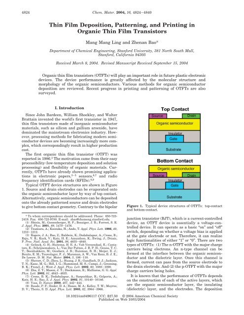
Typical OTFT device structures are shown <strong>in</strong> Figure<br />
1. Source <strong>and</strong> dra<strong>in</strong> electrodes can be evaporated onto<br />
the organic semiconductor layer by way of top contact.<br />
Alternatively, organic semiconductors can be deposited<br />
onto the already patterned source <strong>and</strong> dra<strong>in</strong> electrodes<br />
to give bottom contact geometry. Contrary to the bipolar<br />
* To whom correspondence should be addressed. Phone: 650-723-<br />
2419. Fax: 650-723-9780. E-mail: zbao@chemeng.stanford.edu.<br />
(1) Shte<strong>in</strong>, M.; Gossenberger, H. F.; Benziger, J. B.; Forrest, S. R.<br />
J. Appl. Phys. 2001, 89, 1470-1476.<br />
(2) Tsumura, A.; Koezuka, H.; Ando, T. Appl. Phys. Lett. 1986, 49,<br />
1210-1212.<br />
(3) Rogers, J. A.; Bao, Z.; Baldw<strong>in</strong>, K.; Dodabalapur, A.; Crone, B.;<br />
Raju, V. R.; Kuck, V.; Katz, H. E.; Amundson, K.; Ew<strong>in</strong>g, J.; Drzaic,<br />
P. Proc. Natl. Acad. Sci. 2001, 98, 4835-4840.<br />
(4) Gel<strong>in</strong>ck, G. H.; Huitema, H. E. A.; Vab Veenendaal, E.; Cantatore,<br />
E.; Schrijnemakers, L.; Van Der Putten, J. B. P. H.; Geuns, T. C.<br />
T.; Beenhakkers, M.; Giesbers, J. B.; Huisman, B. H.; Meijer, E. J.;<br />
Benito, E. M.; Touwslager, F. J.; Marsman, A. W.; Van Rens, B. J. E.;<br />
De Leeuw, D. M. Nat. Mater. 2004, 3, 106-110.<br />
(5) Sheraw, C. D.; Zhou, L.; Huang, J. R.; Gundlach, D. J.; Jackson,<br />
T. N.; Kane, M. G.; Hill, I. G.; Hammond, M. S.; Campi, J.; Green<strong>in</strong>g,<br />
B. K.; Francl, J.; West J. Appl. Phys. Lett. 2002, 80, 1088-1090.<br />
(6) Zhu, Z. T.; Mason, J. T.; Dieckmann, R.; Malliaras, G. G. Appl.<br />
Phys. Lett. 2002, 81, 4643-4635.<br />
(7) Crone, B. K.; Dodabalapur, A.; Sarpeshkar, R.; Gelper<strong>in</strong>, A.;<br />
Katz, H. E.; Bao, Z. J. Appl. Phys. 2002, 91, 10140-10146.<br />
(8) Voss, D. Nature 2000, 407, 442-444.<br />
(9) Baude, P. F.; Ender, D. A.; Haase, M. A.; Kelley, T. W.; Muyres,<br />
D. V.; Thesis, S. D. Appl. Phys. Lett. 2003, 82, 3964-3966.<br />
Figure 1. Typical device structures of OTFTs: top-contact<br />
<strong>and</strong> bottom-contact.<br />
junction transistor (BJT), which is a current-controlled<br />
device, an OTFT device is essentially a voltage-controlled<br />
device. It can operate as a basic “on” <strong>and</strong> “off”<br />
switch, depend<strong>in</strong>g on whether a voltage bias is applied<br />
at the gate electrode or not. Therefore, it can realize<br />
logic functionalities of either “1” or “0”. There are two<br />
types of OTFTs: (1) The n-OTFT with the major charge<br />
carriers be<strong>in</strong>g electrons. An n-type channel can be<br />
formed at the <strong>in</strong>terface between the organic semiconductor<br />
<strong>and</strong> the dielectric layer. Once this channel is<br />
formed, current can pass from the source electrode to<br />
the dra<strong>in</strong> electrode. And (2) the p-OTFT with the major<br />
charge carriers be<strong>in</strong>g holes.<br />
It is known that the performance of OTFTs depends<br />
on the construction of each of the active layers, which<br />
are the organic semiconductor layer, the <strong>in</strong>sulat<strong>in</strong>g<br />
(dielectric) layer, <strong>and</strong> the electrodes. The deposition<br />
10.1021/cm0496117 CCC: $27.50 © 2004 American Chemical Society<br />
Published on Web 10/01/2004
<strong>Organic</strong> <strong>Th<strong>in</strong></strong> <strong>Film</strong> Transistors Chem. Mater., Vol. 16, No. 23, 2004 4825<br />
method, condition, sequence, postdeposition treatment,<br />
<strong>and</strong> surface treatment significantly impact OTFT performance.<br />
Therefore, it is important to fully underst<strong>and</strong><br />
various factors that affect the th<strong>in</strong> film growth processes.<br />
Specifically, one needs to pay attention to how<br />
the molecular structure of the organic semiconductor<br />
<strong>and</strong> th<strong>in</strong> film morphology affect the performance of<br />
OTFT devices, namely, the field effect mobility <strong>and</strong> on/<br />
off ratio.<br />
This review <strong>in</strong>tends to summarize recent progress on<br />
methods for th<strong>in</strong> film deposition <strong>and</strong> pattern formation<br />
for OTFTs. Follow<strong>in</strong>g an <strong>in</strong>troduction <strong>in</strong> section I,<br />
methods for organic semiconductor th<strong>in</strong> film deposition<br />
are presented <strong>in</strong> section II. The effects of the surface<br />
chemical functionalities <strong>and</strong> surface treatment on the<br />
organic semiconductor th<strong>in</strong> film growth will be discussed<br />
<strong>in</strong> section III. Methods for pattern<strong>in</strong>g <strong>and</strong> pr<strong>in</strong>t<strong>in</strong>g are<br />
surveyed <strong>in</strong> section IV. F<strong>in</strong>ally, a summary <strong>in</strong> section<br />
V will conclude this review.<br />
II. Semiconductor <strong>Deposition</strong> Methods<br />
In this section, various semiconductor deposition<br />
methods are discussed. In general, organic semiconductors<br />
are deposited either from vapor or solution phase<br />
depend<strong>in</strong>g on their vapor pressure <strong>and</strong> solubility. As<br />
mentioned earlier, device performance is greatly <strong>in</strong>fluenced<br />
by various deposition conditions due to the<br />
different result<strong>in</strong>g molecular structure <strong>and</strong> th<strong>in</strong> film<br />
morphology. <strong>Organic</strong> materials tend to pack <strong>in</strong>to either<br />
a herr<strong>in</strong>gbone (for example, R-6T 10 )oraπ-π stack<strong>in</strong>g<br />
structure (for example, bis(benzodithiophene) 11 ), governed<br />
by <strong>in</strong>termolecular <strong>in</strong>teractions. Better overlap<br />
between the π molecular orbitals generally results <strong>in</strong> a<br />
higher mobility, as suggested by quantum chemical<br />
calculations. 12 To achieve high field effect mobility, the<br />
semiconduct<strong>in</strong>g molecules should have an orientation<br />
<strong>in</strong> which the π-π stack<strong>in</strong>g direction between molecules<br />
is arranged <strong>in</strong> the same direction as that of the current<br />
flow. Moreover, larger gra<strong>in</strong> sizes <strong>and</strong> smooth gra<strong>in</strong>s<br />
usually tend to give better mobilities. 13 It is known that<br />
the current flow <strong>in</strong> an organic field-effect transistor<br />
(OFET) is ma<strong>in</strong>ly conf<strong>in</strong>ed <strong>in</strong> the first 50 Å of semiconductor<br />
layer away from the semiconductor/dielectric<br />
<strong>in</strong>terface. 14 The typical semiconductor thickness required<br />
for an OFET is <strong>in</strong> the range of 200-500 Å. A<br />
th<strong>in</strong>ner film may have <strong>in</strong>complete surface coverage. For<br />
bottom-contact devices, a thicker semiconductor layer<br />
usually does not affect the charge carrier mobility even<br />
though the device off-current may <strong>in</strong>crease for materials<br />
with a higher un<strong>in</strong>tentional dop<strong>in</strong>g. For top-contact<br />
devices, a thicker layer may lead to higher resistance<br />
for the charge carriers to travel from the source electrode<br />
to the semiconductor/dielectric <strong>in</strong>terface, where<br />
the majority of the current flow occurs.<br />
(10) Siegrist, T.; Flem<strong>in</strong>g, R. M.; Haddon, R. C.; Laudise, R. A.;<br />
Lov<strong>in</strong>ger, A. J.; Katz, H. E.; Bridenbaugh, P.; Davis, D. D. J. Mater.<br />
Res. 1995, 10, 2170-2174.<br />
(11) Li, X. C.; Sirr<strong>in</strong>ghaus, H.; Garnier, F.; Holmes, A. B.; Moratti,<br />
S. C.; Feeder, N.; Clegg, W.; Teat, S. J.; Friend, R. H. J. Am. Chem.<br />
Soc. 1998, 120, 2206-2207.<br />
(12) Cornil, J.; Beljonne, D.; Calbert, J. P.; Bredas, J. L. Adv. Mater.<br />
2001, 13, 1053-1067.<br />
(13) Bao, Z.; Lov<strong>in</strong>ger, A. J.; Dodabalapour, A. Adv. Mater. 1997,<br />
9, 42-44.<br />
(14) Alam, M. A.; Dodabalapur, A.; P<strong>in</strong>to, M. R. IEEE Trans.<br />
Electron Devices 1997, 44, 1332-1337.<br />
Figure 2. Schematic diagram of OVPD. Repr<strong>in</strong>ted with<br />
permission from ref 1. Copyright 2001 American Institute of<br />
Physics.<br />
1. Vacuum <strong>Deposition</strong>. Vacuum thermal evaporation<br />
<strong>in</strong>volves heat<strong>in</strong>g the organic semiconductor us<strong>in</strong>g<br />
a resistive heat<strong>in</strong>g source under a vacuum environment<br />
with a pressure <strong>in</strong> the range of 10 -8 to 10 -6 Torr. For<br />
organic small molecules <strong>and</strong> oligomers that are solution<strong>in</strong>soluble,<br />
vacuum thermal evaporation is an ideal<br />
deposition method. A number of organic semiconductors<br />
have been deposited us<strong>in</strong>g this method. Examples are<br />
oligothiophene <strong>and</strong> oligofluorene derivatives, 15-17 metallophthalocyan<strong>in</strong>es,<br />
13,18 <strong>and</strong> acenes (pentacene <strong>and</strong><br />
tetracene). 19-25 Currently, the best mobility for organic<br />
semiconductors has been reported for vacuum-deposited<br />
pentacene films. 19,20,23 Vacuum thermal evaporation has<br />
the advantages of form<strong>in</strong>g films with high film uniformity<br />
<strong>and</strong> good “run-to-run” reproducibility. Multilayer<br />
deposition <strong>and</strong> co-deposition of several organic<br />
semiconductors are possible without the concerns of<br />
delam<strong>in</strong>ation or dissolution of the previous layers dur<strong>in</strong>g<br />
subsequent deposition steps. However, this method has<br />
a relatively high material consumption <strong>and</strong> also a high<br />
<strong>in</strong>itial cost for equipment setup. Nevertheless, this<br />
method has already been used for the manufactur<strong>in</strong>g<br />
of organic small molecule based light emitt<strong>in</strong>g displays<br />
by several companies.<br />
Other vacuum based th<strong>in</strong> film deposition methods<br />
employed for OFET fabrication <strong>in</strong>clude: organic vapor<br />
phase deposition (OVPD), organic molecular beam<br />
deposition (OMBD), <strong>and</strong> laser evaporation. <strong>Organic</strong><br />
vapor phase deposition (Figure 2) proceeds by evaporation<br />
of the molecular source material <strong>in</strong>to a stream of<br />
hot <strong>in</strong>ert carrier gas such as nitrogen or argon, which<br />
then transports the vapor toward a cooled substrate<br />
(15) Mushrush, M.; Facchetti, A.; Lefenfeld, M.; Katz, H. E.; Marks,<br />
T. J. J. Am. Chem. Soc. 2003, 125, 9414-9423.<br />
(16) Garnier, F.; Hailaoui, R.; Yassar, A.; Srivastava, P. 1994.<br />
(17) Katz, H. E.; Bao, Z.; Gilat, S. L. Acc. Chem. Res. 2001, 34, 359-<br />
369.<br />
(18) Bao, Z.; Lov<strong>in</strong>ger, A. J.; Dodabalapour, A. Appl. Phys. Lett.<br />
1996, 69, 3066-3068.<br />
(19) Kelly, T. W.; Boardman, L. D.; Dunbar, T. D.; Muyres, D. V.;<br />
Pellerite, M. J.; Smith, T. P. J. Phys. Chem. B 2003, 107, 5877-<br />
5881.<br />
(20) Klauk, H.; Gundlach, D. J.; Nichols, J. A.; Sheraw, C. D.; Bonse,<br />
M.; Jackson, T. N. Solid State Technol. 2000, 43, 63-77.<br />
(21) Anthony, J. E.; Brooks, J. S.; Eaton, D. L.; Park<strong>in</strong>, S. R. J.<br />
Am. Chem. Soc. 2001, 123, 9482-9483.<br />
(22) Gundlach, D. J.; Nichols, J. A.; Zhou, L.; Jackson, T. N. Appl.<br />
Phys. Lett. 2002, 80, 2925-2927.<br />
(23) Klauk, H.; Halik, M.; Zschieschang, U.; Eder, F.; Schmid, G.;<br />
Dehm, C. Appl. Phys. Lett. 2003, 82, 4175-4177.<br />
(24) Chang, J.-W.; Kim, H.; Kim, J.-K.; Ju, B. K. J. Korean Phys.<br />
Soc. 2003, 42, S268-S272.<br />
(25) K<strong>in</strong>ipp, D.; Street, R. A.; Volkel, A. R. Appl. Phys. Lett. 2003,<br />
82, 3907-3909.
4826 Chem. Mater., Vol. 16, No. 23, 2004 L<strong>in</strong>g <strong>and</strong> Bao<br />
where condensation of the organics occurs. 1,26 With<br />
typical conditions used, the flow of the carrier gas<br />
around the substrate creates a hydrodynamic boundary<br />
layer where molecular transport is diffusion limited. The<br />
deposition rate, deposition efficiency, <strong>and</strong> film morphology<br />
are controlled by adjust<strong>in</strong>g the organic species<br />
concentration, flow hydrodynamics, <strong>and</strong> surface diffusivity.<br />
26,27 S<strong>in</strong>ce the flow patterns may be eng<strong>in</strong>eered,<br />
the advantages of this approach <strong>in</strong>clude substrateselective<br />
deposition <strong>and</strong> uniform distribution of organic<br />
vapors result<strong>in</strong>g <strong>in</strong> a very uniform coat<strong>in</strong>g thickness<br />
with m<strong>in</strong>imized waste of materials. It has been used to<br />
prepare multiplayer organic light-emitt<strong>in</strong>g diode (OLED)<br />
devices. 28-30 Recently, pentacene films have been prepared<br />
us<strong>in</strong>g OVPD <strong>and</strong> their transistor performance<br />
hase been <strong>in</strong>vestigated. 27 Performance similar to films<br />
prepared by vacuum thermal evaporation was obta<strong>in</strong>ed.<br />
Evaporation of organic materials <strong>in</strong> an ultrahigh<br />
vacuum (UHV) is sometimes referred to as organic<br />
molecular beam deposition (OMBD) or organic molecular<br />
beam epitaxy (OMBE). 31 Monolayer control over<br />
the growth of organic th<strong>in</strong> films with extremely high<br />
chemical purity <strong>and</strong> structural precision is possible with<br />
this deposition method. This method can be comb<strong>in</strong>ed<br />
with <strong>in</strong> situ high-resolution structural diagnostic tools<br />
as the films are be<strong>in</strong>g deposited <strong>and</strong> allows for underst<strong>and</strong><strong>in</strong>g<br />
of the fundamental structural <strong>and</strong> optoelectronic<br />
properties of ultrath<strong>in</strong> organic film systems. It<br />
has been used for deposition of pentacene OFETs, <strong>and</strong><br />
was observed to give a mobility of 0.038 cm 2 /Vs. 32 This<br />
lower mobility compared to those obta<strong>in</strong>ed with typical<br />
vacuum thermal evaporation may be related to the<br />
formation of two pentacene phases at a relatively low<br />
evaporation rate typical for OMBD. 32 Gross et al. have<br />
successfully grown perylene monolayer on Au(110) us<strong>in</strong>g<br />
OMBE. 33 Recently, a modified OMBD for organic semiconductors,<br />
namely seeded supersonic molecular beam<br />
epitaxy (SuMBE) technique 34,35 was reported by S.<br />
Iannotta et al. The vapor of the resistively heated raw<br />
material was “seeded” <strong>in</strong> a He carrier gas flow<strong>in</strong>g <strong>in</strong>to<br />
a capillary. The molecular precursors <strong>in</strong> the beams are<br />
highly regulated <strong>in</strong> terms of k<strong>in</strong>etic energy at the <strong>in</strong>itial<br />
state of deposition. This method thus allows good control<br />
of the th<strong>in</strong> film morphology, structure, <strong>and</strong> functional<br />
properties of the result<strong>in</strong>g films. Oligothiophenes, pentacene,<br />
<strong>and</strong> phthalocyan<strong>in</strong>e films have been deposited<br />
by this method. 34,35 <strong>Film</strong>s with high crystall<strong>in</strong>ity were<br />
formed attributed to the local anneal<strong>in</strong>g <strong>in</strong>duced by the<br />
<strong>in</strong>itial k<strong>in</strong>etic energy of the molecules <strong>in</strong> the supersonic<br />
(26) Shte<strong>in</strong>, M.; Peumans, P.; Benziger, J. B.; Forrest, S. R. J. Appl.<br />
Phys. 2003, 93, 4005-4016.<br />
(27) Shte<strong>in</strong>, M.; Mapel, J.; Benziger, J. B.; Forrest, S. R. Appl. Phys.<br />
Lett. 2002, 81, 268-270.<br />
(28) Burrows, P. E.; Forrest, S. R.; Sapochak, L. S.; Schwartz, J.;<br />
Fenter, P.; Buma, T.; Ban, V. S.; Forrest, J. L. J. Cryst. Growth 1995,<br />
156, 91-95.<br />
(29) Vaeth, K. M.; Jensen, K. Appl. Phys. Lett. 1997, 71, 2091-<br />
2093.<br />
(30) Baldo, M. A.; Kozlov, V. G.; Burrows, P. E.; Forrest, S. R.; Ban,<br />
V. S.; Koene, B.; Thompson, M. E. Appl. Phys. Lett. 1997, 71, 3033-<br />
3035.<br />
(31) Forrest, S. R. Chem. Rev. 1997, 97, 1793-1896.<br />
(32) Dimitrakopoulos, C. D.; Brown, A. R.; Pomp, A. J. Appl. Phys.<br />
1996, 80, 2501-2508.<br />
(33) Gross, L.; Seidel, C.; Fuchs, H. Org. Electron. 2002, 3, 1-7.<br />
(34) Iannotta, S.; Toccoli, T. J. Polym. Sci., Part B: Polym. Phys.<br />
2003, 41, 2501-2521.<br />
(35) Iannotta, S.; Toccoli, T.; Biasioli, F.; Boschetti, A.; Ferrari, M.<br />
Appl. Phys. Lett. 2000, 76, 1845-1847.<br />
beam. However, no OFET performance based on films<br />
deposited by this method has been reported.<br />
Laser ablation technique, which is widely used for<br />
deposition of a variety of <strong>in</strong>organic materials, has also<br />
been applied to the deposition of organic semiconductors.<br />
A pulsed ultraviolet laser is used to <strong>in</strong>duce<br />
evaporation as comparable to those produced via thermal<br />
evaporation. 36 The vaporized organic semiconductor<br />
condenses on a nearby cooled substrate. It was found<br />
that laser-deposited pentacene films had properties<br />
(such as optical properties, field effect mobilities, <strong>and</strong><br />
surface morphology) similar to those of the thermally<br />
evaporated films. 36 Pentacene films produced this way<br />
conta<strong>in</strong> a s<strong>in</strong>gle-phase with <strong>in</strong>terlamella spac<strong>in</strong>g characteristic<br />
of the th<strong>in</strong>-film phase. 36 This technique has<br />
also been used for the deposition of other materials such<br />
as poly(ethylene-alt-maleic anhydride). 37<br />
Several factors should be considered when select<strong>in</strong>g<br />
the deposition conditions <strong>in</strong> order to achieve high OTFT<br />
performance. First, deposition rate <strong>and</strong> substrate temperature<br />
directly affect the crystall<strong>in</strong>ity <strong>and</strong> morphology<br />
of the result<strong>in</strong>g th<strong>in</strong> film. Second, the substrate surface<br />
onto which the organic semiconductor materials are<br />
deposited also has a great impact on the formation of<br />
the th<strong>in</strong> film, <strong>and</strong> thus the performance of the result<strong>in</strong>g<br />
device. F<strong>in</strong>ally, postdeposition treatments, such as<br />
anneal<strong>in</strong>g, may further improve device performance <strong>and</strong><br />
characteristics. Even though different vapor phase<br />
deposition methods may be used, many of the considerations<br />
for deposition conditions, surface treatment,<br />
<strong>and</strong> postdeposition anneal<strong>in</strong>g are similar. They will be<br />
discussed <strong>in</strong> greater detail later <strong>in</strong> the follow<strong>in</strong>g sections.<br />
2. Solution <strong>Deposition</strong>. <strong>Deposition</strong> methods based<br />
on solution-processable materials are not limited by the<br />
size of the vacuum chamber <strong>and</strong> no pump<strong>in</strong>g down time<br />
is required. They are compatible with large-area th<strong>in</strong><br />
film fabrication <strong>and</strong> therefore result <strong>in</strong> lower production<br />
cost per device. Solution deposition, such as screen<br />
pr<strong>in</strong>t<strong>in</strong>g <strong>and</strong> <strong>in</strong>k jet pr<strong>in</strong>t<strong>in</strong>g, 38-43 also allows the<br />
possibility of pr<strong>in</strong>t<strong>in</strong>g the active materials <strong>in</strong> which the<br />
deposition <strong>and</strong> pattern<strong>in</strong>g are accomplished <strong>in</strong> a s<strong>in</strong>gle<br />
step. 44 Two approaches have been used to obta<strong>in</strong> organic<br />
semiconductor th<strong>in</strong> films from solution: (1) deposition<br />
of a soluble precursor from solution <strong>and</strong> subsequent<br />
conversion <strong>in</strong>to the f<strong>in</strong>al semiconductor; or (2) direct<br />
deposition of a soluble semiconductor.<br />
Most conjugated oligomers <strong>and</strong> polymers used as<br />
semiconductors are <strong>in</strong>soluble <strong>in</strong> common solvents unless<br />
solubiliz<strong>in</strong>g substitutions are <strong>in</strong>corporated <strong>in</strong>to the<br />
(36) Blanchet, G. B.; F<strong>in</strong>cher, C. R.; Malajovich, I. J. Appl. Phys.<br />
2003, 94, 6181-6184.<br />
(37) Pola, J.; Kupcik, J.; Durani, S. M. A.; Khavaja, E. E.; Masoudi,<br />
H. M.; Bastl, Z.; Subrt, J. Chem. Mater. 2003, 15, 3887-3893.<br />
(38) Jabbour, G. E.; Radsp<strong>in</strong>ner, R.; Peyghambarian, N. IEEE J.<br />
Sel. Top. Quantum Electron. 2001, 7, 769-773.<br />
(39) Bao, Z.; Feng, Y.; Dodabalapur, A.; Raju, V. R.; Lov<strong>in</strong>ger, A. J.<br />
Chem. Mater. 1997, 9, 1299-1301.<br />
(40) Sirr<strong>in</strong>ghaus, H.; Kawase, T.; Friend, R. H.; Shimoda, T.;<br />
Inbasekaran, M.; Wu, W.; Woo, E. P. Science 2000, 290, 2123-2126.<br />
(41) Kawase, T.; Sirr<strong>in</strong>ghaus, H.; Friend, R. H.; Shimoda, T. Adv.<br />
Mater. 2001, 13, 1601-1605.<br />
(42) Aernouts, T.; Vanlaeke, P.; Geens, W.; Poortmans, J.; Heremans,<br />
P.; Borghs, S.; Mertens, R.; Andriessen, R.; Leenders, L. <strong>Th<strong>in</strong></strong><br />
Solid <strong>Film</strong>s 2004, 451, 22-25.<br />
(43) M<strong>in</strong>, G. Synth. Met. 2003, 135, 141-143.<br />
(44) Bao, Z.; Rogers, J. A.; Katz, H. E. J. Mater. Chem. 1999, 9,<br />
1895-1904.
<strong>Organic</strong> <strong>Th<strong>in</strong></strong> <strong>Film</strong> Transistors Chem. Mater., Vol. 16, No. 23, 2004 4827<br />
Scheme 1. Conversion Reaction from a Precursor<br />
Polymer to Poly(2,5-thienylenev<strong>in</strong>ylene) (PTV)<br />
(Repr<strong>in</strong>ted with permission from ref 49; Copyright<br />
1993 American Institute of Physics)<br />
molecular structures. Sometimes, these substitutions<br />
may either <strong>in</strong>terfere with molecular pack<strong>in</strong>g or <strong>in</strong>crease<br />
the π-π stack<strong>in</strong>g distance between molecules, both of<br />
which result <strong>in</strong> lower charge carrier mobilities. Electrochemical<br />
polymerization has been used to synthesize<br />
<strong>and</strong> deposit polythiophene semiconductor directly <strong>in</strong>to<br />
the channel region. 2 However, polymers prepared this<br />
way tend to be partially doped <strong>and</strong> usually have low<br />
on/off ratios. In addition, the field-effect mobility of this<br />
polymer is low because it is partially cross-l<strong>in</strong>ked dur<strong>in</strong>g<br />
the polymerization process <strong>and</strong> results <strong>in</strong> poor molecular<br />
order<strong>in</strong>g. To overcome these problems, several groups<br />
have taken the approach of synthesiz<strong>in</strong>g soluble precursors<br />
which can subsequently be converted <strong>in</strong>to the f<strong>in</strong>al<br />
semiconductor after film deposition from solution. Pentacene<br />
transistors with high mobilities have been reported<br />
us<strong>in</strong>g this approach. 45-47 Oligothiophene <strong>and</strong><br />
poly(thienylene v<strong>in</strong>ylene) transistors have also been<br />
prepared with reasonable mobilities. 48-50 Another <strong>in</strong>terest<strong>in</strong>g<br />
example <strong>in</strong>volves deposition of an n-channel<br />
ladder polymer from solution us<strong>in</strong>g a Lewis acid act<strong>in</strong>g<br />
both as a chelat<strong>in</strong>g <strong>and</strong> solubiliz<strong>in</strong>g group. After film<br />
deposition, the Lewis acid was removed by extensive<br />
wash<strong>in</strong>g. 51,52 High n-channel mobility was reported with<br />
the proper selection of Lewis acid, which results <strong>in</strong> th<strong>in</strong><br />
films of highly ordered polymers. 52 However, the catalyst<br />
has to be completely removed, otherwise undesired<br />
mobile ions may be present <strong>in</strong> the film <strong>and</strong> lead to<br />
unusual electrical characteristics. 51 As an illustration,<br />
the conversion reaction from a precursor polymer to<br />
poly(2,5-thienylenev<strong>in</strong>ylene) (PTV) at 200 °C is shown<br />
<strong>in</strong> Scheme 1. 49<br />
The conversion temperature for precursor materials<br />
required for achiev<strong>in</strong>g high mobility tends to be high<br />
(above 125 °C) <strong>and</strong> may be <strong>in</strong>compatible with low-cost<br />
plastic substrates. The additional conversion step is also<br />
time-consum<strong>in</strong>g. Therefore, direct deposition of soluble<br />
semiconductor is more desirable. Both polymers <strong>and</strong><br />
oligomers have been directly deposited from solution.<br />
Polymers tend to have better th<strong>in</strong> film form<strong>in</strong>g properties<br />
with good uniformity over a large area. However,<br />
they are more difficult to purify <strong>and</strong> it is harder to<br />
achieve good long-range molecular order<strong>in</strong>g. The best<br />
(45) Herwig, P. T.; Mullen, K. Adv. Mater. 1999, 11, 480-483.<br />
(46) Afzali, A.; Dimitrakopoulos, C. D.; Breen, T. L. J. Am. Chem.<br />
Soc. 2002, 124, 8812-8813.<br />
(47) Afzali, A.; Dimitrakopoulos, C. D.; Graham, T. O. Adv. Mater.<br />
2003, 15, 2066-2069.<br />
(48) Murphy, A. R.; Frechet, J. M. J.; Chang, P.; Lee, J.; Subramanian,<br />
V. J. Am. Chem. Soc. 2004, 126, 1596-1597.<br />
(49) Fuchigami, H.; Tsumura, A.; Koezuka, H. Appl. Phys. Lett.<br />
1993, 63, 1372-1374.<br />
(50) Brown, A. R.; Pomp, A.; Hart, C. M.; De Leeuw, D. M. Science<br />
1995, 270, 972-974.<br />
(51) Chen, X. L.; Bao, Z.; Lov<strong>in</strong>ger, A. J.; L<strong>in</strong>, Y. Y.; Crone, B.;<br />
Dodabalapur, A.; Batlogg, B. Appl. Phys. Lett. 2001, 78, 228-230.<br />
(52) Babel, A.; Jenekhe, S. A. J. Am. Chem. Soc. 2003, 125, 13656-<br />
13657.<br />
mobility, <strong>in</strong> the order of 0.1 cm 2 /Vs, is obta<strong>in</strong>ed with<br />
solution-deposited polymer such as regioregular poly-<br />
(3-hexylthiophene) (PHT) <strong>and</strong> a structurally modified<br />
derivative. 18,53-56 Much work has been done to study<br />
PHT TFTs. 57-61 Oligomers, on the other h<strong>and</strong>, can be<br />
easily purified by column or sublimation. However, they<br />
tend to be highly crystall<strong>in</strong>e <strong>and</strong> thus it is difficult to<br />
form a smooth uniform film over a large area. High<br />
mobilities have been reported with several oligomers by<br />
optimiz<strong>in</strong>g the deposition conditions. 62-64<br />
Both sp<strong>in</strong>-coat<strong>in</strong>g <strong>and</strong> solution-cast<strong>in</strong>g are commonly<br />
used for solution deposition. 61,65-68 In the sp<strong>in</strong>-coat<strong>in</strong>g<br />
method, the solvent dries relatively fast allow<strong>in</strong>g less<br />
time for molecular order<strong>in</strong>g compared to that <strong>in</strong> solution-cast<strong>in</strong>g.<br />
But the film uniformity is usually better<br />
for sp<strong>in</strong>-coated films. These films can be annealed<br />
afterward to improve molecular order<strong>in</strong>g as discussed<br />
later. For materials with tendencies to form highly<br />
ordered molecular pack<strong>in</strong>g, it was found that even sp<strong>in</strong>coated<br />
films can achieve very high mobilities. 53 For<br />
example, for regioregular poly(3-hexylthiophene) with<br />
80% regioregularity, the plane of the thiophene r<strong>in</strong>gs<br />
<strong>in</strong> the polymer backbone are primarily oriented parallel<br />
to the substrate surface (Figure 3b) <strong>in</strong> the sp<strong>in</strong>-coated<br />
film, while the solution-cast film has the thiophene r<strong>in</strong>gs<br />
perpendicular to the substrate surface (Figure 3a)<br />
result<strong>in</strong>g <strong>in</strong> an <strong>in</strong>crease of mobility by more than 1 order<br />
of magnitude. 53 If the regioregularity was greater than<br />
95%, similar mobilities were obta<strong>in</strong>ed with both sp<strong>in</strong>coated<br />
<strong>and</strong> solution-cast films. 53<br />
For solution deposition, semiconductor concentration,<br />
solvent evaporation rate, solubility of the semiconductor,<br />
<strong>and</strong> the nature of the substrate surface play important<br />
roles <strong>in</strong> the quality of the result<strong>in</strong>g semiconductor films.<br />
The solvent dependence of highly regioregular (>95%)<br />
poly(3-hexylthiophene) has been studied. 18,69 It was<br />
found that the mobilities of these polymer transistors<br />
(53) Sirr<strong>in</strong>ghaus, H.; Brown, P. J.; Friend, R. H.; Nielsen, M. M.;<br />
Bechgaard, K.; Langeveld, V., B. M. W.; Spier<strong>in</strong>g, A. J. H.; Janssen,<br />
R. A. J.; Meijer, E. W.; Herwig, P.; de Leeuw, D. M. Nature 1999, 401,<br />
685-688.<br />
(54) Ong, B.; Wu, Y. L.; Liu, P.; Gardner, S. J. Am. Chem. Soc. 2004,<br />
126, 3378-3379.<br />
(55) Ong, B.; Wu, Y. L.; Jiang, L.; P. L.; Muck, T. Synth. Met. 2004,<br />
142, 49-52.<br />
(56) Kim, Y. H.; Park, S. K.; Moon, D. G.; Kim, W. K.; Han, J. I.<br />
Jpn. J. Appl. Phys. 2004, 43, 3605-3608.<br />
(57) Hosh<strong>in</strong>o, S. Y. M.; Uemura, S.; Kodzasa, T.; Takada, N.;<br />
Kamata, T.; Yase, K. J. Appl. Phys. 2004, 95, 5088-5093.<br />
(58) Wang, G. M.; Moses, D.; Heeger, A. J.; Zhang, H. M.; Narasimhan,<br />
M.; Demaray, R. E. J. Appl. Phys. 2004, 95, 316-322.<br />
(59) Yang, Y. S.; Kim, S. H.; Lim, S. C.; Lee, J. I.; Lee, J. H.; Do, L.<br />
M.; Zyung, T. Appl. Phys. Lett. 2003, 83, 3939-3941.<br />
(60) Burgi, L.; Richards, T. J.; Friend, R. H.; Sirr<strong>in</strong>ghaus, H. J. Appl.<br />
Phys. 2003, 94, 6129-6137.<br />
(61) Yang, H. C.; Sh<strong>in</strong>, T. J.; Yang, L.; Cho, K.; Chang, Y. R.; Bao,<br />
Z. Adv. Func. Mater. 2004.<br />
(62) Garnier, F.; Hajlaoui, R.; El Kassmi, M. Appl. Phys. Lett. 1998,<br />
73, 1721-1723.<br />
(63) Lefenfeld, M.; Gopalan, P.; Mushrush, M.; Ocko, B.; Gang, O.;<br />
Jisrawi, N.; Siegrist, T.; Katz, H. E. J. Phys. Chem. B 2004.<br />
(64) Sheraw, C. D.; Jackson, T. N.; Eaton, D. L.; Anthony, J. E.<br />
Adv. Mater. 2003, 15, 2009-2011.<br />
(65) Park, S. K.; Kim, Y. H.; Han, J. I.; Moon, D. G.; Kim, W. K.;<br />
Kwak, M. G. Synth. Met. 2003, 139, 377-384.<br />
(66) Michaelis, W.; Kelt<strong>in</strong>g, C.; Hirth, A.; Wohrle, D.; Schlettwe<strong>in</strong>,<br />
D. Macromol. Symp. 2004, 212, 299-305.<br />
(67) Cui, T. H.; Liang, G. R.; Varahramyan, K. IEEE Trans. Electron<br />
Devices 2003, 50, 1419-1422.<br />
(68) Liang, G. R.; Cui, T. H.; Varahramyan, K. Microelectron. Eng.<br />
2003, 65, 279-284.<br />
(69) Yang, H.; Sh<strong>in</strong>, T. J.; Yang, L.; Bao, Z.; Ryu, C. Y.; Siegel, R.<br />
W.; Cho, K. Polym. Prepr. 2004, 45, 212-213.
4828 Chem. Mater., Vol. 16, No. 23, 2004 L<strong>in</strong>g <strong>and</strong> Bao<br />
Figure 3. Two different orientations of ordered P3HT doma<strong>in</strong>s with respect to the FET substrate. (a <strong>and</strong> b) The wide-angle<br />
X-ray scatter<strong>in</strong>g images are a color representation of the two-dimensional distribution of scattered Cu KR X-ray <strong>in</strong>tensity from<br />
sp<strong>in</strong>-coated, 70-100-nm-thick P3HT films with regioregularity of 96% (a) <strong>and</strong> 81% (b) on SiO2/Si substrates. (c) Dependence of<br />
the room-temperature mobility on the regioregularity for sp<strong>in</strong>-coated (downward triangles) <strong>and</strong> solution-cast (upward triangles)<br />
top-contact P3HT FETs (channel length L ) 75 µm, channel width W ) 1.5 mm). Repr<strong>in</strong>ted with permission from ref 53. Copyright<br />
1999 Nature Publish<strong>in</strong>g Group.<br />
are highly dependent on the solvent used for cast<strong>in</strong>g<br />
films. The best solvent was chloroform, which gives films<br />
with densely packed <strong>and</strong> <strong>in</strong>terconnected nanofibrils<br />
morphology. 69 The structure analysis with graz<strong>in</strong>g<br />
<strong>in</strong>cidence wide-angle X-ray diffraction (GIWAX) <strong>in</strong>dicated<br />
that the polymer conformations are similar regardless<br />
of the solvent used for film preparation, i.e.,<br />
similar polymer orientation as shown <strong>in</strong> Figure 3a was<br />
found for PHT with more than 95% regioregularity. The<br />
difference <strong>in</strong> mobility was thus attributed to the difference<br />
<strong>in</strong> the nanofibrils morphology. When the fibrils are<br />
densely packed <strong>in</strong> the case of chloroform as a solvent,<br />
the th<strong>in</strong> film mobility is higher than that of the loosely<br />
packed fibrils that result when methylene chloride is<br />
used as the solvent. 69<br />
For polymer semiconductors, their molecular weight<br />
<strong>and</strong> polydispersity also have great impact on the<br />
morphology of their th<strong>in</strong> films. Recent work has shown<br />
that the mobility of sp<strong>in</strong>-coated regioregular poly(3hexylthiophene)<br />
differs by several orders of magnitudes<br />
depend<strong>in</strong>g on the molecular weight of the polymer. 70 The<br />
mobility was found to <strong>in</strong>crease with molecular weight.<br />
Low-molecular-weight PHTs (number-averaged molecular<br />
weight less than 10 000) were found to form rodlike<br />
morphology, whereas high-molecular-weight polymers<br />
formed isotropic nodules. It is unclear whether the<br />
difference <strong>in</strong> mobility is due to the sharper <strong>in</strong>terface<br />
between rods <strong>in</strong> the low-molecular-weight films or the<br />
fact that the larger-sized molecules require less hopp<strong>in</strong>g<br />
between molecules. 70<br />
The Langmuir-Blodgett (LB) technique is another<br />
possible method to deposit organic semiconductor th<strong>in</strong><br />
films. 71-75 LB film is an ordered array of amphiphillic<br />
molecules formed by compression with a blade on a<br />
water surface. The film can then be transferred onto a<br />
(70) Kl<strong>in</strong>e, J. R.; McGehee, M. D. Adv. Mater. 2003, 15, 1519-1522.<br />
(71) Paloheimo, J.; Kuivala<strong>in</strong>en, P.; Stubb, H.; Vuorimaa, E.; Yli-<br />
Lahti, P. Appl. Phys. Lett. 1990, 56, 1157-1159.<br />
(72) Xu, G. F.; Bao, Z.; Groves, J. T. Langmuir 2000, 16, 1834-<br />
1841.<br />
(73) Xiao, K.; Liu, Y. Q.; Huang, X. B.; Xu, Y.; Yu, G.; Zhu, D. B. J.<br />
Phys. Chem. B 2003, 107, 9226-9230.<br />
(74) Xie, D.; Jiang, Y. D.; Pan, W.; Li, Y. R. <strong>Th<strong>in</strong></strong> Solid <strong>Film</strong>s 2003,<br />
424, 247-252.<br />
(75) Liu, Y. Q.; Hu, W. P.; Qiu, W. F.; Xu, Y.; Zhou, S. Q.; Zhu, D.<br />
B. Sens. Actuators, B 2001, 80, 202-207.
<strong>Organic</strong> <strong>Th<strong>in</strong></strong> <strong>Film</strong> Transistors Chem. Mater., Vol. 16, No. 23, 2004 4829<br />
substrate either as a monolayer or multilayers. The<br />
molecules <strong>in</strong> the LB film are usually well-aligned.<br />
OFETs have been fabricated us<strong>in</strong>g this technique. 71,72<br />
However, poly(3-hexylthiophene) was used <strong>and</strong> it is not<br />
an amphiphillic polymer. It was therefore difficult to<br />
obta<strong>in</strong> highly aligned monolayer films on an air-water<br />
<strong>in</strong>terface. Mobility similar to that of a solution-cast film<br />
was obta<strong>in</strong>ed with little anisotropy <strong>in</strong> the film even<br />
though optical anisotropy was observed. 72 Surfactant<br />
molecules can be <strong>in</strong>corporated to improve the order<strong>in</strong>g,<br />
but at the same time these <strong>in</strong>sulat<strong>in</strong>g molecules disrupted<br />
charge transport. 71<br />
Layer-by-layer deposition of th<strong>in</strong> films <strong>in</strong>volves dipp<strong>in</strong>g<br />
a substrate <strong>in</strong> alternat<strong>in</strong>g solutions conta<strong>in</strong><strong>in</strong>g<br />
positively <strong>and</strong> negatively charged polyelectrolyte. 76,77<br />
Greater control over layer thickness <strong>and</strong> uniformity can<br />
be achieved. This method has been used for the fabrication<br />
of various organic devices, such as photovoltaic cells<br />
<strong>and</strong> light-emitt<strong>in</strong>g diodes. 78-80 Its application <strong>in</strong> OFETs<br />
was explored recently with copper phthalocyan<strong>in</strong>e derivatives<br />
substituted with positive <strong>and</strong> negative charges<br />
to allow their deposition us<strong>in</strong>g the layer-by-layer approach.<br />
81 The dra<strong>in</strong>-source current was found to be gatevoltage<br />
dependent show<strong>in</strong>g similar trends as p-channel<br />
<strong>and</strong> n-channel device characteristics. However, these<br />
characteristics disappeared when the devices were<br />
measured under vacuum. Therefore, the observed fieldeffect<br />
was attributed to ion-<strong>in</strong>duced field-effect due to<br />
the presence of ions <strong>in</strong> th<strong>in</strong> films prepared by this<br />
method. 81<br />
3. Effect of <strong>Deposition</strong> Conditions. (a) <strong>Deposition</strong><br />
Rate. <strong>Th<strong>in</strong></strong> film deposition rate affects the nucleation<br />
density of a given organic semiconductor on a given<br />
substrate surface. In general, a faster deposition rate<br />
leads to higher nucleation density <strong>and</strong> smaller average<br />
gra<strong>in</strong> sizes. An additional energy is required for charge<br />
carriers to hop from one gra<strong>in</strong> to another. 82 In addition,<br />
impurities <strong>and</strong> trapp<strong>in</strong>g molecules absorbed from the<br />
ambient environment tend to accumulate at gra<strong>in</strong><br />
boundaries <strong>and</strong> further <strong>in</strong>crease the energy barrier for<br />
hopp<strong>in</strong>g. Therefore, high mobility is generally obta<strong>in</strong>ed<br />
for films with large <strong>and</strong> <strong>in</strong>terconnected gra<strong>in</strong>s. However,<br />
faster deposition rate sometimes results <strong>in</strong> the formation<br />
of a different crystal pack<strong>in</strong>g phase which may give<br />
improved device performance. For example, some earlier<br />
work us<strong>in</strong>g molecular beam deposition showed the<br />
correlation between the morphology of pentacene th<strong>in</strong><br />
film <strong>and</strong> deposition rate us<strong>in</strong>g X-ray diffraction <strong>and</strong><br />
scann<strong>in</strong>g electron microscopy. 32 It was found that two<br />
phases coexisted <strong>in</strong> pentacene th<strong>in</strong> films: the thermodynamically<br />
stable bulk phase <strong>and</strong> the meta-stable th<strong>in</strong>film<br />
phase. Mixed phases were obta<strong>in</strong>ed at low deposition<br />
rates with a substrate temperature of 55 °C. The<br />
th<strong>in</strong> film phase was found to have better mobility than<br />
(76) Iler, R. K. J. Colloid Interface Sci. 1966, 21, 569.<br />
(77) Decher, G. Science 1997, 277, 1232.<br />
(78) Mattoussi, H.; Rubner, M. F.; Zhou, F.; Kumar, J.; Tripathy,<br />
S. K.; Chiang, L. Y. Appl. Phys. Lett. 2000, 77, 1540-1542.<br />
(79) Fou, A. C.; Onitsuka, O.; Ferreira, M.; Rubner, M. F.; Hsieh,<br />
B. R. J. Appl. Phys. 1996, 79, 7501.<br />
(80) Wu, A.; Yoo, D.; Lee, J. K.; Rubner, M. F. J. Am. Chem. Soc.<br />
1999, 121, 4883.<br />
(81) Lockl<strong>in</strong>, J.; Onishi, K.; Adv<strong>in</strong>cula, R. C.; Bao, Z.; Sh<strong>in</strong>o, K.;<br />
Kaneko, F. Chem. Mater. 2003, 15, 1404-1412.<br />
(82) Kelley, T. W.; Frisbie, C. D. J. Phys. Chem. B 2001, 105, 5438-<br />
4540.<br />
Figure 4. Field-effect mobility of BTQBT organic th<strong>in</strong>-film<br />
transistors as a function of the channel growth rate. The<br />
mobility <strong>in</strong>creases with the growth rate as the molecules<br />
with<strong>in</strong> the channel becomes more ordered. Repr<strong>in</strong>ted with<br />
permission from ref 88. Copyright 2001 American Institute of<br />
Physics.<br />
the mixed phases. Lower deposition rates <strong>in</strong> this case<br />
resulted <strong>in</strong> the formation of the lower mobility mixed<br />
phases.<br />
The correlation between charge carrier mobility <strong>and</strong><br />
deposition rate of pentacene TFTs has been <strong>in</strong>vestigated<br />
<strong>in</strong> more detail recently. 83 TFTs with pentacene deposition<br />
rates of 1, 3, 5, <strong>and</strong> 7 Å/s at 25 °C, <strong>and</strong> 7 Å/s at 60<br />
°C were prepared. It was found that the field-effect<br />
mobility <strong>in</strong>creased with deposition rate even though the<br />
film became less crystall<strong>in</strong>e compared to the ones<br />
deposited at lower deposition rates. With a deposition<br />
rate of 7 Å/s at 60 °C, the result<strong>in</strong>g pentacene TFT had<br />
a mobility of 0.3 cm 2 /V s <strong>and</strong> an on/off current ratio of<br />
10 4 . Cont<strong>in</strong>uous efforts to underst<strong>and</strong> the effects of<br />
deposition rate have been made dur<strong>in</strong>g the past few<br />
years. 84-87<br />
The field-effect mobility of OTFTs based on a planar<br />
sulfur-conta<strong>in</strong><strong>in</strong>g organic compound, bis(1,2,5-thiadiazolo)-p-qu<strong>in</strong>obis(1,3-dithiole)<br />
(BTQBT) deposited us<strong>in</strong>g<br />
organic molecular-beam deposition, was found to<br />
depend on its deposition rate as shown <strong>in</strong> Figure 4. 88<br />
The mobility <strong>in</strong>creased when the deposition rate was<br />
higher because the molecules <strong>in</strong> the channel had became<br />
more ordered. Similar types of studies on other materials<br />
systems have also been carried out by the same<br />
group. 27<br />
(b) Effect of Substrate Surface. Substrate surface<br />
properties have significant impact on the molecular<br />
orientation <strong>and</strong> th<strong>in</strong> film morphology of the semiconductor<br />
be<strong>in</strong>g deposited upon. In most cases, this substrate<br />
surface is also the dielectric surface. It is known<br />
that the current flow <strong>in</strong> an OFET is ma<strong>in</strong>ly conf<strong>in</strong>ed<br />
with<strong>in</strong> the first 5 nm of semiconductor away from the<br />
dielectric/semiconductor <strong>in</strong>terface. 14 Therefore, the mor-<br />
(83) Choo, M. H.; H.;, K. J.; Im, S. Appl. Phys. Lett. 2002, 81, 4640-<br />
4642.<br />
(84) Kim, S. H.; Yang, Y. S.; Lee, J. H.; Lee, J. I.; Chu, H. Y.; Lee,<br />
H.; Oh, J.; Do, L. M.; Zyung, T. Opt. Mater. 2003, 21, 439-443.<br />
(85) Pratontep, S.; Br<strong>in</strong>kmann, M.; Nuesch, F.; Zuppiroli, L. Phys.<br />
Rev. B 2004, 69, 165201-165207.<br />
(86) Her<strong>in</strong>gdorf, F. J. M. Z.; Reuter, M. C.; Tromp, R. M. Appl. Phys.<br />
A 2004, 78, 787-791.<br />
(87) Park, J. H.; Kang, C. H.; Kim, Y. J.; Lee, Y. S.; Choi, J. S. Mater.<br />
Sci. Eng., C 2004, 24, 27-29.<br />
(88) Xue, J.; Forrest, S. R. Appl. Phys. Lett. 2001, 79, 3714-3716.
4830 Chem. Mater., Vol. 16, No. 23, 2004 L<strong>in</strong>g <strong>and</strong> Bao<br />
phology <strong>and</strong> molecular orientation of this first 5 nm film<br />
is most critical to the performance of OFETs. Unfortunately,<br />
it is difficult to probe detailed molecular orientation<br />
<strong>in</strong> an ultrath<strong>in</strong> film. The commonly accepted notion<br />
is that the larger the ga<strong>in</strong> size, the higher the mobility<br />
due to the reduced number of gra<strong>in</strong> boundaries. However,<br />
gra<strong>in</strong> size is usually determ<strong>in</strong>ed by imag<strong>in</strong>g the<br />
surface of organic semiconductor by atomic force microscopy<br />
(AFM) or scann<strong>in</strong>g electron microscopy (SEM).<br />
In both cases, no <strong>in</strong>formation on the morphology of the<br />
film at the <strong>in</strong>terface is given <strong>and</strong> may lead to exceptions<br />
from the above commonly accepted notion. For example,<br />
it was found that films with smaller pentacene surface<br />
gra<strong>in</strong>s sometimes gave mobilities several times higher<br />
than films with much larger surface gra<strong>in</strong>s. 27 Pentacene<br />
films were exam<strong>in</strong>ed by transmission electron microscopy<br />
(TEM) <strong>and</strong> it was found that the electron diffraction<br />
pattern with<strong>in</strong> a 10-µm-diameter area of the<br />
seem<strong>in</strong>gly multigra<strong>in</strong> film was s<strong>in</strong>gle-crystal-like <strong>in</strong>dicat<strong>in</strong>g<br />
these gra<strong>in</strong>s have little mutual mismatches. 89<br />
Recently, GIWAX has been used to study a monolayer<br />
of pentacene deposited on amorphous SiO2, commonly<br />
used as a dielectric layer for OTFTs. 90 The results<br />
confirm that the monolayer is crystall<strong>in</strong>e <strong>and</strong> has a<br />
structure that differs from that of bulk pentacene.<br />
Both organic <strong>and</strong> <strong>in</strong>organic materials have been used<br />
as the dielectric layers for OFETs. The choice of the<br />
dielectric material has a significant impact on OFET<br />
performance. Different dielectric materials have different<br />
surface properties that affect the growth of the<br />
organic semiconductor. In addition, some studies suggested<br />
that materials with higher dielectric constant<br />
may be desirable not only for higher current output, 91<br />
but also for the fact that they allow <strong>in</strong>duction of a higher<br />
charge carrier concentration with the same applied gate<br />
field. Therefore, shallow traps can be easily filled<br />
leav<strong>in</strong>g more access charge carriers available for charge<br />
transport. 91 Various <strong>in</strong>organic materials such as SiO2,<br />
SiNx, Al2O3, Al2O3+x, <strong>and</strong> Ta2O5 have been evaluated<br />
as gate dielectric layers for OFETs. 92-97 SiO2, SiNx, <strong>and</strong><br />
Al2O3 film depositions usually require high substrate<br />
temperatures (about 250 °C) <strong>and</strong> therefore are not<br />
compatible with low-cost plastic substrates. It was<br />
reported that Al2O3+x film deposited on <strong>in</strong>dium-t<strong>in</strong>oxide<br />
(ITO) glass at room temperature can be used as<br />
gate dielectric layer. 98,99 The film gave a moderately<br />
high pentacene field mobility of 0.14 cm 2 /Vs, an out-<br />
(89) Lov<strong>in</strong>ger, A. J.; Katz, H. E.; Laqu<strong>in</strong>danum, J. Chem. Mater.<br />
1996, 8, 2542-2544.<br />
(90) Fritz, S. E.; Mart<strong>in</strong>, S. M.; Frisbie, C. D.; Ward, M. D.; Toney,<br />
M. F. J. Am. Chem. Soc. 2004, 126, 4004-4005.<br />
(91) Dimitrakopoulos, C. D.; Purushothaman, S.; Kymissis, J.;<br />
Callegari, A.; Shaw, J. M. Science 1999, 293, 822-824.<br />
(92) Cui, T. H.; Liang, G. R.; Shi, J. S. J. Nanosci. Nanotechnol.<br />
2003, 3, 525-528.<br />
(93) Newman, C. R.; Chesterfield, R. J.; Merlo, J. A.; Frisbie, C. D.<br />
Appl. Phys. Lett. 2004, 85, 422-424.<br />
(94) Knipp, D.; Street, R. A. J. Non-Cryst. Solids 2004, 338, 595-<br />
598.<br />
(95) Bartic, C.; Jansen, H.; Campitelli, A.; Borghs, S. Org. Electron.<br />
2002, 3, 65-72.<br />
(96) Salleo, A.; Chab<strong>in</strong>yc, M. L.; Yang, M. S.; Street, R. A. Appl.<br />
Phys. Lett. 2002, 81, 4383-4385.<br />
(97) Knipp, D.; Street, R. A.; Volkel, A.; Ho, J. J. Appl. Phys. 2003,<br />
93, 347-355.<br />
(98) Lee, J.; Kim, J. H.; Im, S. Appl. Phys. Lett. 2003, 83, 2689-<br />
2691.<br />
(99) Lee, J.; Kim, S. S.; Im, S. J. Vac. Sci. Technol. B 2003, 21,<br />
953-956.<br />
st<strong>and</strong><strong>in</strong>g subthreshold slope of 0.88 V/dec, <strong>and</strong> an on/<br />
off ratio over 10 6 . 98,99 Its dielectric constant has a value<br />
of about 7, <strong>and</strong> the breakdown field is about 3 MV/cm.<br />
98,99 An anodization method was reported to give highquality<br />
oxide (for example tantalum oxide <strong>and</strong> silicon<br />
dioxide) dielectrics on gate electrodes of certa<strong>in</strong> metals<br />
(such as Ti, Zr, Hf, Nb, Ta, <strong>and</strong> Al) <strong>and</strong> doped Si. 100<br />
Tantalum oxide is chosen due to its high dielectric<br />
constant (ɛ ≈ 23) <strong>and</strong> low electrical leakage (
<strong>Organic</strong> <strong>Th<strong>in</strong></strong> <strong>Film</strong> Transistors Chem. Mater., Vol. 16, No. 23, 2004 4831<br />
but also leads to larger gra<strong>in</strong> growth <strong>and</strong> improved<br />
crystall<strong>in</strong>e order<strong>in</strong>g. 20 Pentacene field-effect mobilities<br />
between 0.6 <strong>and</strong> 2.1 cm 2 /Vs have been obta<strong>in</strong>ed for<br />
OTFTs us<strong>in</strong>g OTS-treated silicon dioxide layer, better<br />
than those without OTS treatment. 27 OTS treatment<br />
has also been carried out for cross-l<strong>in</strong>ked poly(4-v<strong>in</strong>ylphenol)<br />
(PVP) dielectric layer TFTs. 108 Al2O3 dielectric<br />
surface has been modified with alkane phosphonic acids,<br />
<strong>and</strong> very high pentacene mobilities (1-3 cm 2 /Vs) were<br />
reported. 19 An impressive pentacene mobility of 7 cm 2 /<br />
Vs, exceed<strong>in</strong>g the highest mobility value recorded for<br />
pentacene s<strong>in</strong>gle crystals, was recently reported by the<br />
group at 3M Corp. 109<br />
The growth dynamics of pentacene th<strong>in</strong> films on Si<br />
<strong>and</strong> SiO2 surfaces were studied us<strong>in</strong>g the real-time<br />
imag<strong>in</strong>g capability of photoelectron emission microscopy.<br />
110 With a clean Si(001) surface, a dead time at the<br />
<strong>in</strong>itial growth was found associated with pentacene<br />
ly<strong>in</strong>g flat on a clean H atom term<strong>in</strong>ated Si(001) surface.<br />
Removal of the reactive dangl<strong>in</strong>g bonds by absorption<br />
of cyclopentene or the use of SiO2 resulted <strong>in</strong> no <strong>in</strong>itial<br />
dead time. In all three cases, the highly uniform surface<br />
led to much lower nucleation density (i.e., larger gra<strong>in</strong>s)<br />
than previously reported. S<strong>in</strong>gle-crystal gra<strong>in</strong> sizes<br />
approach<strong>in</strong>g 0.1 mm at room temperature were obta<strong>in</strong>ed<br />
on these surfaces. 110<br />
The nucleation of pentacene on reduced <strong>and</strong> oxidized<br />
silicon surfaces was studied with the help of AFM <strong>and</strong><br />
X-ray reflectivity measurements. 111 Three types of<br />
surfaces were prepared: a clean SiO2 surface with<br />
hydrophilic term<strong>in</strong>ation, a reduced hydrophobic H atom<br />
term<strong>in</strong>ated Si surface, <strong>and</strong> a chemically reoxidized<br />
hydrophilic SiO2 surface. It was found that the morphology<br />
of the first layer of pentacene was strongly<br />
<strong>in</strong>fluenced by the surface term<strong>in</strong>ation groups. A reduced<br />
H atom term<strong>in</strong>ated surface was favored for the growth<br />
of larger gra<strong>in</strong>s. Another <strong>in</strong>terest<strong>in</strong>g f<strong>in</strong>d<strong>in</strong>g is that the<br />
first one <strong>and</strong> two layers of pentacene film had a reduced<br />
mass (75% of bulk film density) <strong>in</strong>dicat<strong>in</strong>g reduced<br />
molecular pack<strong>in</strong>g efficiency at the beg<strong>in</strong>n<strong>in</strong>g of pentacene<br />
growth. 111 A photoemission electron microscopy<br />
study on nucleation of pentacene films on both SiO2 <strong>and</strong><br />
Si(001) has also been carried out recently. 86<br />
Interfacial chemistry of pentacene on clean <strong>and</strong><br />
chemically modified Si(001) surfaces has been studied.<br />
112 The <strong>in</strong>teractions between pentacene <strong>and</strong> Si(001)<br />
surface were studied us<strong>in</strong>g Fourier transform <strong>in</strong>frared<br />
spectroscopy (FTIR). It was found that the first layer<br />
of pentacene molecules reacted with Si-H bonds on<br />
Si(001) surface. It was also found that pentacene<br />
molecules <strong>in</strong> layers beyond the first layer were adsorbed<br />
molecularly <strong>and</strong> yielded well-def<strong>in</strong>ed valence b<strong>and</strong><br />
features.<br />
Theoretical studies of nucleation of organic semiconductors<br />
on <strong>in</strong>ert substrates have been reported re-<br />
(108) Choi, H. Y.; Kim, S. H.; Jang, J. Adv. Mater. 2004, 16, 732-<br />
736.<br />
(109) Kelly, T. W. In ACS ProSpectives Conference on <strong>Organic</strong> <strong>Th<strong>in</strong></strong><br />
<strong>Film</strong> Electronics: Miami, FL, 2004.<br />
(110) Meyer, F. J.; Her<strong>in</strong>gdorf, Z.; Reuter, M. C.; Tromp, R. M.<br />
Nature 2001, 412, 517-520.<br />
(111) Ruiz, R.; Nickel, B.; Koch, N.; Feldman, L. C.; Haglund, R.<br />
F.; Kahn, A.; Scoles, G. Phys. Rev. B 2003, 67, 125406-125401. Ruiz,<br />
R.; Nickel, B.; Koch, N.; Feldman, L. C.; Haglund, R. F.; Kahn, A.;<br />
Scoles, G. Phys. Rev. B 2003, 67, 125406-125407.<br />
(112) Weidkamp, K. P.; Hacker, C. A.; Schwartz, M. P.; Cao, X. P.;<br />
Tromp, R. M.; Hamers, R. J. J. Phys. Chem. B 2003, 107, 11142-11148.<br />
cently. 113 Simulations of the growth of various materials<br />
(pentacene, tetracene, <strong>and</strong> perylene) on <strong>in</strong>ert SiO2 <strong>and</strong><br />
OTS-modified SiO2 surfaces were performed. Twodimensional<br />
(2D) <strong>and</strong> three-dimensional (3D) nucleation<br />
behavior have been simulated <strong>and</strong> compared with<br />
experimental f<strong>in</strong>d<strong>in</strong>gs. 2D nucleation is more favorable<br />
for charge transport because it leads to the formation<br />
of smoother films. Other physical models for organic<br />
th<strong>in</strong> film growth have also been tested. 114,115 Recently,<br />
AFM <strong>and</strong> X-ray studies were performed to determ<strong>in</strong>e<br />
dynamic scal<strong>in</strong>g, isl<strong>and</strong> size distribution, <strong>and</strong> morphology<br />
<strong>in</strong> the aggregation regime of submonolayer pentacene<br />
films. 116 The diffusion-mediated scal<strong>in</strong>g behavior<br />
of isl<strong>and</strong> size distribution was confirmed.<br />
For polymer <strong>in</strong>sulators, surface modification is most<br />
conveniently achieved by us<strong>in</strong>g a double layer structure<br />
as long as the two layers are carefully chosen so that<br />
the deposition of the second layer does not damage the<br />
first layer. A water-soluble clay m<strong>in</strong>eral layer was<br />
deposited on a PMMA <strong>in</strong>sulat<strong>in</strong>g layer before pentacene<br />
was deposited. 117 Improvement of the dra<strong>in</strong> current <strong>and</strong><br />
disappearance of current-voltage hysteresis were reported.<br />
Low hysteresis was also found when <strong>in</strong>sulat<strong>in</strong>g<br />
polymers with low dielectric constants were used. 118<br />
However, for higher current output <strong>and</strong> faster device<br />
operation, high dielectric constant is desirable. The<br />
proposed solution was to coat an ultrath<strong>in</strong> layer of low<br />
dielectric constant polymer above a high dielectric<br />
constant polymer.<br />
In most organic transistors, the distance between<br />
dra<strong>in</strong> <strong>and</strong> source electrodes is much greater than the<br />
size of a s<strong>in</strong>gle gra<strong>in</strong>, which means the molecules with<strong>in</strong><br />
the channel region do not all have the same orientation.<br />
The energy barrier for charge carriers to hop from one<br />
gra<strong>in</strong> to another needs to be overcome for the charge<br />
transport across the channel. One possible way to<br />
improve mobility is to m<strong>in</strong>imize these energy barriers<br />
by align<strong>in</strong>g the molecules with their π-π stack<strong>in</strong>g<br />
direction <strong>in</strong> the same direction of current flow. This can<br />
be achieved by rubb<strong>in</strong>g techniques on the dielectric<br />
surface. For example, a rubbed polyimide surface commonly<br />
used for the alignment of liquid crystals was used<br />
to align pentacene semiconductor even though pentacene<br />
does not have liquid crystall<strong>in</strong>ity. 119 A very th<strong>in</strong><br />
layer of organic semiconductor can be deposited on the<br />
dielectric layer <strong>and</strong> subsequently rubbed gently with a<br />
Teflon bar leav<strong>in</strong>g grooves that align the same k<strong>in</strong>d of<br />
organic semiconductor deposited above it (Figure 5). 120<br />
(113) Verlaak, S.; Steudel, S.; Heremans, P.; Janssen, D.; Deleuze,<br />
M. S. Phys. Rev. B 2003, 68, 195409-195401. Verlaak, S.; Steudel, S.;<br />
Heremans, P.; Janssen, D.; Deleuze, M. S. Phys. Rev. B 2003, 68,<br />
195409-195411.<br />
(114) Doudevski, I.; Hayes, W. A.; Schwartz, D. K. Phys. Rev. Lett.<br />
1998, 81, 4927-4930.<br />
(115) Doudevski, I.; Schwartz, D. K. Phys. Rev. B 1999, 60, 14-17.<br />
(116) Ruiz, R.; Nickel, B.; Koch, N.; Feldman, L. C.; Haglund, R.<br />
F.; Kahn, A.; Family, F.; Scoles, G. Phys. Rev. Lett. 2003, 91, 136102-<br />
136101. Ruiz, R.; Nickel, B.; Koch, N.; Feldman, L. C.; Haglund, R. F.;<br />
Kahn, A.; Family, F.; Scoles, G. Phys. Rev. Lett. 2003, 91, 136102-<br />
136104.<br />
(117) Uemura, S.; Yoshida, M.; Hosh<strong>in</strong>o, S.; Kodzasa, T.; Kamata,<br />
T. <strong>Th<strong>in</strong></strong> Solid <strong>Film</strong>s 2003, 438, 378-381.<br />
(118) Veres, J.; Ogier, S. D.; Leem<strong>in</strong>g, S. W.; Cupert<strong>in</strong>o, D. C.;<br />
Khaffaf, S. M. Adv. Funct. Mater. 2003, 13, 199-204.<br />
(119) Swiggers, M. L.; Xia, G.; Sl<strong>in</strong>ker, J. D.; Gorodetsky, A. A.;<br />
Malliaras, G. G.; Headrick, R. L.; Weslowski, B. T.; Shashidhar, R.<br />
N.; Dulcey, C. S. Appl. Phys. Lett. 2001, 79, 1300-1302.<br />
(120) Chen, X. L.; Lov<strong>in</strong>ger, A. J.; Bao, Z.; Sapjeta, J. Chem. Mater.<br />
2001, 13, 1341-1348.
4832 Chem. Mater., Vol. 16, No. 23, 2004 L<strong>in</strong>g <strong>and</strong> Bao<br />
Figure 5. Transmission electron micrographs (at two different<br />
magnifications) of rubbed R-sexithiophene (6T) films<br />
follow<strong>in</strong>g subsequent sublimation of 50-nm R-6T. Inset, selectedarea<br />
electron diffraction pattern from a rubbed R-6T th<strong>in</strong> film<br />
follow<strong>in</strong>g subsequent sublimation of 50-nm R-6T. Repr<strong>in</strong>ted<br />
from ref 120. Copyright 2001 American Chemical Society.<br />
It was found that both the molecules <strong>and</strong> the gra<strong>in</strong>s<br />
grown from them were aligned along the rubb<strong>in</strong>g<br />
direction. The mobility along the rubb<strong>in</strong>g direction was<br />
found to be slightly enhanced (1.5 to 2 times) compared<br />
to the untreated films, while the mobility perpendicular<br />
to the rubb<strong>in</strong>g direction was several orders of magnitudes<br />
lower. 120 The anisotropy was attributed to the<br />
roughness <strong>in</strong>duced by rubb<strong>in</strong>g rather than uniaxial<br />
alignment of the molecules. A nice device structure that<br />
takes advantage of the alignment effect <strong>and</strong> avoids the<br />
roughness at the dielectric-semiconductor <strong>in</strong>terface is<br />
to use different layers for the alignment layer <strong>and</strong> the<br />
dielectric layer. In this structure, the dielectric layer is<br />
deposited onto the already aligned semiconductor followed<br />
by a gate electrode on top. 121 In the cases where<br />
the semiconduct<strong>in</strong>g material is liquid crystall<strong>in</strong>e, better<br />
alignment of the semiconduct<strong>in</strong>g molecules can be<br />
achieved. In theory, a monodoma<strong>in</strong> without gra<strong>in</strong><br />
boundaries should be achievable <strong>and</strong> the mobility after<br />
such treatment was improved by 1 order of magnitude<br />
from 10 -3 to 10 -2 cm 2 /Vs. 121 It has been demonstrated<br />
that (dioctylfluorene)-bithiophene copolymer (F8T2) can<br />
be aligned from the nematic liquid-crystall<strong>in</strong>e phase<br />
(121) Sirr<strong>in</strong>ghaus, H.; Wilson, R. J.; Friend, R. H.; Inbasekaran,<br />
M.; Wu, W.; Woo, E. P. Appl. Phys. Lett. 2000, 77, 406-408.<br />
above 265 °C <strong>and</strong> then subsequently quenched <strong>in</strong>to a<br />
monodoma<strong>in</strong>. 122 Enhanced mobility up to 0.01 cm 2 /Vs<br />
has been achieved. Moreover, the mobility along the<br />
rubb<strong>in</strong>g direction was found to be higher than that <strong>in</strong><br />
the perpendicular direction with anisotropy ratio similar<br />
to the optical dichroic ratio. 121 Friction-transferred<br />
highly oriented poly(tetrafluoroethylene) (PTFE) has<br />
also been used to align various materials rang<strong>in</strong>g from<br />
oligomers to polymers. OFETs of regioregular poly(3hexyl<br />
thiophene) have been fabricated on a highly<br />
oriented PTFE-treated SiO2 surface, <strong>and</strong> mobility along<br />
the rubb<strong>in</strong>g direction was found to be much higher than<br />
that along the perpendicular direction. 123 Aga<strong>in</strong>, the<br />
difference was ma<strong>in</strong>ly attributed to the surface roughness<br />
<strong>in</strong>duced by the PTFE. Such a surface was also used<br />
to align discotic derivatives of hexabenzocoronene so<br />
that the π-π overlap direction is along the current flow<br />
direction. 124 Without the rubbed PTFE layer, this type<br />
of liquid crystall<strong>in</strong>e molecules tends to orient themselves<br />
with their molecular planes ly<strong>in</strong>g flat on the surface,<br />
which does not give high charge carrier mobility.<br />
Oriented films of tetracene <strong>and</strong> pentacene deposited by<br />
vacuum sublimation onto friction-transferred PTFE<br />
have also been reported. 125<br />
(d) Electrode Surface Treatment. Optimized gra<strong>in</strong><br />
growth on dra<strong>in</strong> <strong>and</strong> source electrodes is important for<br />
achiev<strong>in</strong>g high mobility for bottom-contact geometry.<br />
This device structure is convenient for fabrication s<strong>in</strong>ce<br />
the dra<strong>in</strong> <strong>and</strong> source electrode pattern<strong>in</strong>g is carried out<br />
before the deposition of the organic semiconductor.<br />
Therefore, there is no concern of degradation of the<br />
organic semiconductor dur<strong>in</strong>g electrode fabrication.<br />
However, <strong>in</strong> most cases charge <strong>in</strong>jection is found to be<br />
much more efficient with top-contact device structure<br />
than with bottom-contact. 126 Gold is typically used as<br />
the dra<strong>in</strong> <strong>and</strong> source material. However, it was found<br />
that most organic semiconductors tend to form small<br />
gra<strong>in</strong>s on gold electrodes. The morphology of organic<br />
semiconductors on Au is usually different from that on<br />
dielectric surface. This results <strong>in</strong> an energy barrier for<br />
charge carriers to transport from the small gra<strong>in</strong> region<br />
to the large gra<strong>in</strong> region <strong>and</strong> lowers the device performance.<br />
Figure 6 shows the scann<strong>in</strong>g electron micrograph<br />
of both the channel <strong>and</strong> the Au electrode regions<br />
of a pentacene transistor. 127 It can be seen that pentacene<br />
gra<strong>in</strong>s are significantly smaller on the electrode<br />
region compared to the channel region on SiO2. Treat<strong>in</strong>g<br />
the Au surface with a self-assembled monolayer (SAM)<br />
of hexadecanethiol resulted <strong>in</strong> larger pentacene gra<strong>in</strong><br />
growth on Au <strong>and</strong> improved mobility. 127 In addition to<br />
promot<strong>in</strong>g larger gra<strong>in</strong> growth, a SAM can also be<br />
chosen to “dope” the semiconductor <strong>and</strong> improve charge<br />
<strong>in</strong>jection. For example, 4-nitrobenzenethiol was used to<br />
(122) Sirr<strong>in</strong>ghaus, H.; Kawase, T.; Friend, R. H.; Shimoda, T.;<br />
Inbasekaran, M.; Wu, W.; Woo, E. P. Science 2000, 290, 2123-<br />
2126.<br />
(123) Amundson, K. R.; Lov<strong>in</strong>ger, A. J.; Bao, Z. <strong>Th<strong>in</strong></strong> Solid <strong>Film</strong>s<br />
2002, 414, 143-149.<br />
(124) Piris, J.; Debije, M. G.; Stutzmann, N.; van de Craats, A. M.;<br />
Watson, M. D.; Mullen, K.; Warman Adv. Mater. 2003, 15, 1736-1740.<br />
(125) Br<strong>in</strong>kmann, M.; Graff, S.; Straupe, C.; Wittmann, J. C.;<br />
Chaumont, C.; Neusch, F.; Aziz, A.; Schaer, M.; Zuppiroli, L. J. Phys.<br />
Chem. B 2003, 107, 10531-10539.<br />
(126) Koch, N.; Elschner, A.; Schwartz, J.; Kahn, A. Appl. Phys.<br />
Lett. 2003, 82, 2281-2283.<br />
(127) Kymissis, I.; Dimitrakopoulos, C. D.; Purushothanman, S.<br />
IEEE Trans. Electron Devices 2001, 48, 1060-1064.
<strong>Organic</strong> <strong>Th<strong>in</strong></strong> <strong>Film</strong> Transistors Chem. Mater., Vol. 16, No. 23, 2004 4833<br />
Figure 6. SEM micrograph of a pentacene bottom-contact<br />
transistor. The bright region shows the Au electrode region.<br />
It can be seen that smaller gra<strong>in</strong>s are formed at the Au region<br />
while larger gra<strong>in</strong>s are found <strong>in</strong> the SiO2 region. From the<br />
center of the Au toward the center of the channel there exists<br />
a transition region of microcrystall<strong>in</strong>e pentacene. This form<br />
is believed to be the cause for the <strong>in</strong>ferior performance of<br />
bottom-contact pentacene transistors compared to that of topcontact<br />
devices. Repr<strong>in</strong>ted with permission from ref 127.<br />
Copyright 2001 Institute of Electrical <strong>and</strong> Electronics Eng<strong>in</strong>eers.<br />
modify Au source <strong>and</strong> dra<strong>in</strong> electrodes, <strong>and</strong> improved<br />
pentacene transistor performance was observed. 128<br />
For certa<strong>in</strong> organic semiconductors, without Au surface<br />
treatments their bottom-contact devices may not<br />
be functional at all. For example, several n-channel<br />
organic semiconductors showed transistor behavior only<br />
after the dra<strong>in</strong> <strong>and</strong> source electrodes were treated with<br />
SAMs. 129 It was not clear whether the improvement <strong>in</strong><br />
these cases is ma<strong>in</strong>ly associated with improved growth<br />
of organic semiconductor on the Au dra<strong>in</strong> <strong>and</strong> source<br />
electrodes or due to the improved charge <strong>in</strong>jection<br />
through electronic <strong>in</strong>teraction between the SAM <strong>and</strong> the<br />
semiconductor. Recent studies have shown lower charge<br />
<strong>in</strong>jection barrier for conduct<strong>in</strong>g polymer electrodes than<br />
metal (Au) electrodes despite their very similar work<br />
functions. 126 The most desirable case is to use SAMs,<br />
which improves semiconductor growth as well as hav<strong>in</strong>g<br />
electronic <strong>in</strong>teraction with the semiconductor to favor<br />
better charge <strong>in</strong>jection. 128<br />
(e) Other Parameters. Other methods to obta<strong>in</strong> large<br />
gra<strong>in</strong> size, common to both vapor <strong>and</strong> solution phase<br />
deposition, are <strong>in</strong>creas<strong>in</strong>g substrate temperature dur<strong>in</strong>g<br />
deposition, <strong>and</strong> postdeposition anneal<strong>in</strong>g of the semi-<br />
(128) Gundlach, D. J.; Jia, L. L.; Jackson, T. N. IEEE Electron<br />
Device Lett. 2001, 22, 571-573.<br />
(129) Katz, H. E.; Johnson, J.; Lov<strong>in</strong>ger, A. J.; Li, W. J. J. Am.<br />
Chem. Soc. 2000, 122, 7787-7792.<br />
conductor films. 130-135 In general, higher substrate<br />
temperature dur<strong>in</strong>g deposition leads to lower nucleation<br />
density <strong>and</strong> larger gra<strong>in</strong>s <strong>and</strong> improved mobilities. 132,133<br />
However, the large gra<strong>in</strong>s still need to be <strong>in</strong>timately<br />
connected with each other to favor high mobility. 136 For<br />
every semiconductor, there is an optimal substrate<br />
temperature that gives the highest mobility where the<br />
gra<strong>in</strong> size is large <strong>and</strong> at the same time the gra<strong>in</strong>s are<br />
well connected. 136 Figure 7 shows the mobility dependence<br />
of copper phthalocyan<strong>in</strong>e TFTs on substrate<br />
temperature dur<strong>in</strong>g deposition. It can be seen that there<br />
is a strong correlation between the charge carrier<br />
mobility <strong>and</strong> the substrate temperature. 136 The fieldeffect<br />
mobility <strong>in</strong>creased from 10 -5 to 10 -2 cm 2 /Vs while<br />
the substrate temperature was raised from -100 to 125<br />
°C. At higher substrate temperatures empty gaps<br />
formed between gra<strong>in</strong>s <strong>and</strong> lower mobilities were obta<strong>in</strong>ed<br />
even though the gra<strong>in</strong> sizes were significantly<br />
larger. For the simplicity of process<strong>in</strong>g, it is desirable<br />
to use unheated or moderately heated substrates.<br />
Moreover, cracks may be formed <strong>in</strong> the semiconductor<br />
due to the mismatch of thermal expansion coefficients<br />
between the semiconductor <strong>and</strong> the substrate when high<br />
substrate temperature is used dur<strong>in</strong>g semiconductor<br />
film deposition.<br />
Postdeposition anneal<strong>in</strong>g is commonly used to improve<br />
th<strong>in</strong> film morphology after deposition. It is most<br />
effective for polymers with relatively low glass transition<br />
temperatures (Tg) <strong>and</strong> oligomers with relatively low<br />
melt<strong>in</strong>g po<strong>in</strong>ts. Polymer semiconductors can be annealed<br />
at around or above glass transition temperatures<br />
to improve order<strong>in</strong>g. For oligomers the anneal<strong>in</strong>g has<br />
to be done near the melt<strong>in</strong>g temperatures. If the<br />
semiconductor also has liquid crystall<strong>in</strong>ity (LC), anneal<strong>in</strong>g<br />
<strong>in</strong> its LC phase or <strong>in</strong> conjunction with an<br />
alignment layer are effective ways to improve molecular<br />
order<strong>in</strong>g <strong>and</strong> mobility. 121<br />
III. <strong>Pattern<strong>in</strong>g</strong> <strong>and</strong> <strong>Pr<strong>in</strong>t<strong>in</strong>g</strong><br />
Electrode <strong>and</strong> semiconductor pattern<strong>in</strong>g is crucial for<br />
the fabrication of OTFTs. Specifically, pattern<strong>in</strong>g of<br />
organic semiconductors is necessary to elim<strong>in</strong>ate parasitic<br />
leakage <strong>and</strong> reduce cross talk <strong>in</strong> order to achieve<br />
high on/off ratios. 4,137 The dra<strong>in</strong> <strong>and</strong> source distance,<br />
def<strong>in</strong>ed as channel length, needs to be less than 10 µm<br />
for most applications with OTFTs. The major considerations<br />
for pattern<strong>in</strong>g are cost, throughput, achievable<br />
feature size, <strong>and</strong> compatibility with organic semiconductors.<br />
Various pattern<strong>in</strong>g techniques have been developed<br />
<strong>and</strong> they can be categorized <strong>in</strong>to three types:<br />
(130) Ye, R. B.; Baba, M.; Suzuki, K.; Ohishi, Y.; Mori, K. Jpn. J.<br />
Appl. Phys. Part 1 2003, 42, 4473-4475.<br />
(131) Andreev, A.; Resel, R.; Smilgies, D. M.; Hoppe, H.; Matt, G.;<br />
Sitter, H.; Sariciftci, N. S.; Meissner, D.; Plank, H.; Zrzavecka, O.<br />
Synth. Met. 2003, 138, 59-63.<br />
(132) Lee, J.; Kim, J. H.; Im, S. J. Appl. Phys. 2004, 95, 3733-<br />
3736.<br />
(133) Ye, R. B.; Baba, M.; Ohishi, Y.; Mori, K.; Suzuki, K. Mol. Cryst.<br />
Liq. Cryst. 2003, 407, 543-551.<br />
(134) Kang, S. J.; Noh, M.; Park, D. S.; Kim, H. J.; Whang, C. N.;<br />
Chang, C. H. J. Appl. Phys. 2004, 95, 2293-2296.<br />
(135) Song, C. K.; Koo, B. W.; Lee, S. B.; Kim, D. H. Jpn. J. Appl.<br />
Phys. Part 1 2002, 41, 2730-2734.<br />
(136) Bao, Z.; Dodabalapour, A.; Lov<strong>in</strong>ger, A. Appl. Phys. Lett. 1996,<br />
69, 3066-3068.<br />
(137) Kyissis, I.; Dimitrakopoulos, C. D.; Purushothaman, S. J. Vac.<br />
Sci. Technol. B 2002, 20, 956-959.
4834 Chem. Mater., Vol. 16, No. 23, 2004 L<strong>in</strong>g <strong>and</strong> Bao<br />
Figure 7. Field-effect mobility of copper phthalocyan<strong>in</strong>e (CuPc) as a function of substrate temperature (a). The gra<strong>in</strong> size of<br />
CuPc <strong>in</strong>creases with substrate temperature dur<strong>in</strong>g deposition. At room temperature (b), the gra<strong>in</strong> size is small <strong>and</strong> the mobility<br />
of this film is low. When the substrate temperature is 125 °C (c), relatively large <strong>and</strong> densely packed gra<strong>in</strong>s are formed. When<br />
the substrate temperature is 225 °C (d), large gra<strong>in</strong>s are formed together with empty spaces result<strong>in</strong>g <strong>in</strong> low charge carrier<br />
mobility. Repr<strong>in</strong>ted with permission from ref 136. Copyright 1996 American Institute of Physics.<br />
optical lithography, shadow mask<strong>in</strong>g, <strong>and</strong> pr<strong>in</strong>t<strong>in</strong>g.<br />
Optical lithography is a well-developed conventional<br />
technique for the pattern<strong>in</strong>g of mesoscopic features <strong>and</strong><br />
components for microelectronic <strong>and</strong> photonic devices. It<br />
has also been proven useful for OTFT fabrication even<br />
though the cost for production may be relatively high.<br />
OTFT components can also be formed by deposit<strong>in</strong>g<br />
relevant materials onto the substrate through shadow<br />
masks. Shadow mask pattern<strong>in</strong>g is a “dry” process<br />
avoid<strong>in</strong>g solvents which could degrade the organic<br />
semiconductors. However, the resolution of shadowmask<strong>in</strong>g<br />
is limited. <strong>Pr<strong>in</strong>t<strong>in</strong>g</strong> methods allow the possibility<br />
of deposit<strong>in</strong>g <strong>and</strong> pattern<strong>in</strong>g materials <strong>in</strong> one<br />
s<strong>in</strong>gle step. The possibility of pr<strong>in</strong>t<strong>in</strong>g over a large area<br />
may reduce the cost of production for OFETs <strong>and</strong> allow<br />
the fabrication of devices over a large area. Both<br />
conventional <strong>and</strong> new pr<strong>in</strong>t<strong>in</strong>g methods are be<strong>in</strong>g<br />
explored <strong>and</strong> developed by different groups. Some<br />
examples will be given below <strong>and</strong> their advantages <strong>and</strong><br />
disadvantages will be discussed.<br />
1. Optical Lithography. Optical lithography, also<br />
called photolithography, has been developed for more<br />
than thirty years for microfabrication of semiconductor<br />
devices. 138 Complex circuits with many layers of <strong>in</strong>ter-<br />
(138) Thompson, L. F.; Wilson, C. G.; Bowden, M. J. E. Introduction<br />
to Microlithography, 2nd ed.; American Chemical Society: Wash<strong>in</strong>gton,<br />
DC, 1994.<br />
connect<strong>in</strong>g l<strong>in</strong>es <strong>and</strong> resolution as small as 80 nm can<br />
be fabricated us<strong>in</strong>g optical lithography. Photolithography<br />
is a way to transfer geometric shapes from a mask<br />
to a substrate (such as a silicon wafer). Dur<strong>in</strong>g this<br />
process, photoresist (PR) is applied to the wafer <strong>and</strong><br />
subsequently exposed to UV light through a mask. The<br />
mask can be aligned aga<strong>in</strong>st the substrate <strong>in</strong> a contact<br />
mode, proximity mode, or projection mode. Chemical<br />
changes occur <strong>in</strong> the exposed regions mak<strong>in</strong>g the<br />
photoresist either more soluble (positive resist) or less<br />
soluble (negative resist) <strong>in</strong> a given solvent. The soluble<br />
part of the resist is subsequently removed leav<strong>in</strong>g<br />
beh<strong>in</strong>d a photoresist pattern. An organic semiconductor<br />
or a metal can then be deposited on the photoresist<br />
pattern. Dissolv<strong>in</strong>g the photoresist pattern removes the<br />
active material above it giv<strong>in</strong>g the patterned semiconductor<br />
or metal. A photoresist layer can also be patterned<br />
on an unpatterned metal or semiconductor layer<br />
<strong>and</strong> used as a protect<strong>in</strong>g layer when the exposed active<br />
material region is etched or dissolved away.<br />
<strong>Pattern<strong>in</strong>g</strong> of the semiconduct<strong>in</strong>g material by photolithography<br />
can be done by directly perform<strong>in</strong>g lithography<br />
on the semiconductor material. This procedure<br />
has the risk of damag<strong>in</strong>g the organic semiconductor as<br />
a result of either chemical degradation or physical<br />
degradation due to delam<strong>in</strong>ation or change of film<br />
morphology. 139 A process for pentacene pattern<strong>in</strong>g by<br />
lithography has been reported. 140 A water-based poly-
<strong>Organic</strong> <strong>Th<strong>in</strong></strong> <strong>Film</strong> Transistors Chem. Mater., Vol. 16, No. 23, 2004 4835<br />
(v<strong>in</strong>yl alcohol) with a chromium catalyst was used for<br />
the pattern<strong>in</strong>g of pentacene. The use of other organic<br />
solvents on pentacene led to delam<strong>in</strong>ation or morphological<br />
changes. 139 The poly(v<strong>in</strong>yl alcohol) <strong>in</strong> the photoexposed<br />
regions became water <strong>in</strong>soluble so that the<br />
unexposed regions could be removed by water to expose<br />
the pentacene underneath, which was then removed by<br />
oxygen plasma etch<strong>in</strong>g. 141 An alternative <strong>and</strong> less<br />
<strong>in</strong>vasive method is to pattern a tall photoresist pattern<br />
on the substrate. After the semiconductor is deposited,<br />
its film breaks along the resist edges to leave isolated<br />
device areas <strong>and</strong> elim<strong>in</strong>ate current leakage <strong>in</strong> the<br />
semiconductor film outside the active device areas. 142<br />
Both metal <strong>and</strong> conduct<strong>in</strong>g polymer electrodes have<br />
been fabricated us<strong>in</strong>g st<strong>and</strong>ard photolithography followed<br />
by a “lift-off” process, i.e., a dissolv<strong>in</strong>g photoresist<br />
removes the metal or polymer deposited above it leav<strong>in</strong>g<br />
beh<strong>in</strong>d the desired metal or polymer patterns. 20,23,106 A<br />
lithography process has also been developed by Philips<br />
Co., the Netherl<strong>and</strong>s, <strong>in</strong> which photo exposure of the<br />
conduct<strong>in</strong>g polyanil<strong>in</strong>e converts it <strong>in</strong>to an <strong>in</strong>sulator. 50<br />
A reduced complexity photolithography process was<br />
developed by Jackson’s group for pentacene TFTs giv<strong>in</strong>g<br />
mobilities as high as 0.6 cm 2 /Vs. 140<br />
Photolithography generally has relatively high cost<br />
per unit area. The substrate size is limited by the size<br />
of the exposure tools. It is suitable for production of<br />
high-end electronics such as computer processors <strong>and</strong><br />
liquid crystal displays. However, for low-end applications,<br />
such as price tags <strong>and</strong> radio frequency identification<br />
tags, lower cost roll-to-roll manufactur<strong>in</strong>g methods<br />
will be highly desirable.<br />
2. Shadow Mask<strong>in</strong>g. <strong>Organic</strong> semiconductors <strong>and</strong><br />
metals can be patterned through a shadow mask to form<br />
various components of OTFTs. 95 Shadow mask<strong>in</strong>g is a<br />
“dry” process which causes no damage to the active<br />
materials. The feature size achievable with typical<br />
commercially available stencil shadow masks is limited<br />
to about 25-30 µm. Evaporation at an angle with a<br />
culm<strong>in</strong>ated vapor can give feature sizes less than the<br />
feature size of the mask. However, this method requires<br />
precise control of the substrate <strong>and</strong> evaporation source<br />
positions <strong>and</strong> is undesirable for manufactur<strong>in</strong>g. In<br />
addition, the size of the substrate is limited by the size<br />
of the mask. Recently, a large polymer mask was<br />
developed by 3M Co. for pattern<strong>in</strong>g of electrodes <strong>and</strong><br />
organic semiconductors. 143 A set of 4-6 masks for highperformance<br />
organic <strong>in</strong>tegrated circuits was made by<br />
laser ablation process with the smallest feature size of<br />
10 µm. Polymer masks are transparent, mak<strong>in</strong>g the task<br />
of position<strong>in</strong>g the masks easier. Nevertheless, it is still<br />
a daunt<strong>in</strong>g challenge to do multilayer alignment of the<br />
mask over a large area. The 3M group has also developed<br />
a pentacene-based radio frequency identification<br />
(RFID) circuitry us<strong>in</strong>g polymer shadow masks. 9<br />
(139) Gundlach, D. J.; Jackson, T. N.; Schlom, D. G.; Nelson, S. F.<br />
Appl. Phys. Lett. 1999, 74, 3302-3304.<br />
(140) Klauk, H.; Gundlach, D. J.; Bonse, M.; Kuo, C. C.; Jackson,<br />
T. N. Appl. Phys. Lett. 2000, 76, 1692-1694.<br />
(141) Jackson, T. M. In Materials Research Society Meet<strong>in</strong>g: San<br />
Francisco, CA, 2000; Materials Research Society: Warrendale, PA,<br />
2000.<br />
(142) Klauk, H.; Gundlach, D. J.; Jackson, T. N. IEEE Electron<br />
Device Lett. 1999, 20, 289-291.<br />
(143) Muyres, D. V.; Baude, P. F.; Theiss, S.; Haase, M.; Kelley, T.<br />
W.; Flem<strong>in</strong>g, P. J. Vac. Sci. Technol. A 2004, 22, 1892-1895.<br />
3. <strong>Pr<strong>in</strong>t<strong>in</strong>g</strong>. Driven by the needs of device qualities<br />
such as low cost, large area, <strong>and</strong> flexibility, significant<br />
progress has been made recently <strong>in</strong> develop<strong>in</strong>g suitable<br />
pr<strong>in</strong>t<strong>in</strong>g methods for the fabrication of organic TFTs. 44<br />
Methods such as screen pr<strong>in</strong>t<strong>in</strong>g <strong>and</strong> <strong>in</strong>k-jet pr<strong>in</strong>t<strong>in</strong>g<br />
have already been widely used for the production of<br />
other devices. Applications of these methods for OFET<br />
fabrication still require new underst<strong>and</strong><strong>in</strong>g <strong>and</strong> modification<br />
of the exist<strong>in</strong>g pr<strong>in</strong>t<strong>in</strong>g processes. At the same<br />
time, many nonconventional pr<strong>in</strong>t<strong>in</strong>g methods are also<br />
be<strong>in</strong>g explored by many groups.<br />
(a) Screen <strong>Pr<strong>in</strong>t<strong>in</strong>g</strong>. Screen pr<strong>in</strong>t<strong>in</strong>g is a relatively<br />
simple pr<strong>in</strong>t<strong>in</strong>g method <strong>and</strong> has been used for pr<strong>in</strong>t<strong>in</strong>g<br />
circuit boards. 144 It has been adapted for the demonstrations<br />
of pr<strong>in</strong>ted plastic OTFTs. 16,39,43 Typically, a<br />
specially formulated <strong>in</strong>k is squeezed through a screen<br />
mask onto the substrate surface to form a desired<br />
pattern. It was used for pr<strong>in</strong>t<strong>in</strong>g of all the active layers<br />
<strong>in</strong> organic th<strong>in</strong> film transistors. 39 Performance similar<br />
to those fabricated with photolithographically def<strong>in</strong>ed<br />
Au electrodes was obta<strong>in</strong>ed. The limitation with screen<br />
pr<strong>in</strong>t<strong>in</strong>g is the limited feature size it can pr<strong>in</strong>t: 75 µm<br />
is the smallest feature size that is reproducible unless<br />
surface pattern<strong>in</strong>g is used so that the pr<strong>in</strong>ted <strong>in</strong>k does<br />
not spread.<br />
(b) Ink-jet <strong>Pr<strong>in</strong>t<strong>in</strong>g</strong>. Ink-jet pr<strong>in</strong>t<strong>in</strong>g (IJP) is a mature<br />
technique for pr<strong>in</strong>t<strong>in</strong>g text <strong>and</strong> pictures with high<br />
resolution. OTFTs can be pr<strong>in</strong>ted by simply replac<strong>in</strong>g<br />
conventional <strong>in</strong>ks <strong>in</strong> the cartridges with specially formulated<br />
polymer solutions. High-resolution <strong>in</strong>k-jet<br />
pr<strong>in</strong>ted all-polymer TFTs have been demonstrated. 41,122<br />
As shown <strong>in</strong> Figure 8, the source, dra<strong>in</strong>, <strong>and</strong> gate<br />
electrodes were pr<strong>in</strong>ted with a water-based <strong>in</strong>k of the<br />
conduct<strong>in</strong>g poly(3,4-ethylenedioxythiophene) doped with<br />
polystyrene sulfonic acid (PEDOT/PSS). The gate dielectric<br />
is a sp<strong>in</strong>-coated polyv<strong>in</strong>ylphenol (PVP). The<br />
semiconduct<strong>in</strong>g layer is poly(9,9-dioctylfluorene-cobithiophene)<br />
(F8T2). The smallest feature size achievable<br />
with IJP is usually around 25 µm without surface<br />
pattern<strong>in</strong>g limited by <strong>in</strong>k spread<strong>in</strong>g. To achieve smaller<br />
feature sizes, hydrophobic dewett<strong>in</strong>g patterns are used.<br />
The water-based PEDOT/PSS droplet splits <strong>in</strong>to two<br />
halves giv<strong>in</strong>g a small gap <strong>in</strong> between. Us<strong>in</strong>g this<br />
method, the pr<strong>in</strong>t<strong>in</strong>g resolution for the channel length<br />
was reduced to as small as 200 nm. 145 The drawback is<br />
that its high-resolution low cost pr<strong>in</strong>t<strong>in</strong>g of the dewett<strong>in</strong>g<br />
pattern still needs to be developed.<br />
<strong>Pr<strong>in</strong>t<strong>in</strong>g</strong> polymer transistors has also been demonstrated<br />
by Street group at PARC. 146-149 <strong>Organic</strong> th<strong>in</strong>film<br />
transistors were fabricated by direct pattern<strong>in</strong>g of<br />
solution-processable semiconductors consist<strong>in</strong>g of either<br />
(144) Gilleo, K. Polymer Thick <strong>Film</strong>s; Van Nostr<strong>and</strong> Re<strong>in</strong>hold: New<br />
York, 1996.<br />
(145) Wang, J. Z.; Zheng, Z. H.; Li, H. W.; Huck, W. T. S.;<br />
Sirr<strong>in</strong>ghaus, H. Nat. Mater. 2004, 3, 171-176.<br />
(146) Apte, R. B.; Street, R. A.; Paul, K.; Salleo, A.; Chab<strong>in</strong>yc, M.;<br />
Ready, S. E.; Arias, A. C. In USDC Third Annual Flexible Displays<br />
<strong>and</strong> Microelectronics Conference: Phoenix; AZ, 2004.<br />
(147) Arias, A. C.; Ready, S. E.; Lujan, R. A.; Wong, W. S.; Paul,<br />
K.; Chab<strong>in</strong>yc, M.; Salleo, A.; Street, R. A. In ACS National Meet<strong>in</strong>g,<br />
Philadelphia, PA, 2004; American Chemical Society: Wash<strong>in</strong>gton, DC,<br />
2004.<br />
(148) Paul, K.; Wong, W. S.; Chab<strong>in</strong>yc, M.; Salleo, A.; Ready, S. E.;<br />
Apte, R. B.; Street, R. A. In Second Advanced Technology Workshop<br />
on <strong>Pr<strong>in</strong>t<strong>in</strong>g</strong> an Intelligent Future: Pr<strong>in</strong>ted <strong>Organic</strong> <strong>and</strong> Molecular<br />
Electronic Technologies (IMAPS 2003): Boston; MA, 2003.<br />
(149) Paul, K. E.; Wong, W. S.; Ready, S. E.; Street, R. A. Appl.<br />
Phys. Lett. 2003, 83, 2070-2072.
4836 Chem. Mater., Vol. 16, No. 23, 2004 L<strong>in</strong>g <strong>and</strong> Bao<br />
Figure 8. Schematic diagram of high-resolution IJP onto a substrate with polyimide (PI) patterns to prevent <strong>in</strong>k from spread<strong>in</strong>g<br />
(A). The atomic force microscopy (AFM) image shows accurate alignment of IJP PEDOT/PSS source <strong>and</strong> dra<strong>in</strong> electrodes<br />
separated by a repell<strong>in</strong>g polyimide (PI) l<strong>in</strong>e with a channel length of 5 µm (B). Schematic diagram of the top-gate IJP TFT<br />
configuration with an F8T2 semiconduct<strong>in</strong>g layer (S, source; D, dra<strong>in</strong>; <strong>and</strong> G, gate) (C). Optical micrograph of an IJP TFT with<br />
5 µm channel length (D). Repr<strong>in</strong>ted with permission from ref 122. Copyright 2000 American Association for the Advancement of<br />
Science.<br />
poly(9,9′-dioctyl-fluorene-co-bithiophene) or a regioregular<br />
poly(thiophene). 149 Acoustic <strong>in</strong>k-jet pr<strong>in</strong>t<strong>in</strong>g was<br />
used to deposit the polymeric semiconductor onto patterned<br />
metal source-dra<strong>in</strong> contacts. Pr<strong>in</strong>ted <strong>and</strong> sp<strong>in</strong>coated<br />
transistors were found to perform identically.<br />
The regioregular poly(thiophene) exhibited a mobility<br />
of 0.1 cm 2 /Vs, on-off current ratios of close to 10 6 , <strong>and</strong><br />
low threshold voltage. Alternatively, a wax layer was<br />
pr<strong>in</strong>ted as the dewett<strong>in</strong>g pattern for pattern<strong>in</strong>g polymer<br />
semiconductors. 150 The method has been used to fabricate<br />
small arrays of OTFTs with a regioregular poly-<br />
(thiophene) <strong>and</strong> poly(9,9′-dioctyl-fluorene-co-bithiophene).<br />
The TFTs exhibited mobilities of 0.5-1.0 × 10 -3 cm 2 /<br />
Vs <strong>and</strong> on-to-off ratios on the order of 10 4 .<br />
(c) Laser Thermal Transfer <strong>Pr<strong>in</strong>t<strong>in</strong>g</strong>. Laser imag<strong>in</strong>g,<br />
otherwise known as thermal imag<strong>in</strong>g, is a dry process<br />
already used for the manufactur<strong>in</strong>g of digital color filters<br />
for liquid crystal displays. It is an attractive method for<br />
pr<strong>in</strong>t<strong>in</strong>g large- scale plastic electronic devices. A large<br />
variety of materials, <strong>in</strong>clud<strong>in</strong>g polymers <strong>and</strong> polymer<br />
nanoparticle composites, can be transferred us<strong>in</strong>g this<br />
method. The advantage of this method is that, by way<br />
of the ablative transfer of solid layers, the solvent<br />
compatibility issues can be avoided. This method was<br />
used for large-area, high-resolution, dry pr<strong>in</strong>t<strong>in</strong>g of<br />
conduct<strong>in</strong>g polymers as the electrodes for OTFTs. 151 In<br />
this work, two flexible films were held together by<br />
vacuum. One film was a multilayer donor <strong>and</strong> the other<br />
film was a receiver. An <strong>in</strong>frared laser beam focused onto<br />
(150) Chab<strong>in</strong>yc, M. L.; Wong, W. S.; Salleo, A.; Paul, K. E.; Street,<br />
R. A. Appl. Phys. Lett. 2002, 81, 4260-4262.<br />
(151) Blanchet, G. B.; Loo, Y. L.; Rogers, J. A.; Gao, F.; F<strong>in</strong>cher, C.<br />
R. Appl. Phys. Lett. 2003, 82, 463-465.<br />
the th<strong>in</strong> absorb<strong>in</strong>g layer converted light <strong>in</strong>to heat. Gas<br />
bubbles were created when the surround<strong>in</strong>g organic<br />
material was decomposed. The gas bubbles subsequently<br />
pushed the conduct<strong>in</strong>g layer onto the receiver.<br />
F<strong>in</strong>ally, the donor <strong>and</strong> receiver films were separated,<br />
leav<strong>in</strong>g patterned conductors on the receiver. Figure 9<br />
is a schematic illustration of this process. Us<strong>in</strong>g a<br />
related but slightly different process, Nishio et al. made<br />
organic semiconductor th<strong>in</strong> films by excimer laser<br />
ablation (ELA) of 3,4,9,10-perylene-tetracarboxylic dianhydride<br />
(PTCDA) with ArF (193 nm), KrF (248 nm),<br />
XeCl (308 nm), <strong>and</strong> XeF (351 nm) beams. 152 They found<br />
that the th<strong>in</strong> film conductivity strongly depends on the<br />
condition of laser ablation.<br />
(d) Microcontact <strong>Pr<strong>in</strong>t<strong>in</strong>g</strong>. Screen <strong>and</strong> <strong>in</strong>k-jet pr<strong>in</strong>t<strong>in</strong>g<br />
both have the advantage that many technological<br />
aspects of these methods are relatively well developed<br />
for applications similar to, but dist<strong>in</strong>ct from, organic<br />
electronics. However, currently neither has the resolution<br />
necessary for pattern<strong>in</strong>g the f<strong>in</strong>est features that<br />
are required for useful organic circuits (typically the<br />
separation between source/dra<strong>in</strong> electrodes) without<br />
us<strong>in</strong>g a high-resolution surface dewett<strong>in</strong>g pattern. New<br />
high-resolution lithographic techniques that use elastomeric<br />
stamps <strong>and</strong> molds are also known as soft<br />
lithography. 153-155 Their use for pattern<strong>in</strong>g source/dra<strong>in</strong><br />
(152) Nishio, S.; Sato, H.; Yamabe, T. Appl. Phys. A 1999, 69, S711-<br />
S714.<br />
(153) Xia, Y.; Mrksich, M.; Kim, E.; Whitesides, G. M. J. Am. Chem.<br />
Soc. 1995, 177, 9576-9577.<br />
(154) Xia, Y.; Whitesides, G. M. Angew. Chem. 1998, 110, 568-<br />
594.<br />
(155) Xia, Y.; Whitesides, G. M. Angew. Chem. Int. Ed. 1998, 37,<br />
550-575.
<strong>Organic</strong> <strong>Th<strong>in</strong></strong> <strong>Film</strong> Transistors Chem. Mater., Vol. 16, No. 23, 2004 4837<br />
Figure 9. Illustration of the laser pr<strong>in</strong>t<strong>in</strong>g process. The two<br />
flexible films, a multilayer donor, <strong>and</strong> a receiver are held<br />
together by vacuum. The laser beam is focused onto a th<strong>in</strong><br />
absorb<strong>in</strong>g layer that converts light <strong>in</strong>to heat, an optional<br />
ejection layer is placed directly underneath, <strong>and</strong> a dodecyl<br />
benzene sulfonic acid doped polyanil<strong>in</strong>e (DNNSA-PANI)/s<strong>in</strong>gle<br />
wall carbon nanotubes (SWNT) conduct<strong>in</strong>g layer is coated on<br />
top. The heat generated at the metal <strong>in</strong>terface decomposes the<br />
surround<strong>in</strong>g organics creat<strong>in</strong>g a gas bubble that when exp<strong>and</strong><strong>in</strong>g<br />
propels the conduct<strong>in</strong>g layer onto the receiver. After<br />
imag<strong>in</strong>g is completed the donor <strong>and</strong> receiver films are separated.<br />
Repr<strong>in</strong>ted with permission from ref 151. Copyright 2003<br />
American Institute of Physics.<br />
electrodes for applications <strong>in</strong> organic electronics has<br />
been demonstrated by several groups. 3,156-159 These<br />
methods are attractive because of their low cost, good<br />
compatibility with many organic materials, <strong>and</strong> demonstrated<br />
good resolution that would comfortably satisfy<br />
the requirements for nearly all realistic applications of<br />
organic electronics. Although many aspects of these<br />
techniques are less developed than those of screen <strong>and</strong><br />
<strong>in</strong>k jet pr<strong>in</strong>t<strong>in</strong>g, research applications of them have been<br />
shown the pattern<strong>in</strong>g of a wide range of materials<br />
rang<strong>in</strong>g from biological molecules, to organic polymers,<br />
<strong>and</strong> to metals.<br />
Microcontact pr<strong>in</strong>t<strong>in</strong>g is one of the most commonly<br />
used soft lithography methods. 160 In a microcontact<br />
pr<strong>in</strong>t<strong>in</strong>g process, molecular transfer or a contact-<strong>in</strong>duced<br />
chemical change of the surface occurs. The nanoscale<br />
<strong>in</strong>teraction between substrate <strong>and</strong> stamp enables transfer<br />
of materials from a stamp to a substrate. The<br />
resolution of microcontact pr<strong>in</strong>t<strong>in</strong>g is associated with<br />
the modulus of the elastomer used for the preparation<br />
(156) Rogers, J. A.; Bao, Z.; Makhija, A.; Braun, P. Adv. Mater.<br />
1999, 11, 741-745.<br />
(157) Rogers, J. A.; Bao, Z.; Raju, V. R. Appl. Phys. Lett. 1998, 72,<br />
2716-2718.<br />
(158) Beh, W. S.; Kim, I. T.; Q<strong>in</strong>, D.; Xia, Y. N.; Whitesides, G. M.<br />
Adv. Mater. 1999, 11, 1038-1041.<br />
(159) Leufgen, M.; Lebib, A.; Muck, T.; Bass, U.; Wagner, V.;<br />
Borzenko, T.; Schmidt, G.; Geurts, J.; Molenkamp, L. W. Appl. Phys.<br />
Lett. 2004, 84, 1582-1584.<br />
(160) Blanchet, G.; Rogers, J. J. Imag. Sci. Technol. 2003, 47, 296-<br />
303.<br />
of the stamp. 161-163 Feature sizes as small as a few tens<br />
of nanometers can be microcontact pr<strong>in</strong>ted. 162 This<br />
method has been used to pattern Au <strong>and</strong> Ag dra<strong>in</strong> <strong>and</strong><br />
source electrodes of OFETs. 3,156 It was also used to<br />
pattern solution-deposited semiconductor by microcontact<br />
pr<strong>in</strong>t<strong>in</strong>g a hydrophilic <strong>and</strong> hydrophobic pattern<br />
where the semiconductor is selectively deposited only<br />
on the hydrophilic regions. 164 Recently, microcontact<br />
pr<strong>in</strong>t<strong>in</strong>g was used to pr<strong>in</strong>t a hydrophobic silane layer<br />
on a flexible plastic substrate. 165 The subsequent electroless<br />
plated Ni gate electrodes were only deposited at<br />
regions without the silane layer. Flexible <strong>in</strong>tegrated<br />
circuits were demonstrated <strong>in</strong> this work. 165<br />
(e) Emboss<strong>in</strong>g. Emboss<strong>in</strong>g is a way to impr<strong>in</strong>t features<br />
<strong>in</strong> thermoplastic materials <strong>and</strong> polymer solutions or<br />
nanocomposites. 154,155 One example of application of this<br />
method <strong>in</strong> <strong>in</strong>dustry is the manufactur<strong>in</strong>g of compact<br />
disks. Emboss<strong>in</strong>g performed with a liquid <strong>in</strong>k is also<br />
called “micromold<strong>in</strong>g”. In this case, a patterned elastomer<br />
stamp is pressed onto the liquid, which is<br />
subsequently dried or solidified. Peel<strong>in</strong>g off the stamp<br />
leaves the negative image of the stamp <strong>in</strong> the dried<br />
liquid. Conduct<strong>in</strong>g polymer electrodes <strong>and</strong> graphite <strong>in</strong>k<br />
were molded <strong>in</strong>to dra<strong>in</strong> <strong>and</strong> source electrodes for<br />
OFETs. 157<br />
When used to pr<strong>in</strong>t directly on a thermoplastic<br />
material with a hard master, emboss<strong>in</strong>g is also called<br />
“microcutt<strong>in</strong>g”. 166,167 PEDOT dra<strong>in</strong> <strong>and</strong> source electrodes<br />
can be microcut on poly-(ethylene terephthalate) (PET)<br />
substrates. 168 As shown <strong>in</strong> Figure 10, a polymer substrate<br />
was coated with th<strong>in</strong> ceramic or polymeric layers.<br />
A hard master with sharp, protrud<strong>in</strong>g features is used<br />
to microcut the coated layers <strong>in</strong>to regular structures.<br />
S<strong>in</strong>gle or multiple microcutt<strong>in</strong>g can be performed.<br />
Recently, self-aligned, vertical-channel OTFTs have<br />
been demonstrated us<strong>in</strong>g emboss<strong>in</strong>g techniques. 169<br />
(f) Cold Weld<strong>in</strong>g. Cold weld<strong>in</strong>g refers to metallic bond<br />
formation between two metal surfaces when a pressure<br />
is applied. This method was applied to the micropattern<strong>in</strong>g<br />
of organic light-emitt<strong>in</strong>g diodes 170,171 <strong>and</strong><br />
OFETs. 172 In this process, a rigid stamp made of silicon<br />
is first coated with a th<strong>in</strong> layer of adhesion-reduction<br />
layer followed by Au metal. It is then pressed with high<br />
pressure (50-150 MPa) onto the surface of an unpatterned<br />
film of Au on organic semiconductor. The Au <strong>in</strong><br />
the protruded regions of the stamp is transferred as the<br />
(161) Odom, T. W.; Thalladi, V. R.; Love, J. C.; Whitesides, G. M.<br />
J. Am. Chem. Soc. 2002, 124, 12112-12113.<br />
(162) Li, H. W.; Muir, B. V. O.; Fichet, G.; Huck, W. T. S. Langmuir<br />
2003, 19, 1963-1965.<br />
(163) Choi, K. M.; Rogers, J. A. J. Am. Chem. Soc. 2003, 125, 4060-<br />
4061.<br />
(164) Kagan, C. R.; Breen, T. L.; Kosbar, L. L. Appl. Phys. Lett.<br />
2001, 79, 3536-3538.<br />
(165) Zschieschang, U.; Klauk, H.; Halik, M.; Schmid, G.; Dehm,<br />
C. Adv. Mater. 2003, 15, 1135-1146.<br />
(166) Stutzmann, N.; Tervoort, T. A.; Bastiaansen, K.; Smith, P.<br />
Nature 2000, 407, 613-616.<br />
(167) Stutzmann, N.; Tervoort, T. A.; Bastiaansen, C. W. M.;<br />
Feldman, K.; Smith, P. Adv. Mater. 2000, 12, 557-562.<br />
(168) Stutzmann, N.; Tervoort, T. A.; Broer, D. J.; Sirr<strong>in</strong>ghaus, H.;<br />
Friend, R. H.; Smith, P. Adv. Funct. Mater. 2002, 12, 105-109.<br />
(169) Stutzmann, N.; Friend, R. H.; Sirr<strong>in</strong>ghaus, H. Science, 2003,<br />
299, 1881-1884.<br />
(170) Kim, C. S.; Burrows, P. E.; Forrest, S. R. Science 2000, 288,<br />
831-833.<br />
(171) Kim, C.; Forrest, F. R. Adv. Mater. 2003, 15, 541-545.<br />
(172) Kim, C.; She<strong>in</strong>, M.; Forrst, S. R. Appl. Phys. Lett. 2002, 80,<br />
4051-4053.
4838 Chem. Mater., Vol. 16, No. 23, 2004 L<strong>in</strong>g <strong>and</strong> Bao<br />
Figure 10. Schematic diagram of the polymer-substrate<br />
supported microcutt<strong>in</strong>g process. (A) <strong>Th<strong>in</strong></strong> ceramic or polymeric<br />
layers coated onto a polymer substrate were embossed with a<br />
master compris<strong>in</strong>g sharp, protrud<strong>in</strong>g geometries while the<br />
substrate is <strong>in</strong> its solid state. The top layers were microcut<br />
<strong>in</strong>to regular structures. (B) Top view of the resultant microcut<br />
multilayers: (a) unstructured areas, (b) s<strong>in</strong>gle cut, <strong>and</strong> (c)<br />
doubly cut areas. Repr<strong>in</strong>ted with permission from ref 168.<br />
Copyright 2002 Wiley-VCH.<br />
electrodes. The th<strong>in</strong> Au layer between the dra<strong>in</strong> <strong>and</strong><br />
source is removed by Ar sputter etch<strong>in</strong>g. Transistors<br />
with channel length rang<strong>in</strong>g from 85 to 245 nm were<br />
fabricated <strong>and</strong> showed performance similar to those<br />
with photolithographically def<strong>in</strong>ed electrodes. 172<br />
(g) Soft Lam<strong>in</strong>ation of Electrodes. Bottom-contact<br />
device structure is preferred when extensive process<strong>in</strong>g<br />
steps are needed for pattern<strong>in</strong>g the dra<strong>in</strong> <strong>and</strong> source<br />
electrodes so that these procedures do not degrade the<br />
organic semiconductor. However, bottom-contact devices<br />
tend to have worse performance than top-contact devices<br />
because organic semiconductors tend to form small<br />
gra<strong>in</strong>s on metal electrodes <strong>and</strong> lead to higher <strong>in</strong>jection<br />
barriers. 127 Top-contact, on the other h<strong>and</strong>, gives more<br />
robust <strong>and</strong> larger contact areas. But it is hard to<br />
perform “wet” process<strong>in</strong>g procedures directly on organic<br />
semiconductors. In addition, hot metal atoms deposited<br />
on the organic semiconductor also cause damage to the<br />
semiconductor, result<strong>in</strong>g <strong>in</strong> higher <strong>in</strong>jection barrier.<br />
Lam<strong>in</strong>ation of electrodes onto the semiconduct<strong>in</strong>g layer<br />
avoids all the above issues. In this case, pattern<strong>in</strong>g of<br />
the electrodes is carried out <strong>in</strong>dependently on a substrate<br />
which is subsequently lam<strong>in</strong>ated onto another<br />
substrate already coated with the gate, dielectric, <strong>and</strong><br />
semiconductor to complete the transistor structure. A<br />
soft lam<strong>in</strong>ation approach was recently reported, <strong>in</strong><br />
which a elastomeric polydimethylsiloxane (PDMS) substrate<br />
was used to support the electrodes. 173 Ow<strong>in</strong>g to<br />
its elastomeric properties <strong>and</strong> extremely flat surface,<br />
PDMS can adhere to other flat substrates spontaneously<br />
upon contact. Therefore, no pressure or adhesive layer<br />
is needed to ensure that the two substrates are held<br />
together <strong>in</strong>timately. Transistor arrays on plastic substrates<br />
can be fabricated us<strong>in</strong>g microcontact-pr<strong>in</strong>ted Au<br />
dra<strong>in</strong> <strong>and</strong> source electrodes on PDMS. The PDMS<br />
(173) Loo, Y. L.; Someya, T.; Baldw<strong>in</strong>, K. W.; Ho, P.; Bao, Z.;<br />
Dodabalapur, A.; Katz, H. E.; Rogers, J. A. Proc. Natl. Acad. Sci. U.S.A.<br />
2002, 99, 3327-3334.<br />
substrate also serves as a protect<strong>in</strong>g layer for the active<br />
materials. The lam<strong>in</strong>ated transistors can be soaked <strong>in</strong><br />
a soap solution without any alterations <strong>in</strong> their electrical<br />
characteristics. 173 Additional moisture <strong>and</strong> oxygen barriers<br />
can be easily applied to the device without damag<strong>in</strong>g<br />
the organic semiconductor dur<strong>in</strong>g encapsulation.<br />
The lam<strong>in</strong>ated devices also have greater mechanical<br />
strength. The active layers are <strong>in</strong> a mechanically neutral<br />
plane <strong>and</strong> therefore do not crack even when bent <strong>in</strong>to<br />
high curvature. The bendability of such devices is thus<br />
limited by the plastic substrate rather than the mechanical<br />
properties of the semiconductor, electrodes, <strong>and</strong><br />
the dielectric layer. 173<br />
The above soft lam<strong>in</strong>ation approach requires patter<strong>in</strong>g<br />
of metal electrodes on PDMS. <strong>Pattern<strong>in</strong>g</strong> on PDMS<br />
is not a trivial task because PDMS is soft <strong>and</strong> swells<br />
easily when <strong>in</strong> contact with many common organic<br />
solvents, caus<strong>in</strong>g distortion of its features. <strong>Deposition</strong><br />
of metal on PDMS has to be done with m<strong>in</strong>imum<br />
heat<strong>in</strong>g of the substrate. Otherwise, cracks will result<br />
<strong>in</strong> the metal films due to the low glass transition<br />
temperature (Tg of 150 K) <strong>and</strong> large thermal expansion<br />
coefficient of PDMS. Several approaches have been<br />
reported for the pattern<strong>in</strong>g <strong>and</strong> metallization of PDMS.<br />
A simple method for pattern<strong>in</strong>g metal electrodes on<br />
PDMS is to use PDMS to replicate the desired patterns<br />
followed by direct deposition of metal onto the PDMS.<br />
The metal layer <strong>in</strong> the protrud<strong>in</strong>g regions is then used<br />
to form electrical contacts. The metal layer can be etched<br />
slightly so that the adjacent electrodes are not shorted.<br />
OFETs with channel length as small as 100 nm can be<br />
fabricated us<strong>in</strong>g this method. 174 Other types of devices,<br />
such as organic light-emitt<strong>in</strong>g diodes 175,176 <strong>and</strong> memory<br />
devices, 177 have also been fabricated us<strong>in</strong>g this method.<br />
Another PDMS metallization method relies on tun<strong>in</strong>g<br />
the surface chemistry of the outer surface of the stamp<br />
<strong>and</strong> substrate so that a chemical reaction between the<br />
two surfaces leads to the transfer of the desired layer.<br />
For example, both Ti <strong>and</strong> PDMS stamp surfaces can be<br />
treated with oxygen plasma for a few m<strong>in</strong>utes to give<br />
-OH derivatized surfaces. Br<strong>in</strong>g<strong>in</strong>g these two surfaces<br />
<strong>in</strong>to contact results <strong>in</strong> a chemical reaction to form a Ti-<br />
O-Si bond that facilitates the transfer process. 178 A<br />
metal stack of Au <strong>and</strong> a th<strong>in</strong> Ti above it patterned by<br />
photolithography can be transferred onto a PDMS<br />
stamp us<strong>in</strong>g this surface chemistry. 178 OFETs can be<br />
fabricated us<strong>in</strong>g similar surface chemistry with slightly<br />
modified procedures. 179 Alternatively, SiO2 dielectric<br />
surface can be modified with a “glue” layer of 3-mercapto-propyltrimethoxysilane.<br />
In such a case the oxide<br />
surface is covered with thiol (-SH) groups which can<br />
b<strong>in</strong>d with Au electrodes on the protruded regions of a<br />
stamp surface. When the PDMS stamp is pulled away,<br />
the bound gold electrodes stay attached to the thiol<br />
groups as shown <strong>in</strong> Figure 11. 178<br />
(174) Zaumseil, J.; Someya, T.; Bao, Z.; Loo, Y. L.; Cirelli, R.; Rogers,<br />
J. A. Appl. Phys. Lett. 2003, 82, 793-795.<br />
(175) Lee, T. W.; Zaumseil, J.; Bao, Z.; Hsu, J. W. P.; Rogers, J. A.<br />
Proc. Natl. Acad. Sci. U.S.A. 2004, 101, 429-433.<br />
(176) Schmid, H.; Wolf, H.; Allenspach, R.; Riel, H.; Karg, S.; Michel,<br />
B.; Delamarche, E. Adv. Funct. Mater. 2003, 13, 145-153.<br />
(177) Jacobs, H. O.; Whitesides, G. M. Science 2001, 291, 1763-<br />
1766.<br />
(178) Loo, Y. L.; Willett, R. L.; Baldw<strong>in</strong>, K. W.; Rogers, J. A. J. Am.<br />
Chem. Soc. 2002, 124, 7654-7655.<br />
(179) Loo, Y. L.; Willett, R. L.; Baldw<strong>in</strong>, K. W.; Rogers, J. A. Appl.<br />
Phys. Lett. 2002, 81, 562-564.
<strong>Organic</strong> <strong>Th<strong>in</strong></strong> <strong>Film</strong> Transistors Chem. Mater., Vol. 16, No. 23, 2004 4839<br />
Figure 11. Surface chemistry for soft lam<strong>in</strong>ation of electrodes. Repr<strong>in</strong>ted with permission from ref 178. Copyright 2002 American<br />
Chemical Society.<br />
Figure 12. (a) Hot lift-off process. Optical micrographs of the<br />
microstructures of several organic semiconductor microcrystall<strong>in</strong>e<br />
films: (b) CuPc/Si, (c) Alq3/NPB/ITO, <strong>and</strong> (d) H2Pc/Si.<br />
(e <strong>and</strong> f) Cross-sectional analysis of AFM image show<strong>in</strong>g the<br />
morphology perpendicular to the edge of CuPc microcrystall<strong>in</strong>e<br />
film pattern. Repr<strong>in</strong>ted with permission from ref 181. Copyright<br />
2003 American Chemical Society.<br />
Us<strong>in</strong>g this approach, high-performance organic transistors<br />
have been reported by soft-contact lam<strong>in</strong>ation<br />
of source/dra<strong>in</strong> electrodes supported by gold-coated highresolution<br />
rubber stamps aga<strong>in</strong>st organic semiconductor<br />
films. 180 The contact resistance of the lam<strong>in</strong>ated contacts<br />
with organic semiconductors such as pentacene (ptype)<br />
<strong>and</strong> copper hexadecafluorophthalocyan<strong>in</strong>e (n-type)<br />
were exam<strong>in</strong>ed. It was shown that the parasitic resistances<br />
related to the lam<strong>in</strong>ated contacts are much<br />
smaller than those associated with contacts formed by<br />
deposition of gold electrodes right on top of the organic<br />
active layer.<br />
(h) Hot Lift-Off. “Hot lift-off” is a subtractive method<br />
for micropattern<strong>in</strong>g of organic semiconductors. In this<br />
method, a patterned epoxy stamp is pressed onto the<br />
organic semiconductor <strong>and</strong> heated. Upon removal of the<br />
stamp <strong>and</strong> the semiconductor that was <strong>in</strong> contact with<br />
(180) Zaumseil, J.; Baldw<strong>in</strong>, K. W.; Rogers, J. A. J. Appl. Phys.<br />
2003, 93, 6117-6124.<br />
it, a patterned semiconductor layer is left beh<strong>in</strong>d as<br />
shown <strong>in</strong> Figure 12. 181 Small molecular materials, such<br />
as copper phthalocyan<strong>in</strong>e (CuPc), metal-free phthalocyan<strong>in</strong>e<br />
(H2-Pc), N,N′-di(naphthalen-1-yl)-N,N′-diphenylbenzid<strong>in</strong>e<br />
(NPB), <strong>and</strong> tris(8-qu<strong>in</strong>ol<strong>in</strong>olato)alum<strong>in</strong>um<br />
(AlQ3) were successfully patterned us<strong>in</strong>g this<br />
approach. 181<br />
(i) Selective Electrical Polymerization. Conduct<strong>in</strong>g<br />
polymer electrodes can be formed by direct polymerization<br />
from their monomer solutions. All-organic th<strong>in</strong>film<br />
transistors can be patterned by selective polymerization.<br />
182 By electrochemical polymerization of doped<br />
PEDOT from a solution conta<strong>in</strong><strong>in</strong>g its monomer <strong>and</strong><br />
poly(styrene sulfonate) (PSS) sodium salt, source <strong>and</strong><br />
dra<strong>in</strong> contacts were formed on the anode. The polymer<br />
electrode patterns were subsequently transferred to a<br />
polyamide support followed by the depositions of organic<br />
semiconductor, dielectric layer, <strong>and</strong> a gate electrode.<br />
Such a method resulted <strong>in</strong> a mobility of 0.01 cm 2 /Vs for<br />
pentacene transistors.<br />
IV. Summary <strong>and</strong> Future outlook<br />
The field of organic transistors has witnessed much<br />
excit<strong>in</strong>g progress <strong>in</strong> the past few decades. The mobilities<br />
of several organic semiconductors are already similar<br />
to or even better than that of amorphous-Si transistors.<br />
To move the field forward, there are a few press<strong>in</strong>g<br />
issues to be addressed. First, it is important that a<br />
“killer application” is identified. In terms of performance,<br />
it is difficult for organic transistors to compete<br />
with exist<strong>in</strong>g poly-Si transistors. The key advantages<br />
of organic transistors lie <strong>in</strong> their low-cost fabrication<br />
over a large area <strong>and</strong> compatibility with lightweight<br />
plastic substrates. Applications such as electronic paper<br />
<strong>and</strong> RFID tags are likely promis<strong>in</strong>g applications suitable<br />
for organic transistors. Issues related to manufactur<strong>in</strong>g<br />
these devices are yet to be addressed. Second, there is<br />
still a lack of good underst<strong>and</strong><strong>in</strong>g of various parameters<br />
that control the semiconductor film morphology. Better<br />
underst<strong>and</strong><strong>in</strong>g of the organic semiconductor growth<br />
mechanism <strong>and</strong> the effect of substrate surfaces will<br />
undoubtedly enable better device performance. Third,<br />
better underst<strong>and</strong><strong>in</strong>g of the organic transistor degradation<br />
mechanism is needed. There have been only limited<br />
studies on this general topic. 183 Underst<strong>and</strong><strong>in</strong>g the<br />
degradation mechanisms <strong>and</strong> apply<strong>in</strong>g proper encapsulation<br />
methods will be crucial for implement<strong>in</strong>g<br />
(181) Wang, Z.; Zhang, J.; X<strong>in</strong>g, R. B.; Yuan, J. F.; Yan, D. H.; Han,<br />
Y. C. J. Am. Chem. Soc. 2003, 125, 15278-15279.<br />
(182) Becker, E.; Parashkov, R.; G<strong>in</strong>ev, G.; Schneider, D.; Hartmann,<br />
S.; Brunetti, F.; Dobbert<strong>in</strong>, T.; Metzdorf, D.; Riedl, T.; Johannes,<br />
H. H.; Kowalsky, W. Appl. Phys. Lett. 2003, 83, 4044-4046.<br />
(183) Salleo, A.; Street, R. A. J. Appl. Phys. 2003, 94, 471-479.
4840 Chem. Mater., Vol. 16, No. 23, 2004 L<strong>in</strong>g <strong>and</strong> Bao<br />
organic transistors <strong>in</strong> practical devices. F<strong>in</strong>ally, truly<br />
low-cost manufacturable roll-to-roll fabrication methods<br />
for pr<strong>in</strong>t<strong>in</strong>g complex circuits need to be demonstrated.<br />
In summary, promis<strong>in</strong>g progress has been made <strong>in</strong><br />
design<strong>in</strong>g new organic semiconductors <strong>and</strong> underst<strong>and</strong><strong>in</strong>g<br />
their process<strong>in</strong>g parameters, as well as develop<strong>in</strong>g<br />
low-cost pattern<strong>in</strong>g methods. There are still some critical<br />
issues to be addressed before organic transistors can<br />
be used for commercial purposes. Nevertheless, the<br />
future of organic transistors is bright.<br />
CM0496117