FPGA Implementation of Low Power Pipelined 32-Bit Risc Processor
FPGA Implementation of Low Power Pipelined 32-Bit Risc Processor
FPGA Implementation of Low Power Pipelined 32-Bit Risc Processor

Create successful ePaper yourself
Turn your PDF publications into a flip-book with our unique Google optimized e-Paper software.
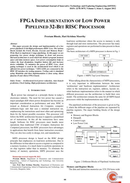
International Journal <strong>of</strong> Innovative Technology and Exploring Engineering (IJITEE)ISSN: 2278-3075, Volume-1, Issue-3, August 2012<strong>FPGA</strong> IMPLEMENTATION OF LOW POWERPIPELINED <strong>32</strong>-BIT RISC PROCESSORPreetam Bhosle, Hari Krishna MoorthyAbstractThis paper presents the design and implementation <strong>of</strong> a lowpower pipelined <strong>32</strong>-bit High performance RISC Core. The variousblocks include the Fetch, Decode, Execute and Memory Read /Write Back to implement 4 stage pipelining. In this paper we areproposing low power design technique in front end process.Harvard architecture is used which has distinct program memoryspace and data memory space. <strong>Low</strong> power consumption helps toreduce the heat dissipation, lengthen battery life and increasedevice reliability. To minimize the power <strong>of</strong> RISC Core, clockgating technique is used in the architectural level which is anefficient low power technique. 7-SEG LEDs are connected to theRISC IO interface for testing purpose, Verilog code is simulatedusing Modelsim and then implementation is done using AlteraQuartus II and Altera <strong>FPGA</strong> board.Index Terms – Architectural level power reduction, Auto branchprediction, Clock Gating, High performance architecture.I. INTRODUCTION<strong>Low</strong> power has emerged as a principle theme in today‟selectronics industry. The need for low power has caused amajor paradigm shift where power dissipation has become animportant consideration as performance and area. RISC istermed as Reduced Instruction Set Computer, computerarithmetic-logic unit that uses a minimal instruction set,emphasizing the instructions used most <strong>of</strong>ten and optimizingthem for the fastest possible execution. This processor willfollow the RISC architecture because it supports a predefinedset <strong>of</strong> instructions. In this all the instructions have samelength. S<strong>of</strong>tware for RISC processors must handle moreoperations than traditional CISC [Complex Instruction SetComputer] processors, but RISC processors have advantagesin applications that benefit from faster instruction execution.They are also less costly to design, test, and manufacture.load/store architecture where the access to memory is onlythrough load and store instructions. The processor has manyregisters and operations are performed in data present in thoseregisters.The basic architecture <strong>of</strong> a MIPS processor is shown in Fig. 1Figure: 1 MIPS Top Level StructureWhen talking about the characteristics <strong>of</strong> MIPS processors,it is very important to differentiate between the terms„architecture‟ and „hardware implementation‟. Architecturerefers to the instruction set, registers, address, layouts etc.while hardware implementation refers to the manner in whichdifferent processors use the architecture to build their ownmodel. The architecture remains the same for all MIPS basedprocessors while the implementations may differ.The pipelined architecture <strong>of</strong> the processor is given in Fig.2, where the different stages <strong>of</strong> the pipeline are separated bypipeline registers. The major building blocks <strong>of</strong> the designinclude Memory and Register Blocks Datapath Control Logic <strong>Low</strong> <strong>Power</strong> Unit.MIPS processor design is based on the RISC designprinciple that emphasizes on load/store architecture. Due tothe difference in time taken to access a register as compared toa memory location, it is much faster to perform operations inon chip registers rather than in memory. To eliminate thelatency <strong>of</strong> memory operations, MIPS processor uses theManuscript received August 08, 2012.Preetam Bhosle, Department <strong>of</strong> Electronics and CommunicationEngineering, , School <strong>of</strong> Engineering and Technology, Jain UniversityBangalore, India.Asst. Pr<strong>of</strong>. Hari Krishna Moorthy, Department <strong>of</strong> Electronics andCommunication Engineering, School <strong>of</strong> Engineering and Technology, JainUniversity, Bangalore, India.Figure: 2 Different Blocks <strong>of</strong> <strong>Pipelined</strong> ArchitectureMemory and Register BlocksThe data and instruction memories are <strong>32</strong>X 256 bytes wide66
<strong>FPGA</strong> IMPLEMENTATION OF LOW POWER PIPELINED <strong>32</strong>-BIT RISC PROCESSORand <strong>32</strong>X1024 bytes wide respectively while the register blockis <strong>of</strong> size <strong>32</strong> bytes. The instruction memory is implemented asa single port on-chip distributed ROM while the data memoryis implemented as a single port on-chip block RAM inside the<strong>FPGA</strong>.DatapathThe pipeline stages for different type <strong>of</strong> instructions areprocessed as follows, in the fetch stage, instructions arefetched at every cycle from the instruction memory whoseaddress is pointed by the program counter (PC). During thedecode stage, the registers are read from the register file andthe opcode is passed to the control unit which asserts therequired control signals. Sign extension is also done for thecalculation <strong>of</strong> effective address. In the execute stage, forRegister type instructions, the ALU operations are performedaccording to the ALU operation control signals and for loadand store instructions, effective address calculation is done.The load and store instructions write to and read from the datamemory in the memory stage while the ALU results and thedata read from the data memory are written in to the registerfile by the register type and load instructions respectively inthe write-back stage.Control LogicThe pipeline is controlled by setting control values duringeach pipeline stage. Each control signal is active only during asingle pipeline stage and hence the control lines can bedivided according to the four pipelined stages. These signalswill be forwarded to the adjacent stage through the pipelineregisters.Data forwarding cannot prevent all pipeline stalls. When adata requested by a load instruction has not yet becomeavailable it leads to load-use hazards. To resolve this hazard,the pipeline is stalled by the unit for one stage and thencontinues with the forwarding <strong>of</strong> data.<strong>Low</strong> <strong>Power</strong> UnitThe main power reducing technique that has been exploredin this architecture is clock gating. Clock gating is a methodwhere the clock signal is prevented from reaching the variousmodules <strong>of</strong> the processor. The absence <strong>of</strong> the clock signalprevents any register and/or flip-flop from changing theirvalue. As a result <strong>of</strong> this, the input to any combinational logiccircuit remains unchanged, and thus no switching activitytakes place in those circuits. Since, in CMOS circuits, most <strong>of</strong>the power dissipation results from switching activity, clockgating greatly reduces the overall power consumption.II. PROPOSED SYSTEMThe RISC processor was designed using pipelinedarchitecture; through this the speed <strong>of</strong> the operation as well asoverall performance was increased. In this 4-stage pipeliningis implemented.The 4 stages <strong>of</strong> pipeline are1. Fetch2. Decode3. Execute4. Memory Read / Write Back.During the design process, low power technique wasincluded in the architectural level, also this methods isexpected to be efficient than back-end low power reductiontechniques. For increasing the performance, latch based clockgating technique is used. Clock gating is the most popularmethod for power reduction <strong>of</strong> clock signals. When the clocksignal <strong>of</strong> a functional module is not required for someextended period, we using a gating function to turn <strong>of</strong>f theclock feeding the module. Clock gating saves power byreducing unnecessary clock activities inside the gatedmodule. The design complexity and performance degradation<strong>of</strong> clock gating are generally manageable.<strong>Processor</strong>s with pipelining consist internally <strong>of</strong> stages(modules) which can semi-independently work on separatemicroinstructions. Each stage is linked by flip flops to the nextstage (like a "chain") so that the stage's output is an input toanother stage until the job <strong>of</strong> processing instructions is done.Such organization <strong>of</strong> processor internal modules reduces theinstruction's overall processing time. An instruction pipelineis said to be fully pipelined if it can accept a new instructionevery clock cycle. A pipeline that is not fully pipelined haswait cycles that delay the progress <strong>of</strong> the pipeline.The proposed architecture is general-purpose RISCprocessor with pipelining feature; it gets instructions on aregular basis using dedicated buses to its memory, executesall its native instructions in stages with pipelining. It cancommunicate with external devices with its dedicated parallelIO interface.There are basically three types <strong>of</strong> instructions namelyArithmetic and Logical Instructions (ALU instructions),Load/Store instructions and Branch instructions.1. ALU Instructions:Arithmetic operations either take two registers as operandsor take one register and a sign extended immediate value as anoperand. Some arithmetic instructions are ADD, SUB, andMUL. The result is stored in a third register. Logicaloperations such as AND OR, XOR do not usuallydifferentiate between <strong>32</strong>-bit and 64-bit. Other logicalinstructions are NAND, NOR, NOT etc.2. Load/Store Instructions:Usually take a register (base register) as an operand and a16-bit immediate value. The sum <strong>of</strong> the two will create theeffective address. A second register acts as a source in thecase <strong>of</strong> a load operation. In the case <strong>of</strong> a store operation thesecond register contains the data to be stored. Examples are:LW, SW etc.3. Branches and Jumps Conditional branches are transfer<strong>of</strong> control. A branch causes an immediate value to be added tothe current program counter. Some common branchinstructions are BZ (Branch Zero), BRZ (Branch RegisterZero), JMP (Jump Instruction), JMPZ (Jump when zero) etc.III. ARCHITECTUREThe proposed architecture consists <strong>of</strong> 4-stagesnamely:67
International Journal <strong>of</strong> Innovative Technology and Exploring Engineering (IJITEE)ISSN: 2278-3075, Volume-1, Issue-3, August 2012 Instruction Fetch (IF), Instruction Decode (ID), Execution unit (EX), Memory Unit (MU), Memory write/read unit <strong>Low</strong> power unit along with 4 general purposeregisters namely Register0, Register1, Register2 andRegister3.Table 1: Instruction set for the proposed ArchitectureFig. 3 Proposed Architecture <strong>of</strong> <strong>Low</strong> power RISC<strong>Processor</strong>.Instruction Fetch (IF):The Instruction Fetch stage is where a program counter (8bit) will pull the next instruction from the correct location inprogram memory. In addition the program counter will beupdated with either the next instruction location sequentially,or the instruction location as determined by a branch.Instruction Decode (ID):The Instruction Decode stage is where the control unitdetermines what values the control lines must be set todepending on the instruction. In addition, hazard detection isimplemented in this stage, and all necessary values are fetchedfrom the register banks.Execute Unit (EX):The Execute stage is where the instruction is actually sentto the ALU and executed. If necessary, branch locations arecalculated in this stage as well. Additionally, this is the stagewhere the forwarding unit will determine whether the output<strong>of</strong> the ALU or the memory unit should be forwarded to theALU‟s inputs.Memory Unit (MU):Finally, the Memory Access stage is where, if necessary,system memory is accessed for data. Also, if a write to datamemory is required by the instruction it is done in this stage.In order to avoid additional complications it is assumed that asingle read or write is accomplished within a single CPUclock cycle.InstructionInstruction WordOpcode Source DestinationActionNOP 0000 ?? ?? NoneADD 0001 Src DstDst
<strong>FPGA</strong> IMPLEMENTATION OF LOW POWER PIPELINED <strong>32</strong>-BIT RISC PROCESSORADD: Dst = Src + DstOperands var1 and var2 stored in register locations Src andDst are added and written to the destination register specifiedby Alu_out.SUB: Dst = Src - DstOperand var2 is subtracted from Operand var1 and is writtento Alu_out.MUL: Dst
International Journal <strong>of</strong> Innovative Technology and Exploring Engineering (IJITEE)ISSN: 2278-3075, Volume-1, Issue-3, August 2012Figure: 7 Analysis and Synthesis SummaryFigure: 5 Simulation WaveformFigure: 8 <strong>Power</strong> Analysis SummaryFigure: 6 Flow SummaryV. CONCLUSIONThe design <strong>of</strong> 4-stage <strong>32</strong>-bit low power RISC processorperforming arithmetic, logical, memory and branchinstructions is presented in this paper. An architecture isdevised in order to felicitate the writing <strong>of</strong> codes inVerilog. The Verilog coding synthesis issues play a vitalrole in the speed-area optimality because RTL schematicdepends heavily on how we have coded in Verilog. Thedesign is simulated on ModelSim SE 6.4e tool and thensynthesized and verified on Altera <strong>FPGA</strong> board. Theproposed architecture is able to prevent pipelining fromflushing when branch instruction occurs and able to providehalt support. It can be inferred from the synthesis report thatproposed architecture <strong>of</strong>fers speed which is approximately110.92 MHz‟s.ACKNOWLEDGMENTThis paper is dedicated to our parents, and family for theirlove, endless support and encouragement. We would alsothank our friends, Mr. B. Ahmed and Mr. Sunil for theirconstant support and guidance.We would like to thank the Department <strong>of</strong> Electronics andCommunication Engineering, management <strong>of</strong> School <strong>of</strong>70
<strong>FPGA</strong> IMPLEMENTATION OF LOW POWER PIPELINED <strong>32</strong>-BIT RISC PROCESSOREngineering and Technology, Jain University, Bangalore fortheir constant support and encouragement in undertaking thework.REFERENCES[1] M.E. Hopkins, "A Perspective on the 801/Reduced Instruction SetComputer", IBM Systems Journal, Vol. 26, No. 1, pp. 107-121, 1987.[2] John L. Hennessy, David A. Patterson, Computer Architecture AQuantitative Approach, Morgan Kaufmann Publishers, San Mateo, 1990.[3] R.R. Oehler and R.D. Groves, "IBM RISC System/6000 processorarchitecture", IBM Journal <strong>of</strong> Research and Development, Vol. 34, No. 1,pp. 23-36, 1990.[4] Michael J. Flynn, Chad L. Mitchell and Johannes M. Mulder, "And Nowa Case for More Complex Instruction Sets", IEEE Journal on Computer, pp.71-83, 1987.Preetam Bhosle obtained Bachelor <strong>of</strong> Engineering in Electronics andCommunication Engineering from Appa Institute<strong>of</strong> Engineering and Technology, Gulbarga, VTU,Belgaum in 2010 and now pursuing Master <strong>of</strong>Technology (SP&VLSI) in Electronics andCommunication Engineering, from School <strong>of</strong>Engineering and Technology, Jain University,Bangalore-Karnataka, India.Hari Krishna Moorthy obtained Bachelor <strong>of</strong> Engineering from G.V.I.T.K.G.F, Bangalore University in 2001 and Master<strong>of</strong> Engineering from Sathyabama University,Chennai in the year 2007. Assistant Pr<strong>of</strong>essor inthe Department <strong>of</strong> Electronics andCommunication Engineering, School <strong>of</strong>Engineering and Technology,Jain University,Bangalore-Karnataka, India.[5] Norman P. Jouppi, David W. Wall, "Available Instruction-LevelParallelism for Superscalar and Superpipelined Machines", IEEEProceedings <strong>of</strong> the Third International Conference on ArchitecturalSupport for Programming Languages and Operating Systems, Boston,Mass, pp. 272-282, 1989.[6] Michael Butler, Tse-Yu Yeh, Yale Patt, Mitch Alsup, Hunter Scales,Michael Shebanow, "Single Instruction Stream Parallelism is Greater thanTwo", ACM Proceedings <strong>of</strong> the 18th Annual International Symposium onComputer Architecture, pp. 276-286, 1991.[7] Michael D. Smith, Mike Johnson and Mark A. Horowitz, "Limits onMultiple Instruction Issue", IEEE Proceedings <strong>of</strong> the Third InternationalConference on Architectural Support for Programming Languages andOperating Systems, Boston, Mass., pp. 290-302, 1989.[8] Kui Yi, Yue-Hua Ding, “<strong>32</strong>-bit RISC CPU based on MIPS” ,Proceedings <strong>of</strong> Second Pacific-Asia Conference on web mining andweb-based application, pp. 124 - 128, 2009.[9] Bassoy, C.S.,Manteuffel, H., Mayer-Lindenberg, F.,“SHARF: An<strong>FPGA</strong>-Based customizable processor architecture”, Proceedings <strong>of</strong>International Conference on Field Programmable Logic and applications,pp.516-520, 2009.[10] Gautham,P., Parthasarathy, R., Balasubramanian, K., “<strong>Low</strong>-<strong>Power</strong><strong>Pipelined</strong> MIPS <strong>Processor</strong> Design”, Proceedings <strong>of</strong> the 12th InternationalSymposium on Integrated Circuits, ISIC, pp. 462 – 465, 2010.[11] Adamec, F.,Fryza, T., “Design and Optimization <strong>of</strong> ColdFire CPUArithmetic and Logic Unit”, Proceedings <strong>of</strong> 16 th International Conferenceon mixed design <strong>of</strong> integrated circuits & Systems, pp. 699 – 702, 2009.[12] Sh<strong>of</strong>iqul Islam, Debanjan Chattopadhyay, Manoja Kumar Das, VNeelima; Rahul Sarkar, “Design <strong>of</strong> High Speed <strong>Pipelined</strong> Execution Unit<strong>of</strong> <strong>32</strong>-bit RISC <strong>Processor</strong>” India Conference, Annual IEEE , pp. 1 - 5, 2006.[13] Geun-young Jeong; Ju-sung Park; Science and Technology, “ Design <strong>of</strong><strong>32</strong>-bit RISC <strong>Processor</strong> and efficient verification” 2003, Proceeding <strong>of</strong> the7th Korea-Russia International Symposium, vol.2, pp. 222 - 227 , 2003.[14] J. Hennessy and D. Patterson, Computer Architecture: A QuantitativeApproach, Morgan & Kaufman Publishers, San Mateo, California.[15] G.M.Amdahl, G.A. Blaauw, F.P. Brooks, "Architecture <strong>of</strong> the IBMSystem/360, IBM Journal <strong>of</strong> Research and Development, vol.8,pp.87-101, April 1964.71